di cvd diamond dia mo neutron detectors nd d arnaldo galbiati · neutron detectors 30 october 2009...
TRANSCRIPT

Diam
ond Detectors Ltd
Diam
ond Detectors Ltd
Diam
ond Detectors Ltd
CVD Diamond CVD Diamond Neutron DetectorsNeutron Detectors
30 October 2009 1Arnaldo Galbiati
Arnaldo Galbiati

Diam
ond Detectors Ltd
Diam
ond Detectors Ltd
Diam
ond Detectors Ltd
Diamond Neutron DetectorsDiamond Neutron Detectors
Properties of Diamond
Diamond Detectors
CVD Diamond Neutron Detectors
Introduction to DDL
30 October 2009 2Arnaldo Galbiati

Diam
ond Detectors Ltd
Diam
ond Detectors Ltd
1920 Diamond demonstrates UV response1940 Diamond used to detect ionising nuclear radiation1950 – 60 Interactions of Alpha and high energy fast electrons with diamond studied1962 Photoconductivity of Natural Diamond investigated1970 Advances made in forming electrical contacts to diamond1980 Commercial x-ray dosimeters for medical applications
Early 90’s Advances made in quality of polycrystalline CVD diamond (pCVD) pCVD recommended for use in Super Conducting Super Collider Employed as commercial solar blind UV detector. Late 90’s Beam position monitors for synchrotrons Charge Collection distance > 200 µm Many high energy physics detector applications.
2000 DeBeers Industrial Diamond patents manufacturing procedure for High purity single crystal diamond with superior electronic characteristics 2002 DeBeers Industrial Diamond forms Element Six 2006 E6 perfects volume manufacturing process for electronic grade” materials 2007 DDL formed by Element Six2008 DDL patents metallisation development DDL achieves surface polishing improvements <1nm roughness DDL 50% acquired by BAE Systems
Diamond Detectors Limited 3
Diamond as a detector is not a new technology and as early as 1920's highly selected natural diamonds were being used for UV detectors. The recent commercial availability of high purity single crystal diamond with excellent bulk uniformity is however a new development.

Diam
ond Detectors Ltd
Diam
ond Detectors Ltd
Diam
ond Detectors Ltd
Diamond Detectors
30 October 2009 4Diamond Detectors Limited
Properties of Diamond

Diam
ond Detectors Ltd
Diam
ond Detectors Ltd
Arnaldo Galbiati
Properties of Diamond
Diamond radiation detectors are able to detect deep UV photons, X-rays, gamma rays, electrons, alpha particles, charged ions and neutrons, with a dynamic range in energies spanning from 5.5 eV up to GeV of cosmic rays.
Since the bandgap of diamond is 5.5 eV this leads into a negligible dark current noise at room temperature with no need for cooling.

Diam
ond Detectors Ltd
Diam
ond Detectors Ltd
Diamond tetrahedronDiamond tetrahedron
(from www.pdymorf.net/matter14.htm)

Diam
ond Detectors Ltd
Diam
ond Detectors Ltd
F.P. Bundy, The P,T Phase and Reaction diagram for elemental Carbon, 1979; J. Geophys. Res. 85 (B12) (1980) p. 6930
Phase Diagram for Carbon

Diam
ond Detectors Ltd
Diam
ond Detectors Ltd
Why use Diamond?Why use Diamond?Radiation hardness -> no frequent replacementsHigh mobility of free charges-> Fast responseCompact volume solid state detectorRoom temperature operation-> No CoolingResistivity ~5 orders of magnitude > SiliconLow leakage current -> No need for pn junction

Diam
ond Detectors Ltd
Diam
ond Detectors Ltd
30 October 2009 Diamond Detectors Limited 9
Properties of Diamond
Intrinsic Material PropertiesIntrinsic Material Properties

Diam
ond Detectors Ltd
Diam
ond Detectors Ltd
Why use Diamond?Why use Diamond?The special characteristics of diamond allow its use in
extreme environmental conditions like high temperature, high radiation, and highly corrosive environments.
Hence, its use for example in:
High energy physics as Beam Condition Monitor and particle tracker at CERN, As a radiotherapy dosimeter In X-ray synchrotron radiation monitoring (e.g., ESRF,
Grenoble, France) as UV and neutron detector at the Joint European
Torus, Culham, U.K.

Diam
ond Detectors Ltd
Diam
ond Detectors Ltd
First Radiation Detectors (1945)First Radiation Detectors (1945)From Natural DiamondFrom Natural Diamond
At that time counting properties were found to be uncontrollable, depending upon the crystal and the type of radiation. Furthermore, charge polarization occurred, leading to a progressive reduction in both counting rate and pulse amplitude as a function of the time of irradiation.P.J. VAN HEERDEN, Thesis Utrecht, 1945.R. HOFSTADTER., Phys. Rev. 73 (1948) 631.Since 1970, the attractive properties of diamond for radiation detection were demonstrated by KOZLOV et al. from mono-crystalline diamond stones of extremely high electronic quality.

Diam
ond Detectors Ltd
Diam
ond Detectors Ltd
Alpha Particle Detection Alpha Particle Detection History in DiamondHistory in Diamond
Bergonzo et al., Diamond and Related Materials, Volume 10, Issues 3-7, March-July (2001), 631-638
Kaneko et al. 2003

Diam
ond Detectors Ltd
Diam
ond Detectors Ltd
sc CVD Diamond Detectorssc CVD Diamond DetectorsHigh Purity Single Crystal CVD Diamond:100 % charge collection efficiency 100 % counting detection efficiency
0.4-1 % energy resolution (Alpha 5 MeV)
Reference Figure from: J.H. Kaneko et al. / Nuclear Instruments and Methods in Physics Research A 505 (2003) 187–190
J.H. Kaneko et al. 2003l

Diam
ond Detectors Ltd
Diam
ond Detectors Ltd
sc CVD Diamond Detectorssc CVD Diamond DetectorsCommercially Available High Purity Single Crystal CVD Diamond:100 % charge collection efficiency 100 % counting detection efficiency 0.4-1 % energy resolution (Alpha 5 MeV)No pumping (priming) effects Long term stability

Diam
ond Detectors Ltd
Diam
ond Detectors Ltd
Diamond radiation detectors are generally designed as a parallelepiped solid-state ionization chamber. A charged particle, or a photon with energy above the bandgap,
passes through the diamond and ionizes it (energy to form e-h pair: 13 eV) generating electron–hole pairs, which are separated by the electric field between the electrodes.
•Fast neutrons are detected directly in the bulk of the intrinsic diamond layer through the 12C (n,α) 9Be and 12C (n,n')12C* reactions*. The produced 9Be and α ions have a total energy:
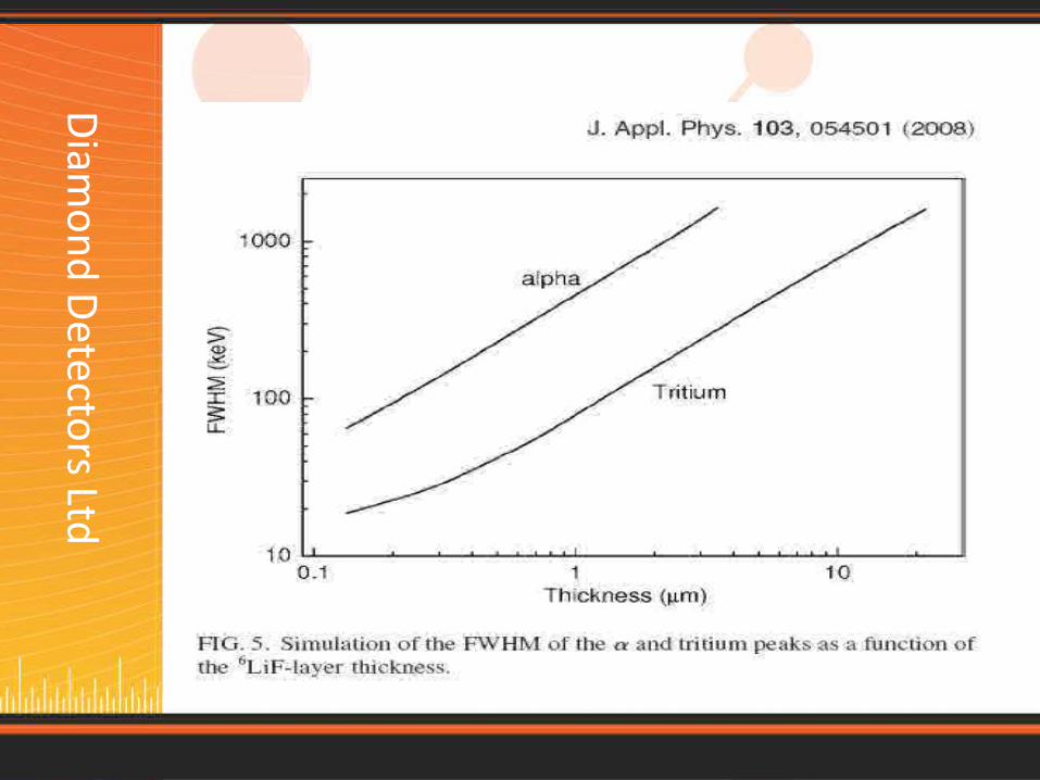
Eα + Βe = Εn – 5.7 MeV where Εn is the energy of the impinging neutron. •To detect both fast and thermal neutrons a layer of 6LiF or 10B allows the conversion of low energy neutrons into highly ionizing particles.
*M. Pillon, M. Angelone, A.V. Krasilnikov, Nucl. Instr. and Meth. Phys. Res. B 101 (1995) 473.
Radiation Detection in Diamond

Diam
ond Detectors Ltd
Diam
ond Detectors Ltd
•Diamond has the highest atomic density of any material
•This translates into a high neutron efficiency per unit volume.
•“Diamond appears to have the highest intrinsic efficiency for fission neutron detection per unit thickness, and hence per unit volume”*.
* G .J. S chm i d et al . / N u c l ear I n st r u m en t s an d M eth o d s i n P h y si c s R esear c h A 527 (2004) 554–561
Diamond intrinsic high efficiency for fission neutron detection

Diam
ond Detectors Ltd
Diam
ond Detectors Ltd
G .J. S chm i d et al . / N u c l ear I n st r u m en t s an d M eth o d s i n P h y si c s R esear c h A 527 (2004) 554–561
Diamond intrinsic high efficiency for fission neutron detection

Diam
ond Detectors Ltd
Diam
ond Detectors Ltd
“Based on the diamond neutron data, along with the total neutron yields as acquired via associated particle counting, it is possible to extract experimental values for the intrinsic efficiency per unit thickness, and to compare this to calculation. For our diamond sensor, with an energy threshold of ~20– 30 keV (estimated carbon recoil energy), the experimental efficiency values at 2.5 and 14 MeV are 2.2 and 2.4%/mm respectively”*
*G .J. S c hm i d et al . / N u c l ear I n st r u m en t s an d M eth o d s i n P h y si c s R esear c h A 527 (2004) 554–561
Diamond experimental efficiency for fission neutron detection
At 14.1 and 14.9 MeV, the spectrum shape is due to a combination of elastic scattering, inelastic scattering, and (n ,a) reactions, as discussed theoretically by Pillon [M. Pillon, M. Angelone, A.V. Krasilnikov, Nucl. Instr. and Meth. Phys. Res. B 101 (1995) 473.]

Diam
ond Detectors Ltd
Diam
ond Detectors Ltd
Bergonzo et al.

Diam
ond Detectors Ltd
Diam
ond Detectors Ltd
http://www-norhdia.gsi.de/talks/4th/G_Verona-Rinati.pdfSingle crystal CVD diamond neutron detectors in a p-type/intrinsic/metal layered structure - Gianluca Verona-Rinati, Uni Roma Tor Vergata

Diam
ond Detectors Ltd
Diam
ond Detectors Ltd
http://www-norhdia.gsi.de/talks/4th/G_Verona-Rinati.pdf

Diam
ond Detectors Ltd
Diam
ond Detectors Ltd

Diam
ond Detectors Ltd
Diam
ond Detectors Ltd

Diam
ond Detectors Ltd
Diam
ond Detectors Ltd
Diamond DetectorDiamond Detector14 MeV Neutron Spectroscopy14 MeV Neutron Spectroscopy

Diam
ond Detectors Ltd
Diam
ond Detectors Ltd
Almaviva et al. J. Appl. Phys. 103, 054501 2008 http://www-norhdia.gsi.de/talks/4th/G_Verona-Rinati.pdf
6LiF Layer Thickness

Diam
ond Detectors Ltd
Diam
ond Detectors Ltd
http://www-norhdia.gsi.de/talks/4th/G_Verona-Rinati.pdf

Diam
ond Detectors Ltd
Diam
ond Detectors Ltd

Diam
ond Detectors Ltd
Diam
ond Detectors Ltd
Diamond Neutron Detectors Counting Sensitivity under thermal irradiation
Almaviva et al. J. Appl. Phys. 103, 054501 2008
Diam
ond Detectors Ltd
Diam
ond Detectors Ltd

Diam
ond Detectors Ltd
Diam
ond Detectors Ltd
Diamond DetectorDiamond Detector14 MeV Neutron Spectroscopy14 MeV Neutron Spectroscopy
Almaviva et al. J. Appl. Phys. 103, 054501 2008

Diam
ond Detectors Ltd
Diam
ond Detectors Ltd
14 MeV Neutron pulse14 MeV Neutron pulsesc CVD Diamond Detector+DBA (2GHz amplifier)sc CVD Diamond Detector+DBA (2GHz amplifier)
ANGELONE et al.: “NEUTRON DETECTORS BASED UPON ARTIFICIAL SINGLE CRYSTAL DIAMOND IEEE TRANSACTIONS ON NUCLEAR SCIENCE”, VOL. 56, NO. 4, AUGUST 2009

Diam
ond Detectors Ltd
Diam
ond Detectors Ltd
DBA-IV (2GHz Broadband Amplifier)DBA-IV (2GHz Broadband Amplifier)
•The DBA-IV 2GHz Broadband amplifier is available through www.diamonddetectors.com

Diam
ond Detectors Ltd
Diam
ond Detectors Ltd
http://www-norhdia.gsi.de/talks/4th/G_Verona-Rinati.pdf

Diam
ond Detectors Ltd
Diam
ond Detectors Ltd
http://www-norhdia.gsi.de/talks/4th/G_Verona-Rinati.pdf

Diam
ond Detectors Ltd
Diam
ond Detectors Ltd
http://www-norhdia.gsi.de/talks/4th/G_Verona-Rinati.pdf

Diam
ond Detectors Ltd
Diam
ond Detectors Ltd
http://www-norhdia.gsi.de/talks/4th/G_Verona-Rinati.pdf

Diam
ond Detectors Ltd
Diam
ond Detectors Ltd
http://www-norhdia.gsi.de/talks/4th/G_Verona-Rinati.pdf
Diamond Neutron Detectors Tested at Frascati Neutron Generator and JET

Diam
ond Detectors Ltd
Diam
ond Detectors Ltd
Neutron Diamond DetectorsNeutron Diamond Detectorsnew ENEA-DDL collaborationnew ENEA-DDL collaboration
“The benefits to industry in Europe of working with JET are more than simply the value of the contracts received. The technologies developed can have applications also in other fields. A recent example is a detector made of artificial diamond developed by the Italian Association ENEA for measuring the number and energy spectrum of neutrons emitted from the JET plasma.” Lorne Horton, JET Insight June 2009.

Diam
ond Detectors Ltd
Diam
ond Detectors Ltd
Diam
ond Detectors Ltd
Diamond Detectors
30 October 2009 39Diamond Detectors Limited
CVD Diamond HistoryProperties of DiamondIntroduction to DDLDDL Proprietary Contact Technology

Diam
ond Detectors Ltd
Diam
ond Detectors Ltd
30 October 2009 Diamond Detectors Limited 40
JJune 2007, DDL Moves into new office, Poole, Dorset
22008, BAE systems acquires 50% share in DDL
PPress release Thursday 3rd May 2007
“Element Six Spins Out New Company to Develop Diamond Detectors…….
Introduction to DDL
Diam
ond Detectors Ltd
Diam
ond Detectors Ltd
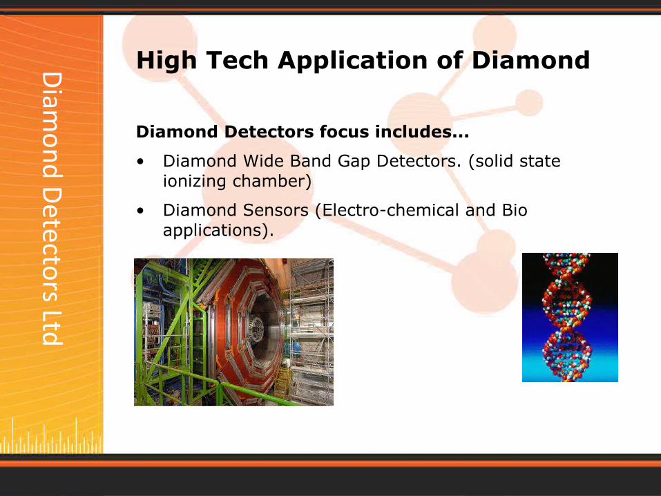
High Tech Application of Diamond
Diamond Detectors focus includes...
• Diamond Wide Band Gap Detectors. (solid state ionizing chamber)
i
• Diamond Sensors (Electro-chemical and Bio applications).

Diam
ond Detectors Ltd
Diam
ond Detectors Ltd
Introduction to DDL
30 October 2009 Diamond Detectors Limited 42
FacilitiesDiamond Lab
Laser LabChemistry Lab
Lithography and Assembly Clean rooms. (class 1000 & 10000)
Design Suite
ExpertiseMaterial Processing
Lapping & Polishing ProcessesLaser Dicing & Shaping
Metallization (e.g. Ti, Pt, Au, Al..)Neutron Scintillation Coating 6LiF
Lithography (sandwich,strips,pixels)Die Fabrication and Test
Die/Wire Bonding.Packaging
Characterisation.Electronics Development
“From Concept through Design & Prototype to Manufacture”

Diam
ond Detectors Ltd
Diam
ond Detectors Ltd
Introduction to DDL
30 October 2009 Diamond Detectors Limited 43
Manufactured DevicesConcept - Design
“From Concept through Design & Prototype to Manufacture”

Diam
ond Detectors Ltd
Diam
ond Detectors Ltd
Introduction to DDL
30 October 2009 Diamond Detectors Limited 44
“From Concept through Design & Prototype to Manufacture”
Laser cutting, dicing & sputtering system
Quazer Laser D
icing
Magnetron Sputtering
Device Fabrication
Lapping, Polishing and Semi-automatic scaife
Optical Profiler N
T9100
Semi A
utomatic Scaife
MetallisationSputtering &
E-Beam
Evaporation & M
illing
Wire Bonding (Strip Detector)
Universal w
edge bonder (K&S
4523)
Dage 4000 W
ire bond pull tester
Alum
inium &
Gold w
edge and ball w
ire bonding
ball bonding (K&S 4124)

Diam
ond Detectors Ltd
Diam
ond Detectors Ltd
Introduction to DDL
30 October 2009 Diamond Detectors Limited 45
“From Concept through Design & Prototype to Manufacture”
Typical process specifications :-Polycrystalline standard polish Ra < 20nmPolycrystalline detector polish Ra < 12nm Polycrystalline Super polish Ra < 5nmSingle crystal detector polish Ra < 1nm Electronic / Device Characterisation
Characterisation
Diam
ond Detectors Ltd
Diam
ond Detectors Ltd
Diamond Detectors Limited
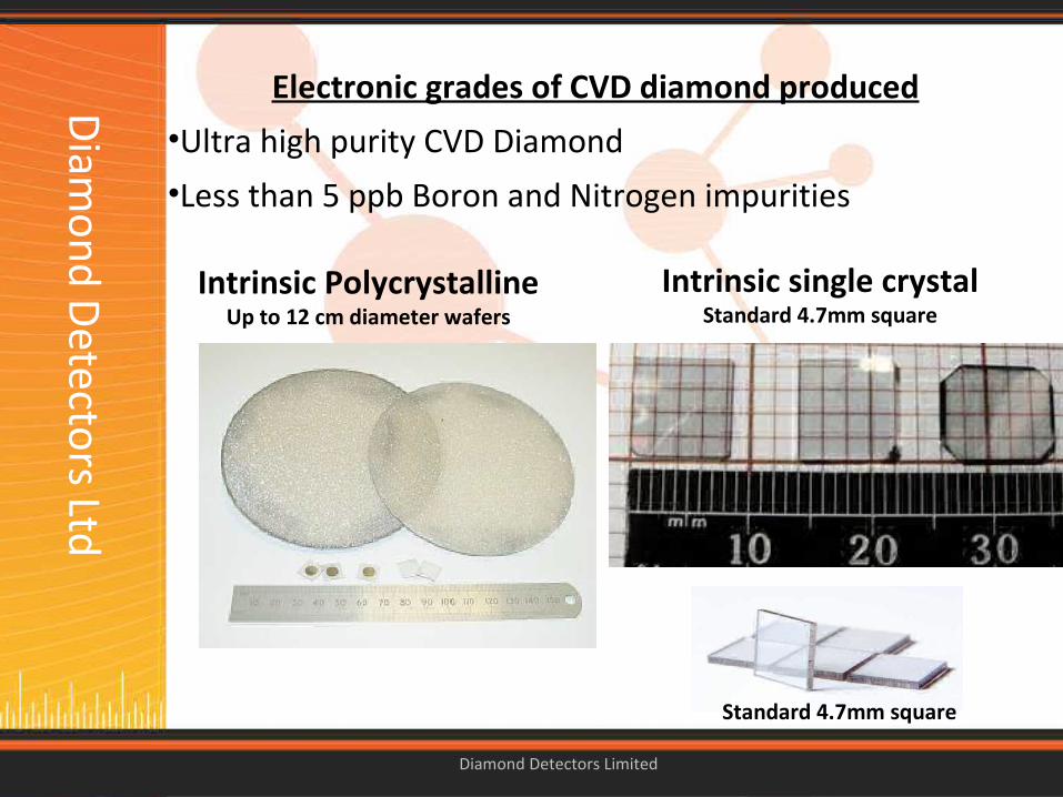
Electronic grades of CVD diamond produced
•Ultra high purity CVD Diamond
•Less than 5 ppb Boron and Nitrogen impurities
Intrinsic single crystalStandard 4.7mm square
Intrinsic PolycrystallineUp to 12 cm diameter wafers
Standard 4.7mm square

Diam
ond Detectors Ltd
Diam
ond Detectors Ltd
© 2008 Diamond Detectors Ltd
Example :- Diamond Radiation Detector Module as COB (Chip on Board) with electrical metal posts

Diam
ond Detectors Ltd
Diam
ond Detectors Ltd
© 2008 Diamond Detectors Ltd
Single Crystal Diamond Radiation Detector Standard Module [25mm Diameter] with SMA connector
© 2008 Diamond Detectors Ltd
(photo-realistic rendering by Solidworks softrware)
(

Diam
ond Detectors Ltd
Diam
ond Detectors Ltd
Diamond Radiation DetectorBeam Conditions Monitor
Quadrant Detector

Diam
ond Detectors Ltd
Diam
ond Detectors Ltd
© 2008 Diamond Detectors Ltd © 2008 Diamond Detectors Ltd
Example :- Diamond Radiation Detectors in BNC and TO-Metal Can

Diam
ond Detectors Ltd
Diam
ond Detectors Ltd
© 2008 Diamond Detectors Ltd
Example :- Diamond Radiation Detector (electrodes bonded from lateral sides not top and bottom)
Diamond Dimensions 5 x 1 x 0.5 mm
e.g.: directional information

Diam
ond Detectors Ltd
Diam
ond Detectors Ltd
© 2008 Diamond Detectors Ltd
Example :- Diamond Radiation Detector with robust electrical point contacts

Diam
ond Detectors Ltd
Diam
ond Detectors Ltd
© 2007 Diamond Detectors Ltd © 2007 Diamond Detectors Ltd
Example :- Diamond Radiation Detector Module with SMA and Chip in Board packaging

Diam
ond Detectors Ltd
Diam
ond Detectors Ltd
© 2008 Diamond Detectors Ltd
Single Crystal Diamond Radiation Detectors
(photo-realistic rendering by Solidworks softrware)
Standard Module [25mm Diameter] with SMA connector
Standard size: 4.7 x 4.7 x 0.5 mm
Can be laser cut and mechanically polished to create customized sizes and shapes, and or assembled in a mosaic or stack structure
Available standard thickness 50 μm to 500 μm
Minimum active volume size 1 x 1 x 0.5 mm
Standard electrical contact shapes (square and circle)
Customised electrical contact shapes
DDL proprietary contact
Customised electrical contact materials

Diam
ond Detectors Ltd
Diam
ond Detectors Ltd
Diam
ond Detectors Ltd
Diamond DetectorsCVD Diamond HistoryIntroduction to DDLProperties of DiamondDDL Proprietary Contact Technology
30 October 2009 55Diamond Detectors Limited

Diam
ond Detectors Ltd
Diam
ond Detectors Ltd
DDL Proprietary Contact Technology
Mechanical AdhesionSpecifically, the mechanical adhesion of the metal chosen as electrode on the diamond surface. A flatter smoother surface presents fewer adhesion points. When a metal is thermally evaporated on diamond it may not adhere and it could peel off after a short period of time with the consequent deterioration of the electrical signal measured and therefore a decrease in the lifetime of the device. Mechanical adhesion is a function of the diamond / contact interface.
Polarization EffectsPolarization phenomena occur when electric currents pass through diamond if the electrical contact is not able to extract and inject electrons fast enough. In this case, the neutrality of the crystal after the passage of ionizing nuclear radiations is not restored in the time interval between two consecutive events. As a result, charge accumulation occurs within the crystal and immobile carriers establish an electric field which acts in a direction opposite to the applied field produced by the external bias voltage V. The minimisation of polarization effects requires optimal injecting contacts.
Repeatable ResultsIf a device is to be commercially viable it should be consistent and stable in a variety of environmental conditions. Requires stable and resilient contacts.
Historically, there have been three main approaches to fabricate good electrical contacts on diamond:1. Damaging the diamond surface in order to disrupt the sp3 bonding.2. Using carbide forming metals like titanium or chromium to create a hybrid metal-diamond interface material .3. Doping of diamond during growth or using ion implantation.For example, to prepare good injecting contacts, several metals were used by Kozlov et al., for hole injection they used Ag, Au, Pt or C deposition, aluminium or boron implantation, for electron injection P, Li or C.
Diamond Detectors Limited (DDL) has patented an innovative metallization technique to maximize CVD diamond performance. Here we seek to highlight the issues and describe the solution.The development of CVD Diamond has made possible many new applications for detecting and sensing. However, manufacturing semiconductor devices in diamond present some interesting challenges due to diamond’s unique characteristics. Traditional or inadequate contact fabrication may result in poor mechanical adhesion, polarization effects and unrepeatable results.
Metallization (Electrical Contact Fabrication on CVD Diamond)
Galbiati et al. IEEE TNS VOL 56 N 4 AUGUST 2009 p1863

Diam
ond Detectors Ltd
Diam
ond Detectors Ltd
Galbiati et al. IEEE TNS VOL 56 N 4 AUGUST 2009 p1863
DDL Proprietary Contact Technology
Metallization (Electrical Contact Fabrication on CVD Diamond)

Diam
ond Detectors Ltd
Diam
ond Detectors Ltd
58
DDL Proprietary Contact Technology
DDLs solutionTo address the polarization issues mentioned above and to provide a method for forming an ohmic electrode that is also durable and stable for applications in diamond radiation detectors and diamond electronics, Diamond Detectors Ltd have developed and tested an innovative electrical contact using a very thin diamond like carbon layer. Diamond-like carbon (DLC) is a form of amorphous carbon between diamond and graphite, containing significant portion of sp3 bonded atoms in the matrix. DLC films can be grown when carbon is deposited under energetic (~10-100eV) bombardment, where the instantaneous local high temperature and pressure induce a proportion of carbon atoms to bond as diamond. The conditions for DLC deposition are obtained during a variety of methods, including CVD, laser ablation, magnetron sputtering, cathodic arc, and ion beam deposition.This innovative contact consists of a very thin (1-3 nm) diamond-like carbon film which is formed on a diamond substrate by means of Argon magnetron sputtering from a carbon target. The very thin DLC layer allows for the injection of both holes and electrons in the diamond substrate. Also, the DLC layer becomes a seed for the sputter deposition of high work function noble metals (Pt, Au) which allow metals to cohere to the diamond surface. As platinum and gold have a higher work function than diamond this permits electrons present at the diamond surface to be driven towards the noble metals via quantum mechanical tunnelling through the thin DLC layer acting as a quantum mechanical tunnelling junction.
DDL’s patented metallization technique provides a manufacturable, high adherence diamond / contact interface with minimal polarization effect while maximizing stability and contact resilience.
Metallization (Electrical Contact Fabrication on CVD Diamond)
Galbiati et al. IEEE TNS VOL 56 N 4 AUGUST 2009 p1863

Diam
ond Detectors Ltd
Diam
ond Detectors Ltd
59
DDL Proprietary Contact Technology
Dark Current Characteristics
Galbiati et al. IEEE TNS VOL 56 N 4 AUGUST 2009 p1863

Diam
ond Detectors Ltd
Diam
ond Detectors Ltd
Collaborating Opportunities ?
Custom design and prototype manufacture.
Let us help you develop a resilient detector/sensor technology for your application using our design tools, facilities and experience in collaboration with your R&D team.
Prototype to Product (cost engineering, batch processing and test)
Diamond Detectors Limited 60

Diam
ond Detectors Ltd
Diam
ond Detectors Ltd
Conclusion
High quality electronic CVD diamond radiation detectors are now readily available.
DDL has made significant investment to ensure we have the ability and tools to manufacture diamond prototypes leading to standard products for a range of applications including high energy physics, medical, civil nuclear and oil and gas.
DDL will continue to support the development of diamond applications with the aim to provide a range of standard products with datasheets.
30 October 2009 Diamond Detectors Limited 61

Diam
ond Detectors Ltd
Diam
ond Detectors Ltd
Diam
ond Detectors Ltd
Thank you
30 October 2009 62Diamond Detectors Limited

Diam
ond Detectors Ltd
Diam
ond Detectors Ltd
REFERENCES:
Bergonzo et al., Diamond and Related Materials, Volume 10, Issues 3-7, March-July (2001), 631-638
J.H. Kaneko et al. / Nuclear Instruments and Methods in Physics Research A 505 (2003) 187–190
Pomorski et al., Phys. Stat. Sol. (a) 202, No. 11 (2005)
Gianluca Verona-Rinati “Single crystal CVD diamond neutron detectors in a p-type/intrinsic/metal layered structure” , http://www-norhdia.gsi.de/talks/4th/G_Verona-Rinati.pdf
Galbiati et al. “Performance of Monocrystalline Diamond Radiation Detectors Fabricated Using TiW, Cr/Au and a Novel Ohmic DLC/Pt/Au Electrical Contact” IEEE TNS VOL 56 N 4 AUGUST 2009 p1863
Angelone et al.: “NEUTRON DETECTORS BASED UPON ARTIFICIAL SINGLE CRYSTAL DIAMOND” IEEE TRANSACTIONS ON NUCLEAR SCIENCE, VOL. 56, NO. 4, AUGUST 2009 pp.2275-2279
Almaviva et al.: “Thermal and fast neutron detection in chemical vapor depositionsingle-crystal diamond detectors” J. Appl. Phys. 103, 054501 2008
G.J. Schmid et al. “A neutron sensor based on single crystal CVD diamond”, Nuclear Instruments and Methods in Physics Research A 527 (2004) 554–561
M. Pillon, M. Angelone, A.V. Krasilnikov, Nucl. Instr. and Meth. Phys. Res. B 101 (1995) 473.