dhamodaran santhanagopalan, ph. d. - sop.uohyd.ac.insop.uohyd.ac.in/~appsp/dams/dhamodaran...
TRANSCRIPT

Curriculum Vitae
Dhamodaran Santhanagopalan, Ph. D.
Ramanujan Fellow & Assistant Professor Amrita Centre for Nanosciences and Molecular Medicine, Kochi.
Address Amrita Centre for Nanosciences and Molecular Medicine,
Amrita Institute of Medical Sciences,
Amrita Vishwa Vidyapeetham University, AIMS (P.O),
Ponekkara, Kochi – 682 041.
Kerala (INDIA).
Mobile: (+91) 8098489233 E-mail: [email protected] &
Web: https://www.amrita.edu/faculty/dhamodaran-santhanagopalan
Education:
2007: PhD in Physics, University of Hyderabad, India.
2001: Master of Philosophy in Physics, Pondicherry University, India. (First
Class, CGPA: 8.25/10).
2000: Master of Science in Physics, Pondicherry University, India. (First class,
CGPA: 7.24/10).
1998: Bachelor of Science in Physics, Periyar Arts College, Cuddalore
(Affiliated to University of Madras, Chennai).
Professional Appointments:
June, 2014 – Present: Amrita Centre for Nanosciences, Amrita Vishwa
Vidhyapeetham, Kochi.
April, 2011 – April, 2014: Postdoctoral Fellow in NanoEngineering, University of
California San Diego, USA. (Also Member of North Eastern Centre for Chemical
Energy Storage: funded by US Department of Energy, led by Stony Brook
University)
Jan, 2008 – March, 2011: Assistant Professor (Contract) in Physics, IIT Kanpur.
July, 2007 – Dec, 2007: Institute Postdoctoral Fellow in Physics, IIT Kanpur.
Research Visits:
Guest Researcher (2011 – 2014), Center for Functional Nanomaterials, Brookhaven
National Laboratory, New York.
Guest Researcher (2012: One year), Environmental and Molecular Science
Laboratory, Pacific Northwest National Laboratory, Washington.
Visiting Scientist (3rd
July 2006 – 21st July 2006), Accelerator Group, HMI, Berlin.
Recognitions, Committees and Memberships:
Editorial Board Member: International Journal of Nano Studies and Technology,
SciDoc Publishers, New York, USA. (http://www.scidoc.org/ijnst.php)
Core Committee Member, Ion beam complex, IIT Kanpur (2008-2010)
MRS Member (2012), IEEE Member (2009)

Curriculum Vitae: Dhamodaran
Areas of Research Interests:
Energy Storage and Conversion
Lithium ion batteries
Intercalation, Alloying and Conversion materials
Structure-property-performance
Nano-Photonics & Nano-fabrication
GaN Nanostructures and Devices
Surface Enhanced Raman Spectroscopy
Focused ion beams
Ion-solid interactions
Ion implantation
Ion beam analysis
Characterization techniques
Atom Probe tomography
Scanning probe microscopy
Electron Microscopy and Spectroscopy
Research Achievements and Experience:
Nano-fabrication using focused ion beams. First time fabrication of functional
solid-state nano-batteries and in-situ STEM/EELS electrochemical
investigations.
Laser assisted atom probe tomography of lithium ion battery materials
including LiFexMn1-xPO4 (0 < x < 1), LiMnO2 and FeF2 thin-films.
Single particle electrochemistry with LiFePO4 single crystals to understand
the influence of defects on the electrochemical cycling.
Pulsed Laser Deposition (PLD) fabrication of thin-film lithium ion batteries.
High vacuum systems and thin film based materials science (10 years).
Developed a thermal-CVD system for growth of III-nitride semiconductor
nanostructures.
Clean room protocols and working experience in both class 1000 and class
100.
Development of spectroscopic facilities including, photoluminescence and
cathodoluminescence at IIT Kanpur.
In-charge of complete installation of the 1.7MV Tandetron at IIT Kanpur,
India (2007 – 2008).
Designed, developed, installed and tested several ion beam facilities
including, ion-scattering and ion implantation systems (2007 – 2010).
Installed proton beam writing micro-beam facility at IIT Kanpur (Dec 2008 –
Dec 2009).
Research Guidance @ ACNS, Kochi (June 2014 – Present):
Binitha G, PhD student (On-going).
Anu Priya K H, PhD student (On-going).
Jude John, M.Tech Student (On-going).
Siva Reddy, M. Tech Student (On-going).
Sreejith PM, M.Tech Student (On-going)

Curriculum Vitae: Dhamodaran
Research Guidance @ UC San Diego:
Co-supervised a MS student, Thomas McGilvray, Degree Awarded 2012.
Co-supervised a PhD student, Ziying Wang, On-going.
Thesis (M.Tech) Supervision
Jitendra Katiyar – M.Tech., Aug 2010, Thesis: Novel synthesis of micro- and
nano-granular Fe-Cu alloys by EDM (Co-Guide: Prof. J. Ramkumar).
Research Students and Project Associates @ IIT Kanpur
G. Karthikeyan – PhD., (2008-2010), Electric discharge machining micro-
fabrication (Supervisor: Prof. J Ramkumar).
S. Kanmani Subbu – PhD., (2008-10), Spectroscopic and microscopic studies of
electric discharge micro-plasmas (Supervisor: Prof. J Ramkumar).
D. Sathish Chander – Project Assoc., (2009-10) CVD growth of III-N
nanostructures
Chandan Samantha – M.Sc., (2010-11) Synthesis and characterization of GaN
nanowires.
Amithabha Nandi – M.Sc., (2010-11) Hydrophobicity of randomly oriented GaN
nanowires.
Nilanjan Roy – M.Sc., (2010-11) Surface enhanced Raman scattering from FIB
patterned nanostructures of silver and gold.
Sanjai Singh – M.Sc-Phd (Dual: 2010-11) Fabrication of GaN Schottky diodes.
Arnab Dhabal – M.Sc (Integrated) (2010-11) Electrical studies of isolated GaN
nanowires.
Bhanu Prakash – M.Sc., (2009-10) Semi-continuous metallic templates: FIB
fabrication and surface enhanced Raman scattering.
T. F. S. L. Mawlong – M.Sc., (2008-09) Synthesis and characterization of InN
nanowires.
Teaching @ ACNS, Kochi (Aug 2014 – Present):
NT601: Introduction to Quantum Mechanics (Aug – Dec 2014, 15) (Core Course)
NT602: Physics of Semiconductor Devices (Aug – Dec 2015) (Core Course)
NT604: Electrical Energy Storage (Jan – May 2015) (Core Course)
NT605: Device Lab and Simulations (Jan – May 2015) (Lab Course)
NT607: Nanodevice Fabrication (Aug – Dec 2015) (Core Course)
NT714: Nanosensors (Aug – Dec 2014) (Elective Course)
NS606: Characterization of Nanomaterials (Jan – May 2016) (Core Course)
Teaching @ UC San Diego:
Guest lectured two modules as a part of Nano 111 course (2012, 2013 and 2014)
offered by Prof. Y. S. Meng at UC San Diego,
1. Optical Microscopy and Scanning Electron Microscopy
2. Focused Ion Beams for Nanofabrication.
Curriculum Vitae: Dhamodaran
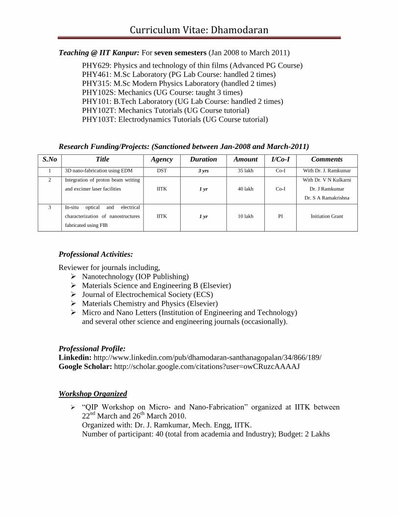
Teaching @ IIT Kanpur: For seven semesters (Jan 2008 to March 2011)
PHY629: Physics and technology of thin films (Advanced PG Course)
PHY461: M.Sc Laboratory (PG Lab Course: handled 2 times)
PHY315: M.Sc Modern Physics Laboratory (handled 2 times)
PHY102S: Mechanics (UG Course: taught 3 times)
PHY101: B.Tech Laboratory (UG Lab Course: handled 2 times)
PHY102T: Mechanics Tutorials (UG Course tutorial)
PHY103T: Electrodynamics Tutorials (UG Course tutorial)
Research Funding/Projects: (Sanctioned between Jan-2008 and March-2011)
S.No Title Agency Duration Amount I/Co-I Comments
1 3D nano-fabrication using EDM DST 3 yrs 35 lakh Co-I With Dr. J. Ramkumar
2 Integration of proton beam writing
and excimer laser facilities IITK 1 yr 40 lakh Co-I
With Dr. V N Kulkarni
Dr. J Ramkumar
Dr. S A Ramakrishna
3 In-situ optical and electrical
characterization of nanostructures
fabricated using FIB
IITK 1 yr 10 lakh PI Initiation Grant
Professional Activities:
Reviewer for journals including,
Nanotechnology (IOP Publishing)
Materials Science and Engineering B (Elsevier)
Journal of Electrochemical Society (ECS)
Materials Chemistry and Physics (Elsevier)
Micro and Nano Letters (Institution of Engineering and Technology)
and several other science and engineering journals (occasionally).
Professional Profile:
Linkedin: http://www.linkedin.com/pub/dhamodaran-santhanagopalan/34/866/189/
Google Scholar: http://scholar.google.com/citations?user=owCRuzcAAAAJ
Workshop Organized
“QIP Workshop on Micro- and Nano-Fabrication” organized at IITK between
22nd
March and 26th
March 2010.
Organized with: Dr. J. Ramkumar, Mech. Engg, IITK.
Number of participant: 40 (total from academia and Industry); Budget: 2 Lakhs

Curriculum Vitae: Dhamodaran
Journal Cover Page (*Corresponding Author)
S. Dhamodaran*
Nano Today Vol. 7, Issue 4 (2012)
The GaN nanostructure image was published on the cover page of the journal
D. Sathish Chander, J. Ramkumar and S. Dhamodaran*
CVD growth of GaN nanoflowers, “How does your nano-garden grow”
Materials Today 14, 231 (2011)
The GaN nanoflower image was published on the cover page of the journal
Manuscripts Communicated (*Corresponding Author)
I. Z. Wang, S. Dhamodaran, W. Zhang, F. Wang, H. Xin, K. He, J. Li, N. Dudney and
Y. S. Meng*
“In Situ STEM/EELS Observation of Cathode-Electrolyte Interfacial Phenomena in
All-Solid-State Batteries”
(Communicated).
Research Publications
50. S. Dhamodaran, D. K. Schreiber, D. E. Perea, S. Thevudasan, R. Martens, Y. Jassen,
P. G. Kalifah and Y. S. Meng*
“The Effect of Laser Power and Wavelength on the Measured Concentrations of
Lithium and Oxygen in LiFePO4 Using Laser Assisted Atom Probe Tomography”
Ultramicroscopy 148, 57 (2015).
49. S. Dhamodaran, D. Qian, T. Mcgilvray, Z. Wang, F. Wang, J. Graetz, N. Dudney,
Y. S. Meng*
“Interface limited lithium transport in all-solid-state nano-batteries”
J. Phys. Chem. Lett. 5, 298 (2014).
48. G. Sai Saravanan*, K. M. Bhata, S. Dhamodaran, A. P. Pathak, R. Muralidharan, H.
P. Vyas, D. V. S. Rao, R. Balamuralikrishnan, K. Muraleedharan.
“Evolution of surface morphology of alloyed AuGe/Ni/Au ohmic contacts to GaAs
microwave FETs”
Mat. Sci. Semicond. Process. 30, 62 (2015).
47. Y. Janssen, S. Dhamodaran, D. Qian, M. Chi, X. Wang, C. Hoffmann, Y. S. Meng
and P. G. Kalifah*
“Reciprocal salt flux growth of LiFePO4 single crystal with controlled defect
concentrations”
Chem. Mater. 25, 4574 (2013).
46. G. Karthikeyan*, J. Ramkumar and S. Dhamodaran
“Block EDG: Issues and applicability in multiple passes µED milling”
Mach. Sci. Technol. 18, 120 (2014).

Curriculum Vitae: Dhamodaran
45. C. Samanta, D. Sathish Chander, J. Ramkumar and S. Dhamodaran*
“Catalyst and its diameter dependent growth kinetics of CVD grown GaN nanowires”
Mater. Res. Bull. 47, 952 (2012).
44. A. Banerjee, T. Mankad, S. Dhamodaran*, J. Ramkumar and V. N. Kulkarni
“Dynamic characterization and mechanical properties of FIB grown nano pillars”
Int. Jour. Nanotechnology 9, 972 (2012).
43. D. Sathish Chander, J. Ramkumar and S. Dhamodaran*
“A comparison between Raman scattering from GaN nanowires and polyhedrons”
Nanoscience Methods 1, 129 (2012).
42. N. Sathish, A. P. Pathak*, G. Devaraju, E. Trave, P. Mazzoldi, S. Dhamodaran and
V. N. Kulkarni
“Effects of concentration and thermal annealing on the optical activation of Er-
implanted in to GaN layers”
Rad. Eff. Def. in Solids 167, 512 (2012).
41. G. Karthikeyan, A. K. Garg, J. Ramkumar and S. Dhamodaran*
“A microscopic investigation of milling behavior in µED-milling process”
J. Manuf. Processes 14, 297 (2012).
40. S. Kanmani Subbu, J. Ramkumar* and S. Dhamodaran
“Micro-electric discharge plasma: characterization and applications”
Mater. Manuf. Process. 27, 1208 (2012).
39. S. Kanmani Subbu, S. Dhamodaran and J. Ramkumar*
“Investigation of single pulse discharge on silicon: crater and plasma characteristics”
Int. J. Mechatronics and Manufac. Systems. 5, 455 (2012).
38. A. Dhabal, D. Sathish Chander, J. Ramkumar and S. Dhamodaran*
“Negative differential resistance in isolated GaN nanowires with focused electron
beam deposited platinum contacts”
Micro and Nano Lett. 6, 280 (2011). Selected for: Virtual Journal of Nanoscale
Science and Technology Vol.23, Issue: 20 (May 23, 2011).
37. S. Dhamodaran*, D. Sathish Chander and J. Ramkumar
“GaN nanowires grown on silicon substrates engraved using stainless-steel micro-tip”
Mater. Lett. 65, 2398 (2011).
36. D. Sathish Chander, J. Ramkumar and S. Dhamodaran*
“Controlled 1-D and 3-D growth mode transition of GaN nanostructures and their
optical properties”
Physica E 43, 1683 (2011).
35. S. Dhamodaran*

Curriculum Vitae: Dhamodaran
“Controlling the yellow luminescence intensity from n-GaN during
cathodoluminescence”
Opt. Mater. 33, 332 (2011).
34. S. Kanmani Subbu, G. Karthikeyan, J. Ramkumar and S. Dhamodaran*
“Plasma characterization of dry -EDM”
Int. J. Adv. Manuf. Technol. 56, 187 (2011).
33. S. Dhamodaran*, D. Sathish Chander and J. Ramkumar
“Anti-reflective and hydrophobic surface of self-organized GaN nanoflowers”
Appl. Surf. Sci. 257, 9612 (2011).
32. G. Karthikeyan, K. Sambhav, J. Ramkumar and S. Dhamodaran*
“Simulation and experimental realization of -channels by ED-milling process”
Proceedings of the Institution of Mechanical Engineers, Part B, Journal of
Engineering Manufacture 225, 2206 (2011).
31. N. Sathish, A. P. Pathak*, S. Dhamodaran, B. Sundaravel, K. G. M. Nair, S. A.
Khan, D. K. Avasthi, M. Bazzan, E. Trave and P. Mazzoldi
“Strain modification of AlGaN layers using swift heavy ions”
Rad. Eff. Def. in Solids 166, 843 (2011).
30. S. Kanmani Subbu, J. Ramkumar* and S. Dhamodaran
“Plasma temperature and electron density of dry μ-EDM on stainless steel and
silicon: A comparison”
Int. J. Auto. Tech. 5, 45 (2011).
29. B. Prakash, and S. Dhamodaran*
“Surface enhanced Raman scattering from semi-continuous silver film templates
etched by focused ion beams”
J. Nanophotonics 4, 49504 (2010) (Letter). Selected for: SPIE Letters Virtual Journal
Vol.2010
28. S. Dhamodaran* and J. Ramkumar
“Controlling the nano-dot formation on GaAs surface during focused ion beam
processing”
Rad. Eff. and Def. in Solids 165, 889 (2010).
Results adapted by Carl-Ziess, Inc. in their cross-beam FIB application notes
27. S. K. Tripathi, N. Shukla, N. S. Rajput, S. Dhamodaran and V. N. Kulkarni*
“Fabrication of nano-mechanical switch using focused ion beam for complex nano-
electronic circuits”
Micro and Nano Lett. 5, 125 (2010).
26. G. Karthikeyan, J. Ramkumar, S. Dhamodaran* and S. Aravindan
“Micro ed-milling process performance: An experimental investigation”

Curriculum Vitae: Dhamodaran
Int. J. of Mach. Tools Manuf. 50, 718 (2010).
25. A. Banerjee, T. Mankad, S. Dhamodaran, J. Ramkumar* and V. N. Kulkarni
“The measurement of atto-gram mass accumulation on nano structures during e-beam
scanning, using carbon nano-pillars in resonant mode”
Nanotechnology, 20, 345501 (2009).
24. N. Srinivasa Rao, S. Dhamodaran, A. P. Pathak*, D. Kabiraj, S. A. Khan, B. K.
Panigrahi, K. G. M. Nair, B. Sundaravel, J. C. Pivin and D. K. Avasthi
“Synthesis and characterization of nc-Ge embedded in SiO2/Si matrix”
Rad. Eff. and Def. in Solids, 164, 452 (2009).
23. S. K. Tripathi, N. Shukla, S. Dhamodaran and V. N. Kulkarni*
“Controlled manipulation of carbon nanopillars and cantilevers by focused ion beam”
Nanotechnology, 19, 205302 (2008).
22. S. Dhamodaran, A. P. Pathak*, A. Turos, S. A. Khan, D. K. Avasthi, R.
Kesavamoorthy and B. M. Arora
“Swift heavy ion irradiated InGaAs/InP multi quantum wells: band-structure,
interface and surface modifications”
Nucl. Instr. and Meth. B, 266, 583 (2008).
21. K. Hoppe, W. R. Fahrner, D. Fink*, S. Dhamodaran, A. Petrov, A. Chandra, A.
Saad, F. Faupel, V. S. K. Chakravadhanula and V. Zaporotchenko
“An ion track based approach to nano- and micro-electronics”
Nucl. Instr. and Meth. B, 266, 1642 (2008).
20. S. Dhamodaran*, G. Devaraju, A. P. Pathak, A. Turos, D. K. Avasthi, R.
Kesavamoorthy and B. M. Arora
“Ion beam modification studies of InP based multi quantum wells”
Nucl. Instr. and Meth. B, 266, 1810 (2008).
19. S. Dhamodaran*, A. P. Pathak, A. Turos, R. Kesavamoorhty, B. Sundaravel, K. G.
M. Nair and B. M. Arora
“Structural and compositional analysis of strain relaxed InGaAs/InP multi quantum
wells”
Nucl. Instr. and Meth. B, 266, 1908 (2008).
18. S. Dhamodaran, A. Saad and D. Fink*
“Application of network theory for the description of nano-cluster distribution in ion
track electronics”
Radiation Effects and Defects in Solids, 163, 749 (2008).
17. G. Devaraju, S. Dhamodaran, A. P. Pathak*, G. Sai Saravanan, J. Gaca, M. Wojcik,
A. Turos, S. A. Khan, D. K. Avasthi and B. M. Arora
“Ion beam modification of strained InGaAs/InP characterized by HRXRD, PL and
AFM”
Nucl. Instr. and Meth. B, 266, 3552 (2008).

Curriculum Vitae: Dhamodaran
16. D. Fink*, A. Saad, S. Dhamodaran, A. Chandra, W. R. Fahrner, K. Hoppe and L. T.
Chadderton
“Multiparametric electronic devices based on nuclear tracks”
Radiat. Meas. 43, S546 (2008).
15. A. P. Pathak*, N. Sathish, S. Dhamodaran and D. Emfietzoglou
“Study of GaAs and GaN based heterostructure surfaces and interfaces using ion
beams and other complementary techniques”
Vacuum, 82, 911 (2008).
14. S. Dhamodaran, A. P. Pathak*, S. A. Khan, D. K. Avasthi, T. Srinivasan, R.
Muralidharan, G. Sai Saravanan, B. Sundaravel, R. Kesavamoorthy and K. G. M.
Nair
“Low and high energy irradiation of InGaAs/GaAs heterostructures –A comparison”
Radiation Effects and Defects in Solids, 162, 215 (2007).
13. A. P. Pathak*, S. Dhamodaran, N. Sathish and N. Srinivasa Rao
“Swift heavy ion modification of semiconductor heterostructures”
Radiation Effects and Defects in Solids, 162, 131 (2007).
12. S. Dhamodaran, A. P. Pathak*, D. K. Avasthi, T. Srinivasan, R. Muralidharan and
D. Emfietzoglou
“Surface modification of InGaAs/GaAs heterostructures using swift heavy ions”
Nucl. Instr. Meth. B, 257, 301 (2007).
11. S. Dhamodaran, N. Sathish, A. P. Pathak*, S. A. Khan, D. K. Avasthi, T. Srinivasan,
R. Muralidharan and B. M. Arora
“High resolution XRD analysis of swift heavy ion irradiated InGaAs/GaAs
heterostructures”
Nucl. Instr. Meth. B, 256, 260 (2007).
10. S. Dhamodaran, A. P. Pathak*, A. Dunlop, G. Jaskierowicz and S. Della Negra
“Energetic cluster irradiation of InP”
Nucl. Instr. Meth. B, 256, 229 (2007).
9. J. Chen*, D. Fink and S. Dhamodaran
“Investigation of the breakthrough point of ion track etching by capacitometry”
Nucl. Instr. and Meth. B, 254, 160 (2007).
8. N. Sathish, S. Dhamodaran, A. P. Pathak*, S. A. Khan, M. Ghanashyam Krishna, S.
A. Khan, D. K. Avasthi, A. Pandey, R. Muralidharan, G. Li and C. Jagadish
“HRXRD, AFM and optical study of damages created by swift heavy ion irradiation
in epitaxial GaN”
Nucl. Instr. and Meth. B, 256, 281 (2007).

Curriculum Vitae: Dhamodaran
7. N. Srinivasa Rao, S. Dhamodaran, A. P. Pathak*, P. K. Kulriya, Y. K. Misra, F.
Singh, D. Kabiraj, J. C. Pivin and D. K. Avasthi
“Structural studies of Ge nano-crystals embedded in SiO2 matrix”
Nucl. Instr. and Meth. B, 264, 249 (2007).
6. S. Dhamodaran, N. Sathish, A. P. Pathak*, S. A. Khan, D. K. Avasthi, T. Srinivasan,
R. Muralidharan, R. Kesavamoorthy and D. Emfietzoglou
“Raman and AFM studies of swift heavy ion irradiated InGaAs/GaAs
heterostructures”
J. Phys: Cond. Mat. 18, 4135 (2006).
5. S. Dhamodaran, N. Sathish, A. P. Pathak*, S. A. Khan, D. K. Avasthi, T. Srinivasan,
R. Muralidharan, B. Sundaravel, K. G. M. Nair
“RBS/Channeling studies of swift heavy ion irradiated InGaAs/GaAs
heterostructures”
Nucl. Instr. Meth. B, 244, 174 (2006).
4. S. Dhamodaran, N. Sathish, A. P. Pathak*, D. K. Avasthi, R. Muralidharan, B.
Sundaravel, K. G. M Nair, D. V. Sridhara Rao, K. Muraleedharan and D.
Emfietzoglou
“Ion beam analysis of defects and strain in heavy ion irradiated InGaAs/GaAs
heterostructures”
Nucl. Instr. Meth. B, 254, 283 (2006).
3. D. Emfietzoglou, A. Pathak*, G. Papamichael, K. Kostarelos, S. Dhamodaran, N.
Sathish and M. Moscovitch
“A study on the electronic stopping of protons in soft biological matter”
Nucl. Instr. Meth. B, 242, 55 (2006).
2. S. Dhamodaran, N. Sathish, A. P. Pathak*, S. V. S. N. Rao, A. M. Siddiqui, S. A.
Khan, D. K. Avasthi, T. Srinivasan, R. Muralidharan, C. Muntele, D. Ila and D.
Emfietzoglou
“Ion beam irradiation and characterization of GaAs based heterostructures”
Nucl. Instr. Meth. B, 242, 538 (2006).
1. S. Dhamodaran, N. Sathish, A. P. Pathak*, L. N. S. Prakash Goteti, S. V. S.
Nageswara Rao, V. Raghav Rao and D. Emfietzoglou
“Dechanneling of electrons by stacking faults – a model quantum mechanical
calculations”
Nucl. Instr. Meth. B, 230, 100 (2005).
Proceedings
10. S. V. S. N. Rao, V. S. Vendamani, S. K. Satrasala, S. K. Phade, K. S. Rao, S.
Dhamodaran and A. P. Pathak
“Ion beam studies of semiconductor nanoparticles for the integration of
optoelectronic devices”
AIP Conference Proceedings 1336 (2011) 332.

Curriculum Vitae: Dhamodaran
9. N. Sathish, S. Dhamodaran, A. P. Pathak, C. Muntele, D. Ila, S. A. Khan, D. K.
Avasthi
“RBS/Channeling studies of swift heavy ion irradiated GaN layers”
AIP Conference Proceedings 1099 (2009) 385.
8. G. Sai Saravanan, K. M. Bhat, S. D. Prasad, S. Chaturvedi, R. Muralidharan, S.
Dhamodaran and N. Sathish
“Optimization of pulse reversal electrodeposition with fine grains and low roughness
for GaAs RF MEMS structures”
2nd
Int. Workshop Electron Dev. Semicond. Technol. IEEE. Proc. (2009).
7. G. Devaraju, N. Sathish, A. P. Pathak, S. Dhamodaran, J. Gaca, M. Wojcik, A.
Turos and B. M. Arora
“Investigation of strain in AlGaN/GaN multi quantum wells by complementary
techniques”
AIP Conference Proceedings 1099 (2009) 353.
6. S. Dhamodaran, N. Sathish, A. P. Pathak, A. Turos, D. K. Avasthi and B. M. Arora
“High resolution XRD studies of ion beam irradiated InGaAs/InP multi quantum
wells”
MRS Symposium Proceedings 1020 (2007) GG07-24.
5. K. M. Bhat, G. Sai Saravanan, H. P. Vyas, R. Muralidharan, S. Dhamodaran, M. K.
Jain and A. Subrahmanyam
“Study of selective gate recess etching of InGaAs/InAlAs/InGaAs metamorphic
HEMT structures using succinic acid based etchant”
Int. Workshop on Phys. Semicond. Dev. (2007).
4. S. Dhamodaran, N. Sathish, A. P. Pathak, S. A. Khan, D. K. Avasthi and B.
Sundaravel
“Ambiguity of mixing at the InGaP/GaAs interface”
DAE Solid-state Physics Symposium 51 (2006) 435.
3. S. Dhamodaran, N. Sathish, N. Srinivasa Rao, A. P. Pathak, R. Muralidharan, B.
Sundaravel and K. G. M. Nair
“Analysis of defects in heterostructures by RBS/Channeling”
DAE Solid-state Physics Symposium 51 (2006) 777.
2. A. P. Pathak, S. Dhamodaran and N. Sathish
“Channeling techniques to study strains and defects in heterostructures and multi
quantum wells”.
Proc. SPIE 5974, 5974C-1 (2005), Int. Conf. Charged and Neutral Particles
Channeling Phenomena.
1. A. M. Siddiqui, S. Dhamodaran, S. V. S. N. Rao, N. Sathish and A. P. Pathak
“Ion beam modifications and characterization of semiconductor heterostructures”
Int. Conf. Adv. Surface Treatment: Research and Applications 633 – 641 (2003).

Curriculum Vitae: Dhamodaran
Talks & Presentations
1. Materials Research Society Conference Spring 2012, (Oral presentation)
2. National Conference on “Advancement of Nanomaterials and its Applications”, DAV
College, Kanpur, 17th
and 18th
Feb, 2011 (Invited Speaker).
3. CEP workshop on, “Advanced Manufacturing processes”, DMSRDE, Kanpur, 20th
Sept 24th
Sept 2010 (Invited Speaker).
4. International conference cum workshop on Nanoscience and Nanotechnology, Ansal
Institute of Technology, Gurgaon, Oct, 2009 (Invited Speaker).
5. Theme meeting on Quantum Structures, BARC, Mumbai, Nov 2009 (Invited
Speaker).
6. Workshop on Materials Characterization and Surface Modification in Research and
Industry Using Ion Accelerators, IOP Bhubaneswar, 31st March – 4
th April 2008.
(Invited Speaker)
7. International Conference on Ion Beam Analysis – 18, Hyderabad, 23rd
Sept – 28th
Sept 2007. (Oral Presentation)
8. Workshop on Ion beam studies for nanomaterials, ICTP, Italy, 26th
June – 1st July
2006. (Oral Presentation)
9. Indo-German Workshop on Synthesis and Modification of nano-sized materials using
energetic ion beams, IUAC, New Delhi, Feb 2005. (Oral Presentation)
Personal Details:
DOB: 18th
Aug, 1978; Sex: Male; Nationality: Indian; Marital Status: Married