device isolation in hybrid field-effect transistors by ...xray.engr.wisc.edu/publications/ireland et...
TRANSCRIPT

Device Isolation in Hybrid Field-Effect Transistors by Semiconductor MicropatterningUsing Picosecond Lasers
Robert M. Ireland,1 Yu Liu,1 Josef W. Spalenka,4 Supriya Jaiswal,2 Kenshi Fukumitsu,3 Shingo Oishi,3
Hiroshi Saito,3 Mochizuki Ryosuke,3 Paul G. Evans,4,* and Howard E. Katz1,†1Department of Materials Science and Engineering and Department of Chemistry,
Johns Hopkins University, 3400 North Charles Street, Baltimore, Maryland 21218, USA2Hamamatsu Corporation, 360 Foothill Road, Box 6910, Bridgewater, New Jersey 08807-0910, USA
3Hamamatsu Photonics K.K, 5000, Hirakuchi, Hamakita-ku, Hamamatsu City,Shizuoka Prefecture, 434-8601 Japan‡
4Department of Materials Science and Engineering, University of Wisconsin,Madison, Wisconsin 53706, USA
(Received 27 February 2014; published 15 October 2014)
A solid-state picosecond laser is used to ablate semiconductor thin films in spatially localizedareas, providing an alternative to device isolation strategies based on chemical or ion etching techniques.Field-effect transistors (FETs) of emerging organic and inorganic materials often utilize a continuoussemiconductor film and an array of top-contact electrodes. Electrically isolating individual FETcomponents from other circuit elements is essential in order to reduce parasitic capacitances and unwantedcurrent pathways, both to improve device performance and to enable the observation of new or enhancedphysical phenomena. We pattern FET arrays with ultrafast-pulse-duration (1.5 ps) and low-fluence(0.09 J cm−2) optical pulses using the fundamental wavelength (1030 nm) of an Yb-YAG laser. Weinvestigate two representative semiconductor materials. First, zinc oxide (ZnO) is deposited onto Si=SiO2
substrates by sol-gel methods and used to create n-channel FETs with aluminum top electrodes. Isolation ofindividual FETs enables the clear observation of photomodulation of the FET device parameters viaphotoinduced electron donation from an adsorbed chromophore. The second system comprises thin-filmbilayers of tellurium and organic semiconductor molecules sequentially vapor-deposited onto Si=SiO2
substrates, with gold electrodes deposited last. Charge carrier mobility is maintained for devices isolated bypicosecond lasers, but leakage currents through the FET dielectric are drastically reduced.
DOI: 10.1103/PhysRevApplied.2.044006
I. INTRODUCTION
Thin-film electronic technology based on organic andinorganic semiconductors has seen improvements in per-formance and processing during recent years, motivated bylow-cost and large-area fabrication of chemical sensors,active-matrix displays, and transparent or flexible micro-electronics [1–13]. However, leakage currents and biaseffects remain as important challenges to the commerciali-zation of such devices [14–28]. The electrical characteri-zation of novel circuit components, i.e., utilizing field-effecttransistor (FET) devices to evaluate new semiconductormaterials, can also be confounded by gate leakage and biasstress. The effects can be detrimental, resulting in high offcurrents, low on/off ratios, and increased power consump-tion. Therefore, leakage-current reduction results in thegreatest benefit to devices designed for low power andmobile applications, like radio-frequency identification tagsand autonomous sensors.
The creation of well-defined stable interfaces betweeninorganic electronic materials and organic electronic sys-tems provides a new range of functionalities. Photovoltaiccharge separation can be promoted, transistor thresholdvoltages can be shifted, and memory effects can be obtained[29–32]. High carrier mobility and transparency in theinorganics can be combined with photosensitivity at desiredwavelengths from the organics. The surface chemistry ofoxide electronic materials and gate dielectric materialsprovides important functionality, including photoresponse,environmental sensitivity or protection, and local dipolemoments that can dramatically shift electronic properties.For instance, molecules on the surface of n-channel FETsbased on zinc-oxide (ZnO) and zinc-tin-oxide (ZTO) semi-conductors can enhance mobility or induce photocurrent[32–36]. However, it is difficult to incorporate electronicmaterials in devices without destroying their bulk or surfaceelectronic properties during processing. Limiting the leak-age current through thin-gate dielectric layers and isolatingadjacent devices are important goals when introducing newmaterials into devices and applications. In fundamentalstudies, the isolation of regions of active material improves
*[email protected]†[email protected]‡http://www.hamamatsu.com
PHYSICAL REVIEW APPLIED 2, 044006 (2014)
2331-7019=14=2(4)=044006(11) 044006-1 © 2014 American Physical Society

the accuracy and reliability of fundamental measurementsby reducing leakage current and parasitic bias stress from thesemiconducting film surrounding the device [2,3,15,19–22].Semiconductor thin films fabricated by using solution-or
vapor-deposition techniques often produce a thin layer thatuniformly covers the entire substrate comprising the gateelectrode and gate dielectric layers [1–6,8–10,12,14,15].Multiple devices are created on a single shared semi-conductor film, typically by depositing metallic electrodesfrom vapor through a shadow mask. Such devices mimicconventional metal-oxide-semiconductor (MOS) devicestructures and typically utilize standard Si=SiO2 substrates,which allow the distribution of gate voltages to arrays ofFETs when the silicon is sufficiently doped, and silicondioxide acts as the gate dielectric. The electrical continuityof the semiconducting layer increases parasitic currentsbetween the source and drain electrodes of adjacent FETsand increases the effective area over which voltages can beequalized. In addition, imperfections of the gate oxide, i.e.,pinholes or local defects, can result in orders-of-magnitudeincreases in leakage current. It is therefore highly desir-able to reduce these effects by physically isolating eachdevice.A number of FET configurations and circuit components
can display similar leakage problems, although a fewmethods have been implemented to mitigate leakagecurrent and unwanted effects, such as engineering deviceinterfaces and geometry [18–28] or implementing biasingand feedback circuits [15–17]. Several strategies exist tomitigate leakage currents via local chemical passivation[26–28], designed to restrict leakage current through thegate dielectric of thin-film transistors. For instance, self-assembled molecular monolayers (SAMs) provided anelectrostatic barrier to leakage currents in n-channelorganic semiconductor (OSC) FETs using a dielectricconsisting of just 10 nm of silicon dioxide (SiO2), whichwould otherwise have exhibited sufficiently high leakage tomake FET operation impossible [26]. The molecular sidechains of the SAM contributed to the capacitance of thegate dielectric and modify the differences in FET operationat millisecond versus 10-s gate application times. Werecently reported the demonstration of OSC molecularsegments contributing to the gate capacitance, althoughthey suffer from apparently insufficient dielectric strengthand result in considerable gate leakage [27]. The param-eters of p-channel tellurium-based FETs are similarlymodulated by using OSC films to shift internal potentialdifferences among layers of the device, and the OSCsubstantially acts as a gate material in series with theoxide dielectric [28].Similar effects can be expectedwith newer high-dielectric-
constant (high-k) dielectrics [37–41]. Enhancing the physicalproperties of the dielectric may be the best way to mitigatecurrent leaking vertically through the dielectric layer, but itwill not necessarily reduce lateral currents. Significantly, a
change in dielectric, or a modification like SAMs, can affectdevices electronically or chemically in potentially undesir-able ways or may be ill suited for particular applications.High-k dielectrics are shown to reduce charge carriermobility in OSCs due to a random dipole field present atthe interface and local polarization effects leading to carrierdelocalization [42]. Moreover, thinner dielectrics are moredifficult to obtain by using large area processing due touniformity issues and an increased risk of pinholes or defects[3]. Clearly, there are compromises involved with the choiceof gate-insulator material and its thickness, which should bedeigned to achieve high capacitance density, low gateleakage, and desirable interfacial chemistry for compatibilitywith semiconductor materials. Regarding the modeling ofFETs, reports that take leakage current into account do notconsider isolation by also including active regions beyondthe device stack [23–25]. It appears that leakage is notdependent on a particular electronic or chemical property ofthe dielectric (for voltage potentials below the dielectricbreakdown) but, instead, is mainly dependent on the pinholeor defect density, dielectric thickness, and gate-to-source orgate-to-drain overlap.Lithography using solution-processing [15,22] and high-
resolution printing methods [39,43] is presently beingdeveloped. As opposed to silicon-based technology whichrequires high temperatures to fabricate large-area platforms(or handles) of rigid crystalline semiconductor material,devices based on flexible substrates utilize low-temperatureprocesses that allow diverse configurations and complex-ities to be obtained, including multilayer gate stacks andindividually patterned gate electrodes for the fabrication ofintegrated circuits [18–22]. Individually patterned gateelectrodes reduce the risk of leakage current by localizingthe applied electric field, which reduces the parasiticcapacitances from large areas extending beyond the activedevice, and potentially reducing parasitic capacitanceoverlap within the device stack [2,3,14,19–22].However, there are still drawbacks to these emerging
methods, such as alignment issues and chemical require-ments [19–22]. Rather than controlling the alignment ofgate-to-contact overlap during processing, or depending onadditive-only processes, patterning can be achieved byremoving material from films after their fabrication using“dry-” or “wet-”etch techniques, thus isolating the semi-conductor films to their individual device stack. Precisepatterning without materials degradation is critically impor-tant in applications where several devices must be fabri-cated by using adjacent areas of a conductive film, i.e.,when either active layer cannot be patterned in situ withsufficient quality or resolution (such as the active organicsemiconductor, dielectric layer, or the Si handle).Lithographic processes are well developed for patterninga variety of inorganic and organic materials butoften require multiple chemical steps and can haveundesirable effects on electronic materials. For instance,
ROBERT M. IRELAND et al. PHYS. REV. APPLIED 2, 044006 (2014)
044006-2
inorganic semiconductors such as ZnO are etched bydevelopers used in photolithography, which can alter thesurface chemistry and layer microstructure even when theactive ZnO layer is not completely removed. Other materi-als, such as GaN, resist etching and cannot be patterned bychemical methods.Together, these previous observations illustrate both the
importance and the continuing challenge of controlling gatecurrent leakage in semiconductor devices across a widerange of materials systems. Furthermore, other effectivestrategies for limiting gate leakage must do so withoutmodifying the interface chemical state of the material. Wepresent here a laser direct-write (LDW) processing methodand demonstrate it in the isolation of solution-processablehybrid ZnO/organic and vapor-processable Te=OSC field-effect devices. LDW utilizes ultrafast pulse duration, par-ticularly valuable for patterning devices while leaving thesurface chemistry unchanged for the preservation of deviceperformance and for the attachment of functional molecules.The physics allow the LDW method to be applied tosemiconductor materials that require or benefit greatly fromdry postprocessing methods, due to etching sensitivity oretch resistance. Moreover, microprocessing via laser allowsus to fabricate semiconductor films under ideal conditionsand then pattern a large area, which otherwise would requiremultiple invasive and complicated steps. Similar laser-basedlithographic techniques have gained significant interest asan alternative approach to patterning metallic and dielectricmaterials with minimal contact [44–63].Optical pulses with picosecond durations enable high
peak powers on the order of 10 MW to be produced withonly a few watts of average optical power. Focused radiationcan have intensities reaching several TW cm−2, whichpermits direct machining of temperature-sensitive, brittle,and soft materials with low total power and thus a small risein the temperature of the substrate as a whole. In addition tomaterials that have fundamental optical band gaps withenergies lower than the photon energies, materials that aretransparent at the laser wavelength can be machined vianonlinear absorption. Previous applications of picosecondlasers in micromachining are in medical technology, anti-icing thin films, optical filters, and circuit components[44–51]. Engelhardt, Hildenhagen, and Dickmann, forexample, investigated the fundamental processing proper-ties of picosecond laser radiation on stainless steel, alumina,poly(methyl methacrylate), and quartz glass [52]. All thematerials they investigated could be ablated efficientlyprovided that the laser fluence and peak powers were abovethe ablation threshold of the material while maintainingtemperatures below those that would result in thermallydriven compositional or microstructural changes.We investigate two representative systems, including
ZnO prepared as a standard transistor semiconductor and ina photomodulatable bilayer with a rhenium bipyridine(Re1c) chromophore, and thin-film bilayers of tellurium
(Te) above OSCs. The chemical structures for organicmolecules are given in Supplemental Material (Fig. S1)[64]. The semiconductor thin films for this study aredeposited on Si=SiO2 substrates and subsequently sourceand drain contacts were deposited. Although flexiblesubstrates with a variety of gate and dielectric systemshave been developed for electronic applications, theSi=SiO2 platform remains attractive for semiconductordevice testing because of its flatness, relatively densenative surface oxide, and high earth abundance.Moreover, its standardization and the reputation of thermalSiO2 as only a marginal-quality dielectric provides aplatform on which the utility of certain methods forimproving devices may be readily observed. The sourceand drain electrodes of FETs are isolated by opticallypatterning the semiconductor film using the fundamentalwavelength (1030 nm) of a solid-state picosecond laser(Yb-YAG, Hamamatsu Photonics). Detailed experimentalconditions for the optical patterning are given in theMethods section.To determine effects of laser isolation on FET perfor-
mance, we analyzed the steady-state electronic behavior(field-effect mobility, on/off current ratio, and gate cur-rents) before and after the LDW process. An explicitlowering of the leakage current is demonstrated by iso-lation, particularly with the picosecond laser. The onlyfactor that changes due to isolation is reduction in semi-conductor area capacitively coupled to the gate for eachdevice. Reducing the semiconductor area does not directlyinfluence the effective performance parameters of thedevice but simply reduces the leakage vertically throughthe dielectric to the gate and laterally along the semi-conductor. Conclusions drawn from this report will beapplicable to ultrafast laser ablation of active semiconduc-tor materials (organic and inorganic, with various mechani-cal, chemical, and optical properties), particularly for top-contact bottom-gate FETs but potentially for a wide rangeof device systems. Besides technical processing advan-tages, the laser isolation allows the confirmation of keyscientific observations otherwise masked (or diminished)by leakage current, including the ZnO photomodulationand the effects of Te-OSC interfacial polarization examplesdiscussed here.
II. EXPERIMENTAL METHODS
Heavily As-doped silicon wafers (SI-Tech, ProcessSolutions, ND ∼ 1018 cm3) are cut into one-square-inch(6-cm2) pieces and then cleaned by sonication in deionizedwater, acetone, and 2-propanol for 10 min each and blowndry with N2. Substrates are cleaned further by submergingin piranha solution (sulfuric acid to hydrogen peroxide 3∶1;CAUTION: highly corrosive and dangerous to skin) for30 min, followed by sonication in deionized water for10 min, blown with N2, and baked on a hotplate at 110 °Cfor 5 min. The insulator capacitance for 100 and 300 nm of
DEVICE ISOLATION IN HYBRID FIELD-EFFECT … PHYS. REV. APPLIED 2, 044006 (2014)
044006-3
thermally grown silicon dioxide is consistent with previousreports: 35.6 and 11.5 nF=cm2, respectively. 5,5'-bis(4-hexylphenyl)-2,2'-bithiophene (6PTTP6) is syn-thesized by using a well-established method [65]. Tepowder (325-mesh, 99.99% metals basis, Alfa Aesar) isused as purchased. Hybrid bilayer FETs are fabricated bythermally evaporating OSC and Te powders by using anEdwards thermal evaporation system at pressures below5 × 10−6 Torr, deposited 10 nm thick from alumina cru-cibles in succession during the same vacuum cycle, usingthe same deposition rate of 0.3 Å s−1. Si substrates with100 nm of SiO2 are held at 55 °C during deposition. Gold oraluminum electrodes are deposited 50–100 nm thick at0.5 Ås−1 through a shadow mask. The channel width andlength are about 8000 and 250 μm, respectively, forTe=OSC hybrids and 1000 and 100 μm, respectively, forZnO devices. Deposition rates and thicknesses are moni-tored by quartz crystal microbalance. Substrate temperatureis monitored by thermocouples placed on the substrate backside. Silicon gates for FETs are accessed by scratchingthrough the oxide with a diamond scribe.The ZnO precursor solution consists of 0.3 M zinc
acetate dihydrate (Alfa Aesar) dissolved in absolute ethanolwith 0.3 M of acetyl acetone added as a stabilizer (adaptedfrom Ref. [8]). The precursor solution is stirred overnight atroom temperature and filtered through a 0.2-μm polytetra-fluoroethylene (PTFE) filter. As-prepared precursor solu-tion is kept for 24 h to promote hydrolysis and filteredthrough a 0.45-μm PTFE filter. ZnO solutions are depositedonto 300 nm SiO2 by spin coating at 5000 revolutions perminute for 30 s followed by heating to 75 °C for 10 min toevaporate residual solvent. The films are annealed in air at500 °C for 1 h. The coating process is repeated in threeconsecutive cycles of spin coating and heat treatment. Theheat treatment converts the zinc acetate precursor into ZnOand improves the crystallinity of the film. The ZnO layerexhibits a crystallographic texture in which the c axis isalong the surface normal of the substrate. The surface ofprefabricated ZnO FET samples is sensitized with the Re1cdye molecules by immersion in 5 ml of a 1 mM solution ofRe1c dye in tetrahydrofuran (THF) at room temperature for24 h. The vials containing the samples are covered in foilduring immersion to block light. After immersion, thesamples are rinsed with 5–10 ml of pure THF withoutallowing the dye solution to dry on the sample surface andthen blown dry with a high-purity nitrogen jet.Amplified Yb∶YAG picosecond laser pulses (MOIL-ps,
Hamamatsu Photonics), pulse duration ca. 1.5 ps, 1030-nmwavelength, and 40-kHz repetition rate are used to processthe hybrid structures. For other samples, the wavelengthcan be selected to up to the fourth harmonic to achievemaximum absorption. The laser pulses are focused on thesample surface by using an achromatic lens with a focallength of 60 mm delivering a focused beam spot with adiameter of approximately 25 μm and a laser fluence of
0.09 J cm−2 for the hybrid material. The sample is locatedon an XYZ translation stage and scanned at 480 mm=min.Table I shows the beam parameters used for laser process-ing and the pertinent specifications of the HamamatsuPhotonics MOIL laser L11590. This laser has a tunablepulse duration capability (from 1.5 to 10 ps) and highenergy per pulse (200 μJ). Typically, picosecond lasersachieve only low energy per pulse (approximately 10 μJ)and rely on high repetition rates to increase peak power.FET measurements, taken before and after isolation, are
employed by using an Agilent 4155C semiconductorparameter analyzer. Low-resistance probes from micro-manipulators are used to contact devices under ambientfluorescent lighting conditions, in air.
III. FET ISOLATION IMAGING
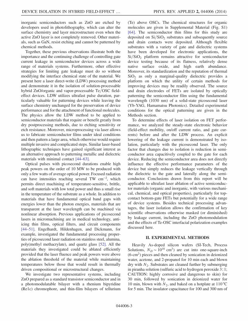
Trenches created by picosecond-laser patterning areimaged by using laser optical microscopy, scanning elec-tron microscopy (SEM), and atomic force microscopy(AFM). The images and height profiles show that the laserpatterning physically isolates transistors from the sharedsemiconductor film. The physical mechanism of the pat-terning varies for different semiconductor layers. The ZnOsemiconductor layer and SiO2 gate insulator of the ZnOFETs both have band gaps larger than the fundamental1030-nm wavelength of the Nd∶YAG picosecond laser.A large fraction of the incident optical power duringpatterning is thus transmitted to the Si substrate. In ZnO,the rapid ablation of the Si ruptures the SiO2 and ZnOlayers, creating the trenches shown in the SEM images inFig. 1. The bottoms of the trenches in Si exhibit a pattern ofridges consistent with interface instabilities observed inrapid solidification of laser-melted Si [57,58].The mechanism for laser patterning and subsequent
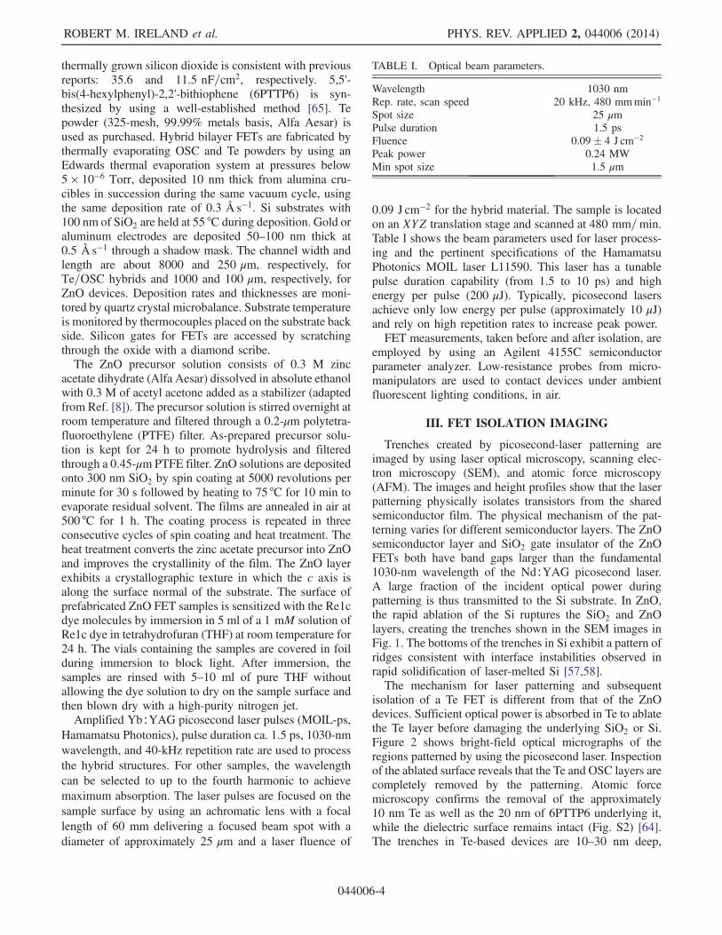
isolation of a Te FET is different from that of the ZnOdevices. Sufficient optical power is absorbed in Te to ablatethe Te layer before damaging the underlying SiO2 or Si.Figure 2 shows bright-field optical micrographs of theregions patterned by using the picosecond laser. Inspectionof the ablated surface reveals that the Te and OSC layers arecompletely removed by the patterning. Atomic forcemicroscopy confirms the removal of the approximately10 nm Te as well as the 20 nm of 6PTTP6 underlying it,while the dielectric surface remains intact (Fig. S2) [64].The trenches in Te-based devices are 10–30 nm deep,
TABLE I. Optical beam parameters.
Wavelength 1030 nmRep. rate, scan speed 20 kHz, 480 mmmin−1Spot size 25 μmPulse duration 1.5 psFluence 0.09� 4 J cm−2Peak power 0.24 MWMin spot size 1.5 μm
ROBERT M. IRELAND et al. PHYS. REV. APPLIED 2, 044006 (2014)
044006-4
which is the approximate thickness of semiconductorstacks. The edge roughness is less than 1 μm, and burrsare not apparent on the Te surface. It is therefore relativelystraightforward to remove Te films selectively at lowablation thresholds without damaging the SiO2 dielectric.The width of fabricated channels matches the diameter of
the pulse beam in the case of Te-based devices, 25 μm, andis thinner for zinc-oxide-based devices, 10 μm. In bothcases, some of the material removed from the trenches isdeposited as submicron debris in the surrounding areas.Channel widths obtained by hand isolation, via scribingaround devices with hard tools or using paint brushescarrying solvent, could not be reduced below 100 μm dueto the width of the scribing tools.
IV. FET ANALYSIS AND DISCUSSION
FET device parameters such as field-effect mobility (μ),threshold voltage (V th), gate current (IG), and the ratio ofon-to-off drain current (Ion=Ioff ) are measured as a function
of the applied gate voltage (VG) and source-drain voltage(VSD) before and after isolation. Tables SI and SII of theSupplemental Material [64] list the performance parametersof all FETs before and after the LDW method and afterscribing for comparison. Identical control devices arestored for the same time interval but do not undergoisolation. The electronic effects of hand isolation areessentially reproduced by the LDW method. Isolation byeither method reduces IG while not altering the criticalparameters, such as field-effect mobility μ and Ion=Ioff .Figure 3(a) shows graphically that the critical FET param-eters are essentially unchanged by the LDW method forzinc-oxide-and tellurium-based devices. IG of FETs in boththe on and off operation are shown separately in Fig. 3(b)for zinc-oxide- and tellurium-based devices.We observe that all parameters (mobility, on/off ratio,
and gate currents) depend on the semiconductor materialand that isolation treatment affects the gate current only byreducing it to a minimal value. The final gate leakagecurrents depend on the parasitic source-gate and drain-gate
FIG. 2. Color optical microscope images show microchannels in (a) Te (the inset shows channels in Te alongside the gold electrodepair) and (b) Te/6PTTP6.
FIG. 1. Scanning electron micrographs of (a) a laser-isolated microchannel running up to the freshly cleaved edge of the Si=SiO2=ZnOchip (scale bar 10 μm) and (b) magnification of the previous region near the edge (scale bar 2 μm).
DEVICE ISOLATION IN HYBRID FIELD-EFFECT … PHYS. REV. APPLIED 2, 044006 (2014)
044006-5

overlap and on the number of defects or pinholes in thedielectric that remain in the gate stack after isolationtreatment.
A. Zinc-oxide-based FETs
ZnO forms n-channel accumulation mode transistors.After the LDW method, the measured IG is reduced in theoff mode by almost 2 orders of magnitude [Fig. 3(b)]. Thereis still relatively large leakage in ZnO devices at high gatevoltages (50 V), which may be due to leakage at high fieldsin the regions directly beneath the source (S) and drain (D)electrodes or the FET channel.Figure 4 shows the transfer curves and IG for ZnO
devices before and after isolation, with VSD ¼ 5 and 50 V.The drain current is enhanced by isolation due to fewercurrent losses by leakage, which accounts for the slightdecrease in the on/off ratio [Fig. 3(a)]. Figure 4 also showsthat dielectric breakdown occurs after applying a gate
voltage of 40 V or higher but that isolation minimizesgate leakage over the rest of the gate voltage range. IG foron-mode ZnO devices is greater after isolation according toFig. 3(b) only because the value used is taken atVG ¼ 50 V, whereas the IG due to isolation is actuallymuch lower for applied gate voltages below the dielectricbreakdown. This difference is understandable, becauseisolation does not reduce vertical leakage current fromthe gate drain and source overlap, which would increasedrastically during dielectric breakdown as observed. TheLDW method only reduces lateral currents due toan extended semiconductor film gate stack and verticalpathways beyond the gate stack.Nonchemical isolation methods are particularly useful
for ZnO devices, because chemical etching, usually withacid, can modify ZnO/molecular interfaces. The vaportransport of the etchant can result in interface modificationwithin regions of the film separated from the etched regionsup to distances of millimeters or more. The organometallicdonor Re1c can be attached to ZnO and used to donateelectrons to ZnO following optical excitation [36]. Here weillustrate the importance of nonchemical isolation by ex-amining the photocurrent response for Re1c-functionalizedZnO FETs that are isolated by laser ablation and compare tocontrol devices which are not isolated. The drain and gatecurrents are measured in the dark and then again afterexposing the FET channel to light (λ ¼ 532 nm) for 60 s.Prior to isolation, the leakage current is on the same orderof magnitude as the drain current (greater than 5 μA at agate voltage of 30 V), as expected because the relativelyhigh mobility in the ZnO layer allows leakage current froma large area of the dielectric to contribute. The leakage IG isgreater than the photocurrent by a factor of 4 under thisforward bias condition (VG ¼ 30 V). After the isolation viathe LDW process, the magnitude of the IG is reduced to lessthan 1% of the magnitude of the photocurrent. Figure 5shows the ratio of IG to photocurrent for devices that are notisolated and devices isolated by the LDWmethod. Figure 6shows the transfer curves and IG for ZnO=Relc deviceswith and without isolation. The isolation procedure couldgreatly enhance the possibilities for use of organic-inorganic hybrids for photodetector applications.As an alternative to the LDW method, FET devices can
be isolated by locally etching the ZnO films with a mildacid, such as acetic acid. Chemical isolation using aceticacid and a paint brush is more effective than laserprocessing for eliminating gate leakage in zinc-oxide films(reduced more than 5 orders of magnitude; Fig. S3 [64]).This effectiveness could be due to the fact that the excessZnO semiconductor material is removed from around andbetween FETs, while the underlying SiO2 gate dielectric isundamaged by the comparatively mild acid etching.However, vapors from the acetic acid etching processcan uncontrollably change the conductivity of the ZnOfilm remaining in the channel, as well as possibly affect
FIG. 3. Comparison chart for (a) field-effect mobility (left axis)and on/off current ratio (right axis) and (b) gate current in the onmode (left axis) and off mode (right axis) for zinc-oxide,tellurium-based, and organic semiconductor devices. Valuesfor identical sample sets are shown in vertically aligned points;sample sets are labeled above from left to right; each point is anaverage of 12 devices. “Before” and “after” refer to measure-ments taken before and after laser isolation; values are given forboth nonisolated and “isolated” sample sets. The lower value ofred diamond and blue triangle values (compared to red square andblue circle values, respectively) for isolated systems indicates thebeneficial effect of the isolation.
ROBERT M. IRELAND et al. PHYS. REV. APPLIED 2, 044006 (2014)
044006-6

attachment of donor molecules on the surface by blockingattachment sites for the carboxylic acid groups [33].Additionally, this form of hand isolation for researchdevices is not scalable as a high-throughput isolationmethod for manufacturing arrays of many devices.
B. Tellurium and organic-based FETs
Elemental tellurium behaves as a p-channel depletionmode transistor, which means the FET is inherently on atzero VG and requires positive VG to turn the device off.The gate voltage required to turn off FETs is approximately40–50 V for our 10 nm of Te deposited at a rate of 0.3 Å s−1onto SiO2 substrates held at 60 °C. 6PTTP6 is alsop-channel and is deposited under the same conditions.6PTTP6, however, operates in accumulation and requiresonly negative VG. The drain voltage (VD) for all 6PTTP6and Te devices is swept from 0 to −20 V for measuringoutput curves and held at −20 V for transfer curves.6PTTP6 devices that are not isolated show a slight
increase in off-state IG over time [Fig. 3(b)], while the on-state IG is constant. Laser isolation reduces IG significantlyfor both cases and does so more effectively than mechanicalisolation (Table SII [64]), even though there is the pos-sibility that laser processing may eject positive Si ions fromthe oxide and could cause a buildup of electrical charge[59,62]. In Te FETs, IG is drastically reduced (4 orders ofmagnitude) by sandwiching an OSC layer between Te andthe dielectric, and lateral field-effect mobility is enhanced
by the OSC, as we noticed previously [28]. The isolation ofTe alone results in IG less than Te/6PTTP6 not isolated(5 orders of magnitude reduction), but the Te/6PTTP6bilayer after isolation, in the on state, had the lowest IG ofall. The transfer curves and IG for representative Te and Te/6PTTP6 devices, before and after isolation, are shown inSupplemental Material (Fig. S4 [64]). Note the lowercurrent scale for the IG plot after isolation.The data points in Fig. 3(b) show, counterintuitively, that
the on-state leakage current for nonisolated Te/6PTTP6 isconsiderably lower than for 6PTTP6 alone, even though theTe could greatly expand the area over which leakage couldoccur because of its much higher conductivity than that of6PTTP6. It is not clear from the data whether this effect isbecause of an attribute of the entire film area or of a fewdistributed defective points. The fact that the lower bilayeron-state leakage current is observed in a set of isolateddevices as well is evidence for this difference beingcharacteristic of the entire film, since the effect is observedat multiple arbitrary locations. This conclusion could not bereached without the isolation procedure.Note that the off-state IG is not lower for the bilayer. We
attribute this contrast to a polarity resulting from holetransfer between Te and 6PTTP6 resulting in an interfacialdipole with the positive end at Te and the negative end at6PTTP6 [28]. This polarity reflects depletion of holes in the6PTTP6, and the on-state gate-to-source voltage, with thegate more negative, would deplete these holes further, and
FIG. 4. Transfer curves and IG for ZnO devices before and after isolation, with VSD equal to (a) 5 and (b) 50 V.
DEVICE ISOLATION IN HYBRID FIELD-EFFECT … PHYS. REV. APPLIED 2, 044006 (2014)
044006-7

IG would decrease. On the other hand, the off-state voltage,where the gate is positive, would reinject holes into the6PTTP6 and IG would increase. A similar current-blockingeffect is observed for interfaces between Te and aluminumdue to diffusion of oxygen through Te grain boundaries andto the semiconductor-metal interface [63]. Injection barrierscommonly form due to chemical defects or oxidationbetween conjugated organic semiconductors and metals,particularly from metals deposited onto OSCs by vapor, butthe barriers are typically difficult to observe due to low bulkcurrents in OSCs [66–69]. In terms of applications, theisolation procedure is clearly helpful in enabling the useof field-effect devices made from low band gap or extrinsi-cally conductive semiconductors.
V. CONCLUSIONS
Isolation is critically important for devices where sensi-tivity and a high signal-to-noise ratio at low power arerequired. LDW methods are extremely reproducible, andnegligible variation in microstructural (i.e., trench depth,line-edge roughness) or FET parameters (i.e., field-effect μ)is observed between samples. Gate leakage is significantlyreduced by the LDW method for the devices that weexamine here, at least by the geometric area reduction of2–3 orders of magnitude. The LDW method is shown to bean effective alternative for removing selected domains ofboth soft semiconductors and metal oxides of certain
FIG. 6. Transfer curves for photomodulatable ZnO FETswith gate leakage, for devices without and with isolation.
FIG. 5. Linear plot and log plot of measured gate leakage tophotocurrent ratio in a representative ZnO=Relc FET. Solidcurves are for the sample isolated by the laser; dot-dashed curvesare for not isolated.
ROBERT M. IRELAND et al. PHYS. REV. APPLIED 2, 044006 (2014)
044006-8
relative hardness compared to that of the dielectric, a usefulalternative for materials that can be easily damaged byphotolithography and chemical etchants. The measuredphotocurrent for ZnO devices functionalized with donormolecules is initially masked by significant gate leakagecurrent, and that photocurrent is substantially enhanced bythe donor as deposited. Similarly, we emphasize thatremoving parasitic currents allows us to more clearlyobserve effects and behavior of the intrinsic dipole dueto energy alignment of Te-OSC heterojunctions.The preservation of lifetime characteristics, yield, and
performance for devices using semiconductors other thanSi will be driven by processing solutions which limitadverse thermal and chemical effects, while providingautomation and high-volume scaling. The LDW methodcan be automated and is scalable, because successive beamsplitters can be used to simultaneously pattern multiplearrays of circuits in parallel [70]. Ultrafast pulses allow fornoninvasive and selective material ablation, ensuring aclean and precise isolation technique which improves FETelectrical performance and eases FET performance assess-ment, thus making the LDW method a viable patterningalternative.
ACKNOWLEDGMENTS
We thank Patricia McGuiggan and Josué F. MartínezHardigree for assistance with AFM measurements. We aregrateful for the following project funding: National ScienceFoundation Division of Materials Research (DMR),MRSEC program, Grant No. 1121288 (ZnO interfaceand photocurrent), and the Department of Energy, Officeof Science, Basic Energy Sciences, Grant No. DE-FG02-07ER46465 (organic interface and tellurium work). Wethank Professor Padma Gopalan for supplying the organo-metallic dye. H. E. K., R. M. I., and Y. L. made transistordevices and acquired and analyzed I-V data under variousconditions. J. W. S. and P. G. E. made ZnO devices,attached and synthesized dye, and measured currentsincluding photocurrents. S. J., K. F., and S. O. performedlaser-isolation experiments.
[1] G. Horowitz, Organic field-effect transistors, Adv. Mater.10, 365 (1998).
[2] B. Crone, A. Dodabalapur, Y. Y. Lin, R. W. Filas, Z. Bao,A. LaDuca, R. Sarpeshkar, H. E. Katz, and W. Li, Large-scale complementary integrated circuits based on organictransistors, Nature (London) 403, 521 (2000).
[3] C. D. Dimitrakopoulos and P. R. L. Malenfant, Organic thinfilm transistors for large area electronics, Adv. Mater. 14, 99(2002).
[4] T. Someya, T. Sekitani, S. Iba, Y. Kato, H. Kawaguchi, andT. Sakurai, A large-area, flexible pressure sensor matrixwith organic-field-effect transistors for artificial skin appli-cations, Proc. Natl. Acad. Sci. U.S.A. 101, 9966 (2004).
[5] G. H. Gelinck et al., Flexible active-matrix displays andshift registers based on solution-processed organic transis-tors, Nat. Mater. 3, 106 (2004).
[6] K. Nomura, H. Ohta, A. Takagi, T. Kamiya, M. Hirano, andH. Hosono, Room-temperature fabrication of transparentflexible thin-film transistors using amorphous oxide semi-conductors, Nature (London) 432, 488 (2004).
[7] V. Subramanian, J. M. J. Frechet, P. C. Chang, D. C. Huang,J. B. Lee, S. E. Molesa, A. R. Murphy, and D. R. Redinger,Progress towards development of all-printed RFID tags:Materials, processes, anddevices, Proc. IEEE93, 1330 (2005).
[8] L. Torsi, G. M. Farinola, F. Marinelli, M. C. Tanese, O. H.Omar, L. Valli, F. Babudri, F. Palmisano, P. G. Zambonin,and F. Naso, A sensitivity-enhanced field-effect chiralsensor, Nat. Mater. 7, 412 (2008).
[9] S. H. Ko, I. Park, H. Pan, N. Misra, M. S. Rogers,C. P. Grigoropoulos, and A. P. Pisano, ZnO nanowirenetwork transistor fabrication on polymer substrate bylow-temperature, all-inorganic nanoparticle solution proc-ess, Appl. Phys. Lett. 92, 154102 (2008).
[10] C. S. Li, Y. N. Li, Y. L. Wu, B. S. Ong, and R. O. Loutfy,Fabrication conditions for solution-processed high-mobilityZnO thin-film transistors, J. Mater. Chem. 19, 1626 (2009).
[11] J. Sun, B. Zhang, and H. E. Katz, Materials for printable,transparent, and low-voltage transistors, Adv. Funct. Mater.21, 29 (2011).
[12] B. D. Ahn, H. J. Jeon, and J. S. Park, Effects of Ga:Naddition on the electrical performance of zinc tin oxide thinfilm transistor by solution-processing, ACS Appl. Mater.Interfaces 6, 9228 (2014).
[13] I. Mejia, A. L. Salas-Villasenor, A. Avendano-Bolivar, J.Horvath, H. Stiegler, B. E. Gnade, and M. A. Quevedo-Lopez, Low-temperature hybrid CMOS circuits based onchalcogenides and organic TFTs, IEEE Electron DeviceLett. 32, 1086 (2011).
[14] B. M. Dhar, R. Özgün, T. Dawidczyk, A. Andreou, andH. E. Katz, Threshold voltage shifting for memory andtuning in printed transistor circuits, Mater. Sci. Eng. R 72,49 (2011).
[15] Hagen Klauk, in Proceedings of the IEEE Device ResearchConference Organic Complementary Circuits—Scalingtowards Low Voltage and Submicron Channel Length(IEEE, University Park, 2012), pp. 41–45.
[16] W. Huan, W. Zhigong, F. Jun, L. Wenyuan, W. Rong, andM. Peng, A pixel circuit with reduced switching leakage foran organic-light-emitting diode, J. Semicond. 33, 125006(2012).
[17] A. K. Rana, N. Chand, and V. Kapoor, Gate leakage awareoptimal design of modified hybrid nanoscale MOSFET andits application to logic circuits, Iran. J. Electr. Electron. Eng.7, 112 (2011).
[18] W. Xu and S. W. Rhee, Compromise of electrical leakageand capacitance density effects: A facile route for highmobility and sharp subthreshold slope in low-voltageoperable organic filed-effect transistors, J. Mater. Chem.21, 998 (2011).
[19] C. M. Keum, J. H. Bae, M. H. Kim, W. Choi, and S. D. Lee,Solution-processed low leakage organic field-effect transis-tors with self-pattern registration based on patterneddielectric barrier, Org. Electron. 13, 778 (2012).
DEVICE ISOLATION IN HYBRID FIELD-EFFECT … PHYS. REV. APPLIED 2, 044006 (2014)
044006-9
[20] K. Rana, N. Chand, and V. Kapoor, Gate leakage reductionthrough the use of a gate-to-source/drain non-overlappedmetal-oxide-semiconductor field-effect transistor structure,J. Nanoeng. Nanosyst. 224, 173 (2010).
[21] T. Zaki, R. Rodel, F. Letzkus,H.Richter,U. Zschieschang,H.Klauk, and J. N. Burghartz, AC characterization of organicthin-film transistors with asymmetric gate-to-source andgate-to-drain overlaps, Org. Electron. 14, 1318 (2013).
[22] K. C. Dickey, S. Subramanian, J. E. Anthony, L. H. Han, S.Chen, and Y. L. Loo, Large-area patterning of solution-processable organic semiconductor to reduce parasiticleakage and off currents in thin-film transistors, Appl. Phys.Lett. 90, 244103 (2007).
[23] H. Jia, G. K. Pant, E. K. Gross, R. M. Wallace, and B. E.Gnade, Gate induced leakage and drain current offsetin organic thin film transistors, Org. Electron. 7, 16(2006).
[24] J. F. Conley, Instabilities in amorphous oxide semiconductorthin-film transistors, IEEE Trans. Device Mater. Reliab. 10,460 (2010).
[25] S. Hengen, M. Alt, G. Hernandez-Sosa, J. Giehl, U.Lemmer, and N. Mechau, Modelling and simulation ofgate leakage currents of solution-processed OTFT, Org.Electron. 15, 829 (2014).
[26] J. F. M. Hardigree, T. J. Dawidczyk, R. M. Ireland, G. L.Johns, B. J. Jung, M. Nyman, R. Osterbacka, N. Markovic,and H. E. Katz, Reducing leakage currents in n-channelorganic field-effect transistors using molecular dipolemonolayers on nanoscale oxides, ACS Appl. Mater.Interfaces 5, 7025 (2013).
[27] B. J. Jung, J. F. M. Hardigree, B. M. Dhar, T. J. Dawidczyk,J. Sun, K. C. See, and H. E. Katz, Naphthalenetetracarbox-ylic diimide layer-based transistors with nanometer oxideand side chain dielectrics operating below one volt, ACSNano 5, 2723 (2011).
[28] R. M. Ireland, T. J. Dawidczyk, P. Cottingham, T. McQueen,G. Johns, N. Markovic, L. Zhang, P. Gopalan, and H. E.Katz, Effects of pulsing and interfracial potentials ontellurium-organic heterostructured film, ACS Appl. Mater.Interfaces 5, 1604 (2013).
[29] S. Kobayashi, T. Nishikawa, T. Takenobu, S. Mori, T.Shimoda, T. Mitani, H. Shimotani, N. Yoshimoto, S.Ogawa, and Y. Iwasa, Control of carrier density by self-assembled monolayers in organic field-effect transistors,Nat. Mater. 3, 317 (2004).
[30] P. Paoprasert, B. Park, H. Kim, P. Colavita, R. J. Hamers,P. G. Evans, and P. Gopalan, Dipolar cromophore functionallayers in organic field-effect transistors, Adv. Mater. 20,4180 (2008).
[31] B. Park, S. Choi, S. Graham, and E. Reichmanis, Memoryand photovoltaic elements in organic filed-effect transistorswith donor/acceptor planar-hetero junction interfaces,J. Phys. Chem. C 116, 9390 (2012).
[32] Bo Zhang, Y Liu, S. Agarwal, M. L. Yeh, and H. E. Katz,Structure, sodium ion role, and practical issues for beta-alumin as high-k dielectric solution-processed gate layer fortransparent low-voltage electronics, ACS Appl. Mater.Interfaces 3, 4254 (2011).
[33] J. W. Spalenka, P. Gopalan, H. E. Katz, and P. G. Evans,Electron mobility enhancement in ZnO thin films via
surface modification by carboxylic acids, Appl. Phys. Lett.102, 041602 (2013).
[34] P. Paoprasert, J. E. Laaser, W. Xiong, R. A. Franking,R. J. Hamers, M. T. Zanni, J. R. Schmidt, and P. Gopalan,Bridge-dependent interfacial electron transfer fromrhenium-bipyridine complexes to TiO2 nanocrystalline thinfilms, J. Phys. Chem. C 114, 9898 (2010).
[35] P. Paoprasert, S. Kandala, D. P. Sweat, R. Ruther, and P.Gopalan, Versatile grafting chemistry for creation of stablemolecular layers on oxides, J. Mater. Chem. 22, 1046(2012).
[36] J. W. Spalenka, Y. Joo, R. M. Ireland, P. Gopalan, H. E.Katz, and P. G. Evans (unpublished).
[37] B. N. Pal, B. M. Dhar, K. C. See, and H. E. Katz, Solution-deposited sodium beta-alumina gate dielectrics for low-voltage and transparent field-effect transistors, Nat. Mater.8, 898 (2009).
[38] Y. Su, C. Wang, W. Xie, F. Xie, J. Chen, N. Zhao, and J. Xu,Low-voltage organic field-effect transistors with solution-processed metal-oxide as gate dielectric, ACS Appl. Mater.Interfaces 3, 4662 (2011).
[39] Y. M. Park, A. Desai, and A. Salleo, Solution-processsablezirconium oxide gate dielectrics for flexible organic fieldeffect transistors operated at low voltages, Chem. Mater. 25,2571 (2013).
[40] J. Peng, Q. Sun, S. Wang, H. Q. Wang, and W. Ma, Low-temperature solution-processed alumina as gate dielectricfor reducing the operating-voltage of organic field-effecttransistors, Appl. Phys. Lett. 103, 061603 (2013).
[41] R. P. Ortiz, A. Fachetti, and T. J. Marks, High-k organic,inorganic, and hybrd dielectrics for low-voltage organicfield-effect transistors, Chem. Rev. 110, 205 (2010).
[42] J. Veres, S. D. Ogier, S. W. Leeming, D. C. Cupertino, andS. M. Khaffaf, Low-k insulators as the choice of dielectricsin organic field-effect transistors, Adv. Funct. Mater. 13, 199(2003).
[43] P. F. Moonen, I. Yakimets, and J. Huskens, Fabrication oftransistors on flexible substrates: from mass-printing tohigh-resolution alternative lithography strategies, Adv.Mater. 24, 5526 (2012).
[44] P. Tormala, T. Pohjonen, and P. Rokkanen, Bioabsorbablepolymers: Materials technology and surgical applications,J. Eng. Med. 212, 101 (1998).
[45] D. Analdo del Cerro, G. R. B. E. R. Omer, and A. J. HuisVeld, Picosecond laser machined designed patterns withanti-ice effect, in Proceedings of the Eleventh InternationalSymposium on Laser Precision Microfabrication, Stuttgart,2010 (Japan Laser Processing Society, Osaka, 2010).
[46] M. D. Perry, B. C. Stuart, P. S. Banks, M. D. Feit, V.Yanovsky, and A. M. Rubenchik, Ultrashort-pulse lasermachining of dielectric materials, J. Appl. Phys. 85, 6803(1999).
[47] V. V. Rana and Z. Zhang, Selective removal of dielectriclayers using picosecond UV pulses, in Proceedings of theSPIE Conference on Solid State Lasers XVIII: Technologyand Devices, San Jose, 2009 (SPIE, Bellingham,WA, 2009).
[48] J. Kruger, M. Lenzner, S. Martin, M. Lenner, C. Spielmann,A. Fiedler, and W. Kautek, Single- and multi-pulse femoto-second laser ablation of optical filter materials, Appl. Surf.Sci. 208–209, 233 (2003).
ROBERT M. IRELAND et al. PHYS. REV. APPLIED 2, 044006 (2014)
044006-10
[49] F. Haase, E. G. Rojas, K. Bothe, and R. Brendel, Layerselective laser ablation for local contacts to thin emitters,Energy Procedia 8, 577 (2011).
[50] R. Mandamparambil, H. Fledderus, G. Van Steenberge, andA. Dietzel, Patterning of Flexible Organic Light EmittingDiode (FOLED) stack using an ultrafast laser, Opt. Express18, 7575 (2010).
[51] J. Bonse, G. Mann, J. Kruger, M. Marcinkowski, and M.Eberstein, Femtosecond laser-induced removal of siliconnitride layers from doped and textured silcon wafers used inphotovoltaics, Thin Solid Films 542, 420 (2013).
[52] U. Engelhardt, J. Hildenhagen, and K. Dickmann, Micro-machining using high-power picosecond lasers: comparisonof various materials, Laser Tech. J. 8, 32 (2011).
[53] P. Balling and J. Schou, Femtosecond-laser ablationdynamic of dielectrics: Basics and applications for thinfilms, Rep. Prog. Phys. 76, 036502 (2013).
[54] C. Momma, S. Nolte, B. N. Chichkov, F. v. Alvensleben,and A. Tunnermann, Precise laser ablation with ultrashortpulses, Appl. Surf. Sci. 109–110, 15 (1997).
[55] G. Raciukaitis, M. Brikas, M. Gedvilas, and G. Darcianovas,Patterning of ITO layer on glass with high repetitionrate picosecond lasers, J. Laser Micro/Nanoeng. 2, 1(2007).
[56] A. Ben-Yakar and R. L. Byer, Femtosecond laser machiningof fluidic microchannels for miniaturized bioanalyticalsystems, in Proceedings of the SPIE (SPIE, Bellingham,WA, 2002).
[57] Y. F. Lu, W. K. Choi, Y. Aoyagi, A. Kinomura, and K. Fujii,Controllable laser-induced periodic structures at silicon-dioxide/silicon interface by excimer laser irradiation,J. Appl. Phys. 80, 7052 (1996).
[58] A. J. Pedraza, Y. F. Guan, J. d. Fowlkes, and D. A.Smith, Nanostructures produced by ultraviolet laserirradiation of silicon, J. Vac. Sci. Technol. B 22, 2823(2004).
[59] N. M. Bulgakova, R. Stoian, A. Rosenfeld, I. V. Hertel, andE. E. B. Campbell, Electronic transport and consequencesfor material removal in ultrafast pulsed laser ablation ofmaterials, Phys. Rev. B 69, 054102 (2004).
[60] A. Tunnermann, S. Nolte, and J. Limpert, Femtosecond vs.picosecond material processing: Challenges in ultrafast
precision laser micro-machining of metals at high repetitionrates, Laser Tech. J. 7, 34 (2010).
[61] J. Cheng, C. S. Liu, S. Shang, D. Liu, W. Perrie, G. Dearden,and K. Watkins, A review of ultrafast laser materialsmachining, Opt. Laser Technol. 46, 88 (2013).
[62] R. Stoian, A. Rosenfeld, D. Ashkenasi, I. V. Hertel, N. M.Bulgakova, and E. E. B. Campbell, Surface chargingand impulsive ion ejection during ultrashort pulsed laserablation, Phys. Rev. Lett. 88, 097603 (2002).
[63] N. M. Bulgakova, A. V. Bulgakov, V. P. Zhukov, W. Marine,A. Y. Vorobyev, and C. Guo, Charging and plasma effectsunder ultrashort pulsed laser ablation, in Proceedings of theSPIE Conference on High-Power Laser Ablation VII, Taos,2008 (SPIE, Bellingham, WA, 2008).
[64] See Supplemental Material at http://link.aps.org/supplemental/10.1103/PhysRevApplied.2.044006 forchemical structures, an AFM of a trench ablation, andadditional gate current plots.
[65] H. E. Katz, T. Siegrist, M. Lefenfeld, P. Gopalan, M.Mushrush, B. Ocko, O. Gang, and N. Jisrawl, Mesophasetransitions, surface functionalization, and growth mecha-nism of semiconducting 6PTTP6 films from solution,J. Phys. Chem. B 108, 8567 (2004).
[66] K. Okuyama, J. Tsuhako, and Y. Kumagai, Behavior ofmetal contacts to evaporated tellurium films, Thin SolidFilms 30, 119 (1975).
[67] H. Ishii, K. Sugiyama, E. Ito, and K. Seki, Energy levelalignment and interfacial structures at organic/metal andorganic/organic interfaces, Adv. Mater. 11, 605 (1999).
[68] A. Crispin, A. Jonsson, M. Fahlman, and W. R. Salaneck,Aluminum-barium interfaces on some processablepoly(p-phenylene vinylene) polymers studied by photo-electron spectroscopy, J. Chem. Phys. 115, 5252(2001).
[69] J. Hwang, A. Wan, and A. Kahn, Energetics of metal-organic interfaces: New experiments and assessment of thefield, Mater. Sci. Eng. R 64, 1 (2009).
[70] Z. Kuang, W. Perrie, D. Liu, S. P. Edwardson, Y. Jiang, E.Fearon, K. G. Watkins, and G. Dearden, Ultrafast laserparallel microprocessing using high uniformity binaryDammann grafting generated beam array, Appl. Surf. Sci.273, 101 (2013).
DEVICE ISOLATION IN HYBRID FIELD-EFFECT … PHYS. REV. APPLIED 2, 044006 (2014)
044006-11