development of ultra-compact optical transceivers for iot ... · silicon photonics technology...
TRANSCRIPT
1 OKI Technical Review May 2017 / Issue 229 Vol. 84 No.1
Hiroki Yaegashi
In the era of Internet of Things (IoT) where every “thing” is connected to the Internet, constructing a network to accommodate the vast flow of data is an urgent matter. The access network anticipated to support IoT is the 5th generation mobile network (5G mobile) currently undergoing standardization. In the mobile network, the required communication capacity of the backhaul optical lines that connect base stations with the core network is predicted to increase more and more as time goes by. Additionally, for the fronthaul connecting the 5G mobile base stations with the large number of small cell antennas, accommodation of a low-cost network configuration in an existing optical access network is being studied. This requires incorporating an optical interface into the small antenna device, therefore miniaturization of the optical transceiver is indispensable.
Silicon photonics technology enables manufacturing of ultra-compact optical circuits at low cost. When this technology is applied to the optical transceiver of an optical access network, optical devices such as optical transmitter, photodetector and wavelength multiplexing/demultiplexing filter constituting an optical transceiver can be integrated on a single silicon chip. Thus, the transceiver can be miniaturized an order of magnitude smaller, which also leads to lower power consumption, and cost can be reduced due to the greatly simplified assembly process.
As a member company of the Photonics Electronics Technology Research Association (PETRA), OKI is participating in the “Integrated Photonics-Electronics
Convergence System Technology” project commissioned by the New Energy and Industrial Technology Development Organization (NEDO) to develop an ultra-compact optical transceiver utilizing silicon photonics for IoT networks. This article provides an overview of the development.
Overview of “Integrated Photonics-Electronics Convergence System Technology” project
“Integrated Photonics-Electronics Convergence System Technology” project was started in September 2012 as part of the Ministry of Economy, Trade and Industry’s “Future Pioneering Projects” , and since 2013, the project has been undertaken and commissioned out by NEDO. The aim is to establish a basic technology that will realize optoelectronic packaging system technology, which integrates optical wiring technology and electronic circuit technology to convert electrical wirings of electronic equipment to optical fibers enabling energy savings and speed-up of information communication equipment. Based on optoelectronic integration technology, development of energy-saving technologies for server systems in data centers and IT equipment in optical communication
systems are being promoted.
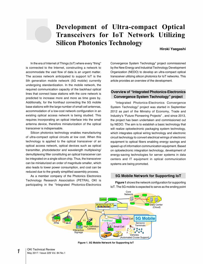
5G Mobile Network for Supporting IoT
Figure 1 shows the network configuration for supporting IoT. The 5G mobile is expected to serve as the ending point
Figure 1. 5G Mobile Network for Supporting IoT
5G Mobile
Interactive Signage
High Definition Camera
Multichannel OLT
Control Edge
Core Network
Data Center (Cloud)
Sensors/Terminals
Vehicles (Automated Cruise Support)
Fronthaul
Small Cell
Small Cell
Development of Ultra-compact Optical Transceivers for IoT Network Utilizing Silicon Photonics Technology

2OKI Technical Review May 2017 / Issue 229 Vol. 84 No.1
of the IoT network connected to the enormous number of sensors and terminals. According to the 5G mobile standards, the terminal communication speed is increased to a maximum of 10Gbps, the subdivided antenna areas (small cells) are arranged about 100 times denser than in previous mobile networks, and connection of about 1 million terminals per square kilometer is assumed.
Various schemes are being studied for the fronthaul network that connects the large number of small cell antennas. Among them, the scheme to accommodate the small cell antennas in an existing optical access network using a passive optical network (PON) configuration is promising from the viewpoint of cost.
PON is a network configuration that splits the optical fiber connecting the base station and subscribers into a point-to-multipoint connection using time multiplexing. Since the base station equipment and the optical fiber line are shared by multiple subscribers, the facility cost of the network can be kept low. The optical termination devices on the base station side and the subscriber side are called Optical Line Terminal (OLT) and Optical Network Unit (ONU), respectively. In the fronthaul configuration using PON, ONU is incorporated in each small cell antenna.
To accommodate the communication capacity of 5G mobile, Time and Wavelength Division Multiplexing-PON (TWDM-PON), which combines PON with wavelength multiplexing, is used. TWDM-PON is defined in ITU-T G.989 series standards, and the configuration is outlined in Figure 2. The scheme is a single-fiber bi-directional communication over a single-mode optical fiber using the 1524-1544nm wavelength band in the uplink (subscriber to base station) direction and 1596-1603nm wavelength band in the downlink (base station to subscriber) direction. The up and down links are multiplexed with four wavelength each, and at 10Gbps per wavelength, it provides a total communication of 40Gbps.
Figure 2. TWDM-PON Configuration
4 Wavelength Multiplexing
(100GHz Interval)
Base Station Side Subscriber Side
Max. 256 Branches
10Gbps/ch
Ultra-compact Optical Transceiver utilizing Silicon Photonics
Conventional ONU is a desktop-size device and cannot be fitted as is into a 5G mobile’s small cell antenna. A small
optical transceiver is essential in order to compact the ONU for incorporation into a small cell antenna. Hence, the goal is to development a SFP+1) size (power consumption of 1.5 W or less) ultra-compact optical transceiver for the TWDM-PON ONU.
The ONU optical transceiver consists of a single-fiber bi-directional optical transceiver module and its driving circuit. The single-fiber bi-directional optical transceiver module has conventionally been assembled by putting together individual components such as optical transmitter, optical receiver and wavelength multiplexing/demultiplexing filter.
OKI has been developing ultra-compact optical transceivers using silicon photonics2). Figure 3 shows the configuration of a single-fiber bi-directional optical transceiver chip for the TWDM-PON ONU (hereinafter called the optical transceiver chip) that is currently under development.
Figure 3. Configuration of Optical Transceiver Chip for TWDM-PON ONU
LD Array
PD Array
Functions required in the optical transceiver chip are a function to select and transmit one wavelength out of the four transmission wavelengths, and a function to select and receive one wavelength from the four multiplexed wavelengths of randomly polarized input light.
The transmitted light from a laser diode(LD) array passes through an upstream wavelength division multiplexing filter (WDM2), an optical modulator (Mod), an upstream/downstream wavelength division multiplexer/demultiplexer filter (WDM1), and spot size converter (SSC) before being output on the optical fiber. At the exit end, the SSC enlarges the diameter of the light beam propagating through the silicon-wire waveguide up close to the diameter of the beam in the optical fiber to reduce optical coupling loss.
On the other hand, the path of the received light is a polarization diversity configuration in order to eliminate polarization dependence. From the optical fiber, the light passes through the SSC and WDM1 before going to the polarization beam splitter (PBS) where it is split into TE and TM polarized components. The TE polarized

3 OKI Technical Review May 2017 / Issue 229 Vol. 84 No.1
Figure 4(b) shows the reflection spectrum of the prototype bandpass filter. The reflection wavelength bands for incident lights of TE and TM polarizations are perfectly matched to each other, and excellent polarization-independent bandpass filter characteristic with a difference in reflectance of 0.2dB or less was obtained for both polarizations.
AWG in Figure 3 separates the wavelength of the received wavelength-multiplexed light. The element is about 1.4mm square and separates up to eight wavelengths at an optical frequency interval of 100GHz.Since the AWG itself has a remarkable polarization dependence and the design only assumes TE polarization, it is used in combination with the polarization diversity configuration in the optical transceiver chip as shown in Figure 3. Figure 5(a) is a photomicrograph of the prototype AWG4), and Figure 5(b) shows the filter spectral characteristics. OKI’s own geometric design has produced an element with a low 1.2dB loss and -16dB crosstalk between wavelengths, therefore the outlook for use in the TWDM-PON is promising.
Figure 5. Arrayed-Waveguide Grating (AWG)
Input Light Output Light
(2) Germanium PhotodetectorThe monolithic integration of germanium (Ge)
photodetector into a waveguide is one of the major advantages of using silicon photonics technology.
Figure 6 is a cross-sectional schematic of a waveguide Ge photodetector (constituting the “PD array” in Figure 3) used for the optical transceiver chip5). Through crystal growth, a Ge light absorption layer was formed on the silicon (Si) waveguide layer. It is a PIN photodiode in which the Si layer is p-type and the upper portion of the Ge layer is n-type.
The prototype Ge photodetector exhibited excellent voltage-current characteristics with extremely low dark current of 11nA at 1V reverse bias. Figure 7(a) shows the responsivity spectrum at 1V reverse bias. Almost a flat characteristic of 0.8A/W was obtained over the wavelength range of 100nm. Introduction of an avalanche photodiode
component is left as is while the TM polarized component is sent to the polarization rotation element (PR) for conversion to a TE polarized component. Both polarized components are wavelength-separated by their respective arrayed-waveguide grating (AWG) then received by the photodetector (PD) array.
Each element is connected by a silicon-wire waveguide.The LD array is a multi-striped semiconductor laser chip of four wavelengths, and one wavelength is chosen to make continuous oscillation. Although the LD array is flip-chip mounted, all other elements are monolithically integrated on the silicon chip greatly reducing assembly cost. The chip size is 5 mm × 3.5 mm that can be mounted on a SFP+ size ultra-compact optical transceiver. As a result, a compact ONU that can be incorporated in a small cell antenna can be realized at a low cost.
Among the silicon photonics elements constituting the optical transceiver chip, the wavelength multiplexing/demultiplexing filter and the germanium photodetector are introduced in next section.
Silicon Photonics Element Technology
(1) Wavelength Multiplexing/Demultiplexing FilterFigure 4(a) shows a schematic of the polarization-
independent bandpass filter, which is a component of the upstream/downstream wavelength multiplexing/demultiplexing filter (WDM1 in Figure 3)3). A polarization rotation grating and a polarization-independent 3dB coupler are combined to achieve polarization-independent operation. The antisymmetric grooves (antisymmetric grating) formed on the left and right sidewalls of the waveguide’s silicon core allows the polarization rotation grating to selectively reflect light of a specific wavelength. Furthermore, it has the function to convert the incident light’s TE and TM polarized wave components into the TM and TE polarized components of the reflected light, respectively.
Figure 4. Polarization-independent Bandpass Filter
Antisymmetric Grating
3dB Coupler
Si SubstrateSi Core
SiO2 Cladding
Polarization Rotation Grating

4OKI Technical Review May 2017 / Issue 229 Vol. 84 No.1
3) H. Okayama, et al., “Polarization rotation Bragg grating with high diffraction efficiency using Si waveguide top surface groove grating,” Electronics Letters, Vol. 51, p. 1909–1911 (2015).
4) H. Okayama, et al., “Low loss 100 GHz spacing Si arrayed-waveguide grating using minimal terrace at slab–array interface,” Electronics Letters, Vol. 52, p. 1545–1546 (2016).
5) H. Ono, et al., “Waveguide Ge-PIN-PD for GE-PON transceivers,” 2015 IEICE General Conference, C-3-56References
Authors
Hiroki Yaegashi, Network and Terminal Technologies R&D Department, Corporate Research & Development Center, Information & Technologies Planning Group
is being considered to obtain even higher responsivity. Figure 7(b) shows the frequency response characteristic. The cutoff frequency at reverse bias of 1V was 7.9GHz, and a sufficient response speed applicable to TWDM-PON was obtained.
Figure 6. Cross-sectional Schematic of Germanium Photodetector
Electrodes
SiO2 Cladding
Ge Light Absorption Layer
Si Waveguide LayerSi Substrate
Reverse Bias 1V
Figure 7. Characteristics of Prototype Germanium Photodetector
Conclusion
Development of an ultra-compact optical transceiver for 5G mobile network supporting IoT was introduced. Low loss of wavelength multiplexing/demultiplexing filter based on silicon photonics technology, improvements in germanium photodetector efficiency and ultra-compact integrated optical transceiver chip are sure to be breakthroughs in lowering power consumption and cost of the optical transceiver.
Acknowledgement
This research is partly supported by the New Energy and Industrial Technology Development Organization (NEDO).
References
Authors
1) SFF-8431 “Specifications for Enhanced Small Form Factor Pluggable Module SFP+”
http://www.sfplustransceiver.com/pdf/MSA-SFF-8431.pdf2) Y. Onawa, et al., “Development of Polarization-Independent
Silicon Waveguide Functional Devices,” OKI Technical Review Issue 219, pp. 32-37, April 2012
silicon photonics General term for an optical device technology using silicon. Conventional optical devices commonly use compound semiconductors such as gallium arsenide and indium phosphide, or dielectrics such as quartz. Using silicon as a material, miniaturization of optical devices, integration of optical devices and silicon LSI, and productivity improvement are expected.
silicon-wire waveguide Waveguide is a pathway for propagating light along a desired path. In the silicon-wire waveguide, the core is made of silicon and the cladding is made of quartz. Compared with conventionally used quartz waveguide, light is strongly confined, and it hardly leaks out even if the light path is sharply bent enabling the layout of the optical circuit to be minimized.
polarization Light is an electromagnetic field and can be considered divided into two polarization components whose oscillation directions of electromagnetic fields are orthogonal to each other. In this article, the component whose oscillation direction of electric field is parallel to the element substrate surface is called TE polarization, and the vertical component is called TM polarization.
polarization diversity Generally, the refractive index perceived by the light from the medium differs according to the state of polarization. Therefore, the characteristics of the optical device depend on the polarization state. In optical reception, polarization dependence can be eliminated as a whole through the separation of light into polarization components orthogonal to each other and adding up the signals received by the photodetectors optimized for each. This is called polarization diversity.
Glossary