development of quantitative techniques for the study of ... · development of quantitative...
TRANSCRIPT
Development of Quantitative Techniques
for the Study of Discharge Events During
Plasma Electrolytic Oxidation Processes
Christopher S. Dunleavy, Trinity College
This dissertation is submitted for the degree of Doctor of Philosophy
University of Cambridge
Department of Materials Science and Metallurgy
1

Preface.
This dissertation is submitted for the degree of Doctor of Philosophy at the Univer-
sity of Cambridge. The research described herein was carried out by myself in the
period from October 2006 to July 2010, under the supervision of Professor T.W.
Clyne, in the Department of Materials Science and Metallurgy at the University of
Cambridge.
To the best of my knowledge, the work described in this dissertation is original,
except where due reference has been made to the work of others, and includes noth-
ing which is the outcome of work done in collaboration except where specifically
indicated in the text. No part of this dissertation, or any similar to it, has been,
or is currently being submitted for any degree, or other qualification, at any other
university. It is less then 60 000 words in length.
Christopher S. Dunleavy, July 2010.
2

Development of Quantitative Techniques for the Study of Discharge Events
During Plasma Electrolytic Oxidation Processes
Christopher S. Dunleavy
Abstract.
Plasma electrolytic oxidation, or PEO, is a surface modification process for the
production of ceramic oxide coatings upon substrates of metals such as aluminium,
magnesium and titanium. Two methodologies for the quantitative study of elec-
trical breakdown (discharge) events observed during plasma electrolytic oxidation
processes were developed and are described in this work.
One method presented involves direct measurement of electrical breakdowns
during production of an oxide coating within an industrial scale PEO processing
arrangement. The second methodology involves the generation and measurement
of electrical breakdown events through coatings pre-deposited using full scale PEO
processing equipment. The power supply used in the second technique is generally
of much lower power output than the system used to initially generate the sample
coatings.
The application of these techniques was demonstrated with regard to PEO coat-
ing generation on aluminium substrates. Measurements of the probability distri-
butions of discharge event characteristics are presented for the discharge initiation
voltage; discharge peak current; event total duration; peak instantaneous power;
charge transferred by the event and the energy dissipated by the discharge.
Discharge events are shown to increase in scale with the voltage applied dur-
ing the breakdown, and correlations between discharge characteristics such as peak
discharge current and event duration are also detailed. Evidence was obtained
which indicated a probabilistic dependence of the voltage required to initiate dis-
charge events. Through the scaling behaviour observed for the discharge events,
correspondence between the two measurement techniques is demonstrated. The
complementary nature of the datasets obtainable from different techniques for mea-
surement of PEO discharge event electrical characteristics is discussed with regards
to the effects of interactions between concurrently active discharge events during
large scale PEO processing.
3

Acknowledgements.
I gratefully acknowledge the financial support of the Engineering and Physical Sci-
ences Research Council. I am also grateful for the additional funding provided
each year by the Department of Materials Science and Metallurgy. Thanks are due
also Professor A.L. Greer for provision of office, laboratory and workshop facilities
within the department. I would also like to thank Trinity College for the excellent
graduate accommodation from which I benefited greatly during my studies.
I would like to thank my supervisor Prof. T.W. Clyne for all his advice and input
to the project. In particular for his having created in the Gordon lab an environment
which is not only welcoming but also a place in which creative thinking can thrive.
Elsewhere in the department the project would not have gotten very far without
the assistance of Kevin Roberts and Les Allen, who seem to never lack for a plan
to bypass or resolve any experimental difficulties. The frequent assistance of Keith
Page and Maddy MacElroy, and their patience with my deviant requirements for
electronics with crucial to the success of the project. A good deal is owed to Keronite
Plc for the loaning of PEO processing equipment and raw materials for processing.
I was also thankful for the assistance of Simon Griggs with SEM facilities. Special
mention must be made of James Curran, for many, many useful discussions and a
surplus of mad ideas.
Within the Gordon lab many people have helped me along the way. Special
thanks go to Julien, Sandra and Erica for performing the sacred rituals of coffee
machine maintenance. The original three postdocs, Athina, Jin and Igor, now all
moved on to better things, for help settling in and getting started. Helen and Jiu
Ching for finishing before me. Andy and Sonya for hanging around the computer
room and chatting almost as much as I do. Liza for returning to study PEO despite
the detonation of her part III practical, and Maya who can understand the pain
of running long experiments on the process lab mezzanine. James Dean is just
generally a great guy to have around the lab, and naturally I could never forget
The Jeff.
Outside the lab, much appreciation is directed towards all those I’ve known
through First and Third, for all the cold mornings,maths chat and mighty victories.
Long suffering friend Steph, without whom I would be less addicted to caffeine, but
would know less of the brains of rats. I must thank the guys from MK, Jonny, Ruari
and Dave for helping me escape from Cambridge for short periods for time to time,
and Rik and Emily in London for the same. Finally Hannah for coffee, care, and
moral support throughout the thesis.
4

Contents
1 Introduction. 12
1.1 PEO processing. . . . . . . . . . . . . . . . . . . . . . . . . . . . . . 12
1.2 PEO coatings. . . . . . . . . . . . . . . . . . . . . . . . . . . . . . . 16
1.3 PEO coating applications. . . . . . . . . . . . . . . . . . . . . . . . 17
1.4 Research aims. . . . . . . . . . . . . . . . . . . . . . . . . . . . . . 18
1.5 Document overview. . . . . . . . . . . . . . . . . . . . . . . . . . . 18
2 The Plasma Electrolytic Oxidation Process. 20
2.1 Reported properties of discharge events
during plasma electrolytic oxidation. . . . . . . . . . . . . . . . . . 20
2.1.1 Experimental approaches. . . . . . . . . . . . . . . . . . . . 20
2.1.2 Durations of discharge events. . . . . . . . . . . . . . . . . . 22
2.1.3 Discharge event currents. . . . . . . . . . . . . . . . . . . . . 25
2.1.4 Spatial scale of discharge events. . . . . . . . . . . . . . . . . 26
2.1.5 Discharge event spatial density. . . . . . . . . . . . . . . . . 29
2.1.6 Discharge plasma composition. . . . . . . . . . . . . . . . . 30
2.1.7 Discharge plasma temperature. . . . . . . . . . . . . . . . . 30
2.2 Bulk electrical properties of PEO processing. . . . . . . . . . . . . . 31
2.3 Structures of PEO Coatings . . . . . . . . . . . . . . . . . . . . . . 33
2.3.1 Growth rates and thicknesses of PEO coatings. . . . . . . . 33
2.3.2 Exterior surfaces of PEO coatings. . . . . . . . . . . . . . . 33
2.3.2.1 Appearance of coating surfaces. . . . . . . . . . . . 35
2.3.2.2 Discharge channel sizes and populations. . . . . . . 35
2.3.2.3 Surface roughness of coatings. . . . . . . . . . . . . 37
2.3.3 Coating interior microstructures. . . . . . . . . . . . . . . . 39
2.3.4 Coating porosity. . . . . . . . . . . . . . . . . . . . . . . . . 41
2.3.5 Phase constitution. . . . . . . . . . . . . . . . . . . . . . . . 42
2.3.6 Elemental distributions. . . . . . . . . . . . . . . . . . . . . 45
3 Methodology. 47
5

3.1 PEO Processing Equipment. . . . . . . . . . . . . . . . . . . . . . . 47
3.2 In-situ Discharge Monitoring Experiments. . . . . . . . . . . . . . . 51
3.2.1 Variations of discharge characteristics with processing time
and effects of monitored area size. . . . . . . . . . . . . . . . 53
3.3 Single Discharge Experiments. . . . . . . . . . . . . . . . . . . . . . 55
3.3.1 Small area general set-up. . . . . . . . . . . . . . . . . . . . 56
3.3.2 Single Discharge Machine MK I. . . . . . . . . . . . . . . . . 59
3.3.3 Single Discharge Machine MK II. . . . . . . . . . . . . . . . 60
3.4 Single discharge experiments performed. . . . . . . . . . . . . . . . 61
3.4.1 Coating thickness and test circuit capacitance effects. . . . . 61
3.4.2 Generation of dataset for calibration of in-situ current probe. 63
3.5 Microscopy and sample preparation. . . . . . . . . . . . . . . . . . . 63
3.5.1 Cold mounting of samples . . . . . . . . . . . . . . . . . . . 63
3.5.2 Hot mounting of samples. . . . . . . . . . . . . . . . . . . . 64
3.5.3 Sample sectioning. . . . . . . . . . . . . . . . . . . . . . . . 64
3.5.4 Polishing procedures. . . . . . . . . . . . . . . . . . . . . . . 64
3.5.5 Optical microscopy. . . . . . . . . . . . . . . . . . . . . . . . 64
3.5.6 Scanning electron microscopy. . . . . . . . . . . . . . . . . . 65
3.6 Processing of data. . . . . . . . . . . . . . . . . . . . . . . . . . . . 65
3.6.1 Analysis of single discharge data. . . . . . . . . . . . . . . . 65
3.6.2 Analysis of in-situ monitoring data. . . . . . . . . . . . . . . 68
3.6.3 Averaged development profiles of discharge events. . . . . . . 72
4 Evolution of Discharge Events During Coating Production. 73
4.1 In-situ monitoring with scaling of monitored area. . . . . . . . . . . 73
4.1.1 Coating development on the small area. . . . . . . . . . . . . 73
4.1.2 Thickness development and surface appearance. . . . . . . . 75
4.1.3 Comparison of charge delivered to small and large areas. . . 76
4.1.4 Cumulative charge of indexed discharge events. . . . . . . . 77
4.1.5 Discharging rates. . . . . . . . . . . . . . . . . . . . . . . . . 78
4.2 Properties of individual events recorded
during in-situ monitoring of the PEO process and variation with
processing time. . . . . . . . . . . . . . . . . . . . . . . . . . . . . . 82
4.2.1 Event initiating voltages. . . . . . . . . . . . . . . . . . . . . 83
4.2.2 Discharge event peak current. . . . . . . . . . . . . . . . . . 84
4.2.3 Discharge event durations. . . . . . . . . . . . . . . . . . . . 85
4.2.4 Peak instantaneous power levels. . . . . . . . . . . . . . . . 86
4.2.5 Charge and energy of individual discharges. . . . . . . . . . 87
4.3 Small current (< 10 mA) events. . . . . . . . . . . . . . . . . . . . . 89
6

4.4 Occurrence of electrical breakdowns during cathodic polarisation of
the substrate. . . . . . . . . . . . . . . . . . . . . . . . . . . . . . . 89
5 Single Discharge Experiments. 92
5.1 Coating thickness development. . . . . . . . . . . . . . . . . . . . . 92
5.2 Discharge event resistance at peak current. . . . . . . . . . . . . . . 96
5.3 Event average properties. . . . . . . . . . . . . . . . . . . . . . . . . 97
5.4 Discharge event probability histograms. . . . . . . . . . . . . . . . . 101
5.5 Clustering behaviour of discharge events. . . . . . . . . . . . . . . . 105
5.5.1 Definition of a cluster. . . . . . . . . . . . . . . . . . . . . . 106
5.5.2 The tendency towards clustering. . . . . . . . . . . . . . . . 108
5.5.3 Likelihood of sequential events in clusters being
spatially related. . . . . . . . . . . . . . . . . . . . . . . . . 109
5.6 Relation of the initiating voltage and circuit capacitance . . . . . . 109
6 Scaling Effects for Discharge Events. 115
6.1 Correlations between initiation voltage and peak current in single
discharge data. . . . . . . . . . . . . . . . . . . . . . . . . . . . . . 115
6.2 Discharge event scaling and average current development profiles for
single discharge data. . . . . . . . . . . . . . . . . . . . . . . . . . . 121
6.3 Correlations between initiation voltage and event duration in single
discharge data. . . . . . . . . . . . . . . . . . . . . . . . . . . . . . 123
6.4 Correspondence to in-situ monitoring data. . . . . . . . . . . . . . . 126
6.4.1 Correlations of initiating voltage and peak current during in-
situ monitoring. . . . . . . . . . . . . . . . . . . . . . . . . . 128
6.5 Discharge event interactions during bulk PEO processing. . . . . . . 132
6.6 Averaged profiles of discharge events recorded during in-situ moni-
toring experiments. . . . . . . . . . . . . . . . . . . . . . . . . . . . 134
6.7 Estimation of discharge event physical scale. . . . . . . . . . . . . . 135
7 Conclusions 140
7.1 Characteristics of discharges. . . . . . . . . . . . . . . . . . . . . . . 140
7.2 Effectiveness of the techniques presented . . . . . . . . . . . . . . . 141
7.3 Further work . . . . . . . . . . . . . . . . . . . . . . . . . . . . . . 142
A Data analysis procedures for single discharge experiments 144
A.1 Single discharge data processing. . . . . . . . . . . . . . . . . . . . 144
A.1.1 Scaling of variables and calculation of the baseline current level.144
A.1.2 Calculation of a gradient measure. . . . . . . . . . . . . . . . 147
A.1.3 Listing of current signal stationary points. . . . . . . . . . . 148
7

A.1.4 Determination of the initial current threshold. . . . . . . . . 148
A.1.5 Preliminary indexing of regions of interest. . . . . . . . . . . 150
A.1.6 Extension of indexing to cover discharge event
initiation. . . . . . . . . . . . . . . . . . . . . . . . . . . . . 153
A.1.7 Extension of falling edge to same current level as
initiation . . . . . . . . . . . . . . . . . . . . . . . . . . . . . 153
A.1.8 Extension of index to cover falling edge. . . . . . . . . . . . 154
A.1.9 Listing of indexed regions. . . . . . . . . . . . . . . . . . . . 156
A.1.10 Removal of events of insufficient magnitude. . . . . . . . . . 157
A.1.11 Splitting of events which might be independent. . . . . . . . 158
A.1.12 Finalising of indexing. . . . . . . . . . . . . . . . . . . . . . 158
A.1.13 Indexing of internal peaks. . . . . . . . . . . . . . . . . . . . 159
A.1.14 Generation of separate list of single peak events. . . . . . . . 162
A.1.15 Measurement of the characteristics of single
discharges. . . . . . . . . . . . . . . . . . . . . . . . . . . . . 162
A.1.16 Measurement of the characteristics of all discharge events. . 165
A.2 Estimation of the event current development profiles. . . . . . . . . 167
B Data analysis procedures for in-situ discharge monitoring experi-
ments. 171
B.1 Correction for current probe frequency effects. . . . . . . . . . . . . 171
B.1.1 Mathematical basis of the signal correction
procedure. . . . . . . . . . . . . . . . . . . . . . . . . . . . . 172
B.1.2 Scaling of variables and determination of threshold values. . 174
B.1.3 Indexing of independent regions. . . . . . . . . . . . . . . . . 176
B.1.4 Final identification of usable sections and calculation of fre-
quency response function. . . . . . . . . . . . . . . . . . . . 177
B.2 Validation of correction procedure and
estimation of uncertainty. . . . . . . . . . . . . . . . . . . . . . . . 183
B.3 Correction of current signal for in-situ
monitoring experiments. . . . . . . . . . . . . . . . . . . . . . . . . 185
B.3.1 Variation of the baseline current during each cycle. . . . . . 189
B.4 Adjustment for the baseline current level. . . . . . . . . . . . . . . . 192
B.5 Identification and listing of discharge event locations. . . . . . . . . 195
B.5.1 Determination of the current threshold. . . . . . . . . . . . . 196
B.5.2 Initial indexing and listing of discharge events. . . . . . . . . 197
B.5.3 Common procedures for finalisation of indexing. . . . . . . . 202
B.5.3.1 Splitting of independent peaks. . . . . . . . . . . . 202
B.5.3.2 Extension of rising / falling discharge edge. . . . . 203
8

B.5.3.3 Extension of rising / falling edge until close to end-
ing / starting current level. . . . . . . . . . . . . . 203
B.5.4 Finalisation of discharge event indexing. . . . . . . . . . . . 207
B.5.5 Removal of indexed events unlikely to be reliable. . . . . . . 208
B.6 Indexing of internal peaks. . . . . . . . . . . . . . . . . . . . . . . . 210
B.7 Measurement of discharge event properties. . . . . . . . . . . . . . . 210
B.7.1 Measurement of single peak discharge event properties. . . . 212
B.7.2 Measurement of all discharge event properties. . . . . . . . . 213
B.8 Estimation of the event current development profiles. . . . . . . . . 213
9

Nomenclature.
Abbreviation Meaning
PEO Plasma Electrolytic Oxidation
DC Direct Current
AC Alternating Current
PBC Pulsed Bi-polar Current
SEM Scanning Electron Microscopy
TEM Transmission Electron Spectroscopy
EDX Energy Dispersive X-ray spectroscopy
Symbol Meaning
V Voltage
I Current
j Current density / subscript index
R Resistance
G Logical variable utilised in discharge indexing
H Variable utilised in discharge indexing
F Variable utilised in discharge indexing
ρ Resistivity
σ Conductivity
r Radius
Istep Minimum resolved current shift
Vstep Minimum resolved voltage shift
Ishift Threshold current shift for indexing of discharge event
Ibase Baseline current level between discharge events
Vinit Voltage at initiation of discharge event
Ipeak Maximum current reached by discharge event
dsing Total duration of single current peak discharge event
Ppeak Peak instantaneous power reached by discharge event
Qsing Charge transferred by a single current peak discharge event
Esing Energy dissipated by a single current peak discharge event
Vpeak Voltage applied when discharge reaches peak current
Rpeak Resistance of the discharge at the point of peak current
10

Notation
In this text it was sometimes required to discuss array variables of between one and
three dimensions. The convention adopted was that, Aj, for example, indicates the
jth element of vector A. Likewise Bj,m represents the jth entry of column m of the
array B.
In the appendices, numerous variables were used which will be differentiated by
superscript, for example Ionej and I twom refer to the jth element of the vector Ione and
mth element of the vector I two. The number of variables required to describe the
data post-processing is large, and it would not be appropriate to describe all such
variables here. Descriptions of each variable used can be found in the accompanying
text throughout the appendices.
11

Chapter 1
Introduction.
The process which is the topic of this work is a surface modification technique
known as plasma electrolytic oxidation (PEO), micro–arc oxidation (MAO), spark
anodising or anodic spark anodising. In this work I shall use the terminology plasma
electrolytic oxidation for the reason that this has become the dominant term in the
literature over the previous decade.
The PEO process is used to generate or deposit coatings, often largely composed
of ceramic oxides, onto the surfaces of light metals such as aluminium, magnesium
and titanium. During processing the substrate is submerged in an aqueous elec-
trolyte and connected to the output of a high voltage power supply. The balance
between deposition of material from the electrolyte, and generation of coating ma-
terial by oxidation of the substrate material, depends upon several factors. Some
examples include the nature of the substrate; the chemical composition of the elec-
trolyte used and the specific electrical parameters of processing. The nature of the
power supply used can be simple direct current (DC); alternating current (AC) or
pulsed direct current in the form of pulsed bi–polar current (PBC).
In this work the objective has been to develop and apply techniques which
would allow a greater understanding of the process mechanisms, with a focus upon
the plasma discharges which are the most prominent feature of the PEO process.
Before reviewing the existing literature data relating to the plasma discharges, a
brief overview of the main features of PEO processing and coatings is provided for
the reader not familiar with the topic.
1.1 PEO processing.
Plasma Electrolytic Oxidation (PEO) processing involves the submersion of the
metallic substrate in an aqueous electrolyte. Aluminium, titanium and magnesium
have attracted the most interest, but do not represent an exhaustive list of the
12

materials which can be processed in this fashion. The process cell is completed by a
counter-electrode, often made of stainless steel, and usually of greater surface area
than the substrate. A high voltage power supply is used to apply a voltage between
the substrate and counter-electrode. The nature of the voltage waveform depends
upon the type of power source used, DC, AC or PBC.
The application of voltage across the process cell causes current to flow, and the
native oxide of the substrate thickens by a process similar to conventional anodising.
The voltage rises rapidly as the oxide layer thickens, and once the applied potential
difference has reached several hundred volts, electrical breakdowns of the growing
oxide begin to manifest as bright visible sparks on the substrate surface. Shortly
after this the rate of voltage increase slows dramatically, and the process enters a
more steady state situation of slowly increasing applied voltage. An example of the
behaviour of bulk electrical parameters from PEO processing of aluminium alloy is
reproduced in Figure 1.1 [1].
Processing after the point of the voltage slope transition is dominated by the
visible sparks which cover the substrate surface. A good example of the appearance
of the sparks during processing, and the variation seen with processing time, was
published by Yerokhin et al in one of the early works to apply video imaging to the
analysis of the PEO process [2].
A figure from that work is reproduced in Figure 1.2 for illustrative purposes. This
reproduced figure shows the main features observed in the substrate appearance
during PEO processing. Figure 1.2 panel (a) shows the sample 30 s into processing.
Intense gas evolution is seen on the substrate surface but not discharges as yet.
Panel (b) shows the situation 10 minutes into processing, the substrate surface is
covered by a large number of small bluish white discharges. These appear short
lived and evenly spread across the sample surface. As the process continues, the
discharges appear to become brighter and larger. They also appear to be less
numerous, and to persist for longer in some locations. This behaviour is seen in
panel (c) of Figure 1.2, from 35 minutes into processing. Further continuation of
processing leads to the discharges appearing to be less frequent and larger still.
The evolution of large quantities of gas on the substrate surface is evident at all
times during PEO processing. The discharges are also observed to change colour as
coating proceeds, taking on a more yellowish appearance, as displayed in panel (d)
from 65 minutes into processing.
These visually apparent discharges on the substrate surface are believed to be an
essential part of the coating formation process. The development and application
of techniques to allow for detailed quantitative study of these discharges was the
principle aim of the present work. The existing literature data on these discharges
13

Figure 1.1: (a) Typical variation of the peak anodic and cathodic voltage and current
during the first 20 min of PEO processing and (b) voltage and current waveforms
during a single cycle, after 10 min of processing. Figure and caption reproduced
from Dunleavy et al [1]
14

Figure 1.2: Sample surface appearance at various stages of the coating formation
process: (a) 0.5 min; (b) 10 min; (c) 35 min and (d) 65 min. Figure and caption
reproduced from Yerokhin et al [2].
15

Figure 1.3: Influence of MAO treatment time on coating kinetics. Caption and figure
reproduced from Sundararajan and Rama Krishna [3]. MAO stands for Micro-Arc
Oxidation, an alternative name to PEO for this process.
will be summarised in chapter 2.
1.2 PEO coatings.
In general PEO coatings can be produced to thicknesses of up to several hundred
µm. The rate of coating thickening is often found to be approximately linear for
processing to less than 60 minutes, as seen in a typical example of coating growth
kinetics originally published by Sundararajan and Rama Krishna [3], and repro-
duced in Figure 1.3. The precise rate of coating growth is found experimentally to
vary with such factors as the substrate material; the electrolyte composition; the
current density and the frequency of the process waveform applied. It is interesting
that such thickening rates can be sustained for prolonged periods, especially given
the low rate of voltage variation typically observed throughout most of processing
(e.g. Figure 1.1, panel (a)).
The coating exterior surfaces tend to present a characteristic appearance, an
example of which is displayed in Figure 1.4. The coating surface contains many
pores of varying scales. Some of the larger pores are surrounded by comparatively
smooth, nearly circular regions, of what looks to be re-solidified coating material.
These pores are often referred to as ‘craters’ or ‘discharge channels’ in the literature,
and are believed to be associated with the plasma breakdown events. Radial cracks
are often seen in these smooth regions, radiating outwards from the central pore.
These cracks are thought to be related to rapid cooling of molten coating material.
The regions of rougher looking material interspersed with the smooth regions are
16

Figure 1.4: Typical surface morphology observed for a PEO coating on aluminium.
The coating displayed is approximately 20 µm in thickness.
also fairly typical. The characteristic surface appearance of PEO coatings implies
locally high temperatures; high cooling rates and growth of new coating material at
discrete locations. This is one of the reasons why it is conventionally assumed that
the visually observed sparks play a significant part in the coating growth mechanism.
1.3 PEO coating applications.
The intention of any surface modification process is that it should provide some
functional enhancement of the substrate surface properties. In general for PEO of
aluminium and magnesium substrates, the intent is to generate hard coatings which
will improve the wear properties of the substrate. The PEO processing of titanium
is often undertaken with the intent of generating titania layers, thought to improve
the bio-compatibility of substrates, for use in prosthetic bone replacement implants.
The functional properties of PEO coatings are not the subject of this work, and
will not be discussed in detail.
The principle attraction of PEO coatings over conventional anodising processes
are that coatings generally contain greater fractions of crystalline Al2O3 and MgO,
which can impart high hardness to the coatings. Aluminium PEO coatings pro-
duced by Curran and Clyne were measured by nano-indentation to have hardnesses
around 20 GPa [4]. Hardness values for coatings produced on magnesium by Arra-
bal et al were found to be in the range from 2.0 to 4.4 GPa [5]. Such values enable
17

replacement of steels by lighter metals in high performance applications where the
bare aluminium or magnesium would not be tribologically suitable. The relatively
high levels of fine interconnected porosity found in PEO coatings, typically 20%
according to investigations by Curran and Clyne [6], afford the coatings good lu-
bricant retention in sliding friction applications.
1.4 Research aims.
The central theme of this work is the study of the plasma discharge events, or
sparks, observed on the substrate surface during PEO processing. In my work I
have only studied coatings produced on aluminium, using only one chemical formula
of aqueous electrolyte. Almost all the coatings studied were produced (or in the
process of being produced) using a 50 Hz AC power supply. The specific data
presented is then necessarily limited in scope, nonetheless certain underlying trends
representative of general physical scaling of PEO discharge events were obtained.
The purpose of this work was to develop and then validate quantitative techniques
which can be applied to the study of discharges during PEO processes in general.
In this respect the work was successful, and whilst the techniques presented in later
chapters have definite limits, with minor adjustments to experimental parameters
there are no inherent barriers to wider application.
1.5 Document overview.
Chapter 2 presents a brief review of background literature on PEO coatings, and
of the quantitative data available in the literature on the properties of PEO plasma
discharge events.
Chapter 3 describes the experimental equipment and procedures utilised in
this work. Two experimental methodologies will be introduced. The first, referred
to as ‘in-situ monitoring’ experiments, relates to measurement of discharge event
electrical properties during coating deposition. The second, referred to as ‘single
discharge’ testing, uses a low power DC supply to generate discharge events through
pre-deposited PEO coatings at a low enough rate that the properties of individual
events may be measured. The computer processing of the data obtained is briefly
discussed, but for full details the reader will have to turn to Appendix A and
Appendix B.
Chapter 4 presents results of the ‘in-situ monitoring’ experiments. The accu-
racy and reliability of the technique will be discussed, and distributions of individual
discharge event properties as a function of processing time will be presented. The
18

discharge event initiation voltages; peak discharge currents; event durations; peak
power levels; charge transferred by individual events and the energy dissipated by
events will be detailed.
Chapter 5 introduces measurements from ‘single discharge’ testing of pre-
deposited coatings. This data is complementary to that obtained from monitoring
of bulk PEO processing. Unexpected behaviour of the observed breakdown voltages
of PEO coatings will lead to a discussion of the probabilistic nature of discharge
event initiation for PEO coatings.
Chapter 6 brings together the results obtained from chapter 4 and chap-
ter 5 to examine scaling effects observed for the discharge events. Comparisons
between the two datasets will be presented and discussed. The physical scaling of
the discharge events will be discussed, and shown to apply to both ‘in-situ’ and
‘single discharge’ datasets. The importance of applied voltage to the plasma dis-
charge development will be demonstrated. It will also be shown that the current
profiles of discharge events exhibit remarkable self-similar scaling between events
which develop to different values of the peak discharge current.
Chapter 7 contains a brief review of the major implications and results from
this work.
19

Chapter 2
The Plasma Electrolytic
Oxidation Process.
In this chapter the literature information relating to discharge events during plasma
electrolytic processing will be reviewed. Most of the information relates to alu-
minium and alumina coatings, which are the focus of this work. Some studies
of titanium and magnesium PEO processing have reported results relevant to the
consideration of discharge event properties, and have also been included in the
discussion.
2.1 Reported properties of discharge events
during plasma electrolytic oxidation.
2.1.1 Experimental approaches.
The literature information relating to discharge events observed during PEO pro-
cessing is substantially incomplete. Researchers have applied four main experimen-
tal approaches to the investigation of the properties and distributions of discharge
events on the substrate surface during processing. These approaches will be briefly
discussed, and the results obtained will be discussed in the subsections which follow.
Optical imaging.
Optical imaging of a substrate under processing conditions yields information about
the spatial distribution of discharge events, and how this distribution changes
with the duration of processing. With appropriate high speed imaging equipment
(< 100 µs exposure time) information about the discharge durations can be obtained
[5].
20

If the spatial resolution is sufficient, the results of optical monitoring can also
provide valuable information about the physical scale of plasmas associated with
discharge events. Studies performed using longer exposure times than 100 µs cannot
provide reliable data on event durations [2, 7, 8, 9], however these works should
not be discounted from serious consideration. Imaging on timebases of ms provides
information about the persistence of discharge events at, or close to, a particular
point. The distribution of discharging behaviour across the substrate surface can
also be obtained from optical imaging at low frame rates. Understanding such local-
isation of discharge events is at least as important as understanding the individual
events, if a complete understanding of PEO coating growth and microstructural
development is to be obtained.
In recent work published by Arrabal et al [5], optical imaging was synchronised
to recording of the bulk current and voltage process waveforms. This allowed the
authors to correlate the discharging activity with the bulk current response, and also
to identify the voltage required to initiate discharging behaviour on the substrate.
Such experiments can allow the discharge events to be better understood within the
context of the wider processing.
Electrical monitoring.
Electrical measurements of discharges allow for certain properties of discharge events
to be directly obtained. Properties such as the duration; the discharge current; the
instantaneous power; the total charge transferred and the energy dissipated by a
discharge can be measured. Unlike optical imaging approaches, the measurement
of discharge event properties electrically will usually exert some degree of influence
upon the system being investigated.
Therefore with electrical monitoring of discharge events, careful consideration
of the relationship of results obtained to more regular PEO processing is essential.
Some studies have been performed on the terminal stages of conventional anodising
at low current densities [10, 11, 12], and an article by Bao Van et al measured
discharges on a pin-head sized area exposed to the electrolyte [13].
References to studies not available in the English language literature are en-
countered in some publications investigating PEO. Many of these Russian language
journals are not translated for English publication, however interesting values have
been quoted by other researchers. Where appropriate in the discussion which fol-
lows I have included such values with explicit referencing of both the work which
cites the reference, and the source of the original material which is being cited.
21

Optical spectroscopy.
Another source of information about conditions in the plasmas associated with
breakdown events is spectral analysis of light emitted by the discharges. The spec-
tral region of interest is the visible to near-UV. Information about the constituents
of the plasma can be obtained through identification of emission lines of ionic,
atomic and molecular components in the plasma.
Information about the electron temperature and number density in the plasma
can be obtained from analysis of the continuum background emission from free-
free electron transitions [1, 14]. In studies with finer wavelength resolutions, such
information can also be obtained from broadening of spectral lines and examination
of the relative intensities of transitions between bound states of atomic or ionic
species [1, 14, 15]. Logging of the relative intensities of emission lines as a function
of processing time has been performed [15, 16, 17], and provides information about
changes in the typical discharge plasmas as the coating thickens.
Microstructural characterisation.
The last general approach, and that most often applied to PEO processing, is the
characterisation of the coating microstructure by microscopy, x-ray diffraction and
other related techniques. Whilst no direct dynamical information about the dis-
charging phenomena may be obtained via such techniques, analysis of PEO coatings
produced in a wide variety of experimental conditions, and to varying thicknesses,
can allow important inferences to be made about the conditions during formation
of the coating material.
2.1.2 Durations of discharge events.
An early work by Bao Van et al used an oscilloscope to capture the current signals
from several discharges generated on the exposed point of a nickel plated steel needle
[13]. They reported some properties of two events visible in the oscilloscope trace
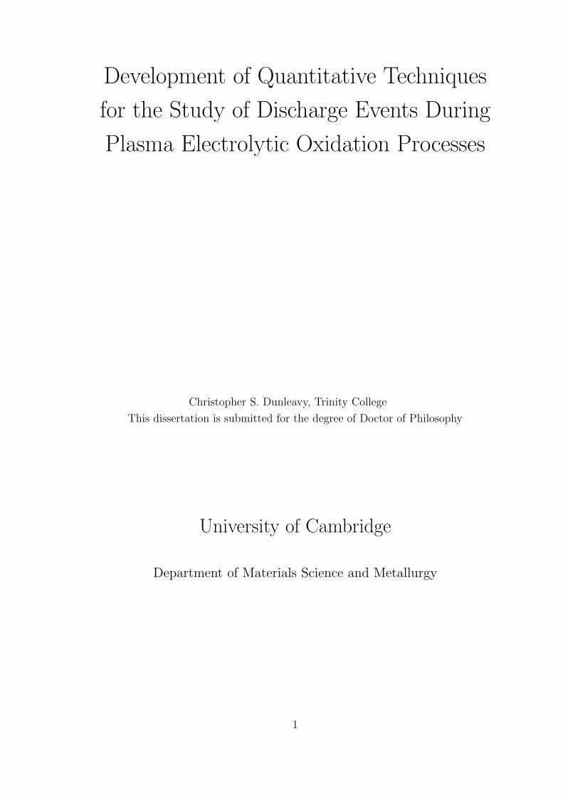
reproduced in Figure 2.1. The events had durations of ∼ 200 µs and were separated
by a period of ∼ 350 µs.
A record of a similar event, but much shorter at ∼ 1 µs duration, was presented
in more recent work by Kasalica et al [10]. This work related to the end stages of
more conventional anodising of an aluminium substrate, and as such the discharge
event captured is probably a good representation of the initial discharges during
PEO processing.
Application of high speed video imaging in the range of 5400 to 20 000 frames
per second was reported by Arrabal et al for PEO processing of pure magnesium and
22
Figure 2.1: Traces of single spark reaction on tip of stainless steel needle. Figure
and caption reproduced from Bao Van et al [13]
a range of magnesium alloys [5]. In this optical study lifetimes of the shortest lived
discharges were found to be in the range ≤ 50− 185 µs, and the average lifetime
was estimated as 500− 1100 µs.
Discharge lifetimes in the range of ∼ 10 − 100 µs were reported in work by
Dunleavy et al [1], which applied two different methodologies. The first was low
power DC processing of pre-deposited PEO coatings on aluminium. The second
involved monitoring the current through a small aluminium area (500 µm diameter)
which was processed in parallel with a larger area under more standard coating
growth conditions.
Several sources quote discharge duration values from papers published in Rus-
sian. Typical durations in the range 100− 500 µs are quoted by Terleeva et al [18],
with reference to a book published by Bakovets et al [19]. It is not clear whether
this value was derived from electrical monitoring or high speed image capture. It is
also not stated which substrate these values refer to, though aluminium is perhaps
the most likely given the longer history of PEO on aluminium.
A similar range of 10− 100 µs was quoted by Long et al [20] and attributed to
Snezhko and Chernenko [21]. Values of typical current from the study by Snezhko
and Chernenko are also quoted, which implies that this range was determined by
electrical monitoring. Information on the substrate metal was not provided.
23
A shorter range of 10− 20 µs was stated by Gnedenkov et al [22], with reference
to a book by Gordienko and Gnedenkov relating to processing of titanium [23].
The Gordienko and Gnedenkov value is most likely to be derived from electrical
monitoring as Gnedenkov et al also quote values for typical event currents and
power levels.
A study which applied video imaging to study discharge lifetimes by Golovanova
and Sizikov [24] was cited by Yerokhin et al [2] as having ascertained the discharge
lifetime to be ≤ 7.5 ms, the upper bound is presumably determined by the temporal
resolution obtainable from the imaging system used.
Imaging of titanium PEO processing by Matykina et al [8] used a camera system
with 10 ms exposure time and a 40 ms shutter interval. Probability distributions
of apparent discharge lifetimes were presented for three values of the applied volt-
age, each corresponding to a later time during processing. The discharge apparent
lifetimes were reported as ∼ 35− 100 ms at 300 V, ∼ 35− 260 ms at 370 V and
∼ 100− 800 ms when the applied voltage had reached 430 V.
Given the temporal resolution in this study, and considering the other values
quoted in the literature for discharge lifetimes, it is unlikely that the discharge
lifetimes quoted by Matykina et al [8] represent single discharge events. More likely
the slow sampling rate and long exposure time for each image allows a prolonged
series of much shorter discharge events, occurring at the same point on the surface,
to appear in the images as a single long-lived event. Whilst such slow (relative
to the discharge lifetime) video imaging cannot yield usable data on the discharge
durations, the results suggest increasing persistence and localisation of discharge
events as coating progresses.
An estimate of the discharge lifetime is made by Yerokhin et al [2] in an opti-
cal imaging study of aluminium PEO processing, though not from the individual
frames themselves. The video was taken at only 24 Hz, when the processing was
AC with frequency 50 Hz. The authors instead identified the apparent area under
discharge from the video stills. They then estimated the current density through
each discharge and used that to estimate the time required to raise the local volume
of coating to a temperature great enough to cause alumina to melt. They reported
values in the range 0.25− 3.5 ms.
The literature data on discharge event durations is summarised in Table 2.1.
With the exception of studies which used inappropriate measurement time-scales,
the consensus appears to be discharge event lifetimes of the order tens to hundreds
of µs.
24

Substrate Technique Duration / µs Source
nickel plated steel electrical ∼ 200 [13]
aluminium electrical ∼ 1 [10]
magnesium optical 50− 1100 [5]
aluminium electrical 10− 100 [1]
100− 500 [19]
electrical 10− 100 [21]
titanium electrical 10− 20 [23]
≤ 7500 [24]
titanium optical 35 000− 800 000 [8]
aluminium theoretical 250− 3500 [2]
Table 2.1: Summary of the discharge duration data from literature sources.
2.1.3 Discharge event currents.
The discharges visible in Figure 2.1 from Bao Van et al [13] reach peak currents of
52 mA and 70 mA. The corresponding peak power reached by the 70 mA discharge
is quoted to be 35 W, given the applied voltage of 500 V. The calculated energy
transferred by this event was quoted as 2.9 mJ. By assuming that the area of the
discharge was identical to that of the exposed nickel plated needle, 17.8 µm in diame-
ter, they estimated discharge current densities for the two events of 2.1× 10⁸ A.m−2
and 2.83× 10⁸ A.m−2.
The discharge event plotted in an article by Kasalica et al [10] is reproduced
in Figure 2.2. The peak current reached by the discharge event is ∼ 1 mA. The
average energy quoted for the discharge events was ∼ 0.2 µJ. Based on analysis of
the observed pores in the coating exterior surface, the authors estimate a discharge
current density of ∼ 109 A.m−2.
The current density of discharge events reported by Yerokhin et al [2] varied with
duration of processing. Starting from ∼ 5× 10⁴ A.m−2 one minute into processing,
the current density, calculated from analysis of video stills at 24 Hz, was seen to
drop to ∼ 2× 10⁴ A.m−2 after 80 minutes of processing.
The individual discharge current quoted by Terleeva et al [18] is 100 mA, cited
from Bugaenko et al [25] and Polyakov and Bakovets [19]. Also cited by Terleeva et
al are values of the current density in discharge events. Values of 3× 10⁸ A.m−2 and
1× 10⁷ A.m−2 were referenced to Snezhko [26]. A separate value of 2× 10⁸ A.m−2
was attributed to Markov and Mironova [27]. Discharge current densities reported
by Terleeva et al [18] for three experimental systems are in order of magnitude
agreement at 0.2− 2× 10⁸ A.m−2. These were estimated from the total sample
25
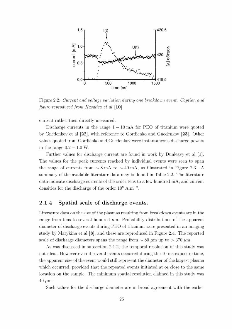
Figure 2.2: Current and voltage variation during one breakdown event. Caption and
figure reproduced from Kasalica et al [10]
current rather then directly measured.
Discharge currents in the range 1− 10 mA for PEO of titanium were quoted
by Gnedenkov et al [22], with reference to Gordienko and Gnedenkov [23]. Other
values quoted from Gordienko and Gnedenkov were instantaneous discharge powers
in the range 0.2− 1.0 W.
Further values for discharge current are found in work by Dunleavy et al [1].
The values for the peak currents reached by individual events were seen to span
the range of currents from ∼ 8 mA to ∼ 40 mA, as illustrated in Figure 2.3. A
summary of the available literature data may be found in Table 2.2. The literature
data indicate discharge currents of the order tens to a few hundred mA, and current
densities for the discharge of the order 108 A.m−2.
2.1.4 Spatial scale of discharge events.
Literature data on the size of the plasmas resulting from breakdown events are in the
range from tens to several hundred µm. Probability distributions of the apparent
diameter of discharge events during PEO of titanium were presented in an imaging
study by Matykina et al [8], and these are reproduced in Figure 2.4. The reported
scale of discharge diameters spans the range from ∼ 80 µm up to > 370 µm.
As was discussed in subsection 2.1.2, the temporal resolution of this study was
not ideal. However even if several events occurred during the 10 ms exposure time,
the apparent size of the event would still represent the diameter of the largest plasma
which occurred, provided that the repeated events initiated at or close to the same
location on the sample. The minimum spatial resolution claimed in this study was
40 µm.
Such values for the discharge diameter are in broad agreement with the earlier
26
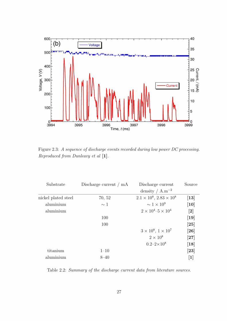
Figure 2.3: A sequence of discharge events recorded during low power DC processing.
Reproduced from Dunleavy et al [1].
Substrate Discharge current / mA Discharge current Source
density / A.m−2
nickel plated steel 70, 52 2.1× 10⁸, 2.83× 10⁸ [13]
aluminium ∼ 1 ∼ 1× 10⁹ [10]
aluminium 2× 10⁴–5× 10⁴ [2]
100 [19]
100 [25]
3× 10⁸, 1× 10⁷ [26]
2× 10⁸ [27]
0.2–2×10⁸ [18]
titanium 1–10 [23]
aluminium 8–40 [1]
Table 2.2: Summary of the discharge current data from literature sources.
27

Figure 2.4: Microdischarge characteristics during PEO treatment of titanium at
20 mA.cm−2 in 0.026 M Na3PO4: (b) microdischarge diameter. Caption and figure
reproduced from Matykina et al [8].
video imaging studies by Yerokhin et al [2, 7]. In these works the most common
events at all times of processing were found to have a mean diameter of ∼ 160 µm.
These were termed ‘small’ by the authors. It should be noted that the authors
reported the apparent cross sectional areas of events, I have assumed circular sym-
metry to estimate diameters. Also studied were ‘medium’, ‘large’ and ‘very large’
breakdown events, with average apparent diameters of ∼ 340 µm, ∼ 540 µm and
∼ 1000 µm respectively.
Results of both studies by Yerokhin et al are summarised in Table 2.3. The much
larger apparent sizes of some events recorded in these two studies, compared to the
Matykina et al study, could be due to a number of factors. The camera capture
rate of 24 Hz is slower than the 10 ms exposure time in the work by Matykina
et al. Secondly the processing was continued for a longer period of time, and the
largest events only became significant after 35 minutes of coating deposition. In
addition the substrate metal studied by Yerokhin and co-workers was aluminium,
not titanium, which is potentially significant. The most prevalent events, with
average apparent diameters of 160 µm and 340 µm, are in good agreement with the
results obtained by Matykina et al.
28

Time / min ‘small’ ‘medium’ ‘large’ ‘very large’
1 0.96 0.04 0 0
15 0.8 0.18 0.01 0.01
25 0.73 0.23 0.02 0.02
35 0.67 0.27 0.02 0.04
65 0.77 0.11 0.08 0.04
Table 2.3: Fractional distributions of discharge populations from Yerokhin et al
[2, 7].
2.1.5 Discharge event spatial density.
The number of discharge events active at any given time can be estimated from
optical imaging studies of PEO processing. Comparison between studies is possible
if the quoted density of discharges per unit area is divided by the camera exposure
time used, yielding a rate of discharging per unit area.
Matykina et al [8] report discharge densities of ∼ 5× 10⁶ m−2.s−1 after about
160 s, rising to to ∼ 2× 10⁷ m−2.s−1 after 900 s of processing. The maximum
population density seen was ∼ 3× 10⁷ m−2.s−1 around 760 s into processing. These
results were for a frame exposure time of 10 ms and DC processing of titanium.
Yerokhin et al [2, 7] report comparable values, though showing a different trend.
They found discharge densities of ∼ 6× 10⁷ m−2.s−1 around 10 minutes into pro-
cessing, falling gradually to ∼ 2.6× 10⁷ m−2.s−1 after 60 minutes. This work related
to processing of aluminium and used a frame rate of 24 Hz, corresponding to a frame
time of 41.7 ms.
An indication of the effect of current density on the breakdown event frequency
is provided by the study of Moon and Jeong [9]. Current densities of 5 and
10 A.dm−2 were applied in PEO processing of aluminium. The exposure time used
was 30 ms. For processing with 5 A.dm−2 the discharge density was found to be
∼ 1.7× 10⁷ m−2.s−1 after about 30 s, falling off to ∼ 3.3× 10⁶ m−2.s−1 after 300 s.
Greater initial discharge densities were seen for processing using a current den-
sity of 10 A.dm−2, with ∼ 5× 10⁷ m−2.s−1 after 60 s, falling to ∼ 3.3× 10⁶ m−2.s−1
after 300 s. Such values are consistent with Matykina et al [8] and Yerokhin et al
[2, 7].
The high speed optical studies by Arrabal et al [5] utilised a frame rate of
5400 frames per second to study the processing of pure magnesium and several
alloys. The exposure time of 185 µs makes this one of the most reliable information
sources, however the discharge densities reported are significantly greater than the
other optical studies. Instantaneous discharge rates spanning the range 108 m−2.s−1
29

to 109 m−2.s−1 are reported.
The discrepancy could be due to the exposure time being shorter in the work of
Arrabal et al [5]. If many discharge events occur close to a single location in rapid
succession, then with an exposure time of many ms these will appear as a single
event, reducing the apparent discharging rate. The difference of ∼ 102 in apparent
rate between the results of Arrabal et al and the other optical studies is probably
related to the similar ∼ 102 difference in frame rate, and the fact that the exposure
time of 185 µs is similar to both the discharge event lifetime and the separation
between discharge events (see subsection 2.1.2). The value obtained by Arrabal et
al is likely the most accurate reflection of discharge event rate. Comparison to the
slower optical studies is suggestive that clustering of events around specific active
locations is likely.
2.1.6 Discharge plasma composition.
Based on indexing of emission lines, the plasma composition is found to be domi-
nated by atomic and singly ionised species [1, 5, 10, 14, 15, 17]. Molecular OH
has also been reported by some studies [1, 5, 15, 17]. Doubly ionised Al has been
reported by Klapkiv et al [14]. In addition to O, H and the substrate material,
signatures of alloying elements in the substrate, and elements incorporated from
the electrolyte are also observed. These results support a view that the discharge
events provide a mass transport pathway through the coatings as they grow, because
optical emissions are observed from elements only present in the substrate.
2.1.7 Discharge plasma temperature.
Several studies have applied optical spectroscopy to estimate the plasma electron
temperature. Klapkiv et al used the relative intensity of atomic and ionic emission
lines to estimate temperatures in the range 3500 to 12 000 K [14]. The wide spread
was attributed by the authors to the existence of a hot core and cooler periphery
region in the discharge plasma.
Such results are supported by several independent measures in an article by
Dunleavy, Golosnoy et al [1]. Temperatures of ∼ 3500 K were derived from the
intensity ratio of the Balmer Hα (656.3 nm) and Hβ (486.1 nm) emission lines; anal-
ysis of intensity of the recombination continuum and from the relative intensities
of the OH molecular rotation lines. Temperatures of ∼ 16 000± 3500 K were esti-
mated from emission lines of singly ionised magnesium (which originated from the
substrate alloy), and confirmed by examination of singly ionised silicon ions.
Further confirmation of these temperature ranges was provided in a more ex-
30

tended spectroscopic study by Hussein et al [15]. This work monitored specific
spectral lines over 60 minutes of PEO processing. Temperatures ranging from 4500
to 10 000 K were reported based on intensity ratios of emission lines from atomic
aluminium species.
Electron temperatures in the range from 3000 to 16 000 K are reported for the
plasmas associated with PEO discharges. Whether the high and low temperatures
calculated from different portions of the spectrum correspond to a hot core and
cooler periphery of each event; to a hot initial stage which expands and cools, or to
entirely seperate events, is not possible to say at present.
2.2 Bulk electrical properties of PEO processing.
Bulk current and voltage waveforms for PEO processing, and properties such as
the peak current and voltage during each process cycle, are important parameters
from a quality control perspective. An example of both the process waveforms at
one time, and the behaviour of maximum and minimum current and voltage with
time of processing is reproduced in Figure 2.5 from work relating to aluminium by
Yerokhin et al [2]. An additional example was given in the introductory chapter in
Figure 1.1.
In the article from which Figure 2.5 is reproduced, the coating thickness is
reported to increase between 20 and 80 minutes from 18.9± 3.4 to 80.4± 5.0 µm,
an increase of a factor of approximately 4 times. The voltage did not undergo
an increase in proportion with the thickness. One interpretation of this is that
the applied voltage is primarily developed over a relatively thin internal region of
the coating. This idea will be discussed further in relation to coating porosity
(subsection 2.3.4) and internal structure (subsection 2.3.3).
The behaviour of bulk current and voltage shown in Figure 2.5 and Figure 1.1
is typical for PEO processing, showing a rapid initial rise of the voltage, which
after a short time slows to a reduced rate of increase for the rest of processing.
There are examples in the literature of different behaviours of current and voltage
characteristics, for instance Arrabal et al report a substantial (100–150 V) decrease
in magnitude of the applied voltage for processing of magnesium alloys beyond 400 s
[5].
31
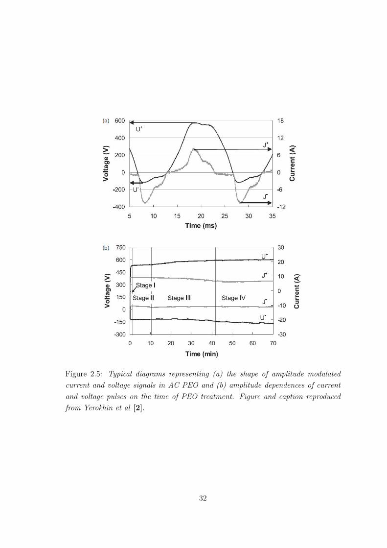
Figure 2.5: Typical diagrams representing (a) the shape of amplitude modulated
current and voltage signals in AC PEO and (b) amplitude dependences of current
and voltage pulses on the time of PEO treatment. Figure and caption reproduced
from Yerokhin et al [2].
32

2.3 Structural features of PEO coatings.
2.3.1 Growth rates and thicknesses of PEO coatings.
An attractive feature of the PEO process is that reasonably high, and often lin-
ear, growth rates can be sustained until thicknesses up to several hundred µm are
reached. Growth rates and processing conditions for articles which reported lin-
ear growth of PEO coatings are summarised in Table 2.4. Though conditions vary
widely, in general the growth rates range from several hundred nm to a few µm per
minute of PEO processing.
The data in Table 2.4 comes from processing using DC or low frequency (50–
100 Hz) current sources. The maintenance of such growth rates when the existing
coating is tens of µm thick has informed the generally held view that the discharge
events provide pathways for mass transport through the growing oxide coatings.
More direct evidence of this from the literature is discussed in subsection 2.3.6.
Not all studies have reported constant growth rates for PEO coatings, though
in many cases the thickening rate is linear for some initial period of the processing
[17, 20, 32, 33]. In these studies the growth rates were of the same order of
magnitude as those reported in Table 2.4, but changed noticeably at some point
during processing. As yet no consistent trends emerge from the studies which report
non-linear coating growth, and the underlying causes of such variations are not
known.
The important information from literature growth rates is that deposition of
PEO coatings can proceed at rates from several hundred to a few thousand nm
per minute, until coatings are over 100 µm in total thickness. At the same time
the voltage applied does not increase in proportion to the coating thickness (sec-
tion 2.2). The implications of this will be discussed further in subsection 2.3.3 and
subsection 2.3.4.
2.3.2 Exterior surfaces of PEO coatings.
SEM imaging of coating free surfaces is amongst the most common characterisation
techniques applied, and the majority of articles written about PEO include one
or more SEM images of the coating exterior. This has been a productive source
of indirect information about conditions during processing, with inferences being
made from observation of surface features. For example there are always pores, or
craters, on the surface, and these are usually associated with the discharge events.
33

Electrolyte Substrate j time rate source
/g.l−1 /A.m−2 /min /µm.min−1
alkali silicate Al 7075 3000 30 1.45 [3]
1–2 KOH &
3–5 Na2SiO3 & Al 6082 1000 100 1.00 [4]
3–5 Na4P2O7
2.8 KOH & 99.99% Al 500 90 0.57 [28]
5.3 Na2SiO3
KOH & Al 2214-T6 3800 200 0.80 [16]
Na2SiO3
KOH & Al 6082 1500 150 0.67 [29]
Na2SiO3 2700 150 1.17
NaWO3 & Al LD31 800 180 0.36 [30]
Na3PO4
2.8 KOH &
5.3 Na2SiO3 99.99% Mg 2000 40 0.95 [31]
with 10 ZrO2 40 1.10
2.8 KOH & Mg WE43-T1 3000 40 0.43 [32]
5.3 Na2SiO3
9.5 Na3PO4 & Mg WE43-T1 3000 40 0.70 [32]
52.5 NH4OH
Table 2.4: Summary of linear coating growth behaviours for PEO processing which
have been reported in the literature, j is the applied current density.
34

2.3.2.1 Appearance of coating surfaces.
PEO coatings on aluminium display a characteristic surface appearance, of which
the micrographs reproduced in Figure 2.6 are a typical example. The coatings at
all times exhibit pores (craters) on scales from a few hundred nm up to a few µm.
These pores are often surrounded by relatively smooth regions of material, which
are speculated to be formed from the re-solidification of molten material after a
discharge event.
Cracks radiating from the craters have been attributed to thermal shock caused
by rapid quenching [4]. Evidence of melt flow and solidification would suggest that
temperatures in the region of the discharge reach several thousand Kelvin. This is
consistent with the plasma temperature estimates from spectral studies [1, 14, 15].
The increasing scale of surface features with processing time is usually attributed
to increased intensity and power of discharge events as coating proceeds.
2.3.2.2 Discharge channel sizes and populations.
Sundararajan and Rama Krishna [3], and Shen et al [34] studied variation in the
diameters of open pores (craters) with processing time. Both studies found an ap-
proximately linear increase in channel diameter with processing time. Sundararajan
and Rama Krishna found the diameter to vary from ∼ 1.4 µm after 1 minute, to
∼ 2.4 µm after 30 minutes of processing. This related to the 5 largest pores observed
in each micrograph. This represents an upper bound on discharge channel scale,
as smaller pores were still present. The trend found in this study is reproduced in
Figure 2.7.
Shen et al [34] found the diameter to increase from ∼ 1 µm after 1 minute
to ∼ 9 µm after 36 minutes of processing. This is a much larger increase than
reported by Sundararajan and Rama Krishna [3]. However it is not clear from the
methodology of De-Jiu et al exactly which channel diameters they have included,
and no errors are estimated for their channel diameter measures. It is unlikely the
numbers plotted represent a mean, as micrographs in the same article indicate that
much smaller pores are present for all times of processing.
Estimates of the number of discharge channels per unit area have also been pub-
lished. For aluminium processing Sundararajan and Rama Krishna report a density
of ∼ 1.1× 10¹⁶ m−2 after 1 minute, falling with processing time to ∼ 5× 10¹⁴ m−2
after 30 minutes [3]. Studies of PEO on aluminium were also published by Shen
et al [34] and Curran and Clyne [4]. Shen and co-workers report lower discharge
channel populations, of ∼ 3.8× 10¹¹ m−2 at 1 minute, falling to ∼ 1× 10¹⁰ m−2
after 36 minutes.
Curran and Clyne [4] found a population density of ∼ 1.4× 10¹⁰ m−2 for a
35

Figure 2.6: Secondary electron images of MAO coating surfaces at 500× magnifi-
cation processed for (a) 1; (b) 3; (c) 5; (d) 10; (e) 20 and (f) 30 min. Figure and
caption reproduced from Sundararajan and Rama Krishna [3], substrate material
was aluminium.
36

Figure 2.7: Variation in diameter of the microarc discharge channels as a function
of MAO processing time. Figure and caption reproduced from Sundararajan and
Rama Krishna [3].
5 µm coating (approximately 5 minutes processing), falling to ∼ 1× 10⁹ m−2 when
a coating thickness of 40 µm had been reached. Thereafter the crater population
density remained approximately level to a thickness of 100 µm (about 100 minutes
processing). For PEO processing of titanium, Matykina et al found pore popula-
tion of ∼ 3.5× 10¹¹ m−2 2 minutes into processing, which was observed to fall to
∼ 1× 10¹¹ m−2 after 15 minutes [8].
With the exception of Sundararajan and Rama Krishna, the literature data
indicates the pore population density to be in the range from 109 to 1011 m−2.
The information about visible crater (pore) populations, when combined with esti-
mates of dynamic discharging rates, can enable estimates to be made of the period
for which surface features persist before being overlaid by subsequent discharging
activity. For example with a discharging rate of 1× 10⁸ m−2.s−1 and a crater popu-
lation of 1× 10¹⁰ m−2, you would expect the lifetime of a particular surface feature
to be roughly 100 s. All studies reported significant decreases in the number of
pores visible on the coating exterior with increased thickness.
2.3.2.3 Surface roughness of coatings.
Increases in exterior roughness of PEO coatings with processing time are well known,
and evident upon examination at the human scale by eye and touch. Some authors
37
have quantified these changes in surface roughness, which are thought to provide
an indirect measure of the scale and uniformity of discharging activity.
The characterisation study by Sundararajan and Rama Krishna included quan-
tification of the coating roughness [3]. They report a linear increase in the coating
arithmetic roughness from ∼ 0.3 µm just after commencement of processing, to
∼ 2.2 µm when the coatings were about 40 µm thick after 36 minutes processing.
The authors also quantified the typical diameter of the smooth regions of ap-
parently re-solidified material surrounding discharge craters, finding ∼ 15 µm at 5
minutes into processing, then a rough linear increase to ∼ 35 µm after 30 minutes.
They speculate that growth of the coating is by flow of molten material out of the
discharge channel, which spreads to form the smooth regions which they refer to as
‘pancakes’. The authors speculate that increases in the mean ‘pancake’ diameter,
when coupled with the decrease in crater population density, may be the cause of
the increased roughness seen with thickening of the coatings.
Comparison can be made with the study by Curran and Clyne [4], who reported
arithmetic roughness ∼ 1.5 µm for a 5 µm coating, which increased until levelling
off at ∼ 8 µm from 80 µm to 100 µm of coating thickness. Jin et al reported a linear
increase in the observed arithmetic roughness of PEO coatings [30]. They found
an increase from ∼ 1.3 µm for 15 µm coatings to ∼ 4.5 µm when the coating was
more then 65 µm in thickness. Data from Curran and Clyne [4] and Jin et al [30]
are in reasonable agreement with Sundararajan and Rama Krishna [3].
The ‘pancake’ concept of Sundararajan and Rama Krishna was adopted by
Jaspard-Mecuson et al [16], they reported initial diameters for the smooth sur-
face regions of ∼ 15 µm after 10 minutes processing. This then rose in roughly
linear fashion to ∼ 110 µm after 140 minutes of conventional PEO processing. The
implied value of ∼ 30 µm after 35 minutes processing compares reasonably with
the values reported by Sundararajan and Rama Krishna [3]. They also report on
an experimental set of processing conditions which they state displayed reduced
intensity of discharging when observed visually. For this experimental process they
found the ‘pancake’ diameter to be roughly constant at around 20 µm throughout.
The trends in surface roughness are related to increases in the scale of surface fea-
tures as PEO coatings thicken. In the context of information on size and prevalence
of discharge channels (subsubsection 2.3.2.2), and if feature size is assumed propor-
tional to some energy input from processing, the literature data suggests greater
local intensity of processing at a reduced number of sites as coating proceeds.
38

2.3.3 Coating interior microstructures.
PEO coatings are often reported to show a two layer structure, with an outer layer
described variously as porous or friable, and an inner layer described as dense,
compact or functional. Such a structure has been reported for Aluminium by Guan
et al [35], Jaspard-Mecuson et al [16], Gu et al [36], Long et al [20], Yerokhin et
al [2, 33] and Xue et al [37]. For magnesium processing, two layer structures are
reported by Arrabal et al [5, 31, 32]. In relation to titanium, a two layer structure
was reported by Teh et al [38].
There are certainly differences in the coating morphology through the cross
section, as seen in Figure 2.8, reproduced from [4]. However, there is no clear
boundary between two regions of coating, what change there is happens gradually
between the substrate and the free surface. Claims of obvious two layer structures
in the literature are sometimes tenuous, and the relative thickness of ‘porous’ and
‘functional’ layers is often used as a parameter to quantify the relative quality
of different processing conditions. Using a subjective measure like this for such
purposes is not ideal.
Some studies have used TEM imaging to focus on the boundary between the
coating and substrate. This interface is important for coating corrosion performance
and adhesion to the substrate. A thin, typically several hundred nm thickness,
barrier layer of amorphous material has been reported at the substrate-coating
interface for aluminium by Monfort et al [28], for titanium by Matykina et al [39]
and for magnesium by Arrabal et al [5].
The interpretation of these authors is that much of the coating thickness is
permeable to the electrolyte via a network of surface connected porosity, and that
only this internal region presents a barrier to electrical conduction and corrosion of
the substrate. This is a reasonable conjecture, especially as the voltage required to
cause breakdowns through a coating during PEO does not double with the coating
thickness (see section 2.2). It makes sense that the majority of the applied voltage
be dropped over some thinner internal region of the coating, with discharge events
possibly initiated at this internal barrier. This is consistent with the observation
that PEO coating rates can remain reasonably constant to thicknesses in excess
of 100 µm. The conjecture that the majority of the coating be permeable to the
electrolyte relies upon a high level of surface connected porosity in the coating,
which will be discussed in subsection 2.3.4.
39

Figure 2.8: Back-scattered SEM micrograph of a polished cross-section through a
100 µm thick coating, showing surface cracks, shrinkage pipes and an extensive
network of micro-defects. Figure and caption reproduced from Curran and Clyne
[4].
40

Technique Porosity
free standing bulk density 42± 12%
attached bulk density 50± 14%
mercury porosimetry 17± 7%
nitrogen adsorption 20%?
Table 2.5: Summary of the porosity measurements reported by Curran and Clyne
[6]. ? this value is an estimate assuming cylindrical pores of 30 nm diameter, as
nitrogen adsorption measures specific surface area.
2.3.4 Coating porosity.
Dietzel et al studied porosity of coatings on magnesium indirectly by examination of
coating surfaces after either chemical etching or electro-deposition of copper, which
was preferentially deposited at sites of pores in the coating surface [40]. They quote
pore numbers in the range of ∼ 5× 10⁶ m−2 to ∼ 6× 10⁷ m−2, though no fraction
of porosity is quoted. The pore density identified is much lower than that quoted
by other studies.
An estimate of the porosity as less than 10% was reported by Yerokhin et al
from analysis of polished cross-sections [33]. This estimate is probably too low as
polished cross-sections do not represent the most reliable approach to measurement
of porosity. Much of the porosity may not show up clearly, and the polishing process
can result in sample porosity being filled in with material dislodged from elsewhere
on the sample surface.
The most expansive study of porosity was published by Curran and Clyne [6].
They estimated the porosity for coatings on aluminium by measurement of the bulk
density of both attached PEO coatings and coatings detached by dissolution of the
substrate. Porosity was also measured using mercury intrusion porosimetry and
isothermal nitrogen adsorption. A summary of the measured porosity values may
be found in Table 2.5.
The fraction of surface connected porosity was estimated by comparison of the
skeletal density, as measured by Archimedian displacement, He pycnometry or mer-
cury porosimetry, with the theoretical skeletal density from the phase proportions
measured by X-ray analysis. A summary of the skeletal densities reported by the
authors is found in Table 2.6.
Porosity values from bulk density measurements are probably the least reliable.
The coating dimension was measured for free standing coatings with a micrometer,
and for attached coatings by eddy current thickness gauge. These techniques are
not sensitive to the surface roughness of the coatings, and will tend to measure the
41

Technique Skeletal Density / g.cm−1
theoretical 3.63± 0.2
Archimedian 3.73± 0.02
He pycnometry 3.498± 0.004
mercury porosimetry 3.609± 0.004
Table 2.6: Summary of the skeletal density measurements reported by Curran and
Clyne [6].
thickest points on the area tested. This will lead to an overestimate of the thickness
and porosity. The values from mercury porosimetry, and estimated from nitrogen
adsorption, around 20%, are probably the most accurate reflection of the coating
porosity.
The similarity reported between the theoretical skeletal density from X-ray anal-
ysis and the three different experimental measurements is evidence of low levels of
occluded porosity in PEO coatings. This implies that the majority of porosity in
PEO coatings is connected to the coating surface. This would allow for infiltration
of the electrolyte into the bulk of the coating during processing, and is consistent
with the conjecture in subsection 2.3.3.
2.3.5 Phase constitution.
The crystalline phases, and the relative fractions of each present, are thought to be
influenced by the heating effects of the plasma discharges during processing. For
aluminium the most common constituents have been often confirmed to be α and
γ-alumina [2, 3, 4, 28, 29, 30, 33, 35, 36, 37, 41, 42, 43]. Other polymorphs
of alumina, such as δ and θ-alumina, were detected in some of these studies, and
aluminosilicate phases such as mullite were detected in some of the studies which
utilised electrolytes with a high concentration of Na2SiO3.
Crystalline phases detected in PEO coatings on magnesium included MgO,
Mg2SiO4, MgSiO3 and Mg3 (PO4) [5, 32]. For titanium the main phases iden-
tified are anatase and rutile forms of TiO2 [44]. Anatase and rutile were also seen
in selected area electron diffraction analysis by Matykina et al [39]. Other works
in addition have no doubt found similar phases to those mentioned, the papers
referenced in this work correspond to studies where some emphasis was placed on
process mechanisms, and not tribological or biomaterials applications.
The α-alumina structure is the stable form of Al2O3 [45]. There are a number of
structurally similar transition alumina polymorphs, and these may co-exist within
a single sample at a given temperature and pressure [45, 46, 47, 48]. This makes
42

single crystal samples of transition aluminas difficult to achieve, and as a result the
exact structures of γ, δ and θ-alumina structures are not completely resolved. All
are based roughly around face centred cubic arrangement of the oxygen anions, with
the different symmetries being realised by differing arrangements of the Al cations.
The γ-alumina phase may be formed from thermal oxidation of aluminium; heat-
ing of aluminium hydrates; transformation of amorphous Al2O3 and from quenching
of alumina melt [45]. Most of these routes could be feasible in the PEO process.
Furthermore, γ-alumina can also be directly formed during anodising of aluminium
under certain conditions, and is associated with oxygen generation [28, 43].
Once γ-alumina has been formed, it may be transformed into α-alumina either
directly, or via intermediate transformation to δ then θ-alumina [45, 48]. The
temperature required for transformation of γ to δ is ∼ 1023 K, for δ to θ ∼ 1273 K
and above ∼ 1473 K any of the transition aluminas can undergo transformation to
the stable α form.
The existence of α-alumina in PEO coatings is indicative of local temperatures
in the coating reaching at least ∼ 1473 K. The existence of δ and θ-alumina poly-
morphs is not unfeasible given the possible transformation routes between γ and
α-alumina. Generation of α-alumina in PEO coatings is usually attributed to ther-
mal annealing effects of the discharges. Knowledge of the physical scale of events,
and of the energy and power delivered to individual plasma discharges is thus cru-
cial; if the thermal fields in PEO coatings near to a discharge event are to be
calculated to allow testing of this hypothesis.
Relative fractions of phases at different depths below the free surface of a
∼ 70 µm PEO coating were measured using X-ray spectroscopy and Rietveld re-
finement for PEO coatings on aluminium by Curran and Clyne [4]. The results are
reproduced in Figure 2.9; the content of α-alumina is seen to be highest in the outer
30–40 µm of the coating.
By contrast, Xue et al [37] found the opposite trend, with the lowest content of
the α phase at the coating surface, ∼ 12%. The proportion rose with depth below
the coating free surface to ∼ 56% when 50 µm from the interior boundary with the
substrate. In both cases the authors attribute the higher content of α-alumina to
greater thermal effects of the discharges, though there is clearly a discrepancy in
their assumptions about where in the coating system heat loss will be a minimum.
It seems unlikely that thermal effects in the two experiments would be sub-
stantially different with depth into the coating. It is possible that another factor
is responsible for the observed phase distributions, possibly the concentrations of
alloying elements. Impurities are said by Levin and Brandon [45] to have a bearing
on transition temperatures and stability of transition aluminas. Curran and Clyne
43

Figure 2.9: X-ray diffraction data in the form of a plot of the phase proportions
against the nominal depth below the free surface for surface scans during the pro-
gressive polishing of a 100 µm thick coating. Figure and caption reproduced from
Curran and Clyne [4].
44

[4] used Al 6082, Xue et al [37] used Al 2024, which contains substantially more Cu
then the 6082. Without detailed information about differences in discharge event
power levels between different processing systems, further progress in understanding
the phase proportions is difficult.
2.3.6 Elemental distributions.
The distribution of atomic elements within PEO coatings is not uniform, and often
EDX mapping of elemental compositions has been used to gain insight into the dis-
charge and coating growth mechanisms. The first work to fully realise this potential
was published by Monfort et al [43]. The authors processed aluminium sequentially
in first an electrolyte containing Na2SiO3, then a second containing (NH4)2 HPO4.
They applied EDX mapping of the coatings formed to examine the distributions of
silicon and phosphorous within the coatings.
They present maps showing that silicon was primarily present in the outer parts
of coatings when samples were processed only in the silicate containing electrolyte.
For coatings produced only in the phosphate electrolyte the phosphorous was found
predominantly in the interior regions of the coatings. Most significantly the authors
demonstrated that when a sample coated for 30 minutes in the silicate electrolyte
was processed for just 15 s in the phosphate containing electrolyte, phosphorous
could be found at some locations near to the substrate-coating boundary. A repro-
duction of these elemental maps is in Figure 2.10 for reference.
This provides valuable evidence that the PEO discharge events provide a mass
transport pathway between the electrolyte and the coating interior. Similar results
for sequential processing of magnesium alloy were reported by Arrabal et al [32],
and for titanium by Matykina et al [49]. The tendency for silicon to be found in
the coating exterior was further confirmed in studies by Monfort et al on aluminium
[28], and Arrabal et al for another study of magnesium [5].
45

substrate
resin
Figure 2.10: EPMA of the coating formed on aluminium for 1800 s at 5 A.dm−2 in
0.05 M KOH + 0.025 M Na2SiO3.10H2O electrolyte at 293 K and then for 15 s in
3 M NH4OH + 0.05 M (NH4)2HPO4 electrolyte at 293 K. a) Backscattered elec-
tron image, b) oxygen, c) silicon, and d) phosphorus. Figure and caption reproduced
from Monfort et al [43], annotations added for additional context.
46

Chapter 3
Methodology.
3.1 PEO Processing Equipment.
Two methodologies which enable quantitative information on the discharge event
properties to be measured are presented in this work. The first involves monitoring
the current passing through a small area, exposed to PEO processing in parallel with
a larger area. This approach relies upon the existence of a well defined probability
of breakdown per unit time and area. By using a small enough area, the possibility
of two or more events being active concurrently on the small area is reduced. This
allows individual breakdown events to be resolved in the current signal. This method
will be referred to as ‘in-situ monitoring’ experiments, as the data is recorded during
a full scale application of the PEO process. This work was inspired by the work of
Bao Van et al [13].
The second methodology takes a different approach to reduce the probability
of concurrent discharge events. Testing is performed on coatings pre-deposited by
conventional 50 Hz PEO processing. Small test wells are created on the sample
surface, then filled with a sample of an electrolyte to be tested with the coating.
The substrate metal is raised to a high positive voltage, as during PEO processing,
whilst the electrolyte is held at ground potential. Breakdown events are initiated
when the potential difference becomes large enough. The incidence of concurrent
events is reduced by using power supplies which are not capable of supplying large
currents for continuous periods. The current loading causes the applied voltage
to drop once an event has initiated, reducing the probability of a second event
initiating until after the first has terminated, and the applied voltage recovered.
Capacitors placed in parallel with the sample under test can provide an additional
store of charge and energy, reducing the magnitude of the drop in applied voltage
during a discharge event.
These experiments will be referred to in this text as ‘single discharge’ experi-
47

chilled water in chilled water out
Pump
power unitcontrols
50 Hz2-phase
variable capacitorbanks
safetyinterlocks
electrolyte
copper bar
sample
counter-electrode
1 Ω
100
kΩ10
MΩ
currentmonitor
voltagemonitor
whistlepump
Figure 3.1: Schematic of the 10 kW 50 Hz AC PEO processing unit used in this
research.
48

Figure 3.2: Photograph of the 10 kW 50 Hz AC PEO processing unit used in this
research.
ments. This is not always accurate, as for some experiments a significant population
of the discharge events recorded appear to be the superposition of two separate cur-
rent peaks. The name is used here in preference to the terminology of ‘small area
DC testing’, which was used in a previous publication [1]. This is because it would
be confusing to refer to these experiments as small area, when the monitored area
is several orders of magnitude larger then that used for the in-situ experiments.
The same PEO processing unit was used for both in-situ monitoring experiments
and to generate samples used for single discharge testing. The supply is depicted
schematically in Figure 3.1, and a photograph is presented in Figure 3.2. The power
unit is a 50 Hz fixed frequency unit operated from 2-phase UK mains supply. Banks
of capacitors can be switched in and out of series with the process tank, in steps
49

of 2 µF. The capacitors limit the charge which can be supplied during each 50 Hz
cycle, and in addition enforce balance of the charges supplied during positive and
negative polarisation of the sample. In standard operation the electrolyte is kept
at ground potential, and the sample is connected to the power supply output.
It should be noted that no bias of the voltage is applied directly by the power
unit. Greater voltages are generally reached under positive polarity, however this
is due to the interaction of the substrate-coating-electrolyte system with the power
supply. Application of the power supply to substrates which are inert to PEO
processing, for example stainless steel, results in symmetric voltage waveforms. Ex-
amples of the process current and voltage waveforms from this unit may be found
in Figure 1.1.
The electrolyte used for all processing and testing was a commercial electrolyte
of approximate composition 1–2 g.l−1 potassium hydroxide (KOH), 3–5 g.l−1 sodium
silicate (Na2SiO3) and 3–5 g.l−1 tetra-sodium pyrophosphate (Na4P2O7). The elec-
trolyte used had conductivity of σ = 5.1± 0.1 mS and pH of 10.9± 0.1.
The electrolyte was pumped through a heat exchanger to prevent large temper-
ature rises during processing, and passed back into the tank through an aerating
pump. The cooling water passed through the heat exchanger varied in temperature
from ∼ 16C to ∼ 18C. Electrolyte temperature was logged along with other ex-
perimental parameters. Temperature was measured by a sensor in the processing
tank, connected to a readout on the supply control unit.
The coatings produced by this 50 Hz PEO processing unit have been well char-
acterised previously [4, 6]. The processing frequency is fixed at 50 Hz, and all that
can be set on the unit are the time of processing and the capacitance, which as
previously mentioned influences the current density. It should be stressed that the
capacitance setting does not actually control the current density to a precise level.
Some modifications to the basic unit were made to allow direct logging by os-
cilloscope of the bulk current through the process tank and the voltage between
the output and ground. A 1 Ω resistor was included in the return path to ground,
allowing the current to be monitored via the voltage developed over the resistor.
The voltage was monitored by a 100× attenuation potential divider built in between
ground and the power supply output. When bulk waveforms were being logged, the
monitoring box was connected to a Picoscope 5203 PC USB oscilloscope, controlled
using a laptop computer.
50

3.2 In-situ Discharge Monitoring Experiments.
The general geometry of the samples used for in-situ current monitoring is shown
schematically in Figure 3.3. The sample consists of a cylinder of aluminium 6082
alloy with diameter of 10 mm, with one or more fine wires of 99.5% purity aluminium
running parallel. The assemblage of large and small areas was mounted in a cold
setting acrylic resin (Epofix), to provide electrical insulation from the electrolyte.
Electrical connection of the large area was through a 4 mm threaded stainless steel
rod, connected to the power supply output (Figure 3.1) by a brass clamp. Full
details of the relative scale of small and large areas of the in-situ samples can be
found in subsection 3.2.1. The small and large areas are connected via an extended
pair of wires, twisted together to reduce noise in the current signal. The twisted
pair extended out of the processing tank and was passed through a non-contact
current probe as a coil of 4 turns.
This current probe operated by electromagnetic induction, and 4 turns of the
signal wire were passed through the probe to increase the current sensitivity. The
probe used was a Tektronix P6021 current probe. The coupling into the oscilloscope
was set to a sensitivity of 1 mV per 2 mA, so with the enhancement provided by
using 4 turns of the signal wire, this gave a sensitivity of 2 mV per 1 mA. Working by
electromagnetic induction, the probe requires a changing current signal to function,
and with the settings used the low frequency cut off was 400 Hz.
The short (∼ 100 µs) current pulses which were measured in this work principally
contain frequency components greater than 400 Hz. However, the current gradient
is low, and temporarily zero, in the region of the peak discharge current. During this
period the signal in the current probe displays decay similar to a resistor-inductor
circuit (LR), leading to distortions of the measured baseline level. This phenomenon
is referred to as LR ‘droop’, and the effect may be corrected for. This correction
was made in the present work, and full details of the procedure may be found in
Appendix B.
Monitoring of the current passing through the small area was performed using
a Picoscope 5203 USB oscilloscope, controlled by a laptop computer. The voltage
between ground (electrolyte) and the sample was monitored using the built in 100×attenuation potentiometer, depicted in Figure 3.1. The oscilloscope had two data
channels, so the small area current and the bulk processing current were not recorded
in the same experiment, as one channel was reserved to monitor the applied voltage.
The sampling rate used in the in-situ experiments was 500 kHz, one sample
every 2 µs. Data was recorded in 20 s continuous sections, and after each section the
internal memory of the oscilloscope was filled. There was then a period of ∼ 2.7 s
‘dead time’ during which the oscilloscope memory was transferred to the laptop
51

currenttransformer
probe
large area
small monitored area
acrylic resin
threaded connectionto output bar
4 turns passed throughtransformer probe
Figure 3.3: Schematic of the sample geometry used for small area in-situ discharge
monitoring.
52

memory. This could not be repeated indefinitely, and periodically the processing
had to be stopped to allow the data in the laptop memory to be written to the
hard disc. As a result in-situ experiments were conducted as a sequence of 150 s
segments of PEO processing. During each processing segment, 7 oscilloscope buffers
were taken, 6 spanning 20 s and one spanning ∼ 13.8 s. The total period which was
not recorded was ∼ 16.2 s, meaning that coverage during in-situ experiments was
∼ 89.2%.
The duration of the interruption between process segments was always more then
120 s, but never more then 180 s. Interruptions to PEO processing are generally of
minimal impact once processing is resumed, however some effect of this procedure
upon the discharging behaviour might be expected. This procedure of logging,
stopping, then re-starting the processing was repeated until the desired duration
was reached. Full details of the durations of each experiment may be found in
subsection 3.2.1.
The main purpose of the in-situ experiments was to obtain information represen-
tative of bulk PEO processing. This is why a small area was monitored in parallel
with a larger area. It was desired to understand the properties of breakdown events
which occurred as part of a larger ensemble of active discharge events, spread across
the exposed substrate surface. Whilst the data obtained during any given experi-
mental run will not be representative of the wider process at that time (due to the
small area sampled), across multiple repeats the measured properties should con-
verge to a distribution which is representative of the individual discharge properties
across the whole sample at that point in time. The validity of this assumption will
be discussed in chapter 4.
The elongated shape of the in-situ samples, 120 mm in length, was chosen to
allow many repeats to be performed in rapid succession. After each experimental
run a Struers Secotom-10 precision saw was used to cut off the front 3–4 mm of the
sample. The cut off was kept for analysis by microscopy, and the newly exposed
surface ground with 800 grade SiC grit paper. The newly resurfaced sample was then
used for another experiment. The front face of the sample was always positioned
at a distance of 40 mm from the stainless steel counter electrode.
3.2.1 Variations of discharge characteristics with processing
time and effects of monitored area size.
The purpose of this experiment was firstly to measure the properties of PEO dis-
charge events during processing of an aluminium substrate, for periods up to 40
minutes of processing. Samples with several different sizes of small area were pro-
duced to confirm that rates of activity seen scaled with the size of the area moni-
53
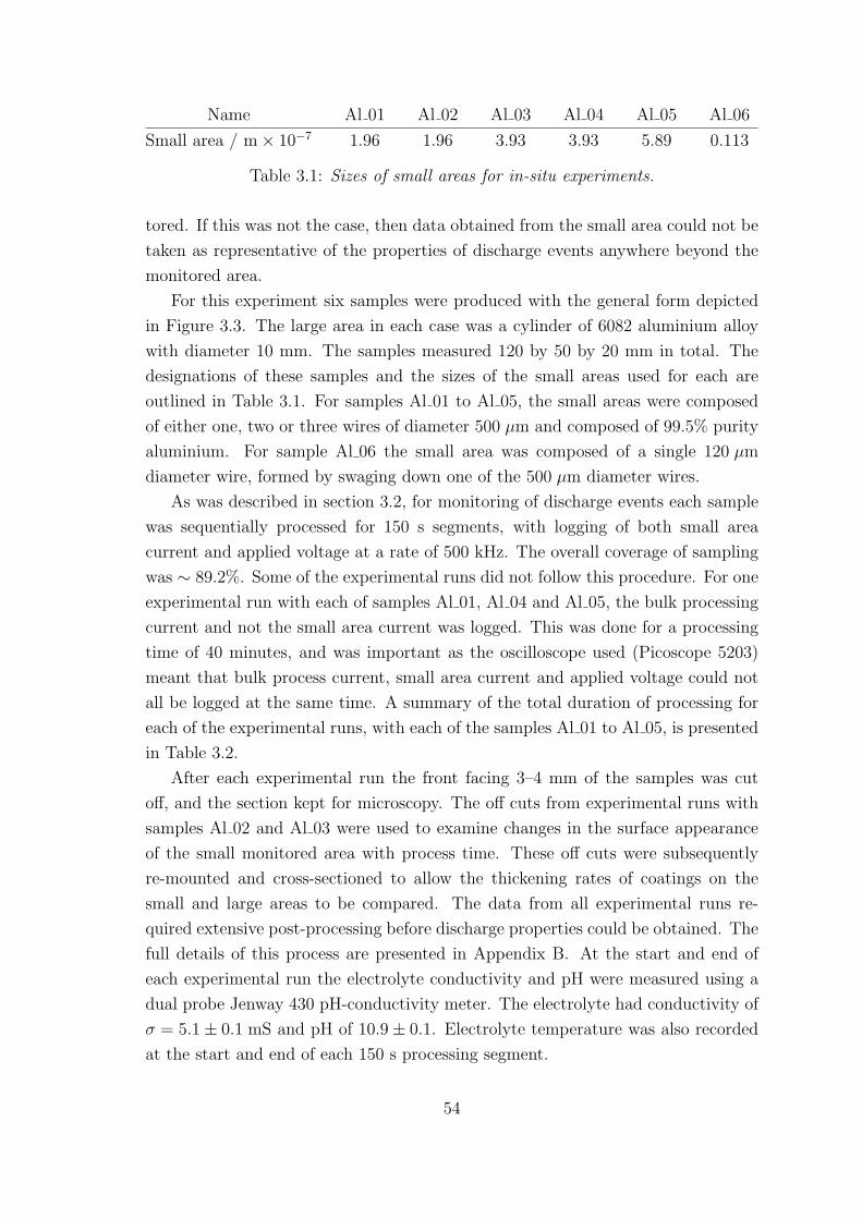
Name Al 01 Al 02 Al 03 Al 04 Al 05 Al 06
Small area / m× 10−7 1.96 1.96 3.93 3.93 5.89 0.113
Table 3.1: Sizes of small areas for in-situ experiments.
tored. If this was not the case, then data obtained from the small area could not be
taken as representative of the properties of discharge events anywhere beyond the
monitored area.
For this experiment six samples were produced with the general form depicted
in Figure 3.3. The large area in each case was a cylinder of 6082 aluminium alloy
with diameter 10 mm. The samples measured 120 by 50 by 20 mm in total. The
designations of these samples and the sizes of the small areas used for each are
outlined in Table 3.1. For samples Al 01 to Al 05, the small areas were composed
of either one, two or three wires of diameter 500 µm and composed of 99.5% purity
aluminium. For sample Al 06 the small area was composed of a single 120 µm
diameter wire, formed by swaging down one of the 500 µm diameter wires.
As was described in section 3.2, for monitoring of discharge events each sample
was sequentially processed for 150 s segments, with logging of both small area
current and applied voltage at a rate of 500 kHz. The overall coverage of sampling
was ∼ 89.2%. Some of the experimental runs did not follow this procedure. For one
experimental run with each of samples Al 01, Al 04 and Al 05, the bulk processing
current and not the small area current was logged. This was done for a processing
time of 40 minutes, and was important as the oscilloscope used (Picoscope 5203)
meant that bulk process current, small area current and applied voltage could not
all be logged at the same time. A summary of the total duration of processing for
each of the experimental runs, with each of the samples Al 01 to Al 05, is presented
in Table 3.2.
After each experimental run the front facing 3–4 mm of the samples was cut
off, and the section kept for microscopy. The off cuts from experimental runs with
samples Al 02 and Al 03 were used to examine changes in the surface appearance
of the small monitored area with process time. These off cuts were subsequently
re-mounted and cross-sectioned to allow the thickening rates of coatings on the
small and large areas to be compared. The data from all experimental runs re-
quired extensive post-processing before discharge properties could be obtained. The
full details of this process are presented in Appendix B. At the start and end of
each experimental run the electrolyte conductivity and pH were measured using a
dual probe Jenway 430 pH-conductivity meter. The electrolyte had conductivity of
σ = 5.1± 0.1 mS and pH of 10.9± 0.1. Electrolyte temperature was also recorded
at the start and end of each 150 s processing segment.
54

Experimental run Al 01 Al 02 Al 03 Al 04 Al 05
run 1 35 2.5 unusable 40 40
run 2 40 5 2.5 40 40
run 3 40 10 5 40 40
run 4 bulk log 15 10 bulk log bulk log
run 5 unusable 20 15 40 40
run 6 unusable 25 20 40 40
run 7 40 30 25 40
run 8 40 35 30
run 9 40 35
run 10 40
Table 3.2: Times of processing for in-situ samples. All times are in minutes, ‘bulk
log’ represents that the experimental run was used to log bulk process current. Several
experimental runs were rendered unusable due to technical difficulties.
The sample with the smallest monitored area, Al 06 with a single 120 µm wire
as small area, was made after the conclusion of data processing for the other five
samples. It was specifically produced to allow resolution of the very smallest dis-
charge events which occur during processing. In addition to the smaller monitored
area, the current monitoring arrangement was physically altered for this sample.
Instead of 4 turns of the signal wire being passed through the current probe, as
depicted in Figure 3.3, ten turns were used with sample Al 06. This increased the
current sensitivity of the probe to 5 mV per 1 mA. Logging with this sample was
not as comprehensive as the other samples, but was conducted at greater sampling
rates, typically 62.5 MHz.
3.3 Single Discharge Experiments.
Whilst the properties of breakdown events recorded during PEO processing are of
obvious interest, the occurrence of each event as part of a wider set of discharges
presents several problems when it is desired to understand the underlying physical
principles. For such studies the ‘single discharge’ techniques were developed.
The concept of the single discharge experiments is to generate breakdown events
as close as can be managed to one at a time. Samples used were pre-deposited PEO
coatings of varying thicknesses. Using pre-deposited coatings has several advan-
tages, the most important of which is that the electrolyte used for the testing need
not be the same electrolyte as was used to generate the coating in the first place.
Whilst in this work the same electrolyte was used for all processing and testing, the
55
techniques developed could readily be applied to testing of standard coatings using
a range of electrolyte compositions.
The general form of samples for single discharge testing is described in subsec-
tion 3.3.1. Over the course of this work, two different power supplies were used to
generate breakdown events during single discharge testing. These power supplies
are described in subsection 3.3.2 and subsection 3.3.3. The first power supply was
used to generate one of the two large datasets of discharge properties presented in
this work, discussed in detail in chapter 5. The second power supply was used to
generate calibration data, which was used to develop a correction procedure for the
current probe data from in-situ monitoring experiments.
3.3.1 Small area general set-up.
The single discharge experiments all use the same sample preparation route. The
cleaned and dried surface of the PEO coated part is divided into many small and
separate wells. Each of these wells is formed by attaching a 15 mm length of cylin-
drical PVC tubing, with internal diameter of 6 mm, to the sample surface. The
tubes are bonded to the coating using a small quantity of cyanoacrylate adhesive.
Grid arrangements of the testing wells were used. After attachment of the PVC
tubes, the waterproofing of each was made certain by painting PVA adhesive around
the exterior of each well at the join to the substrate. A photograph of a sample
prepared in this way is presented in Figure 3.4.
Once the sample is prepared, the basic procedure for generating the breakdown
events is the same regardless of the power supply used. The well to be tested is filled
by pipette with a sample of the desired electrolyte solution. The coated substrate
is connected to the output of the power supply, and the electrolyte grounded by
inserting a counter-electrode in the form of a 1 mm diameter wire of 99.5% pure
aluminium. The counterelectrode wire was connected to the system ground. The
general set-up for single discharge testing is depicted schematically in Figure 3.5.
When the power supply is switched on the applied voltage climbs rapidly until
breakdowns of the coating begin to be observed. The precise duration of testing in
each experiment is detailed in section 3.4, but no sample was subjected to single
discharge testing for more then 60 s. In the sections which follow, the power supplies
used for these experiments will be described, and the capabilities of each briefly
explored.
56

5 cm
Figure 3.4: A photo of part of a PEO coated substrate prepared for single discharge
testing. This particular sample was not used for the present work, however the form
of sample is identical.
57

output of one ofthe power supplies
substrate metal
PEO coating
aluminium wirecounter-electrode
electrolyte
6 mm internaldiameter PVC
tubing
Figure 3.5: General setup for small area experiments.
58
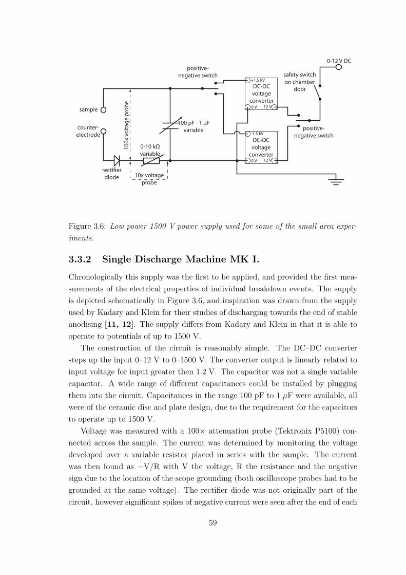
-1.5 kV
0 V 12 V
sample
counter-electrode
0-10 kΩvariable
100 pF - 1 μFvariable
+1.5 kV
0 V 12 V
DC-DCvoltage
converter
DC-DCvoltage
converter
0-12 V DC
10x voltageprobe
100x
vol
tage
pro
be
rectifierdiode
safety switchon chamber
door
positive-negative switch
positive-negative switch
Figure 3.6: Low power 1500 V power supply used for some of the small area exper-
iments.
3.3.2 Single Discharge Machine MK I.
Chronologically this supply was the first to be applied, and provided the first mea-
surements of the electrical properties of individual breakdown events. The supply
is depicted schematically in Figure 3.6, and inspiration was drawn from the supply
used by Kadary and Klein for their studies of discharging towards the end of stable
anodising [11, 12]. The supply differs from Kadary and Klein in that it is able to
operate to potentials of up to 1500 V.
The construction of the circuit is reasonably simple. The DC–DC converter
steps up the input 0–12 V to 0–1500 V. The converter output is linearly related to
input voltage for input greater then 1.2 V. The capacitor was not a single variable
capacitor. A wide range of different capacitances could be installed by plugging
them into the circuit. Capacitances in the range 100 pF to 1 µF were available, all
were of the ceramic disc and plate design, due to the requirement for the capacitors
to operate up to 1500 V.
Voltage was measured with a 100× attenuation probe (Tektronix P5100) con-
nected across the sample. The current was determined by monitoring the voltage
developed over a variable resistor placed in series with the sample. The current
was then found as −V/R with V the voltage, R the resistance and the negative
sign due to the location of the scope grounding (both oscilloscope probes had to be
grounded at the same voltage). The rectifier diode was not originally part of the
circuit, however significant spikes of negative current were seen after the end of each
59

discharge event, despite positive polarisation of the sample. The diode was included
to suppress this behaviour, which was likely a resonance relating to the capacitance
and the comparatively large change in current once an event has initiated.
The low power output of the DC–DC converter used, just 1.5 W continuous,
meant that the voltage across the sample could not be sustained once an event
initiated. The parallel capacitance in the circuit served as a store of charge and
energy which could be supplied to breakdown events. Even with a large capacitance
in parallel, the terminal voltage on the supply always drops when a breakdown
event initiates (see Figure 6.4). This is due to the high internal resistance of the
converter, and the large change in resistivity of the load from > 105 Ω with no active
discharge to ∼ 104 Ω when the discharge current peaks (see Figure 5.4). The size of
the voltage drop over the course of a discharge event could be reduced by increasing
the capacitance, but never totally removed (see Figure 6.4).
The drop in voltage during breakdown events, typically in the range from 8 to 100
V, will naturally have an effect upon the measured electrical characteristics of the
discharge events. Initially, the intention was to perform experiments on different
coating thicknesses using a series of increasing capacitances, to see whether the
measured properties reached limiting values as the capacitance was increased. As
will be discussed in chapter 5 and chapter 6, the interpretation of the data was not
quite so simple.
3.3.3 Single Discharge Machine MK II.
The second single discharge supply used was a combination of a commercial 650 V,
200 mA supply (FUG Elektronik MCP-140-650MOD) with a simple RC circuit. The
circuit is practically identical to the first supply, with a parallel capacitance and a
variable resistor to measure the current. The arrangement of the oscilloscope probes
was different in this case however, and the voltage over the current monitoring
resistor has to be subtracted from the voltage measurement to obtain the potential
difference across the sample. The other change is the inclusion of a 50 kΩ variable
resistor between the supply and the capacitor. This can be set to prevent the power
supply from being overloaded when a breakdown event initiates. The voltage over
the sample still drops, however the terminal voltage on the supply remains constant.
The voltage output and current limit of the supply were controlled using an
analog controller linked to the signal generator on the Picoscope 5203. The power
supply was also safety interlocked via the analog controller. The arbitrary waveform
generator on the Picoscope could in theory be used to control the supply voltage
output, however in practice the slow response time of the power unit means that
control at frequencies more then a couple of hertz is not viable. A limitation with
60

sample
counter-electrode
0-10 kΩvariable
100 pF - 1 μFvariable
10x voltageprobe
100x
vol
tage
pro
be
rectifierdiode
0-50 kΩvariable 0-650 V DC
Figure 3.7: Additional circuitry used in conjunction with a 650 V, 200 mA, power
supply used for some of the small area experiments.
this supply is that it only goes up to 650 V, minus any drop in potential across the
50 kΩ resistor.
3.4 Single discharge experiments performed.
Two experiments will be discussed in this work. The first resulted in a large dataset
which will be analysed and discussed in detail in chapter 5 and chapter 6. The
second did not result directly in useful data on discharge event properties, however it
was required in order to correct the data from in-situ monitoring. As was mentioned
in section 3.2, the current probe used electromagnetic induction to generate a signal,
and suffered from signal distortion when applied to measuring one-off pulses like
the discharge events. By recording the current signals from discharge events more
directly without this distortion, and concurrently recording the signal from the
current probe with distortion, a correction procedure could be produced.
3.4.1 Coating thickness and test circuit capacitance effects.
This experiment applied single discharge testing to seven different thicknesses of pre-
deposited coating. This was to investigate changes in discharging behaviour with
variation of the coating thickness. The different capacitances were used as it was
initially felt that discharge event properties would saturate at physically limiting
values of the system as the capacitance was increased. The actual behaviour was
markedly different, and will be discussed in chapter 5 and chapter 6.
61

6 mins 12 mins 18 mins 24 mins 30 mins 36 mins 42 mins
637 Ω 509 Ω 464 Ω 340 Ω 279 Ω 279 Ω 233 Ω
Table 3.3: Resistances used for current monitoring during single discharge testing
with a range of capacitances and coating thicknesses.
Samples were produced by coating rectangular sheets of aluminium 2024 alloy,
of dimensions 38 by 45 mm and 1 mm thickness. Two samples were coated for each
time of 6, 12, 18, 24, 30, 36 and 42 minutes. The substrates were coated using
the 50 Hz machine detailed in section 3.1 using an initial RMS current density of
1500 A.m−2.
Once coated, the samples were prepared for testing by attachment of 8 sections of
PVC tubing to one of the large flat coated surfaces, as described in subsection 3.3.1.
Seven wells on each sample were then used for single discharge testing, with a
different capacitance for each. The seven values used were 5.5, 14.3, 33.3, 100, 200,
500 and 1000 nF, spaced roughly equally on a base ten logarithmic scale. The 8th
test well was used as a test to determine an appropriate setting for the current
measurement resistor. The electrolyte used for the single discharge testing was a
sample of the electrolyte from the processing tank, which had been stored after all
the substrates had been coated.
Each combination of coating thickness and capacitance therefore had two re-
peats. Each test was conducted for a total period of 60 s after initiation of dis-
charging. The testing was broken down into 10 s segments. During each 10 s
segment the current and voltage were recorded at 1 MHz using a Picoscope 5203
oscilloscope controlled from a laptop computer. The data obtained was analysed
according to the procedures detailed in Appendix A.
The resistance of the variable resistor used to measure the discharge current was
different for each different thickness of coating, details of the test resistances used
are presented in Table 3.3. Different values were used to obtain a signal across the
monitoring resistor in the range 0–20 V for all thicknesses of coating tested. As will
be shown later in section 5.2, these resistances were all well below the minimum
resistances of typical discharge events, and so loading effects of the test resistor
would not be expected to be significant.
Test wells were only attached to one 38 by 45 mm side of the coated samples,
and the other coated side was reserved for microscopy of the coating free surfaces,
and sectioning to determine the coating thickness.
62

3.4.2 Generation of dataset for calibration of in-situ current
probe.
The data used to calculate the correction to be applied to the current probe data
was generated using the power supply detailed in subsection 3.3.3. The electrolyte
used was the same electrolyte as for all other experiments. The test coating used
was a 153 by 101 by 1 mm aluminium 1050 sample, coated for 10 minutes. It was a
spare from a different experimental set, the results of which will not be included in
this work. Three of the test wells on this sample were used to generate calibration
data.
Recording of data was at 500 kHz, for 5 segments of 20 s each, and for each
of the three test wells used. One channel of the oscilloscope recorded the voltage
over the variable resistor, set to 200 Ω, the other channel recorded the data from
the Tektronix P6021 current probe. Four loops of the signal wire, in series with the
measurement resistor, were passed through the current probe. This was in fact the
exact same coil as was used for in-situ monitoring experiments.
This dataset then comprised two sets of measurements of the same current sig-
nal. The current measured from the variable resistor had no distortion, and was
compared to the current probe data to produce a correction function for the in-situ
data. The procedure for this is discussed in Appendix B.
3.5 Microscopy and sample preparation.
3.5.1 Cold mounting of samples
Cold mounting was used for two purposes. Firstly to mount samples for sectioning
and microscopy, and secondly to create the samples for in-situ discharge monitoring
experiments. In both cases the system used was a commercial 2 component liquid
acrylic resin sold under the brand name Epofix. The two liquids were mixed in
disposable plastic beakers inside the hood of a fume cupboard. The pot life of the
mixture is long, as the resin takes ∼ 24 hours to cure at room temperature. The
resin is transparent when set, and shows low volume contraction upon curing. The
samples to be embedded were placed inside pre-greased rubber moulds for easy
extraction of the set samples. When the sample was to be used for microscopy, the
moulds were placed inside a sealed container and cycled between atmosphere and
vacuum several times to remove air bubbles in the resin that were introduced while
stirring the resin mixture.
63

3.5.2 Hot mounting of samples.
When the samples to be mounted were not likely to be damaged by heat or suffer
from significant thermal mismatch with the mounting resin, hot mounting presses
were used to mount samples for examination. The presses used were a Buehler
Metaserv and a Buehler Simplimet, and the powdered resin used was either trans-
parent or conducting, depending upon the requirement for the specific sample.
3.5.3 Sample sectioning.
When it was required to cut a section through a sample mounted for microscopy, this
was performed using a Struers Secotom-10 precision saw. Typical cutting speeds
in the range 0.005− 0.03 mm.s−1 were used, with a 2200 RPM alumina wheel of
thickness ∼ 1 mm. The saw had a computerised micrometer mount for accurate
positioning of the sample prior to sectioning. The same saw was used to cut 3–
4 mm off the ends on samples for in-situ monitoring between experiments, to expose
a fresh surface for subsequent experimental runs.
3.5.4 Polishing procedures.
Polishing procedures vary much depending upon the application and personal pref-
erences. It was found that the following procedure provided adequate surfaces for
microscopy. The samples were first ground with SiC papers, starting with 500
grade; then 800; then 1200 and finally 4000 grade. Between moving to the next
grinding stage the samples were briefly inspected by optical microscope to confirm
the removal of large scratches from the previous stage. Following grinding, the sam-
ples were polished using first 6 µm and then 1 µm diamond suspensions, applied to
the polishing cloth in aerosol form. Soft polishing cloths were not used, owing to
the tendency for the softer substrate to be preferentially removed by the polishing,
meaning the coating and substrate were not at the same height. Alcohol based
lubricant was used for polishing, and water for the grinding stages.
3.5.5 Optical microscopy.
Optical microscopy was performed using Olympus BHM and Zeiss Axiolab micro-
scopes, each fitted with a Moticam 1000 digital camera connected to a PC. De-
termination of scales in the images was performed using images captured with the
same systems of a calibration graticule.
64

3.5.6 Scanning electron microscopy.
Free surfaces of coatings were examined by scanning electron microscopy in sec-
ondary electron mode. A JEOL 5800LV SEM and a JEOL 6340F FEGSEM were
used for this purpose. No complications to usual SEM procedures were experienced,
with the exception of samples embedded in cold mounting resin (such as the in-situ
samples). Such samples required exposure to vacuum in a separate system for up to
24 hours prior to examination by SEM, in order to thoroughly outgas any residual
volatiles.
3.6 Processing of data.
A major challenge in this project was to develop computer procedures to reliably
identify and measure the discharge events recorded during experimentation. In
total across both in-situ and single discharge experiments approximately 5 million
individual discharge events were measured, this quite clearly was not done manually!
As with any automated data analysis, it is important to understand how reliable
the analysis is, and what the limitations may be. However, the general reader may
not be interested in the precise functioning of the algorithms used. To this end a
brief description of the functions of data handling algorithms will be given here,
along with a few figures to illustrate the algorithm functions. A detailed discussion
of each part of the data processing is provided at the end of this text in Appendix A
for single discharge data and Appendix B for in-situ monitoring. The procedures
were different due to the baseline correction required for the current probe data
from in-situ experiments.
3.6.1 Analysis of single discharge data.
A sample of the single discharge data obtained is presented in Figure 3.8. The short
lived current peaks corresponding to discharge events can be clearly seen, separated
by periods of low baseline current (∼ 1 mA). The slight decrease in voltage over each
event can also be seen in the figure. One of the events appears to be a superposition
of at least two current peaks. Such multiple peak events probably correspond to
two spatially separate discharge events that happen to overlap in time. Such multi-
peak events were common for some combinations of low coating thickness and high
circuit capacitance.
For analysis of discharge event properties, it is desirable to only consider events
comprised of a single current peak. To this end, the computer processing is required
to outline not just the start and end points of discharge events, but also the number
65

0
0.005
0.01
0.015
0.02
0.025
0.03
0
100
200
300
400
500
600
0 200 400 600 800
Current / A Voltage / V
Cu
rre
nt / A
Volta
ge
/ V
Time / µs
Figure 3.8: Sample current and voltage data from single discharge experiments,
taken from an 18 minute coating tested with 200 nF circuit capacitance.
of discrete current peaks within each event. Detailed discussion of the procedures
used can be found in Appendix A.
Procedures were developed which allowed for the automated estimation of the
baseline current level, Ibase, and a current threshold value, Ishift. These were used to
identify regions of interest. These regions of interest were expanded by a combina-
tion of procedures involving local current, voltage and current gradient thresholds,
until discharge events were indexed from initiation to termination. The discharge
locations were indexed in a vector, G, which took the value 1 if that sample was
part of a discharge event, and 0 otherwise.
Two values of importance are Istep and Vstep. The data recorded by the oscil-
loscope is 8-bit, meaning that only 127 distinct values can be resolved between 0
and the maximum range set. The variables Istep and Vstep then represent the min-
imum detectable shift in current or voltage respectively. Vstep was 7.87 V for all
data, and Istep varied with the size of resistor used, according to the expression
Istep = (20/127) /R, with R the resistance used. The value of 20 is present as the
current data was recorded from 0–20 V across the measurement resistor.
The positions of internal peaks and troughs within each outlined region were
indexed in the vector F . This variable took the value 1.0 at current peaks, and
0.5 at troughs. A peak, or trough, was defined relative to the scale of the event in
question. If the maximum current during an event is Imax and the minimum Imin,
66

0
0.005
0.01
0.015
0.02
0.025
0.03
0.2
0.4
0.6
0.8
1
1.2
0 200 400 600 800
Current / A Logical index GInternal index F
Cu
rre
nt / A
Lo
gic
al in
dex G
Time / µs
Figure 3.9: The representative section of experimental data, showing current, logical
indexing vector G and internal peak indexing vector F .
then the scale of variation required for a peak or trough to be identified was the
larger of 0.2 × (Imax − Imin) or 5 × Istep. The final results of indexing procedures
are demonstrated for the same section of data as in Figure 3.8 in Figure 3.9.
Once events had been indexed and listed, measurements could be made of the
discharge event properties. The data was first separated into two lists, one contained
all indexed discharge events, the second only events comprised of a single current
peak. It is primarily the latter dataset which will be of interest. Important mea-
surements that were made included the peak current, Ipeak; the initiating voltage,
Vinit; the duration, dsing; the peak power, Ppeak; the charge, Qsing, and energy, Esing,
associated with each event. The charge and energy were calculated from trapezium
rule integration over the event duration, and the baseline current was subtracted
from the current values prior to any calculations. Other measurements were made,
and are detailed in Appendix A, however those mentioned in this section are those
of greatest interest.
It should be borne in mind that no events were included which showed a value
of Ipeak less than 5× Istep. Also, the minimum error on currents is Istep, on voltages
is Vstep and in time, the indexing is not accurate to more than plus or minus the
sampling interval of δt = 1× 10⁻⁶ s.
67
3.6.2 Analysis of in-situ monitoring data.
Procedures for the in-situ data are broadly similar, as the events being indexed are
essentially the same. Before any events can be indexed however, the signal from the
current probe must be corrected for the distortion of the baseline level. The data
obtained as described in subsection 3.4.2 was used to directly calculate a frequency
response function relating the signal from the current probe to the actual current (as
measured by the voltage over the 200 Ω resistor). The discussion in this section will
not go into many details, and the interested reader can find a complete description
of the data processing for in-situ experiments in Appendix B.
The current peak associated with a discharge event can be viewed as a wave-
packet, and as such it will contain amplitude across a wide range of frequencies.
Some of the signal amplitude will be at frequencies below the frequency cut off
of the current probe, and it is the distortion of these low frequency components
which leads to the distortion of the signal. Once the frequency response had been
calculated using the calibration data, the current probe signal from each process
cycle could be readily corrected.
This involved isolating the period of positive polarity during each cycle in the
in-situ monitoring records, then applying the fast Fourier transform to compute the
discrete Fourier transform of the current data. The current signal in the frequency
domain is then multiplied at each frequency by the corresponding value of the
frequency response function. Application of the inverse Fourier transform brings
the signal back into the time domain.
An example of the correction procedure, as applied to a section of the calibration
data (so the corrected current can be compared to the resistor based measure) may
be found in Figure 3.10. The current measured from the resistor and from the
current probe are both plotted, as is the corrected signal from the current probe.
The agreement seen is good, but of course it is far from perfect, and this leads to
a greater level of uncertainty when compared to the single discharge data. On the
other hand, the in-situ data is a closer analogy to actual PEO processing, and so the
data obtained is more representative than that from single discharge experiments.
An example of the in-situ experimental data, and the corrected small area cur-
rent, is plotted in Figure 3.11. There does appear at first to be a slight problem
with the correction, in that the data seems to be superposed on a low ‘hump’. This
‘hump’ is real however, and probably corresponds to a non-discharge component
of current (see Appendix B). The rough signal in the region preceding the large
discharge events is not noise, and typically is only present in the early part of each
process cycle. It could be small discharge events that are poorly resolved using the
parameters used for the bulk of the in-situ work. The presence of very small dis-
68

-0.005
0
0.005
0.01
0.015
0.02
0.025
0.03
0.035
0 50 100 150 200
Current (resistor)Current (probe)Current (corrected probe)
Cu
rre
nt / A
Time / µs
Figure 3.10: Section of calibration data showing the current measured via a known
resistance, using the current probe, and the corrected current probe signal.
charges, and discharges during negative polarisation of the sample, will be discussed
in section 4.3 and section 4.4 respectively.
Once the baseline level has been corrected, a series of routines broadly similar
to the single discharge case are applied to identify the discharge events and measure
the relevant properties. The indexing of the large events seen in Figure 3.11 can
be seen in a zoomed-in view in Figure 3.12. The internal indexing of multiple peak
events is also performed, though multi-peak events were rarer than for the single
discharge experiments. This is probably a result of the much smaller area being
monitored in this case.
The event properties are then calculated from the indexed discharge events.
The same properties as were outlined in subsection 3.6.1 were calculated for in-situ
monitoring data, and the data was again broken down into all events, and the subset
which displayed a single current peak. One important difference is in the range of
events included; only events which exceeded 10 mA base to peak were included.
This was because the hump like feature during every cycle, when combined with
the error incurred from the correction procedure, meant that a reliable indexing of
events smaller than about 6–8 mA was elusive.
The bar was set at 10 mA for safety, operating under the principle that it is
69

-0.04
-0.02
0
0.02
0.04
0.06
0.08
0.1
-200
0
200
400
600
0 500 1000 1500 2000 2500 3000 3500 4000
Current (uncorrected) / ACurrent (corrected) / A
Voltage / V
Cu
rre
nt / A
Volta
ge / V
Time / µs
Figure 3.11: Comparison of the uncorrected and corrected current signal for one
processing cycle. Note that the full period of positive polarity is not displayed to
allow better resolution of discharge features during the active period.
70

0
0.01
0.02
0.03
0.04
0.05
0.06
0.07
0.08
0
0.2
0.4
0.6
0.8
1
1.2
4500 5000 5500 6000
Current / A Logical index G
Cu
rre
nt / A
Lo
gic
al in
dex G
Time / µs
Figure 3.12: Example of the completed indexing for a zoomed-in section of the ex-
ample cycle from Figure 3.11.
71
better to be able to trust a reduced range of application than to leave coverage
wider but unreliable. The reader should not forget though that the in-situ data
reported only relates to events larger then 10 mA. This is not an inherent limit,
and with small changes to this methodology the coverage can be extended down to
smaller discharge events. Some steps in that direction have been taken, and will be
discussed in section 4.3.
3.6.3 Averaged development profiles of discharge events.
The average current at times after the initiation of a discharge event was also
calculated, for both single discharge and in-situ data. The calculation of average
current development profiles was broken down by initiating voltage and duration.
For example, if we wanted the average current profile for an event initiated at 520 V,
which lasted for 50 µs, the algorithm would locate every discharge event which met
those two criteria. Then for every time point between initiation and termination
it would calculate the mean and standard deviation of the current at that time
point after initiation, using all the events which met the criteria as a sub-dataset.
This allows a reasonable measure of the average ‘shape’ of discharge events to be
estimated.
As mentioned previously this was done for each combination of Vinit and dsing.
This was performed for both the current and the voltage during discharges, and
corresponding standard errors were also calculated. Full details may be found in
Appendix A, and examples of the procedure output will be presented and discussed
throughout chapter 6.
72

Chapter 4
Evolution of Discharge Events
During Coating Production.
4.1 In-situ monitoring with scaling of monitored
area.
The results of in-situ monitoring experiments can provide much information about
the process, however it must first be considered just how representative the data
from the small area can be of the wider PEO process. To this end, before the results
of individual discharge measurements are presented, the processing of the small area
will be discussed in more conventional terms.
4.1.1 Coating development on the small area.
As the small area was processed to longer times, the coating increased in thickness
as is normal for PEO processing. What was different was that the scale of the small
area exposed to processing was not constant. This arose from the progressive failure
of the resin in which both small and large areas were mounted.
At the edges where the substrate was in contact with the resin, any discharge
event which occurred would cause local destruction of the shielding resin. This
would in turn expose more of the substrate wire to the electrolyte. An example cross
section can be seen in Figure 4.1. The destruction of the resin and the penetration
of processing down the sides of the substrate are evident in the figure.
It is worth noting that whilst the polymeric resin failed in this fashion, it has
better performance than might be expected. A chemically setting and low temper-
ature curing ceramic cement containing TiN was also tried (Ceremabond 865 from
Aremco). Though such a material has a higher operating temperature (1923 K),
and so might be expected to perform better than the resin, the thermal shocking
73
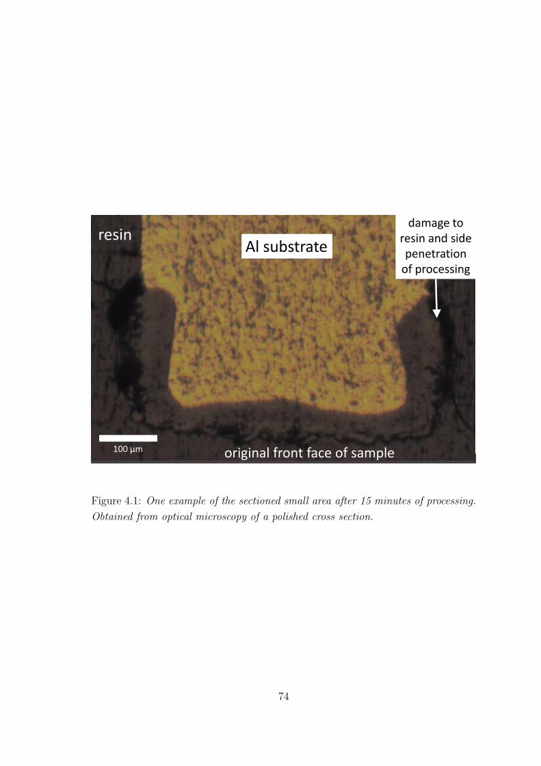
100 µm
resinAl substrate
damage toresin and sidepenetration
of processing
original front face of sample
Figure 4.1: One example of the sectioned small area after 15 minutes of processing.
Obtained from optical microscopy of a polished cross section.
74

0
20
40
60
80
100
0
100
200
300
400
500
600
0 10 20 30 40 50
Small areaLarge area
Small area side penetration / µm
Co
ating
th
ickn
ess / µ
m
Sm
all a
rea
sid
e p
en
etra
tion
/ µm
Time / mins
Figure 4.2: Development of coating thickness on small and large areas with process-
ing time. Determined from examination of polished optical cross sections.
associated with the discharging behaviour caused the ceramic shielding material to
rapidly fail by cracking.
4.1.2 Thickness development and surface appearance.
As samples were sectioned for every 5 minute period of processing up to 40 min-
utes, the development of the coating thickness on the small and large areas can
be determined and compared. The progressive failure of the sample shielding can
also be examined. These properties are plotted in Figure 4.2. The small area coat-
ing thickness seems to develop at a slightly faster rate than the thickness on the
large area at long times, but the main discrepancy is within the first few minutes.
The thickening rate in the very early stages of processing must therefore be signifi-
cantly larger for the small area. Both thicknesses display the linear coating growth
expected for 50 Hz PEO processing, as was discussed in subsection 2.3.1.
The progression of shielding side penetration is less regular than that of the
thickness, but still shows a clear trend with coating time. The initial period of
processing again shows faster progression. A linear fitting to the side penetration
data can then be used to estimate the total size of the small area exposed to the
electrolyte, being the original area plus the additional area in the form of a cylinder
exposed by degradation of the resin shielding.
Before moving on to utilise the small area variation estimate, the surface appear-
75

a) b)
c) d)
Figure 4.3: SEM images of the coating free surfaces after a) 5, b) 15, c) 25 and d)
35 minutes.
ances of the PEO coatings deposited on the small monitored area shall be briefly
considered . SEM images of the coating free surface are presented in Figure 4.3.
The surface morphologies are seen to be typical for PEO processing of aluminium.
4.1.3 Comparison of charge delivered to small and large
areas.
The surface structures are typical of PEO coatings on aluminium (see subsec-
tion 2.3.2). How representative the small area is of the bulk processing of the
wider sample is yet to be made clear. This can be examined by using the estimates
of total exposed area, derived from a linear fitting to the progressive shielding pene-
tration plotted in Figure 4.2. The charge delivered per positive cycle, per unit area,
for both the small and large areas is plotted in Figure 4.4. This figure was compiled
from averaging across all the samples in the set Al 01 to Al 05, and all experimental
runs (see subsection 3.2.1). Average values for each 150 s process section are what
is plotted. Large area charge delivered was calculated from the experimental runs
which logged bulk current (see Table 3.2). The charge per cycle per unit area is
76

0
10
20
30
40
50
0 10 20 30 40
small arealarge area
Ch
arg
e p
er
po
sitiv
e c
ycle
per
un
it a
rea
/ C
.m-2
Time / mins
Figure 4.4: Plots of the charge per positive cycle per unit area delivered to small
and large areas.
elevated for the small area at all times, and is particularly pronounced for about
the first 20 minutes of processing. This appears to be in good agreement with the
relative thickening rates observed.
From the consideration of thickening rates in Figure 4.2 and charge delivered in
Figure 4.4, is is apparent that the small area is not entirely representative of the
bulk processing behaviour. However the information indicates that what is seen on
the small monitored area represents PEO processing at a current density that is
slightly enhanced with respect to the rest of the substrate.
4.1.4 Cumulative charge of indexed discharge events.
An important test of whether the data can be taken as representative of the wider
sample is whether or not the discharge activity seen scales with the size of the
monitored area. We would expect that the discharging activity on the samples
Al 03 and Al 04 with two 500 µm wires as small area would be approximately
twice that seen for the samples with only one wire, Al 01 and Al 02. The sample
with three wires, Al 05, would be expected to show approximately three times the
activity.
One way to visualise the discharging activity is to plot the cumulative charge
77

delivered by indexed events against the time of processing. This may be done for
each distinct experimental run. No two experimental runs are the same, as at any
given point the discharging occurs in a stochastic and unpredictable fashion with
such small areas. However when many experimental runs are plotted in this fashion,
as in Figure 4.5 and Figure 4.6, the overall trends become more evident.
In can be seen most clearly in Figure 4.5 panel a) that discharging activity on a
small scale does not occur in a continuous fashion. Rather it occurs in interspersed
periods of high and low discharging activity. This can also be seen in the samples
with 2 or 3 wires as the small area However the larger area being monitored increases
the probability of one of the sampled areas being active at any given point. This
leads to cumulative charge plots which are more continuous in appearance and which
appear to show less variation between experimental runs.
Panel b) of Figure 4.6 plots the averages of all continuous experimental runs
for each of the 1 wire, 2 wire and 3 wire samples. The average plots for 2 and 3
wire samples are also plotted normalised by division by a factor of either 2 or 3
as appropriate. From the normalised plots it can be seen that with two wires as
the small area, the cumulative charge in discharges increases approximately twice
as rapidly, and with three wires the rate of increase is tripled. This is not exact
however, and the 2 wire normalised plot is higher then the single wire average.
The triple wire data is again slightly above the double wire values. This slight
enhancement over that expected is possibly due to edge effects, known to increase
discharging intensity around the edges of samples.
4.1.5 Discharging rates.
The data on cumulative charge with processing times appears to support the con-
clusion that the discharging activity scales with the area being monitored. Further
evidence is provided by analysis of the overall rates of recorded discharges, plotted
in Figure 4.7. This demonstrates that the discharge activity seen does scale with
the size of the area monitored.
When combined with the information in Figure 4.2 on thicknesses and Figure 4.4
on the charge transfer per process cycle, it is possible to state that the information
gathered from in-situ monitoring of a small area can be taken to be representative of
the wider bulk processing. Subject of course to the condition that the experiment be
repeated a sufficient number of times, due to the stochastic nature of the discharging
behaviour.
Having demonstrated that the discharging activity scales with the size of area
monitored, no distinction will be made in the following discussions between data
obtained from experimental runs with single, double or triple wire samples. All
78

0
0.05
0.1
0.15
0.2
0.25
0.3
0.35
0 500 1000 1500 2000 2500
1 wire samples
run 1run 2run 3run 4
run 5run 7run 8run 6
Cu
mu
lative c
ha
rge tra
nsfe
rred
/ C
Time / s
0
0.1
0.2
0.3
0.4
0.5
0.6
0.7
0.8
0 500 1000 1500 2000 2500
2 wire samples
run 1run 2run 3run 4
run 5run 6run 7run 8
Cu
mu
lative c
ha
rge tra
nsfe
rred
/ C
Time / s
(a)
(b)
Figure 4.5: Cumulative charge delivered by indexed discharge events for multiple
experimental runs for (a) 1 wire samples and (b) 2 wire samples.
79

0
0.2
0.4
0.6
0.8
1
1.2
0 500 1000 1500 2000 2500
3 wire sample
run 1run 2
run 3run 4
Cu
mu
lative c
ha
rge tra
nsfe
rred
/ C
Time / s
0
0.2
0.4
0.6
0.8
1
0 500 1000 1500 2000 2500
sample averages
1 wire averaged2 wires averaged3 wires averaged2 wires normalised3 wires normalised
Cu
mu
lative c
ha
rge tra
nsfe
rred
/ C
Time / s
(a)
(b)
Figure 4.6: Cumulative charge delivered by indexed discharge events for multiple
experimental runs for (a) 3 wire sample and (b) sample averages and normalised
plots.
80

0
5 107
1 108
1.5 108
2 108
2.5 108
3 108
3.5 108
4 108
0 5 10 15 20 25 30 35 40
single wiredouble wiretriple wire
Dis
ch
arg
e r
ate
/ .s
-1.m
-2
Time / mins
Figure 4.7: Average discharging rates as events per unit time per unit area for in-
situ samples with a single, double or triple 500 µm wire as the small area. Rates
are an average of the total number per unit time over the 2.5 minutes prior to the
marked point.
81

events recorded at a certain time into processing will be taken together to be rep-
resentative of that time period, once they have been combined to produce average
values and distributions.
Before proceeding to discussion of the single event properties, it is worth placing
the discharging rates per unit area plotted in Figure 4.7 within the context of the
literature values for discharge rates. The rates derived from low speed optical
imaging studies are found to be a factor of ten lower than in the present work
at equivalent durations of processing [2, 7, 8, 9]. This is probably because the
imaging speed in these works was insufficient to capture the discharging behaviour
accurately when clustering of discharge events in considered.
For some of the alloys they tested, the data from the high speed study of Arra-
bal et al is in order of magnitude agreement with the present work, at around
108 m−2.s−1 [5]. Values up to the order of 109 m−2.s−1 were reported in the same
work, and this shows that the difference between different substrates could be pro-
nounced in some cases.
4.2 Properties of individual events recorded
during in-situ monitoring of the PEO process
and variation with processing time.
The properties of events seen at any given point in time were observed to vary over
a wide range. Given this, to calculate mean event properties would be to omit most
of the important details of the discharging behaviour. The rates of discharging
behaviour were also decreasing with processing time. In order to account for the
variation of event properties seen at any time, for the statistical spread of measured
properties and also for the variations in discharging rate, a specific form of plot will
be used to present the single discharge data.
These plots will be of the 10th to the 90th percentiles of the data in each time
region. The width of time regions will vary to ensure that there are 50 000 measured
events during each time region. The plots will be in the form of step plots, which
make the width of each time region clear, in addition to the value of the relevant
percentile of the measured event property at that time.
At no time should the reader forget that the measured properties refer only
to those events which exceeded 10 mA from base to peak, and for which the data
was processed as described in Appendix B. Furthermore, whilst 2 666 611 events
were indexed in total across all experimental runs with the samples Al 01 to Al 05,
only 2 351 508 were in the form of individual events which occurred during process
82

500
520
540
560
580
600
620
0 500 1000 1500 2000 2500
10th20th30th40th50th60th70th80th90th
Event
initia
ting v
oltage /
V
Time / s
Figure 4.8: Variation of the distribution of Vinit with time of processing. Variable
step length indicates the diminishing rate of discharging.
cycles in which the current probe signal was less then the maximum range. These
represented 98.53% of all single peak events, the remaining 1.47% having occurred
during process cycles in which the maximum current range set on the oscilloscope
(100 mA) was exceeded. Current data from such cycles could not be properly
corrected for the baseline distortion due to truncation of one or more peaks.
4.2.1 Event initiating voltages.
The event initiating voltages, Vinit, will be considered first, and the distributions
can be seen plotted in Figure 4.8. The step-like appearance of this plot is due to
the 8-bit nature of the original voltage data, with Vstep = 7.87 V . At all times
the shape of the distribution is seen to be asymmetric, with greater width down to
lower voltages, and rapid drop off in the distribution above the median.
The rate of increase of Vinit slows between 700 to 1000 s into processing. At
about the same time the width of the distribution is seen to increase. Whether
these slight changes in the Vinit distribution are significant is hard to say, as it
cannot be determined from this data alone whether the changes are due to the
processing or the equipment used.
What is clear from the Vinit distributions presented in Figure 4.8 is that discharge
83
events are initiated across a range of applied voltages at all times of processing. This
distribution moves upwards in voltage as the coating thickens, but as can be seen
from comparison with Figure 4.2, this increase is not in proportion to the coating
thickness.
4.2.2 Discharge event peak current.
The peak current reached by discharge events, Ipeak, is a key measure of discharge
scale and intensity. It also offers an opportunity for comparison with the literature
records. The distributions of Ipeak with processing time are plotted in Figure 4.9.
The distributions are seen to be relatively broader than for Vinit, with a noticeable
shift in both distribution width and median value around 700 to 1000 s into pro-
cessing. Beyond 1000 s there is no significant increase in the median value of Ipeak,
with the only change being a gradual widening of the distribution.
This shift in the distribution occurs at around the point in processing when it
was observed that the visual appearance of the processing undergoes a noticeable
change. The change seen through this period is from a blue-white appearance of
the discharges to a more orange-yellow character. Such a transition has often been
reported in the literature [2, 7, 9, 16, 17]. Whether the shift in the median
and distribution width of the discharge peak event currents is related to such an
apparent change in visual appearance is not possible to say conclusively.
One point of interest from Figure 4.9 is that the low current end of the Ipeak
distribution never shows any significant increase over the duration of processing.
It should also be remembered that the distribution has been artificially curtailed
at 10 mA, and so probably continues down to lower values of the discharge peak
current for all times. The implication of this is that whilst the largest discharges,
and the discharges on average, show increased current as the coating thickens, the
smallest events remain of a similar scale throughout.
The range of currents seen in Figure 4.9 is from the cut off at 10 mA up to
110 mA. Referring back to Table 2.2, such values are in agreement with quoted
literature values for the scale of discharge currents [10, 13, 19, 23]. The advantage
of the in-situ monitoring dataset over the literature values is that the present work
provides much more information than just an order of magnitude. The great variety
of values seen at all process times underlines the requirement for datasets of PEO
discharge properties to be presented as statistical distributions, based upon large
numbers of measurements. In fact examination of Figure 4.9 suggests that still
further repeats would be of value.
84

0
0.02
0.04
0.06
0.08
0.1
0.12
0 500 1000 1500 2000 2500
10th20th30th40th50th60th70th80th90th
Peak e
vent
cu
rrent /
A
Time / s
Figure 4.9: Variation of the distribution of Ipeak with processing time.
4.2.3 Discharge event durations.
Distributions of the discharge event durations, dsing, may be found in Figure 4.10.
The form of the distributions is broadly similar to that of the event peak currents. A
shift in the distribution width and median value is again seen as 1000 s of processing
is approached, though in the case of the durations the median value sustains an
increase as the distribution widens with processing time beyond 1000 s. The lower
end of the dsing distribution does not display any trend with the coating thickness.
The values seen are from ≈ 30 µs up to almost 400 µs. Such values are in good
agreement with many of the studies summarised in Table 2.1. The major discrepan-
cies are from comparison with studies by Matykina et al [8] who reported discharge
durations in the hundreds of ms, and Golovanova and Sizikov [24] who reported
less than 7.5 ms, which was presumed to be an upper bound. The disagreement
with these studies is readily explained by the inappropriate measurement timebase
employed, and good agreement is seen with studies which had better temporal reso-
lution [5, 10, 13, 19, 21, 23]. For the higher end of the discharge current densities
considered by Yerokhin et al, they calculated ∼ 250 µs [2], also in good agreement
with the findings of the present work.
85

0
100
200
300
400
0 500 1000 1500 2000 2500
10th20th30th40th50th60th70th80th90th
Event
dura
tio
n / µ
s
Time / s
Figure 4.10: Variation of the distributions of dsing with processing time.
4.2.4 Peak instantaneous power levels.
It should not be surprising that the peak power, Ppeak, reached by individual dis-
charge events follows the trends of the Ipeak and Vinit distributions. The Ppeak
distributions are presented in Figure 4.11. The power levels are large, though gen-
erally not sustained for more then a few µs. If the discharge current is all passing
through a hole in the coating of similar dimension to the craters observed in the ex-
terior surfaces of PEO coatings (see subsubsection 2.3.2.2), then the power density
in the region of the discharge event will be very large.
The value of peak power quoted by Bao Van et al for one of the discharges they
observed was 35 W [13]. This value is well within the range seen in the present
dataset, and close to the median value beyond about 1000 s. The range reported
by Gordienko and Gnedenkov was 0.2− 1.0 W [23]. This is not within the range
of values plotted in Figure 4.11. The present dataset contains no information on
events less then 10 mA base to peak, however events spanning the range quoted
by Gordienko and Gnedenkov [23] were observed in the single discharge dataset,
discussed in chapter 5. Such small events do exist in the in-situ dataset, though
they are not resolved in the bulk of the results some information is available in
section 4.3.
86

0
10
20
30
40
50
60
70
0 500 1000 1500 2000 2500
10th20th30th40th50th60th70th80th90th
Peak e
vent
pow
er
/ W
Time / s
Figure 4.11: Variation of the distributions of Ppeak with processing time.
4.2.5 Charge and energy of individual discharges.
The distributions of both charge transferred, Qsing, and energy dissipated, Esing,
by individual events are little different in form and variation, following closely from
the Ipeak and Vinit distributions. The precise values are nevertheless of interest,
given the previous lack of information with regard to these properties. The Qsing
distributions are found in Figure 4.12 and the distributions of Esing values are
presented in Figure 4.13.
Typical events are seen to transfer from a few to a few tens of µC of charge.
Typical energy dissipation is from a few mJ to about 13 mJ. It should be borne
in mind that the precise volume within which this energy is dissipated will depend
upon such parameters as the electrolyte and plasma electrical conductivities, and
on the geometry of the event in terms of size and scale.
Few values are available in the literature for comparison, though Bao Van et al
reported the energy of a single measured event to be 2.9 mJ [13], which is in good
agreement with the distributions presented in Figure 4.13. Another value reported
by Kasalica et al was 0.2 µJ, much lower than typical values seen in the present
work [10]. The distribution of the event energy dissipations in the present work
does extend all the way down to ∼ 1 µJ however, so even this low value is not far
outside the range observed.
87

0
5
10
15
20
25
0 500 1000 1500 2000 2500
10th20th30th40th50th60th70th80th90th
Ch
arg
e t
ransfe
rre
d / µ
C
Time / s
Figure 4.12: Variation of the distributions of the Qsing with processing time.
0
2.5
5
7.5
10
12.5
15
0 500 1000 1500 2000 2500
10th20th30th40th50th60th70th80th90th
Energ
y d
issip
ate
d / m
J
Time / s
Figure 4.13: Variation of the distributions of Esing with processing time.
88

4.3 Small current (< 10 mA) events.
The limits applied to the data obtained by in-situ monitoring, in the form of the cut
off below 10 mA, are not inherent to the technique. Use of more sensitive detection
arrangements, and smaller monitored areas can allow for information about the
smallest events during PEO processing to be obtained.
As was described in subsection 3.2.1, one additional in-situ sample was produced,
using a single 120 µm wire as the small area. This sample was used for some limited
in-situ monitoring, and the coil passed through the current probe was increased from
four turns to ten, increasing the sensitivity of the current probe to 5 mV per 1 mA.
Experiments were also conducted at a faster logging rate of 62.5 MHz. A sample
of the data from this more sensitive version of the in-situ monitoring experiment,
from about 6 minutes into processing, is presented in Figure 4.14.
The data in Figure 4.14 has not had the frequency response correction applied.
This is as the fine detail would likely be lost during the process. The events captured
in this instance are small, meaning the effect of LR droop is minimal.
A selection of very low amplitude events is seen. Such events are commonplace
throughout the duration of PEO processing. Events this small could not be reliably
resolved in the original in-situ monitoring experiments, though they could be iden-
tified before and after the peak activity periods in some cycles. It is likely that the
500 µm wires used originally represented an area too large to ensure that no events
as small as those seen in Figure 4.14 initiated concurrently. This is I believe the
source of the ‘noisy’ region seen in many of the in-situ current traces. Though rel-
atively small, such events were numerous, and the discharges shown in Figure 4.14
still reach peak instantaneous powers in the range 1–2 W.
Whilst it is unfortunate that such detail was not resolved in the main experi-
ments, this data demonstrates that the capabilities of the technique go far beyond
what has been achieved so far. There is a trade-off however: although smaller areas
ensure that even the weakest of discharge events can be isolated, a great many more
repeats will be required before information representative of the wider processing
can be obtained.
4.4 Occurrence of electrical breakdowns during
cathodic polarisation of the substrate.
Using the same modified in-situ monitoring set-up described as for the data pre-
sented in section 4.3, observations of the current during cathodic polarisation of
the sample were made and are presented in Figure 4.15. It should again be noted
89

-0.5
0
0.5
1
1.5
2
2.5
3
3.5
0
100
200
300
400
500
600
0 40 80 120 160 200 240 280
Current / A Voltage / V
Cu
rre
nt / m
A Volta
ge / V
Time / µs
Figure 4.14: Example of the sensitivity which can be achieved for in-situ monitoring
experiments, taken from about 6 minutes into processing. Note that no correction
for the inductive effects of the current probe has been applied to this data.
90

-6
-4
-2
0
2
4
-100
-80
-60
-40
-20
0
20
40
60
0 100 200 300 400 500 600
Current / A Voltage / VC
urr
ent / m
A Volta
ge / V
Time / µs
Figure 4.15: Example of some apparent electrical breakdown events during cathodic
polarisation of the substrate, taken at a point about 3 minutes into processing. Note
that no correction for the inductive effects of the current probe has been applied to
these data.
that no frequency response correction has been made to this data, which is why the
baseline level shows distortion in the figure. There are features in the plot which
look very similar to the discharge events during positive polarisation of the sample.
Such discharging behaviour during the negative portion of the process cycle was
observed to be reasonably common during the the first 5–6 minutes of processing.
No such breakdown events during cathodic polarisation were seen beyond 7 minutes
into processing in the present work. Whilst no firm conclusions can be drawn based
on the available evidence, the indications are that electrical breakdowns do occur
during cathodic polarisation of the substrate during PEO processing, though it ap-
pears that such events are only seen in the very early stages of coating development.
91

Chapter 5
Single Discharge Experiments.
In this chapter the results of single discharge testing of coatings pre-deposited using
the 10 kW industrial supply detailed in section 3.1 are presented. Coatings were
produced to multiples of 6 minutes from 6 up to 42 minutes as detailed in subsec-
tion 3.4.1. The thickening rate of the pre-deposited coatings for single discharge
testing will be discussed first, followed by the experimental results obtained from
the experiments.
A series of increasing capacitances were used for each different thickness as it was
originally thought the discharge event properties such as peak current and duration
would increase with capacitance until they reached a saturation value which could
be regarded as representative of the large scale processing. As shall be described
below, this was not observed, however the technique proved useful nonetheless, and
fundamental aspects of PEO discharging behaviour were extracted from the data.
To briefly re-state, the circuit capacitances applied in parallel with the samples took
the values 5.5, 14.3, 33.3, 100, 200, 500 and 1000 nF, spaced roughly equally in the
values of logarithm base ten.
5.1 Coating thickness development.
Before considering the properties of individual discharge events recorded during the
experiments, the thickness and structure of the coatings used for single discharge
testing will be briefly considered. The coating free surfaces were examined by SEM,
one such image of a coating deposited for 30 minutes is presented in Figure 5.1. Such
images confirm that the coatings generated are regular PEO coatings, as described
in the literature (subsection 2.3.1).
The coating thickness was determined by optical microscopy of polished cross
sections. Several such cross sections were joined together by correlating the edges
until a region of coating just over 500 µm in length was in a single image. The
92
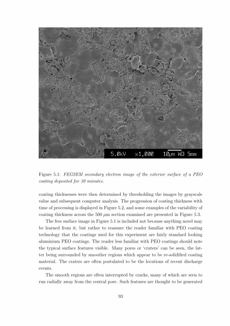
Figure 5.1: FEGSEM secondary electron image of the exterior surface of a PEO
coating deposited for 30 minutes.
coating thicknesses were then determined by thresholding the images by grayscale
value and subsequent computer analysis. The progression of coating thickness with
time of processing is displayed in Figure 5.2, and some examples of the variability of
coating thickness across the 500 µm section examined are presented in Figure 5.3.
The free surface image in Figure 5.1 is included not because anything novel may
be learned from it, but rather to reassure the reader familiar with PEO coating
technology that the coatings used for this experiment are fairly standard looking
aluminium PEO coatings. The reader less familiar with PEO coatings should note
the typical surface features visible. Many pores or ‘craters’ can be seen, the lat-
ter being surrounded by smoother regions which appear to be re-solidified coating
material. The craters are often postulated to be the locations of recent discharge
events.
The smooth regions are often interrupted by cracks, many of which are seen to
run radially away from the central pore. Such features are thought to be generated
93

0
5
10
15
20
25
30
0 6 12 18 24 30 36 42
Thickness /micronMaxMin
Th
ickne
ss /m
icro
ns
Time / minutes
Figure 5.2: Development of the coating thickness with time of processing for single
discharge samples. The line labelled thickness is the mean thickness, and the error
plotted represents standard deviation of the thickness. Minimum and maximum
thickness values observed are also plotted for reference.
94
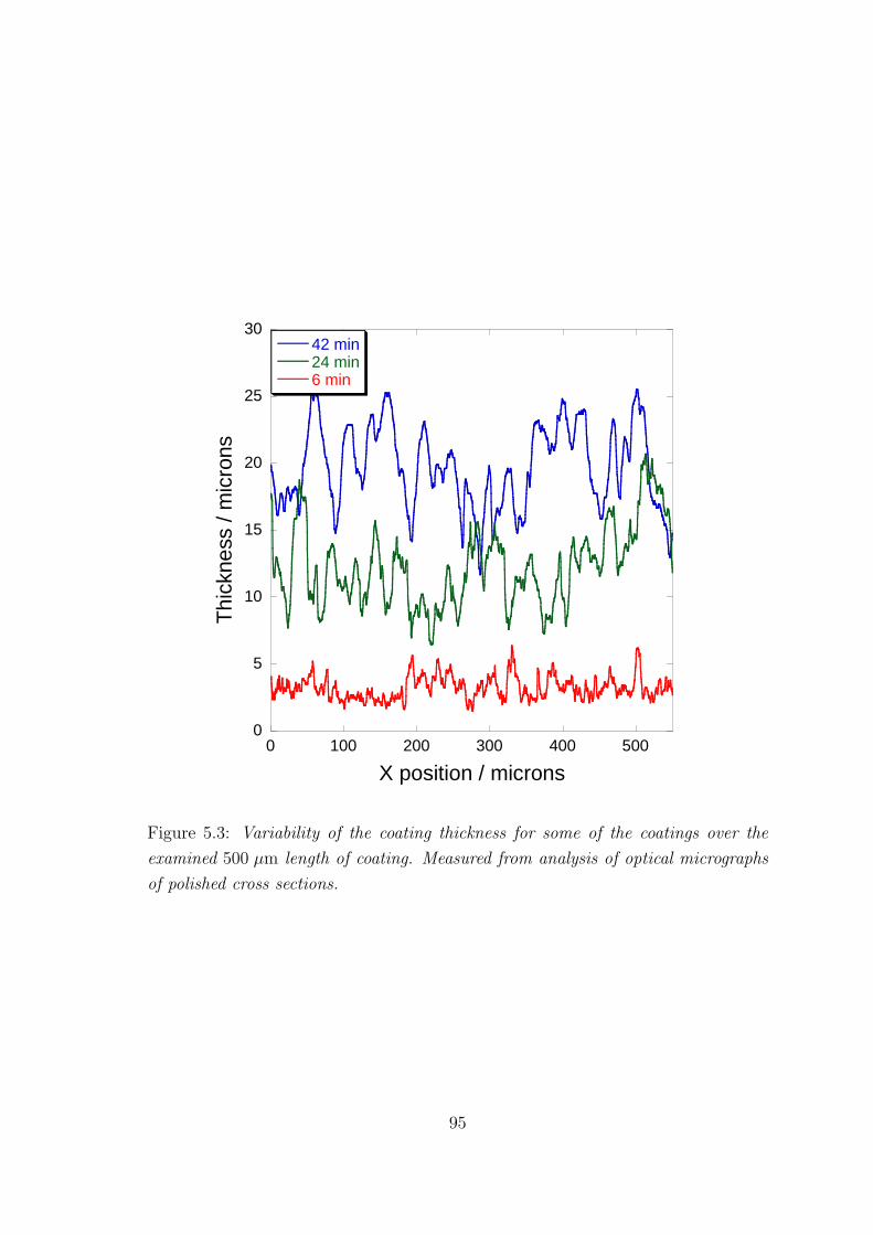
0
5
10
15
20
25
30
0 100 200 300 400 500
42 min24 min6 min
Th
ickne
ss / m
icro
ns
X position / microns
Figure 5.3: Variability of the coating thickness for some of the coatings over the
examined 500 µm length of coating. Measured from analysis of optical micrographs
of polished cross sections.
95

6 mins 12 mins 18 mins 24 mins 30 mins 36 mins 42 mins
637 Ω 509 Ω 464 Ω 340 Ω 279 Ω 279 Ω 233 Ω
Table 5.1: Resistances used for current monitoring during single discharge testing
with a range of capacitances and coating thicknesses.
by differential thermal stresses experienced during rapid cooling of the coating ma-
terial in the aftermath of a discharge event. The rougher material interspersed with
the smooth re-solidified patches is also penetrated by numerous pores. All of these
pores and surface cracks are thought to be connected to the sub-surface porosity
known to be present in PEO coatings at levels around 20% [6].
From Figure 5.2 it can be seen that the coating growth rate is roughly linear
with processing time, as has often been reported in the literature (subsection 2.3.1).
The minimum and maximum coating thicknesses also follow the same general trend,
though a slight increase in the variability of the thickness is seen with increasing
process time as well. Such an increase in roughness has been reported in the lit-
erature (subsubsection 2.3.2.3), and can be visualised readily from the thickness
profiles plotted in Figure 5.3.
5.2 Discharge event resistance at peak current.
Before considering the measured properties of single discharges, it must first be
considered what the loading impact was of the variable resistance inserted to mon-
itor discharge current. Any inserted resistance incurs some loading of the circuit
being tested, causing deviations from the behaviour that would be observed in the
absence of the test resistance. In order that the loading not impact the observed
currents significantly, the monitoring resistance should be of much smaller magni-
tude than the minimum resistance seen in the circuit being investigated. In this
case, this means that the resistances applied should be considerably smaller than
the resistance seen for discharge events at the point of peak current, Rpeak. The
values of test resistance used for the coatings processed for different durations were
as in Table 5.1, reproduced from subsection 3.4.1.
The median values of the dynamic resistance of discharge events at peak cur-
rent, Rpeak, is plotted as a function of Ipeak value in Figure 5.4. The series in this
plot were calculated for each coating thickness (and hence for each value of the
current monitoring resistance), using data from all circuit capacitances used. From
Figure 5.4 three things can be seen. Firstly the current monitoring resistances used
were all at least an order of magnitude lower than the minimum resistances seen
96

Capacitance 6 mins 12 mins 18 mins 24 mins 30 mins 36 mins 42 mins
5.5 nF 194 223 146 214 155 768 62 819 39 946 53 219 40 525
14.3 nF 152 243 138 025 116 490 108 519 40 230 54 080 30 459
33.3 nF 140 147 141 054 130 663 56 669 43 247 40 089 27 200
100 nF 122 128 112 521 122 339 29 196 44 887 35 447 27 873
200 nF 109 867 114 761 100 108 47 501 42 573 38 431 21 862
500 nF 120 722 96 827 97 702 43 739 42 581 33 501 27 203
1000 nF 89 263 87 893 83 201 45 061 45 898 40 884 28 450
Table 5.2: Table of the number of single peak discharge events recorded for each
combination of coating process time and circuit capacitance.
for even the largest discharge events. Secondly Rpeak values show strong variation
with Ipeak. Finally, there is no discernible difference in the dependence of Rpeak on
Ipeak with the coating thickness, the values from different thicknesses are all seen to
lie along slightly different sections of the same relationship.
This figure is getting a bit ahead of the discussion, and is included in this section
rather than in chapter 6 in order to demonstrate that the resistances used to monitor
discharge current had negligible impact on the event development observed. The
scaling relationships of discharge events will be discussed further in chapter 6.
5.3 Event average properties.
We shall first consider the average values of important discharge properties measured
for each combination of circuit capacitance and coating thickness. The different
coatings will be referred to in this section, and those that follow, by the time of
processing not the thickness. It should nevertheless be understood that ‘thicker
coatings’ refers to longer times of processing, as evidenced in Figure 5.2.
Also, all properties referred to in this discussion will be measured from single
peak discharge events, not the multi-peak events, except where explicitly specified.
This is as the multi-peak events possibly represent concurrent events at two or
more points on the sample surface, which happen to overlap in time. The multi-
peak events are still of interest in certain discussions relating to the initiating voltage
however. The precise number of single peak events recorded and used in subsequent
calculations is outlined in Table 5.2 and the fraction of all recorded events which
were single peak may be found in Table 5.3.
The fraction of single peak events is seen to be greatest for thicker coatings
from Table 5.3, and the rate of discharging is seen to be generally lower for coatings
97

103
104
105
106
0 0.01 0.02 0.03 0.04 0.05 0.06
6 mins12 mins18 mins24 mins30 mins36 mins42 mins
Re
sis
tance a
t pea
k c
urr
ent /
ohm
s
Event peak current / A
Figure 5.4: Dynamic resistance of discharge events at the point of peak current,
Rpeak, as a function of discharge peak current, Ipeak. The width of the distribution
of Rpeak values at each Ipeak value was found to be too small to be resolved if plotted
on the figure.
98
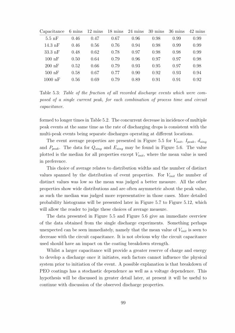
Capacitance 6 mins 12 mins 18 mins 24 mins 30 mins 36 mins 42 mins
5.5 nF 0.46 0.47 0.67 0.96 0.98 0.99 0.99
14.3 nF 0.46 0.56 0.76 0.94 0.98 0.99 0.99
33.3 nF 0.48 0.62 0.78 0.97 0.98 0.98 0.99
100 nF 0.50 0.64 0.79 0.96 0.97 0.97 0.98
200 nF 0.52 0.66 0.79 0.93 0.95 0.97 0.98
500 nF 0.58 0.67 0.77 0.90 0.92 0.93 0.94
1000 nF 0.56 0.69 0.79 0.89 0.91 0.91 0.92
Table 5.3: Table of the fraction of all recorded discharge events which were com-
posed of a single current peak, for each combination of process time and circuit
capacitance.
formed to longer times in Table 5.2. The concurrent decrease in incidence of multiple
peak events at the same time as the rate of discharging drops is consistent with the
multi-peak events being separate discharges operating at different locations.
The event average properties are presented in Figure 5.5 for Vinit, Ipeak, dsing
and Ppeak. The data for Qsing and Esing may be found in Figure 5.6. The value
plotted is the median for all properties except Vinit, where the mean value is used
in preference.
This choice of average relates to distribution widths and the number of distinct
values spanned by the distribution of event properties. For Vinit the number of
distinct values was low so the mean was judged a better measure. All the other
properties show wide distributions and are often asymmetric about the peak value,
as such the median was judged more representative in those cases. More detailed
probability histograms will be presented later in Figure 5.7 to Figure 5.12, which
will allow the reader to judge these choices of average measure.
The data presented in Figure 5.5 and Figure 5.6 give an immediate overview
of the data obtained from the single discharge experiments. Something perhaps
unexpected can be seen immediately, namely that the mean value of Vinit is seen to
decrease with the circuit capacitance. It is not obvious why the circuit capacitance
used should have an impact on the coating breakdown strength.
Whilst a larger capacitance will provide a greater reserve of charge and energy
to develop a discharge once it initiates, such factors cannot influence the physical
system prior to initiation of the event. A possible explanation is that breakdown of
PEO coatings has a stochastic dependence as well as a voltage dependence. This
hypothesis will be discussed in greater detail later, at present it will be useful to
continue with discussion of the observed discharge properties.
99

Capacitance / nF
Tim
e o
f pro
cessin
g /
min
s
Mean initiation voltage / V
101
102
103
6
12
18
24
30
36
42
470
480
490
500
510
520
530
540
550
560
570
Capacitance / nF
Tim
e o
f pro
cessin
g /
min
s
Median discharge peak current / A
101
102
103
6
12
18
24
30
36
42
0.01
0.015
0.02
0.025
0.03
0.035
Capacitance / nF
Tim
e o
f pro
cessin
g /
min
s
Median discharge event duration / s
101
102
103
6
12
18
24
30
36
42
4.5
5
5.5
6
6.5
7
7.5
8
8.5
9
9.5x 10
-5
Capacitance / nF
Tim
e o
f pro
cessin
g /
min
s
Median event peak power / W
101
102
103
6
12
18
24
30
36
42
4
6
8
10
12
14
16
18
20
a) b)
c) d)
Figure 5.5: Panel (a) shows the mean values of Vinit for each combination of coating
processing time and circuit capacitance; (b) the median values of Ipeak; (c) the
median values of dsing and (d) the median values of Ppeak.
100

Capacitance / nF
Tim
e o
f pro
cessin
g /
min
s
Median charge transfer per event / C
101
102
103
6
12
18
24
30
36
42
0.5
1
1.5
2
x 10-6
Capacitance / nF
Tim
e o
f pro
cessin
g /
min
s
Median energy dissipation per event / J
101
102
103
6
12
18
24
30
36
42
2
4
6
8
10
12
x 10-4
a) b)
Figure 5.6: Panel (a) shows the median Qsing for each combination of processing
time and circuit capacitance tested. In panel (b) the values of median Esing are
plotted.
5.4 Discharge event probability histograms.
Whilst the average values of a particular event property are of interest, the distribu-
tions are poorly characterised by a single number. In this section histograms of the
discharge event properties will be presented, normalised by total number so that
the value of each bin range represents the probability of a discharge event property
taking a value in that range.
Comparisons will made to highlight the variation of the event property distri-
butions with processing time and with circuit capacitance. In each figure, panel
(a) will show variation with processing time for a fixed capacitance of 200 nF, and
panel (b) will display variations with circuit capacitance for a coating processed for
30 minutes.
When considered in conjunction with Figure 5.5 and Figure 5.6, the probability
histograms should allow the reader a clear overview of the properties of the discharge
events recorded in this experiment. Figure 5.7 shows probability histograms for Vinit
for selected combinations of capacitance and processing time; Figure 5.8 shows Ipeak
data; Figure 5.9 shows dsing data; Figure 5.10 shows Ppeak data; Figure 5.11 the Qsing
data and Figure 5.12 the histograms of Esing values.
The histograms show the same trends as the property averages. Circuit ca-
pacitance is seen to cause a decrease in the observed distribution of Vinit values,
especially for the thicker coatings. For a fixed circuit capacitance, Vinit distribu-
101

0
0.05
0.1
0.15
0.2
0.25
400 450 500 550 600 650
6 mins18mins30 mins42 mins
Pro
ab
abili
ty
Voltage / V
0
0.05
0.1
0.15
0.2
400 450 500 550 600 650
5.5 nF33.3 nF200 nF1000 nF
Pro
ba
bili
ty
Voltage / Va) b)
Figure 5.7: Probability histograms of Vinit values, using bin widths of 7.87 V. Panel
(a) shows variation with processing time for a fixed capacitance of 200 nF, panel
(b) shows variation with capacitance for a 30 minute coating.
0
0.005
0.01
0.015
0.02
0.025
0.03
0.035
0 0.01 0.02 0.03 0.04 0.05 0.06 0.07
6 mins18 mins30 mins42 mins
Pro
ba
bili
ty
Event peak current / A
0
0.01
0.02
0.03
0.04
0.05
0.06
0 0.01 0.02 0.03 0.04 0.05 0.06 0.07
5.5 nF33.3 nF200 nF1000 nF
Pro
ba
bili
ty
Event peak current / Aa) b)
Figure 5.8: Probability histograms of Ipeak values, bin width was variable and took
the values 0.25, 0.34, 0.56 and 0.68 mA for 6, 18, 30 and 42 minutes processing
respectively. Panel (a) shows variation with processing time for a fixed capacitance
of 200 nF, panel (b) shows variation with capacitance for a 30 minute coating.
102

0
0.01
0.02
0.03
0.04
0.05
0 50 100 150 200
6 mins18 mins30 mins42 mins
Pro
ba
bili
ty
Event duration / µs
0
0.05
0.1
0.15
0.2
0 50 100 150 200
5.5 nF33.3 nF200 nF1000 nF
Pro
ba
bili
ty
Event duration / µsa) b)
Figure 5.9: Probability histograms of dsing values, with bin width of 2 µs. Panel (a)
shows variation with processing time for a fixed capacitance of 200 nF, panel (b)
shows variation with capacitance for a 30 minute coating.
0
0.05
0.1
0.15
0.2
0.25
0 5 10 15 20 25 30 35 40
6 mins18 mins30 mins42 mins
Pro
ba
bili
ty
Peak event power / W
0
0.05
0.1
0.15
0.2
0.25
0 5 10 15 20 25 30 35 40
5.5 nF33.3 nF200 nF1000 nF
Pro
ba
bili
ty
Peak event power / Wa) b)
Figure 5.10: Probability histograms of Ppeak values, with bin width of 1.2 W. Panel
(a) shows variation with processing time for a fixed capacitance of 200 nF, panel
(b) shows variation with capacitance for a 30 minute coating.
103

0
0.02
0.04
0.06
0.08
0.1
0.12
0.14
0 1 2 3 4 5 6
6 mins18 mins30 mins42 mins
Pro
ba
bili
ty
Charge transferred / µC
0
0.02
0.04
0.06
0.08
0.1
0.12
0.14
0 1 2 3 4 5 6
5.5 nF33.3 nF200 nF1000 nF
Pro
ba
bili
ty
Charge transferred / µCa) b)
Figure 5.11: Probability histograms of Qsing values, with bin width of 50 nC. Panel
(a) shows variation with processing time for a fixed capacitance of 200 nF, panel
(b) shows variation with capacitance for a 30 minute coating.
0
0.02
0.04
0.06
0.08
0.1
0.12
0.14
0.16
0 0.5 1 1.5 2 2.5 3
6 mins18 mins30 mins42 mins
Pro
ba
bili
ty
Energy dissipation/ mJ
0
0.02
0.04
0.06
0.08
0.1
0.12
0.14
0 0.5 1 1.5 2 2.5 3
5.5 nF33.3 nF200 nF1000 nF
Pro
ba
bili
ty
Energy dissipation / mJa) b)
Figure 5.12: Probability histograms of Esing values, with bin width of 30 µJ . Panel
(a) shows variation with processing time for a fixed capacitance of 200 nF, panel
(b) shows variation with capacitance for a 30 minute coating.
104

tions rise with increased coating process time. The Ipeak and dsing distributions are
seen at first to increase with circuit capacitance, however beyond about 200 nF the
property distributions are seen to move back down to lower values. For fixed ca-
pacitance both Ipeak and dsing distributions showed sustained increases with coating
thickness. Other key parameters follow the trends set by peak current and duration.
Comparison with in-situ monitoring data (section 4.2) shows that the single dis-
charge data from this experiment do not give an accurate reflection of the properties
of discharge events observed during bulk PEO processing, at least when the raw
measurements are considered. It will be shown in chapter 6 that when two property
correlations are considered, such as variation of dsing with Ipeak, the correspondence
is good. Furthermore it will be shown that some information obtained from single
discharge testing, relating to the scaling behaviour of the discharge events, cannot
be obtained from in-situ monitoring as easily.
In order to get to that point, it is important to develop an understanding of why
the measured properties from single discharge experiments behave in the observed
fashion. The key to understanding the observed distributions lies in understanding
why an increased circuit capacitance causes a shift to lower Vinit values. It will then
be shown in chapter 6 that applied voltage is a key parameter for the development
of discharge events during PEO; not only in single discharge testing but in bulk
processing also.
5.5 Clustering behaviour of discharge events.
In order to understand the behaviour of the event initiating voltages, there is an-
other aspect of the discharge behaviour which requires discussion, specifically the
tendency of discharge events to occur in clusters or sequences. For reasons discussed
shortly in subsection 5.5.3, the author believes these clusters of discharge activity
to represent a series of discharge events at, or close to, the location of the primary
event in each cluster. An example of an extended segment of single discharge data
from a 42 minute coating with a 1000 nF circuit capacitance, in which two clusters
are evident, is presented in Figure 5.13.
This behaviour was also seen in the in-situ monitoring experiments for the plots
of cumulative charge transfer plotted in Figure 4.5 and Figure 4.6. The tendency
seen was for events on the small area to occur during periods of high activity,
separated by periods of little or no discharging.
105
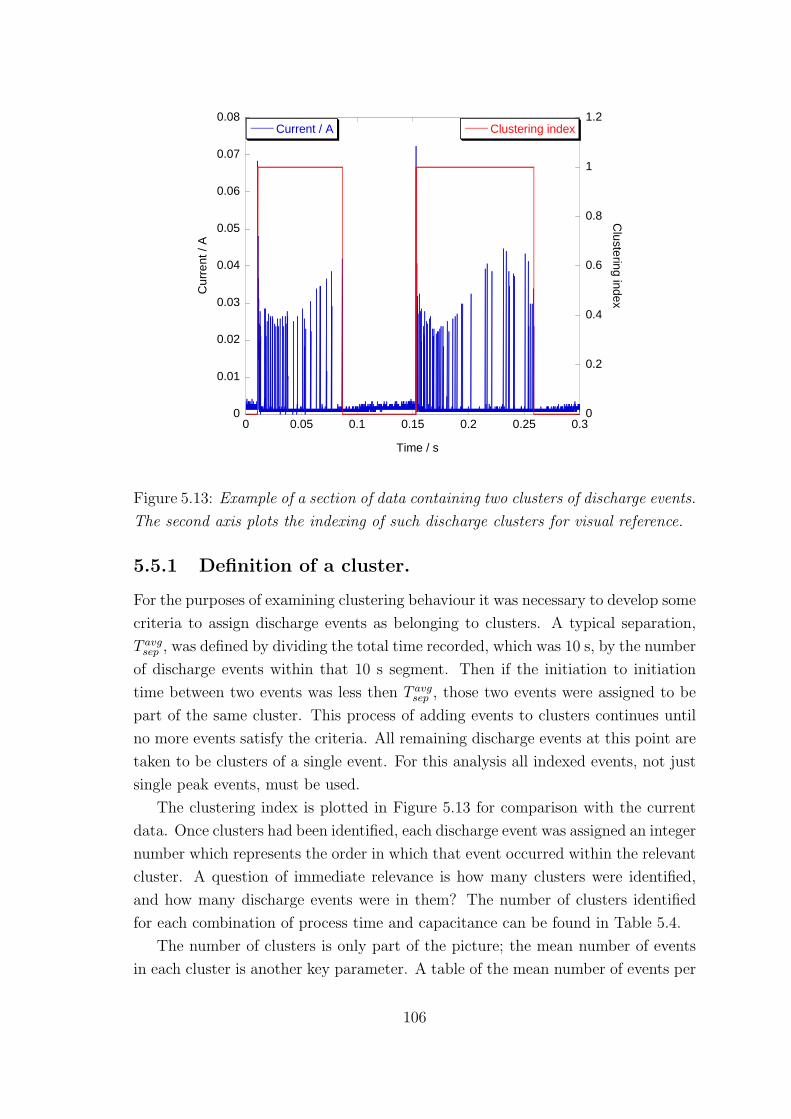
0
0.01
0.02
0.03
0.04
0.05
0.06
0.07
0.08
0
0.2
0.4
0.6
0.8
1
1.2
0 0.05 0.1 0.15 0.2 0.25 0.3
Current / A Clustering index
Cu
rre
nt / A
Clu
ste
ring in
de
x
Time / s
Figure 5.13: Example of a section of data containing two clusters of discharge events.
The second axis plots the indexing of such discharge clusters for visual reference.
5.5.1 Definition of a cluster.
For the purposes of examining clustering behaviour it was necessary to develop some
criteria to assign discharge events as belonging to clusters. A typical separation,
T avgsep , was defined by dividing the total time recorded, which was 10 s, by the number
of discharge events within that 10 s segment. Then if the initiation to initiation
time between two events was less then T avgsep , those two events were assigned to be
part of the same cluster. This process of adding events to clusters continues until
no more events satisfy the criteria. All remaining discharge events at this point are
taken to be clusters of a single event. For this analysis all indexed events, not just
single peak events, must be used.
The clustering index is plotted in Figure 5.13 for comparison with the current
data. Once clusters had been identified, each discharge event was assigned an integer
number which represents the order in which that event occurred within the relevant
cluster. A question of immediate relevance is how many clusters were identified,
and how many discharge events were in them? The number of clusters identified
for each combination of process time and capacitance can be found in Table 5.4.
The number of clusters is only part of the picture; the mean number of events
in each cluster is another key parameter. A table of the mean number of events per
106

Capacitance 6 mins 12 mins 18 mins 24 mins 30 mins 36 mins 42 mins
5.5 nF 137053 128579 99490 16948 6243 8035 5150
14.3 nF 103342 97505 59563 44979 5832 11243 3790
33.3 nF 80279 84096 60971 18067 9935 9418 4792
100 nF 56977 56929 57425 7402 15275 10993 9155
200 nF 40821 49180 40296 15733 14673 13550 6584
500 nF 23509 32219 33388 11288 11226 8183 6178
1000 nF 18165 23553 23791 10093 9636 5237 4711
Table 5.4: Table of the number of clusters of discharge events recorded for each
combination of capacitance and process time.
Capacitance 6 mins 12 mins 18 mins 24 mins 30 mins 36 mins 42 mins
5.5 nF 3.0 2.4 2.6 4.2 6.0 6.9 11.0
14.3 nF 3.0 2.6 2.8 3.5 6.9 5.4 7.6
33.3 nF 3.9 2.7 2.6 3.8 4.4 6.2 6.5
100 nF 4.4 3.1 2.6 4.6 3.7 4.2 3.9
200 nF 5.0 3.4 3.3 3.9 3.1 3.4 4.1
500 nF 7.1 4.0 3.7 5.4 5.0 5.2 5.7
1000 nF 8.6 4.9 3.8 5.8 6.2 6.6 7.5
Table 5.5: Table of the mean number of discharge events per cluster for each com-
bination of capacitance and process time.
cluster is presented in Table 5.5. It should be remembered this is only information
about clusters as they were defined earlier, ie according to a measure which is not
without problems.
Some measure of the clustering behaviour is required, however using the typical
separation Iavgsep is not always ideal. For example if all events occur roughly spaced
by a mean separation Iavgsep but with finite standard deviation, this will generate
a large number of spurious clusters of 2 or 3 members. However, as the number
of events added becomes larger, the likelihood of the cluster being the result of a
chance occurrence of discharges reduces considerably.
To try and account for such factors, a further measure of clustering may be
calculated as a bound on the clustering tendency of the discharge events. This was
taken to be the 90th percentile of numbers of event per cluster, after removal of
clusters containing less then 3 events. The results of this are displayed in Table 5.6.
The 90th percentile was chosen as a measure of upper bound on the clustering as it
is less sensitive to outliers then the maximum value.
107

Capacitance 6 mins 12 mins 18 mins 24 mins 30 mins 36 mins 42 mins
5.5 nF 8 8 10 25 32 30 47
14.3 nF 9 8 12 21 32 25 32
33.3 nF 10 8 10 27 33 41 26
100 nF 13 9 9 30 29 24 24
200 nF 14 11 13 23 27 17 21
500 nF 24 14 15 37 38 41 54
1000 nF 29 18 17 42 57 55 55
Table 5.6: Table of the 90th percentile of the number of discharge events per cluster,
after removal of clusters less than 3 in number, for each combination of capacitance
and process time.
5.5.2 The tendency towards clustering.
Taking Table 5.5 and Table 5.6 together, events appear to show a tendency towards
a greater probability of clustering for increases in the process time of the sample
coating. The same tendency is seen for increased circuit capacitance, though not
as strongly as for process times.
An increase with circuit capacitance makes sense, and might be expected given
that the applied voltage will decrease less over the course of an event with a larger
capacitance, as it will buffer the supply against the current loading of the discharge
more effectively. This will leave the voltage after termination of each event higher
than it would be for a smaller circuit capacitance, potentially increasing the prob-
ability of a subsequent breakdown event.
The estimated increase in the extent of clustering with coating process time may
be taken in the context of bulk PEO processing. Many authors have noted that
the discharge events have a tendency to become localised around certain sites as
processing proceeds, and generally appear by eye or by low speed optical imaging
to be longer lived and less mobile [2, 7, 8, 9, 16]. These empirical observations
are consistent with the information in Table 5.5 and Table 5.6.
Furthermore there does appear to be a transition in the upper bound of the dis-
charge numbers per cluster between 18 and 24 minutes. Whether the changes in dis-
charge event property distributions seen around similar process times in section 4.2
are related to such a step change in the likelihood of event clustering, possibly at a
localised site, is not possible to say absolutely from the present data. The timings
are compelling however, especially given the changes in the visual appearance and
colour of discharge events typical around 15-20 minutes into processing.
108

5.5.3 Likelihood of sequential events in clusters being
spatially related.
It is the authors opinion that these long clusters of discharge events represent suc-
cessive events occurring at or near to the location of the primary event in each
cluster. This is based primarily upon the observations of Vinit values of events dur-
ing clusters. A plot of the mean decrease in voltage between the primary event and
the initiation of the nth event in a cluster is shown in Figure 5.14 for data from the
1000 nF circuit capacitance.
It is seen that within each cluster, successive events occur at progressively lower
voltages. In one sense this is not surprising as the events occur in rapid succession,
and the capacitor cannot recharge much between termination of one and initiation
of the next. What is surprising is that the events keep initiating at voltages much
lower than that of the primary event. It should be remembered that prior to the
primary event the sample had been exposed to a higher voltage for a much longer
period, compared to the separation of events within the cluster.
This may be indicative of the first event somehow priming the discharge site and
allowing subsequent discharges at the same location to initiate at lower voltages.
This cannot be confirmed with the present dataset however. Whether such priming
is in the form of changes to the local structure of the coating, or whether it relates
to slight changes in the local composition of the electrolyte, or even persistence of
elevated temperatures at the discharge site is not possible to say.
It is worth referring back to the in-situ monitoring data, which showed discharg-
ing at later times in processing during periods of elevated activity spread across
multiple process cycles (see Figure 4.5 and Figure 4.6). Given the small area be-
ing monitored, such periods of activity probably correspond to discharges at, or
close to, a single location. The persistence across multiple process cycles at 50 Hz
is suggestive of a structural origin for the discharge clustering, as any thermal or
electrolyte effects would tend to be interrupted by the cycling of applied voltage.
Each event in such clusters is nevertheless associated with a distinct plasma, as
was confirmed by experiments in which a photo-multiplier module recorded concur-
rently with electrical monitoring, described in a previously published paper [1].
5.6 Relation of the initiating voltage and circuit
capacitance
Having established that the voltage tends to drop over the course of a cluster of
discharge events, and that clustering is favoured by thicker coatings and larger
109

0
20
40
60
80
100
120
0 20 40 60 80 100
6 mins18 mins
30 mins42 mins
Voltag
e d
ecre
ase fro
m p
rim
ary
even
t / V
Internal number of event
Figure 5.14: Mean decrease of applied voltage between initiation of primary event
in cluster and the nth event in the same cluster. Error bar is the standard error on
the mean.
110

460
480
500
520
540
560
580
600
620
640
10 100 1000
6 mins12 mins18 mins24 mins
30 mins36 mins42 mins
Me
an
initia
ting
vo
ltag
e in
clu
din
g a
ll e
ven
ts /
V
Capacitance / nF
460
480
500
520
540
560
580
600
620
640
10 100 1000
6 mins12 mins18 mins24 mins
30 mins36 mins42 mins
Me
an
initia
ting
vo
ltag
e o
f prim
ary
even
ts / V
Capacitance / nF
a) b)
Figure 5.15: Mean Vinit values taken from (a) all indexed discharge events (includ-
ing multi-peak) and (b) only those discharge events which were first in the respective
cluster. Errors on the mean values are too small to plot, distribution widths are sim-
ilar to those seen in Figure 5.7 and widths are not plotted for clarity of presentation.
capacitances, it is possible to ask whether the previously noted decrease in Vinit
with capacitance, seen in Figure 5.5 and Figure 5.7, is related to the clustering
behaviour. It is possible that the mean Vinit values were skewed by inclusion of data
from events at later stages of the discharge clusters, which become more sustained
with increased capacitance.
A comparison is presented in Figure 5.15 of the mean Vinit values for all indexed
discharge events (not just the single peak events) in panel (a), whilst panel (b)
shows the same information when only the primary event in a given cluster is
included. It can be seen that inclusion of more than the primary event does tend to
cause a lowering of the mean Vinit for discharges. However, the observed decrease
with capacitance remains, and furthermore is even more pronounced for the thinner
coatings than when all events were considered.
The question is now quite pressing as to why the circuit capacitance used should
affect the initiating voltages of discharge events. One of the physical parameters
which the capacitance can influence prior to onset of breakdown is the ramping rate
of the voltage. Larger capacitors do not just reduce the voltage decrease during an
event, the rate of recharging after event termination will also be reduced.
This point is illustrated by Figure 5.16. This figure plots for each 10 µs possible
separation period from the end of one cluster to the initiation of the next, the mean
111
Vinit which was observed. Only 10 µs separation periods for which there were at
least 10 values were included.
From Figure 5.16 it can be seen how the recharging rates varied with the circuit
capacitance. This confirms that, for example, a 12 minute coating which broke
down at 490 V with a 1000 nF circuit capacitance will have been exposed to that
voltage for a significantly longer period than a 12 minute coating through which a
discharge event was initiated at the same voltage using a 5.5 nF circuit capacitance.
It is the author’s feeling that the breakdown behaviour of PEO coatings displays
a significant stochastic component. Rather than there being a well defined break-
down strength for any given coating, the author would propose that there is instead
a probability of breakdown per unit time and area, which is a strong function of
the applied voltage and the existing coating structure. Therefore any given coating,
if exposed to a constant voltage, would show greater probability of breakdown the
longer the time for which it was exposed. For the present there is not sufficient data
to rigorously test such a hypothesis, though the experimental data from the single
discharge testing with different circuit capacitances does strongly suggest some form
of probabilistic dependence of the breakdown upon the applied voltage.
The consideration of event initiation is further complicated by the fact that one
may never cause electrical breakdown through the same PEO coating twice. The
nature of the process is that the local micro-structure is re-configured every time a
discharge occurs. Indeed if the discharges had no effect on the micro-structure the
growth of the coatings would never deviate from regular anodising.
High roughness and porosity levels also contribute to the uncertainty. The sur-
face connected nature of the porosity [6] means it is likely that electrolyte penetrates
into the interior of the coatings, much closer to the metal than the bulk thickness
would indicate. Even if this were not the case, the surface roughness would mean
that the precise field strength at any point on the surface would be highly variable.
Finally the roughness of the coatings and structural flaws in the coating (such as
the visible craters on the coating surface) mean that there will be no shortage of
sites at which electrical breakdown will occur more readily.
At the present stage, the data recorded has been insufficient to study the initi-
ation step of the discharges in detail. As such this text will not speculate as to the
precise nature of the physical processes which lead to the initial electrical breakdown
of the coating. Instead the discussion will consider in some detail the development
of discharge events after they have initiated. In chapter 6 it will be shown that once
the initial breakdown has occurred, the subsequent development of the discharge
event is heavily dependent upon the applied voltage. Once such relationships have
been understood, it will be possible to understand the trends observed with coating
112

440
460
480
500
520
540
560
0 500 1000 1500 2000 2500 3000
5.5 nF14.3 nF33.3 nF100 nF
200 nF500 nF1000 nF
Initia
tio
n v
oltag
e / V
Cluster separation / µs
Figure 5.16: Plot of the mean Vinit for each 10 µs period after termination of
previous event cluster. Only separation bins containing 10 initiated clusters were
included. This data corresponds to the 12 minute coating.
113

thickness and circuit capacitance for the Ipeak, dsing, Ppeak, Qsing and Esing values
measured from single discharge testing.
114

Chapter 6
Scaling Effects for Discharge
Events.
So far many measurements of the discharge properties have been presented, but
nothing has been presented to tie the measurements together into a more cohesive
framework. The hints of some underlying principles have already been seen, es-
pecially in the single discharge data. Examination of Figure 5.5 and Figure 5.6 is
suggestive of a link between the initiating voltage and the peak discharge current.
This will provide a starting point for this discussion of the scaling behaviour of PEO
plasma discharges.
6.1 Correlations between initiation voltage and
peak current in single discharge data.
Correlations between single peak discharge event Vinit and Ipeak were performed by
breaking down each dataset into subsets corresponding to a certain value of Vinit.
Recall that the voltage was recorded as 8-bit data over a range of ±1000 V, and the
minimum resolved voltage shift was 7.87 V. For each Vinit value a list was generated
of the Ipeak values of all events which initiated at that voltage. This list of current
values was then used to calculate every tenth percentile of the Ipeak distribution at
the specified Vinit. Only voltages at which a minimum of 100 events initiated were
included in such analyses.
The results of such calculation, for an 18 minute coating and a 200 nF circuit
capacitance are displayed in Figure 6.1. Once the effects of the spread in Vinit values
are accounted for in this fashion, the distribution of Ipeak values at each voltage is
found to be quite narrow and symmetric, in contrast to the distributions seen in
Figure 5.8.
115
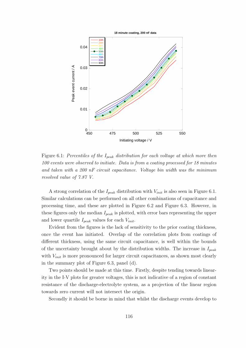
0
0.01
0.02
0.03
0.04
450 475 500 525 550
18 minute coating, 200 nF data
10th20th30th40th50th60th70th80th90th
Pea
k e
ve
nt
cu
rren
t /
A
Initiating voltage / V
Figure 6.1: Percentiles of the Ipeak distribution for each voltage at which more then
100 events were observed to initiate. Data is from a coating processed for 18 minutes
and taken with a 200 nF circuit capacitance. Voltage bin width was the minimum
resolved value of 7.87 V.
A strong correlation of the Ipeak distribution with Vinit is also seen in Figure 6.1.
Similar calculations can be performed on all other combinations of capacitance and
processing time, and these are plotted in Figure 6.2 and Figure 6.3. However, in
these figures only the median Ipeak is plotted, with error bars representing the upper
and lower quartile Ipeak values for each Vinit.
Evident from the figures is the lack of sensitivity to the prior coating thickness,
once the event has initiated. Overlap of the correlation plots from coatings of
different thickness, using the same circuit capacitance, is well within the bounds
of the uncertainty brought about by the distribution widths. The increase in Ipeak
with Vinit is more pronounced for larger circuit capacitances, as shown most clearly
in the summary plot of Figure 6.3, panel (d).
Two points should be made at this time. Firstly, despite tending towards linear-
ity in the I-V plots for greater voltages, this is not indicative of a region of constant
resistance of the discharge-electrolyte system, as a projection of the linear region
towards zero current will not intersect the origin.
Secondly it should be borne in mind that whilst the discharge events develop to
116
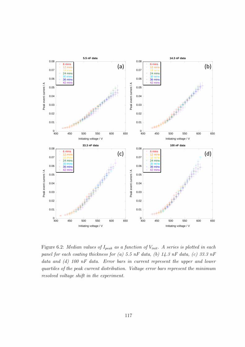
0
0.01
0.02
0.03
0.04
0.05
0.06
0.07
0.08
400 450 500 550 600 650
5.5 nF data
6 mins12 mins18 mins24 mins30 mins36 mins42 mins
Peak e
vent
cu
rrent /
A
Initiating voltage / V
0
0.01
0.02
0.03
0.04
0.05
0.06
0.07
0.08
400 450 500 550 600 650
14.3 nF data
6 mins12 mins18 mins24 mins30 mins36 mins42 mins
Peak e
vent
cu
rrent /
A
Initiating voltage / V
0
0.01
0.02
0.03
0.04
0.05
0.06
0.07
0.08
400 450 500 550 600 650
33.3 nF data
6 mins12 mins18 mins24 mins30 mins36 mins42 mins
Peak e
vent
cu
rrent /
A
Initiating voltage / V
0
0.01
0.02
0.03
0.04
0.05
0.06
0.07
0.08
400 450 500 550 600 650
100 nF data
6 mins12 mins18 mins24 mins30 mins36 mins42 mins
Peak e
vent
cu
rrent /
A
Initiating voltage / V
(a) (b)
(c) (d)
Figure 6.2: Median values of Ipeak as a function of Vinit. A series is plotted in each
panel for each coating thickness for (a) 5.5 nF data, (b) 14.3 nF data, (c) 33.3 nF
data and (d) 100 nF data. Error bars in current represent the upper and lower
quartiles of the peak current distribution. Voltage error bars represent the minimum
resolved voltage shift in the experiment.
117

0
0.01
0.02
0.03
0.04
0.05
0.06
0.07
0.08
400 450 500 550 600 650
200 nF data
6 mins12 mins18 mins24 mins30 mins36 mins42 mins
Peak e
vent
cu
rrent /
A
Initiating voltage / V
0
0.01
0.02
0.03
0.04
0.05
0.06
0.07
0.08
400 450 500 550 600 650
500 nF data
6 mins12 mins18 mins24 mins30 mins36 mins42 mins
Peak e
vent
cu
rrent /
A
Initiating voltage / V
0
0.01
0.02
0.03
0.04
0.05
0.06
0.07
0.08
400 450 500 550 600 650
1000 nF data
6 mins12 mins18 mins24 mins30 mins36 mins42 mins
Peak e
vent
cu
rrent /
A
Initiating voltage / V
0
0.01
0.02
0.03
0.04
0.05
0.06
0.07
0.08
400 450 500 550 600 650
Overall trends with capacitance
5.5 nF
14.3 nF
33.3 nF
100 nF
200 nF
500 nF
1000 nF
Peak e
vent
cu
rrent /
A
Initiating voltage / V
(a) (b)
(c) (d)
Figure 6.3: Median values of Ipeak as a function of Vinit. A series is plotted in
each panel for each coating thickness for (a) 200 nF data, (b) 500 nF data, (c)
1000 nF data and (d) overall data for all capacitances. Error bars in current rep-
resent the upper and lower quartiles of the peak current distribution. Voltage error
bars represent the minimum resolved voltage shift in the experiment.
118

the peak current without any strong influence of the existing coating thickness when
plotted against Vinit, this does not imply an independence of the discharges from
the prior coating structure. Remembering the discussion of the likely probabilistic
nature of breakdown event initiation, the probability of breakdown per unit time as
a function of applied voltage will depend upon the existing coating thickness and
structure. So in terms of the Ipeak value reached, the existing coating determines
the likely Vinit, and thereafter the applied voltage determines the subsequent event
development, up until the current peak is reached at any rate.
Such a dependence of Ipeak on Vinit might explain some of the literature results
relating to bulk current and voltage measures. Arrabal et al found for processing of
magnesium a significant 100 to 150 V decrease in applied voltage midway through
deposition of coatings [5]. According to the authors this coincided with a transition
of the processing to a ‘soft sparking regime’ with reduced apparent intensity of
discharge activity. This would be consistent with the finding of this work about the
dependence of discharge scale upon the applied voltage.
This does tend to lead into the question of why the Ipeak–Vinit relationship is
influenced by the circuit capacitance. It has been stated numerous times that the
purpose of the capacitance was to buffer the supply against the current loading of
the event, by providing a reserve of charge and energy. This is the reason that the
event development is influenced by the lower capacitances in particular.
As well as Vinit, the voltage at the point of peak current, Vpeak, was also measured,
as is outlined in subsection A.1.15. The difference between Vinit and Vpeak can give
an insight into the effects of increasing the circuit capacitance. Typical decreases
for the different circuit capacitances are shown in Figure 6.4.
The plot tells two things, firstly that decreases in applied voltage as the event
develops after initiation are probably responsible for the observed differences in rate
of Ipeak rise with Vinit. Secondly, the still reasonably large voltage decreases seen
with the 1000 nF capacitance would indicate that during bulk processing, when the
voltage will remain essentially constant over event lifetimes, greater Ipeak values still
should probably be expected for any given Vinit.
We are now in a position to understand the nature of the variation in the median
Ipeak values seen in Figure 5.5, panel (b). This can be explained using knowledge of
two factors, firstly that the distribution of Vinit values moves lower with increasing
capacitance, as discussed in section 5.6. Secondly the increase in slope of the Ipeak-
Vinit relationship with increased capacitance, caused by reductions in the voltage
drop as the events develop.
For the thinner coatings (6 and 12 minutes), the median Ipeak increases contin-
uously with circuit capacitance. This is as the decrease in Vinit with capacitance
119

0
10
20
30
40
50
60
70
80
400 450 500 550 600 650
5.5 nF14.3 nF33.3 nF100 nF200 nF500 nF1000 nF
Voltag
e d
rop fro
m initia
tio
n to p
eak /
V
Initiating voltage / V
Figure 6.4: Median differences between Vpeak and Vinit for the different circuit ca-
pacitances used, as a function of Vinit. Error bars represent the upper and lower
quartiles of the data at each Vinit value.
120

is low for the thin coatings, and the increased slope of the Ipeak-Vinit characteristic
dominates.
As the coatings thicken, the Vinit distributions are seen to be decreased more
significantly with increasing capacitance (Figure 5.5, panel (a)). The Ipeak values ob-
served initially increase with capacitance as the slope of the Ipeak–Vinit characteristic
increases. However, the rate of increase in the slope of the Ipeak–Vinit characteristic
slows with increasing capacitance, as seen in Figure 6.3 panel (d), and at larger
capacitances the shift to lower Vinit values is large enough that it is not compen-
sated for by the increased Ipeak-Vinit characteristic slope. This leads to the decrease
in observed median Ipeak for single discharge testing of thick coatings, for circuit
capacitances above about 200 nF.
6.2 Discharge event scaling and average current
development profiles for single discharge data.
During the computational methods discussion a procedure was outlined which allows
the calculation of average current development profiles of discharge events, for times
elapsed after initiation of the event, see section A.2. This analysis has so far been
neglected, however it allows for a more visual understanding of the scaling behaviour
of the discharge events.
Having established in the previous section that the Ipeak–Vinit characteristic is
insensitive to coating thickness, to within the achieved experimental resolution, data
used for calculation of average event development profiles will be averaged across
the seven different thicknesses used. Calculated profiles and associated uncertainties
are plotted in Figure 6.5 for the 1000 nF dataset.
With the exception of the smallest events, the shapes of the average discharge
profiles remain similar as Ipeak increases. A consequence of this is that dsing scales
in a similar fashion with voltage to Ipeak (at least the median does). The scale of
the uncertainty in the profiles is greatest around the peak current, though still of
small enough magnitude that the peak values for each initiating voltage may be
clearly differentiated.
The average profiles in Figure 6.5 are the average profiles for the median dsing
value at the relevant Vinit. The average profiles for events of differing duration,
within the subset of events for each Vinit, are also of interest. This information is
plotted in Figure 6.6. No systematic ordering of the different profile currents around
the peak location is seen with total duration, and the profiles plotted all lie within
about the standard error on the median dsing profile.
The development up to the peak shows little variation, and the gradient of the
121

0
0.01
0.02
0.03
0.04
0.05
0.06
0 50 100 150 200
Event profiles for 1000nF, all times
448.2 V456.7 V464.6 V472.4 V480.3 V488.2 V496.1 V503.9 V511.8 V519.7 V527.6 V535.4 V543.3 V551.2 V559.0 V566.9 V
Cu
rre
nt / A
Time after initiation / µs
Figure 6.5: Plot showing the averaged event development profiles for discharge events
at a range of Vinit. Profiles in each case are for the median dsing within the specified
Vinit subset. Error bars plotted are the standard error on a single current measure-
ment at that time after initiation of the event. Error bars are only plotted for every
other data series to avoid overcrowding the figure.
122

initial drop off after the peak appears similar in all cases. Much of the variation
between the different durations observed for a specific Vinit appears to be in the
precise point during the initial region of decreasing current at which the final rapid
drop off of current occurs.
The averaged voltage profiles were also calculated, however up until the point of
event termination, no variation was seen for events which initiated at the same volt-
age but which continued for different durations. This is understandable considering
the lack of significant deviations in the average current development profiles up until
the termination point. It does indicate that the differences in event duration are
probably not due to different behaviour of the applied voltage.
It is possible that the event termination is governed by the onset of some form
of instability in the plasma bubble as it expands into the fluid, though there is
insufficient data to test such a theory. What can be said reliably is that the event
development is dominated by the applied voltage up until the point where the
discharge current begins to drop rapidly.
6.3 Correlations between initiation voltage and
event duration in single discharge data.
Given the scaling of events in both current and duration, it follows that there will
also exist a correlation between Vinit and the event duration, dsing. The percentiles
of dsing at each Vinit value for all coating process times, and with the 1000 nF circuit
capacitance, are plotted in Figure 6.7.
The data in Figure 6.7 does show a strong correlation with voltage. The width
of the distribution is observed to be relatively large than that of Ipeak with Vinit,
especially towards the higher voltages (and hence larger events). This is likely a
consequence of the uncertainty in the timing of the final collapse of the discharge
current, as discussed with reference to Figure 6.6.
Having established that the discharge current signal scales in magnitude and
duration with the voltage applied, the other properties derived from these proper-
ties, such as peak power and charge and energy transfer, will of course also show
correlations with voltage. The other data presented in chapter 5 can therefore be
rationalised along similar lines to the Ipeak data.
As a final thought on the scaling of discharge events recorded during single
discharge testing, the correlation between Ipeak and dsing will be considered. The
percentiles of dsing observed for 1 mA binning of Ipeak values are plotted in Figure 6.8.
A good correlation is seen, and there is no doubt that there is a strong likelihood
of events which develop to greater Ipeak enduring longer. It should be noted though
123

0
0.01
0.02
0.03
0.04
0.05
0 50 100 150 200
Variation of events initiated at 551.2 V
median - 30 µsmedian - 20 µsmedian - 10 µsmedian durationmedian + 10 µsmedian + 20 µsmedian + 30 µs
Cu
rre
nt / A
Time after initiation / µs
Figure 6.6: Plot showing the averaged event development profiles for discharge events
at 551.2 V. Profiles are shown for the median dsing at this Vinit and also for events
within ±30 µs of the median. Error bars plotted are the standard error on a single
measurement of the current at that time after initiation of the event, the error has
only been plotted for the median duration profile.
124

0
50
100
150
200
250
300
440 460 480 500 520 540 560 580 600
10th20th30th40th50th60th70th80th90th
Event
dura
tio
n / µ
s
Initiating voltage / V
Figure 6.7: Plot showing every tenth percentile of the distribution of dsing at each
Vinit, for the 1000 nF circuit capacitance and including data from all coating thick-
nesses tested.
125

0
50
100
150
200
250
0 0.01 0.02 0.03 0.04 0.05 0.06
10th20th30th40th50th60th70th80th90th
Event
dura
tio
n / µ
s
Event peak current / A
Figure 6.8: Plot showing every tenth percentile of the distribution of dsing for 1 mA
binning of Ipeak values, for the 1000 nF circuit capacitance and including data from
all coating thicknesses tested.
that the data indicates a reasonable range of dsing at each Ipeak value, an indication
perhaps of the uncertainty in the exact point at which the discharge current finally
collapses.
6.4 Correspondence to in-situ monitoring data.
Having established a relationship of the event properties to the applied voltage for
single discharge experiments, we can now ask whether similar relationships hold for
discharges recorded as part of bulk processing experiments. The degree of corre-
spondence between the two datasets can also be assessed, as the scaling relations
allow for the difference in the electrical conditions applied to be compensated for
to a certain extent.
We shall begin by considering the correlation between Ipeak and dsing, plotted
in Figure 6.8 for single discharge data with a 1000 nF capacitance. The median
duration for each Ipeak value, using 1 mA binning, is plotted for each 150 s monitored
126
0
50
100
150
200
250
300
350
0 0.02 0.04 0.06 0.08 0.1 0.12 0.14
5 mins
7.5 mins
10 mins
12.5 mins
15 mins
17.5 mins
20 mins
22.5 mins
25 mins
27.5 mins
30 mins
32.5 mins
35 mins
37.5 mins
40 mins
Event
dura
tio
n / µ
s
Peak event current / A
Figure 6.9: Plot of the median dsing as a function of Ipeak for in-situ data. Error
bars plotted for the 20 minute data series were typical, and represent the distance
from the median to the upper and lower quartiles. Other error bars were not plotted
for clarity of the median positions.
period during in-situ experiments in Figure 6.9. The data for each time of processing
refers to the 150 s up to the specified time, and includes data obtained during the
specified time window.
There is a strong correlation evident in Figure 6.9 between Ipeak and dsing values.
The correlation is also seen to be minimally affected by the time of processing, as
was found for single discharge experiments. The largest deviation is seen for Ipeak
below about 40–50 mA, where the median dsing values for the data corresponding to
the first 15 minutes are seen to be slightly greater than for the data at subsequent
times. Referring back to chapter 4, there was a change in the observed distributions
of discharge properties between about 700 and 1000 s into processing. Whether the
split seen in Figure 6.9 is related to this is not presently clear, though it would be
tempting to make the association.
A comparison can be made between the in-situ data and the single discharge ex-
periment based around the Ipeak-dsing correlation. Only the data from the 1000 nF
127

experiments will be used, as this was the least impacted by the voltage decreases
inherent in the single discharge experiments. Data for all process times was con-
sidered together for both the single discharge and in-situ monitoring experiments.
The comparison can be found in Figure 6.10.
Good agreement is seen between the two datasets, despite the major differences
in electrical conditions used to generate them. The agreement is especially good for
events which exceeded Ipeak values above 30 mA. At lower Ipeak values the single
discharge data is found to lie at longer durations then the in-situ data. The exact
cause of this, and the significance, is not clear at present, though it may be related
to the different electrical conditions applied in each case.
In the single discharge experiments the voltage always decreased after initiation.
How this could lead to longer lived discharges is unclear. In the in-situ experiments,
any event was effectively in parallel with a large number of other active discharge
events (on the large unmonitored area). If more discharges ignited during the course
of an event, the additional pathways provided through the coating would tend to
reduce current flow to all other active events slightly. This might give rise to a
truncation of events in the in-situ monitoring experiment, and may explain the
observed differences in Figure 6.10. Such effects of competition between active
discharge events will be discussed further in section 6.5.
6.4.1 Correlations of initiating voltage and peak current
during in-situ monitoring.
The occurrence of each discharge event as part of a larger set of active discharges
during in-situ monitoring led to some significant deviations from the behaviour seen
for single discharge events. A similar plot to Figure 6.10 is plotted for the correlation
of Vinit and Ipeak in Figure 6.11.
Three things in particular are worth noting from the figure, firstly the median
Ipeak value from single discharge experiments is greater then the median Ipeak from
in-situ monitoring, especially at larger values of Vinit. Secondly the distributions of
Ipeak for each Vinit value are much wider for the in-situ data. Finally the lower end of
the Ipeak distribution shows no significant increase with Vinit for in-situ experiments.
The significance, or otherwise, of the slight downward shift of the distribution of
Ipeak values above 600 V is unclear. It is seen only for the 60th percentile and
lower, and is possibly indicative of a sharp rise in the number of simultaneously
active events at large voltage. With the depression of Ipeak values being due to the
discharge interaction effects discussed in section 6.5. Whether this is the case or
not, and whether the drop seen above 600 V is significant, is unclear at present.
Before discussing the possible reasons for the markedly different behaviour seen
128

0
50
100
150
200
250
300
350
400
0 0.02 0.04 0.06 0.08 0.1 0.12 0.14
Single discharge10th20th30th40th
50th60th70th80th90th
Event
dura
tio
n / µ
s
Event peak current / A
Figure 6.10: Plot of every 10th percentile of the dsing distribution against Ipeak with
1 mA binning, for the in-situ monitoring experiments. The median duration is plot-
ted for the single discharge experiments with 1000 nF capacitor, and the error bars
plotted represent upper and lower quartile of the dsing distribution for the 1000 nF
single discharge data within each Ipeak bin.
129
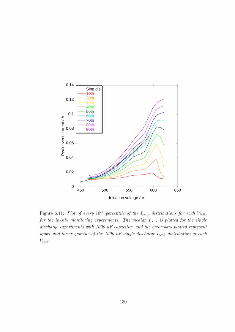
0
0.02
0.04
0.06
0.08
0.1
0.12
0.14
450 500 550 600 650
Sing dis10th20th30th40th50th60th70th80th90th
Peak e
vent
cu
rrent /
A
Initiation voltage / V
Figure 6.11: Plot of every 10th percentile of the Ipeak distributions for each Vinit,
for the in-situ monitoring experiments. The median Ipeak is plotted for the single
discharge experiments with 1000 nF capacitor, and the error bars plotted represent
upper and lower quartile of the 1000 nF single discharge Ipeak distribution at each
Vinit.
130

0
0.02
0.04
0.06
0.08
0.1
0.12
0.14
450 500 550 600 650
90th percentile 1000 nF90th percentile in-situ
Peak e
vent
cu
rrent /
A
Initiation voltage / V
Figure 6.12: Plot of the 90th percentile of Ipeak for each Vinit for both the single dis-
charge experiment with 1000 nF capacitance and the in-situ monitoring experiment.
during in-situ monitoring experiments, the reader should examine the data plotted
in Figure 6.12, which displays for both single discharge and in-situ datasets the
value of the 90th percentile of Ipeak at each value of Vinit. In this figure it can be
seen that whilst practically identical up to about 525 V, the upper end of the Ipeak
distribution for the in-situ data lies at higher current than the single discharge data
for further increases in Vinit.
The difference in the trend seen for distributions of Ipeak values with Vinit be-
tween the single discharge and in-situ monitoring experiments is due to competition
for current between concurrent discharge events in the bulk processing case. To help
understand this it will be useful to re-cap what was found for the Ipeak-Vinit rela-
tionships as the capacitance was increased.
From panel d) of Figure 6.3 it can be seen that the increase in Ipeak with Vinit
was more pronounced for larger capacitances. And it was then shown in Figure 6.4
that the decrease in voltage between the point of initiation and reaching peak cur-
rent increased for decreases in circuit capacitance. This establishes that decreases
in voltage over the initial period of the event development reduce the value of Ipeak
131

reached. For the in-situ monitoring data, in which the voltage did not vary signif-
icantly between initiation and the peak in discharge current, it would be expected
that Ipeak values at a given Vinit would be greater than for even the 1000 nF dataset
from single discharge experiments. This is as moderate decreases in applied voltage,
up to ∼ 30 V, were seen for the 1000 nF dataset between event initiation and peak
discharge current.
If we consider just the 90th percentile of Ipeak data at each Vinit, which may be
considered as an upper bound on the discharge current achievable at a given value
of Vinit, as in Figure 6.12, the expected trend is observed. This indicates that the
maximum Ipeak that can be reached by discharge events is determined by the applied
voltage in both experiments. The enhancement of the 90th percentile of the in-situ
data with respect to the 1000 nF data seen in Figure 6.12 is due to the absence of
a voltage decrease after event initiation in the in-situ case. The deviation becomes
larger as Vinit increases, as the decrease from Vinit to Vpeak for the 1000 nF single
discharge data also becomes larger for greater Vinit, as seen in Figure 6.4.
Having established that both physical systems have applied voltage as an upper
bound on Ipeak, the question remains as to why the distributions of Ipeak with Vinit
are different within the context of bulk PEO processing. Two simplified models
of discharge event interactions can aid this discussion. Both are simplistic, and
neither represents an especially close analogy to the reality, as the actual interaction
is likely closer to a mixture of the two viewpoints. On a basic level, the difference
seen between single discharge and in-situ datasets arises because in the former the
voltage is applied across a single event, whereas for the latter the voltage is applied
in parallel across many discharge events.
6.5 Discharge event interactions during bulk PEO
processing.
The first model considers a network of resistors connected in parallel. For a network
of N resistors, each of an unspecified resistance Rj, with an imposed current of IT ,
the current through each resistor will be given by the expression in Equation 6.1,
with RT the total resistance of the network. Examination of the current records
throughout the preceding text of this work will show that the effective resistance of
discharge events decreases from the initiation point to the peak current. Consider
next a discharge event which initiates at a point in time when several other discharge
events are already active across the sample surface. Assume further that the already
active discharges were initiated before the new event, and have already reached a
132

stage of development at which they present a significantly less resistive path.
Ij =RT ITRj
(6.1)
To put some numbers on this, the median resistance at the peak for an event
from single discharge testing with 1000 nF capacitance, initiated at 574.8 V, was
∼ 9500 Ω. By contrast, at the early stages of a discharge event the dynamic resis-
tance of the discharge is of the order several times 105 Ω. It can be seen then that if
another discharge event initiates whilst several, more developed, events are active,
it will impact the total resistance, RT , negligibly. The current drawn by the new
event will also represent a small fraction of the total by Equation 6.1. This will
reduce dramatically the energy input to the new event, and the development of the
discharge will likely be curtailed with respect to an event initiated in isolation.
So whilst the maximum Ipeak may be bounded by the applied voltage, the pres-
ence of concurrently active events across the sample surface will lead to a reduction
in the power supplied to any subsequently initiated discharge events. The degree
to which events are curtailed will be determined by the number and state of devel-
opment of the already active discharge events. This sort of competition between
discharge events could explain why the distribution of Ipeak with Vinit is so different
between single discharge and in-situ experiments.
There are not usually multiple events active on the small monitored area, how-
ever it is being processed in parallel with an area ∼ 100 times larger, and so there
will be a large number of discharge events active on the unmonitored areas of the
sample. By contrast an event initiated during single discharge testing has (more
often than not) no competition from other events, which may be why a much tighter
correlation is seen for Ipeak and Vinit.
That is one way to view the discharge interactions, but likely not the whole
story and alternative views should be considered. Whilst the resistance of the actual
discharge filaments is probably not large, the total contribution from the electrolyte
when the current flows locally to a small area (the discharge plasma bubble) could
be large. If the plasma bubble is assumed to be a perfect hemisphere, of radius rP ,
on the surface of the coating. And if it is assumed that the counter-electrode is
sufficiently distant and large that the current flow to the bubble may be considered
to be perfectly radial, then the total resistance from the surface of the bubble to
infinity is given by Equation 6.2.
R =ρ
2πrP(6.2)
133

The total potential difference between the bubble radius, rP , and general radius
r can be derived for specified discharge current I as in Equation 6.3.
∆V =Iρ
2π
(1
rP− 1
r
)(6.3)
The diameters of discharge events from Matykina et al [8] and Yerokhin et al
[2, 7] were of the order of several hundred µm. For the purposes of an estimate,
assume a value of rP = 100 µm, and take the discharge current to be 50 mA. The
conductivity of the electrolyte used was measured to be 5.1± 0.1 mS.cm−1, giving
for the resistivity a value of ρ ≈ 2 Ω.m. If we then use these values to estimate
the potential drop between the plasma bubble surface and a radius 1 mm from the
discharge site, the value obtained is δV ≈ 143 V.
This is likely a serious overestimate, and the assumption of radial symmetry
of the current to the plasma bubble is clearly inaccurate. The discussion does
demonstrate that current flow to active discharges could influence the development
of other events by reducing the effective potential difference at other regions of the
coating. If breakdown did occur some distance from the active event, it would be
at an effective voltage below the bulk applied potential, and would develop to lower
current accordingly. Such effects cannot be distinguished in the in-situ data, as only
the overall voltage could be measured.
Neither of these two examples is sophisticated enough to provide a sensible model
for the circuit interactions of discharge events during PEO processing. The examples
serve simply to illustrate some basic physical reasons why the distributions of Ipeak as
a function of Vinit display such a wide spread, as is seen in Figure 6.11. The measured
voltage between substrate and counter-electrode does not represent the absolute
value of voltage driving individual events observed during in-situ monitoring, it can
only tell the maximum driving force available to develop each event.
The exact reason why the voltage should determine an upper bound on the
discharge current is not clear, however the applied voltage does establish an energy
scale for the event, and the development of discharge events is likely to be linked to
the energy that can be supplied by the external circuit. In this regard it is perhaps
not surprising to find discharge event scale to be bounded by applied voltage.
6.6 Averaged profiles of discharge events recorded
during in-situ monitoring experiments.
The averaged profiles for a selection of different possible event durations of dis-
charges initiated at 559 V, during in-situ monitoring experiments, is presented in
134

Figure 6.13. The difference when compared to Figure 6.6 is pronounced. This gives
an indication of the impact of competition with other active discharge events on
the development of discharge events.
The event profiles have relatively larger standard error on a single current mea-
surement then for the single discharge data. Scaling of the discharge event shape is
also seen, reminiscent of Figure 6.5 for differing initiating voltages. Scaling of the
peak current only continues up to an upper bound determined by the voltage, at
which point event average profiles get no higher, only longer. This is seen in the
longest average profiles plotted in Figure 6.13.
Similarity of the scaling behaviour below the upper bound of peak current to
variations seen with applied voltage in single discharge experiments, is supportive of
the view that the effective voltage driving any given event development is variable,
and determined by the number and state of development of other discharge events
active at unmonitored sites elsewhere on the substrate surface.
6.7 Estimation of discharge event physical scale.
The values of the discharge resistance at peak current, Rpeak, were plotted in Fig-
ure 5.4 previously. The trends of Rpeak with Ipeak are re-plotted in Figure 6.14,
though in this case each series represents data from all coatings for a specific value
of the circuit capacitance. This data shows the same trend as was observed in
Figure 5.4, and confirms that Rpeak as a function of Ipeak was not sensitive to the
capacitance used during testing. Only data from the single discharge testing can be
used for this purpose, this is due to the effects discussed in section 6.5. The resis-
tance due to a single event, and the current flow to the event, cannot be determined
for the in-situ experimental data, in which the voltage is applied in parallel across
multiple active events at the same time.
A simple model already briefly discussed in section 6.5 can be applied to produce
a crude estimate of the physical size of discharge events. Recall Equation 6.2 for
the resistance for radial current flow to a hemispherical bubble. If it is assumed
that at the point of peak current the conductivity of the plasma is much larger than
that of the electrolyte, Equation 6.2 can be used to estimate a radius for the plasma
bubble, using the Rpeak values and the measured resistivity of the electrolyte used,
ρ ≈ 2 Ω.m. Results of such calculations are presented in Figure 6.15.
The assumption of much greater conductivity for the plasma may be considered
in terms of reported conductivity values for partially ionised plasmas. Data from
experiments on partially ionised caesium by Roehling [50], indicated σ ≈ 1 S.cm−1
for a temperature of ∼ 1800 K, falling rapidly as the temperature dropped, but not
135

0
0.01
0.02
0.03
0.04
0.05
0.06
0 50 100 150 200 250
Selected event profiles at 559 V
Event
curr
ent
/ A
Time / µs
Figure 6.13: Plot showing the averaged event development profiles for discharge
events at 559 V, taken from in-situ monitoring data. A series of the observed event
durations is plotted, and error bars plotted for selected series represent the standard
error on a single measurement of current at the relevant time after initiation of an
event with the respective duration. Not all error bars were plotted for clarity of the
figure, those plotted are representative of the trends observed.
136

103
104
105
106
0 0.01 0.02 0.03 0.04 0.05 0.06 0.07
5.5 nF14.3 nF33.3 nF100 nF200 nF500 nF1000 nF
Re
sis
tance a
t pea
k c
urr
ent /
ohm
s
Peak event current / A
Figure 6.14: Dynamic resistance of discharge events at the point of peak current,
Rpeak, as a function of Ipeak, with bin width of 676 µA. The width of the distribution
of Rpeak values at each Ipeak value was found to be too small to be resolved if plotted
on the figure.
137

0
5
10
15
20
25
30
35
40
0 0.01 0.02 0.03 0.04 0.05 0.06 0.07
5.5 nF14.3 nF33.3 nF100 nF200 nF500 nF1000 nF
Pla
sm
a r
ad
ius / µ
m
Peak event current / A
Figure 6.15: Estimated radius of the plasma bubble, rP , at the point of peak current
as a function of discharge peak current, Ipeak, with bin width of 676 µA.
138

equal to the electrolyte conductivity of 5.1± 0.1 mS.cm−1 until a temperature of
∼ 1300 K.
Kim and Kim calculated the conductivity of non-ideal aluminium [51] and non-
ideal iron and nickel plasmas [52]. The lowest temperature for which they report
values is 10 000 K for aluminium and 14 000 K for iron and nickel. For all three
metals the authors report minimum conductivities of > 10 S.cm−1, at least a thou-
sand time greater then the electrolyte conductivity. The temperatures reported for
PEO plasmas ranged from 3000 to 16 000 K [1, 14, 15], so the plasma conductivity
has potential to be significantly greater than that of the electrolyte for at least part
of the development of discharge events.
The values of radius estimated in Figure 6.15 are unlikely to be especially ac-
curate, however they compare well with the reported scales of discharge plasmas
reported in previous literature studies. Work by Matykina et al [8] and Yerokhin
et al [2, 7], found the discharge diameter to be in the range of a few hundred
µm (see subsection 2.1.4 for more discussion of literature values). The values of
plasma radius estimated in Figure 6.15 are below these values, however these would
represent the discharge scale at the peak current value. This occurs at a compar-
atively early stage of discharge development, no more than a quarter to a third
of the way through many events (see Figure 6.5), and so discharge events would
probably continue to expand beyond this point. The scale estimated in this fashion
is in good agreement with the scale of a few hundred µm obtained from analysis
of optical images. With more information about plasma electron temperature and
density, potentially obtainable from time resolved spectroscopy of discharge events,
the measured current signals could be used to develop a more physically realistic
model of the discharge plasma. Such an undertaking is beyond what is possible
with the information presently available.
139
Chapter 7
Conclusions
7.1 Characteristics of discharges.
The measured discharge characteristics presented in chapter 4, chapter 5 and chap-
ter 6 are specific to the combination of substrate, power supply and electrolyte used
in the present study. Without similar detailed information from another system it is
not possible to say to what extent the present data may be taken as representative
of wider PEO processing. Whilst the specific details will not be the same in other
PEO systems, the general features observed and the scaling relationships obtained
can allow some broad conclusions about PEO systems to be reached.
• At all times during PEO processing the discharge events are initiated across
a range of voltages; no evidence was seen of a well defined breakdown voltage
for discharging behaviour, even for a fixed coating thickness.
• Discharges occur across a range of scales in current, duration, power, energy
dissipated and charge transferred, at all points during coating deposition.
• Current-time plots of PEO discharges display self-similar scaling between
events which reached different peak discharge currents. This means that cor-
relations are seen between peak current and total duration, and probably also
physical size. The precise scaling of the typical discharge durations with the
discharge peak current probably varies between processing systems, but the
existence of such scaling behaviour would be expected for all PEO systems.
• The maximum scale of a PEO discharge event, in terms of electrical char-
acteristics, is bounded by the applied voltage. The precise details of the
relationship, for example the gradient of the correlation, would be assumed
to be different for different substrates, electrolytes, or power supply systems,
140

but a limit on the maximum scale of the discharge events with voltage will
probably apply to all systems.
• The initiation step of PEO discharge events has not been well resolved in the
present work. Evidence is presented which is consistent with a probabilistic
dependence of breakdown upon applied voltage. This manifested as a sensi-
tivity of measured coating breakdown voltages to the rate of voltage increase
during single discharge testing. Whilst the exact mechanism which leads to
this behaviour cannot be determined from the present dataset, it is probable
that similar behaviour would be observed for other PEO systems.
• The high degree of variability seen in the discharge characteristics demon-
strates that large numbers of measurements are required in order to develop
a reliable picture of discharge event behaviour in any given PEO processing
system.
• No clear separation of the discharge events into different types, eg sparks,
micro-arcs, arcs etc, was evident in the discharge characteristic measurements,
or in the averaged current development profiles. The discharge events recorded
formed a continuous range from small to large scale events, and the similar
current development profiles at different event scales indicate strongly that the
same physical factors are involved in the development of all discharge events.
Such distinctions between different ‘regimes’ of discharge types should not be
applied to the PEO process.
• The apparently longer lifetimes of discharges at longer processing times, when
observed by eye or low speed optical imaging, is most probably the result of
increased clustering and greater persistence of PEO discharges at, or close to,
the same spatial location.
7.2 Effectiveness of the techniques presented
The two experimental methodologies presented for the quantitative investigation
of PEO discharge events have been shown to allow measurement or calculation of
many useful characteristics of discharge events.
• The ‘in-situ monitoring’ technique allows for the measurement of discharge
event characteristics representative of PEO processing in the system under
investigation. In the present work the majority of data obtained did not allow
events smaller then 10 mA to be resolved. However, it was also shown that
such a limit was not inherent to the procedure.
141

• The ‘single discharge’ technique allows for the study of discharge event be-
haviour in the absence of interactions with concurrently active discharge events
elsewhere on the substrate. In particular this allows the relationship between
event development and applied voltage to be studied. Such studies cannot be
performed for the in-situ experiments as the precise electrical environment in
which a recorded discharge occurs cannot be determined in the in-situ testing.
• The single discharge testing does not allow event characteristics representative
of the bulk processing to be obtained, though event characteristic correlations
between peak discharge current and event duration compare well with those
obtained from in-situ experiments with the same electrolyte. Averaged current
development profiles were also seen to present a close match to the in-situ
dataset.
• Both methods presented in this work allow high data acquisition rates, and
are easily adapted to facilitate multiple, rapid, repeats. This is a requirement
for studying PEO discharges in any experimental system due to the high
variability possible between any given discharge event and the next event to
occur.
• Application to other PEO coating systems would require changes to be made
to some of the experimental parameters. Mostly this would be superficial
things such as the sizes of resistances and relative areas of samples. Slight
adjustments to the computing procedures would probably also be required for
the study of some alternative PEO processing systems.
7.3 Further work
There exists significant potential for further work, most importantly the applica-
tion of the quantitative measurement techniques presented in this work to other
systems of electrolyte, substrate and power supply. Such investigations will allow
understanding to be developed of the connections between discharging behaviour
and coating structure. The dependence of discharging behaviour upon the elec-
trolyte composition and concentration could be studied. Studies of systems known
to result in different phase compositions of coatings could be made, so that the
hypothesis of a link between discharge event thermal heating intensity and relative
phase proportions can be tested.
Development of a methodology to allow the probability of coating breakdown
as a function of applied voltage to be reliably measured should be a priority of any
142

further work. Understanding the initiation step of the discharge events is a key
aspect of discharge behaviour which was not well resolved in the present work.
143

Appendix A
Data analysis procedures for
single discharge experiments
A.1 Single discharge data processing.
The processing of information recorded from single discharge testing will be de-
scribed in this appendix. Algorithms for each task will be presented and described,
and the operation of each upon a representative section of data illustrated with
figures where appropriate. The example section was taken from testing of an 18
minute coating using a 200 nF capacitor, and the value of the current measurement
resistor was 464 Ω. Calculations were performed using Matlab 7, and algorithms
were written in the scripting language of that package. Pseudo-code will be used in
preference to source code in this discussion for purposes of clarity.
A.1.1 Scaling of variables and calculation of the baseline
current level.
The first procedure is to scale the raw data so that current and voltage data are
in (S.I.) units. The data for voltage and current was in the form of vector arrays,
with 10 million entries each. The current data was in the form of the voltage across
the probe resistor, of magnitude R Ω, which was recorded using a 1× attenuation
probe. The voltage data was recorded using a 100× attenuation probe.
The vector containing the voltage data was called A, and the vector containing
the current B. The scaling used was as detailed in Equation A.1, in which the
144

subscript j refers to the jth element of the relevant vector array.
Vj = Aj × 100 ∀ j
Ij =−Bj
R∀ j
(A.1)
The minimum resolvable current step was determined according to Equation A.2.
This results from the resistance, R, having been set to generate a signal from the
current in the range 0 to 20 V. The factor of 127 results from the 8-bit digitisation
of the data by the oscilloscope. Istep represents the minimum resolvable shift in
the current signal. For the data section which will provide illustrative examples,
Istep = 340 µA.
Istep =20/R
127(A.2)
A sample of the correctly scaled current and voltage data is presented in Fig-
ure A.1. The form of the signal is of a low baseline current interrupted by discrete
current peaks. These current peaks correspond to discharge events, and the cor-
respondence of such current peaks to optical emission was previously established
in a published article [1]. The voltage can also be seen to decrease slightly over
the duration of the current peaks due to overloading of the power supply by the
discharge event.
In the figure there is one event which appears as a superposition of two current
peaks. Whether this represents a single event, or two separate events overlapping
in time, is not resolvable from this data alone. Such event will not be discounted
from consideration, but identification is required in order that later analyses can be
restricted to single peak events if desired.
The approximate level of the baseline current seen in Figure A.1 is important
for subsequent stages of processing. This was defined as the variable Ibase. A
histogram of all current values, with bins centred around integer multiples of Istep,
was calculated; the most common value was assigned to be Ibase. The distribution
was sharply peaked, as can be seen in Figure A.2, which relates to the entire 10 s
data segment from which the section in Figure A.1 was taken. It can be seen from
this that Ibase = 680 ± 340 µA for this particular data section. It is worth noting
that the baseline level is approximate, and calculated globally for a data segment
of 10 million entries. In the example shown in Figure A.1 the baseline is running
about 1× Istep above this level.
145

0
0.005
0.01
0.015
0.02
0.025
0.03
0
100
200
300
400
500
600
0 200 400 600 800
Current / A Voltage / V
Cu
rre
nt / A
Volta
ge
/ V
Time / µs
Figure A.1: Sample of the correctly scaled current and voltage data from single dis-
charge experiments. Data from an 18 minute coating tested with a 200 nF capacitor.
101
102
103
104
105
106
107
0 0.01 0.02 0.03 0.04
Frequency
Fre
quency
Current / A
Figure A.2: Histogram of all current values in one 10 s data record. The most
common value is assigned to be Ibase.
146

A.1.2 Calculation of a gradient measure.
A measure of the gradient of the current data was required. The measure used was
the 4th order finite difference gradient, as defined for a function f(t) by Equation A.3.
df
dt=
2
3δt
[f(t+ δt)− f(t− δt)− 1
8(f(t+ 2δt)− f(t− 2δt))
]+O(δt4)
then if F is a vector such that
Fj = f(j × δt)can write a measure of the gradient at the jth entry as
dFj =2
3δt
[Fj+1 − Fj−1 −
1
8(Fj+2 − Fj−2)
](A.3)
The gradient measure of the current data was calculated according to the proce-
dure outlined in Algorithm 1. The first part of this procedure generates the gradient
measure. The time step duration δt was omitted as the gradient measure was scaled
to lie between -1 and 1 in the second part of the algorithm. This scaling of the gra-
dient was performed to allow easy graphing on the same y-axis as logical variables.
An example of the calculated current gradient measure dI is plotted in Figure A.3
for illustration.
Algorithm 1 Calculation of gradient measure.
N is total length of results vectors Ij and Vj
for j = 3 to N − 2 do
dIj ←2
3
(Ij+1 − Ij−1 −
1
8(Ij+2 − Ij−2)
)end for
assign dIscale ← maximum value of∣∣∣dIj∣∣∣
for all j do
dIj ←dIj
dIscaleend for
As can be seen from Figure A.3, the 8-bit nature of the data recorded by the
oscilloscope leads to large fluctuations in the current gradient measure dI. It is
only when the current is changing rapidly that the gradient measure is useful. The
dI vector will only be used for two purposes in the data processing as a result of
this. The first use will be to identify the approximate locations and current values of
stationary points (subsection A.1.3). The second use will be as part of the procedure
for indexing of the rising and falling edges of current peaks.
147

-0.04
-0.03
-0.02
-0.01
0
0.01
0.02
0.03
0.04
-0.4
-0.3
-0.2
-0.1
0
0.1
0.2
0.3
0.4
0 200 400 600 800
Current / A Current gradient measure
Cu
rre
nt / A
Cu
rren
t gra
die
nt m
ea
su
re
Time / µs
Figure A.3: The representative section of experimental data, showing current and
current gradient measure.
A.1.3 Listing of current signal stationary points.
A listing of stationary points as defined by a change in the sign of the gradient
measure, dI, was required. The procedure for compiling this list is detailed in
Algorithm 2. In this algorithm, N is the total length of the I and V array vectors
and list is an array of dimension Nstat row by 2 columns. The value Nstat is the
total number of stationary points identified by the conditions detailed in Algorithm
2. The first column lists the locations, j, of stationary points and the second the
corresponding current values Ij.
The algorithm passes through the current gradient measure, dI, and identifies
when the gradient measure changes sign. When this happens, it is determined
whether the implied zero is closer to dIj or dIj−1, and the appropriate values of index
coordinate and corresponding current value are copied into the listing variable, list.
A.1.4 Determination of the initial current threshold.
A histogram of the current levels corresponding to stationary values is first gener-
ated. Such a plot is shown in Figure A.4. The first, and larger, peak corresponds
to fluctuations around Ibase. The second, lower peak corresponds approximately to
the current peaks of discharge events.
The minima between the two peaks seen in Figure A.4 is found and set equal
148

Algorithm 2 Listing of stationary current values.m← 0
for j = 1 to N do
if dIj < 0 AND dIj−1 ≥ 0 then
m← m+ 1
x← dIj−1
dIj−1 − dIjif x > 0.5 then
listm,1 ← j
listm,2 ← Ij
else
listm,1 ← j − 1
listm,2 ← Ij−1
end if
else if dIj > 0 AND dIj−1 ≤ 0 then
m← m+ 1
x← dIj−1
dIj−1 − dIjif x > 0.5 then
listm,1 ← j
listm,2 ← Ij
else
listm,1 ← j − 1
listm,2 ← Ij−1
end if
else
do nothing
end if
end for
149

101
102
103
104
105
106
107
0 0.01 0.02 0.03 0.04
Frequency
Fre
quency
Current stationary point / A
Figure A.4: Histogram of stationary point values, frequency axis is logarithmic.
to a threshold value, Ithresh. A minimum shift in the current required to identify
a current peak, Ishift, is then defined on the basis of the values of Ithresh, Ibase and
Istep, according to Equation A.4.
Ishift = Ithresh − Ibaseif Ishift < 5× Istep then instead let
Ishift = 5× Istep
(A.4)
It is required that Ishift be at least 5 times the minimum resolvable current
shift, Ishift. This minimum is required in order to ensure reliable outcomes for the
processing algorithms which index the locations of discharge events. Ibase and Ishift
are approximate only, and represent best estimates to begin the indexing process.
A.1.5 Preliminary indexing of regions of interest.
Identification of the locations of discharge events in the data is easily done by eye,
but far too time consuming to make sufficient measurements manually. This next
section of the data processing begins the process of indexing and listing the periods
during which discharge events occurred.
The first step calculates an array vector, termed H, and the algorithm for this
150

is outlined in Algorithm 3. The algorithm starts with the variable sum set to zero.
At every time point in the current record the sum variable is either set equal to
zero if the current level is less then Ibase + Ishift, or if this threshold is exceeded
then sum is incremented by a quantity equal to the multiple of Istep by which Ij
exceeds Ibase. At each stage the present value of sum is set to be the value of Hj.
A comparison of the reference section of data with the calculated H variable is
presented in Figure A.5.
Algorithm 3 Procedure to calculate variable H.sum = 0
for j = 1 to N do
if Ij > Ibase + Ishift then
sum← sum+Ij − IbaseIstep
else
sum← 0
end if
Hj ← sum
end for
introduce G, a logical index array vector
for all i do
if Hj > 128 then
Gj = 1
end if
end for
for j = N to 2 do
if Gj = 1 AND Gj−1 = 0 AND Hj−1 > 0 then
Gj−1 ← 1
end if
end for
After calculation of the H variable, indexing is begun by assigning the value
1 or 0 to entries of the vector G, depending on whether that time point is inside,
or outside, a discharge event. This is initially done by assigning any point at
which Hj > 128 to be part of a discharge event. The procedure then backtracks
to the point at which Hj first exceeded 0, ie the point at which the threshold
value of Ibase + Ishift was first exceeded. The outcome of this overall procedure is
not displayed in another figure as it would provide no additional information over
151

0
0.005
0.01
0.015
0.02
0.025
0.03
0
1000
2000
3000
4000
5000
6000
7000
0 200 400 600 800
Current / A H indexing variable
Cu
rre
nt / A
H in
de
xin
g v
aria
ble
Time / µs
Figure A.5: The representative section of experimental data, showing current and
the indexing vector H.
Figure A.5.
This might seem an unnecessarily complicated procedure to get to this point.
Why not simply assign Gj = 1 at each point for which the current is above the
threshold value? This would certainly be effective on the section shown in Fig-
ure A.5. The procedure outlined in Algorithm 3 was adopted because it performs
better in certain situations, in particular with fluctuations in the recorded current
signal which can occur around the same time as the current is passing up or down
through the threshold value.
Using the H calculation procedure did not appreciably increase computation
time, and helped reduce the number of mis-indexed regions identified via manual
inspection. The chosen threshold of 128 means that an event which only exceeds
the threshold value by 1 × Istep would need to persist for a period in excess of
128× δt in order to be counted (δt = 1 µs for this work). A larger discharge would
not need to persist for as long to register. In particular the value of 128 means that
it is impossible for a spike which only lasted 1 sampling interval to register, as the
maximum value with the 8-bit oscilloscope vertical resolution is 127× Istep.
152
A.1.6 Extension of indexing to cover discharge event
initiation.
By this stage all significant current peaks have been partially indexed. However,
the point at which the current exceeds the threshold value is not the exact initiation
point of the event. The falling edge of the discharge events is similarly excluded
from the indexing at this stage.
The rising edge of the discharge event current peak can be included by con-
sideration of dI around the initiating point. Recalling Figure A.3, the gradient
measure was most accurate when the rate of change of current exceeded about
Istep/δt. Typically this is the case during the initial rise, and terminal fall, of the
discharge current. This allows the gradient measure dI to be useful when extending
the indexing to cover the rising edge of the discharge.
Algorithm 4 Procedure to extend the indexing to cover the discharge rising edge.
for j = N to 2 do
if Gj = 1 and Gj−1 = 0 and dIj−1 ≥ 0 then
Gj−1 ← 1
end if
end for
A procedure outlined in Algorithm 4 extends the discharge rising edge back in
time to the point at which the gradient measure exceeds zero. This works well in
most cases. However if there is a fluctuation on the rising edge of the discharge,
and if this fluctuation is just below Ibase + Ishift, then the rising edge below this
value may not be indexed. This was not a common problem however, the discharge
rising edge being about the most reproducible feature of the discharging behaviour,
as shown in chapter 6. The output of data analysis up to this point can be seen in
Figure A.6. It can be seen from the figure that the rising edge of the discharges is
now accurately covered by the indexing, the falling edge of the discharge remains
not indexed as yet.
A.1.7 Extension of falling edge to same current level as
initiation
The first stage of extending indexing to the falling edge of the discharge involves
extending the indexing to cover the discharge event until the current level has
returned to within Istep of the starting current. The procedure for this is detailed in
Algorithm 5. This works by scanning through the current record, and storing the
current when the start of an indexed region is encountered as Itemp. A logical flag
153

0
0.005
0.01
0.015
0.02
0.025
0.03
0
0.2
0.4
0.6
0.8
1
1.2
0 200 400 600 800
Current / A Logical index G
Cu
rre
nt / A
Lo
gic
al in
dex G
Time / µs
Figure A.6: The representative section of experimental data, showing current and
the logical indexing vector G.
is also set to indicate that the algorithm is now in a region of interest. When the
termination of the indexed region is reached, new points are added to the end until
the current level, Ij, drops to within Istep of Itemp.
This procedure was adopted as it is effective when dealing with two sub-classes
of event. Firstly of events which displayed a significant plateau region after the
initial peak, but before a rapid final drop back to the baseline current. Secondly
of events which had a two peak structure, with a minima just below the threshold
current level, but still greater then the baseline current. It was necessary for such
events to extend indexing in this manner prior to applying gradient conditions to
ensure appropriate bounds on regions of interest.
A.1.8 Extension of index to cover falling edge.
After extending the indexed regions until the termination current is within Istep of
the initiating current, the falling edge was further extended for those events which
still show negative current gradient at the termination of the index. This procedure
can be found in Algorithm 6, and is seen to be essentially similar to Algorithm 4.
The output of the indexing procedure at this point can be seen in Figure A.7.
The indexing stored in the logical variable G can now be seen to encompass the
discharge events in their entirety. The next task is to list the start and end points of
regions of interest, so that subsequent procedures need only examine those sections
154

Algorithm 5 Procedure to extend the falling edge until termination current is close
to initiating.Itemp ← 0
event← 0
for j = 2 to N do
if event = 0 then
if Gj = 1 AND Gj−1 = 0 then
event← 1
Itemp ← Ij
end if
else
if Gj = 0 AND Gj−1 = 1 then
if Ij − Itemp > Istep then
Gj ← 1
else
event← 0
end if
end if
end if
end for
Algorithm 6 Procedure to extend the falling edge whilst gradient is less then zero.
for j = 1 to N − 1 do
if Gj = 1 AND Gj+1 = 0 AND dIj−1 ≤ 0 then
Gj+1 ← 1
end if
end for
155

0
0.005
0.01
0.015
0.02
0.025
0.03
0
0.2
0.4
0.6
0.8
1
1.2
0 200 400 600 800
Current / A Logical index G
Cu
rre
nt / A
Lo
gic
al in
dex G
Time / µs
Figure A.7: The representative section of experimental data, showing current and
the logical indexing vector G.
of the data which are of relevance. Before doing so, there is one further small
procedure which is applied. Any points in the data for which Gj = 0 whilst Gj−1 = 1
and Gj+1 = 1 are set to be also equal to 1. This removes isolated points within
indexed regions, however, if the un-indexed point represents a genuine separation
of two events, then it will be later re-instated, subject to a locally derived current
threshold. This seems perhaps a little long winded, however the procedure overall
reduces the mis-identification of discharge events.
A.1.9 Listing of indexed regions.
The procedure for listing the coordinates of discharge initiation and termination
points is given in Algorithm 7. This involves passing through the data, incrementing
a running count whenever a discharge initiation is encountered, and listing the
starting and ending coordinates of the indexed regions in an array, index, with
dimension Nevent by 3. Nevent is the total number of indexed regions. The final row
of index is removed prior to determination of Nevent as quite often an event would
commence just before the end of the recorded region, but would not terminate before
the logging did. There are 3 columns in the variable index, the first is the event
start coordinates and the second the end coordinates. The third will not be used
until the internal peaks of indexed regions have been identified, and will represent
the total number of current peaks within each indexed region, see subsection A.1.14
156

for further details.
Algorithm 7 Procedure to list the starting and ending coordinates of indexed dis-
charge events.m← 0
for j = 2 to N do
if Gj = 1 AND Gj−1 = 0 then
m← m+ 1
indexm,1 ← j − 1
else if Gj = 0 AND Gj−1 = 1 then
indexm,2 ← j
else
do nothing
end if
end for
remove final row of the index variable
Nevent ← m− 1
A.1.10 Removal of events of insufficient magnitude.
A few additional procedures are required before the data can be passed to the algo-
rithm which will identify internal peaks and troughs. At the present stage of data
processing, for the dataset from which the example data section is drawn, repre-
senting a 10 s test period of an 18 minute coating with a 200 nF circuit capacitance,
the variable index contains 11640 rows, each corresponding to a discharge event.
Algorithm 8 Procedure to remove events below a threshold magnitude of 5Istep.
for j = 1 to Nevent do
Imax ← maximum Im in the range m = indexj,1 to indexj,2
Imin ← minimum Im in the range m = indexj,1 to indexj,2
if Imax − Imin < 5Istep then
for all indexj,1 ≥ m ≤ indexj,2 do
Gm ← 0
end for
end if
end for
In some of the datasets, some of the events identified up to this point will have
been incorrectly identified. So after the listing of indexed variables a subsequent
157
processing is applied to each of these regions. Any indexed discharge events which
do not show a base to peak current variation of at least 5Istep are removed from the
list, and the corresponding time points in the indexing variable G set equal to zero.
This procedure is outlined in Algorithm 8. Typically by this stage this condition
is not realised by more then a handful of the previously indexed events. For the
example dataset, the index variable still contains 11640 rows after application of
this condition.
A.1.11 Splitting of events which might be independent.
A routine is applied which causes a break in the indexing mid-way through any
region which could conceivably be two or more independent regions, previously
joined together either by a fluke of the prior conditions or explicitly when the
isolated points were removed during subsection A.1.8. The procedure for this is
presented in Algorithm 9.
Algorithm 9 Procedure to separate possibly independent indexed regions.
for j = 1 to Nevent do
k ← indexj,1
Itemp ← Ik
for m = indexj,1 to indexj,2 do
if Im ≤ Itemp + 1.1Istep then
Gm ← 0
end if
end for
end for
The stated condition of ≤ Itemp + 1.1Istep is to ensure that anything within Istep
of the initiating current level of the event, Itemp is indexed as not part of a discharge
event. The factor of 1.1 not 1 is to ensure that errors arising from rounding error
(Istep is stored only to finite precision) do not lead to a point remaining indexed
when it is equal to Itemp + Istep to within the measurement uncertainty, but not
exactly equal. As far as a computer is concerned, 1.000 6= 1.005, experimentally
they may be equivalent depending on the measurement uncertainty.
A.1.12 Finalising of indexing.
After the changes to the G logical index array in the previous subsections, the
discharge listing variable index must be updated. This is according to Algorithm
7 as before. After this the number of rows in the index variable for the example
158

dataset has increased from 11 640 to 13 673. Not all of these new regions are sensible
events however. A common problem results from slight fluctuations around the
termination point of the discharge events. The application of the condition detailed
in subsection A.1.11 can lead to such slight fluctuations, typically just after the
main current drop on event termination, being split off as a separate event.
To remove such artefacts, the condition on event magnitudes described in sub-
section A.1.10 is re-applied. This is followed by a final application of the listing
procedure of subsection A.1.9. After this, the final index variable for the example
dataset contains 12 397 rows, each representing a discharge event.
A.1.13 Indexing of internal peaks.
Whilst the intent of the single discharge testing was to generate discharge events
that were well separated and easily resolvable in time, the reality was not so simple.
Single peak current events did dominate all single discharge datasets, so the name
chosen is not completely spurious. However, multiple peak events, taking the form
usually of two or more of the single peak events superimposed on top of each other,
were often seen in the current records. It cannot be determined from the electrical
data alone whether such multiple current peak events represented single discharge
events showing significant fluctuation, or whether they represent concurrent opera-
tion of spatially distinct events. The latter possibility is more probable. In either
case it is important that single and multiple peak events be distinguished so they
can be treated separately during analysis of the discharge characteristics.
A procedure to identify whether indexed regions displayed significant internal
structuring was developed, detailed in Algorithm 10. The output of this procedure
is plotted for the by now familiar representative sample data in Figure A.8. The
precise mechanics of the algorithm may benefit from additional explanation.
Recall that dI suffered from large fluctuations due to the 8-bit nature of the
raw data (subsection A.1.4). This rendered it unusable except in regions where the
current was changing rapidly. Unfortunately, the gradient measure was not reliable
enough to be used for indexing of internal peaks within multiple peak discharge
events.
An alternative procedure was developed instead, that presented in Algorithm
10. At the start of the event, the algorithm is looking for a current peak. The
current peak magnitude, Ipeak, and location, kpeak, are set to the initiation current
of the event and the time coordinate respectively. For each subsequent time point
in the indexed region, if Im is greater than or equal to the currently stored Ipeak
value, then it is set to be the new Ipeak value. The peak location, kpeak, is also
updated to be m.
159

Algorithm 10 Procedure to identify locally significant peaks and troughs within
indexed regions.
F is another indexing vector array, similar to G and H.
for j = 1 to Nevent do
Imax ← maximum Im in the range m = indexj,1 to indexj,2
Imin ← minimum Im in the range m = indexj,1 to indexj,2
Iscale ← 0.2× (Imax − Imin)
kpeak ← indexj,1, ktrough ← indexj,1
Ipeak ← Ikpeak, Itrough ← Iktrough
seekpeak ← 1, seektrough ← 0
if Iscale < 5Istep then
Iscale ← 5Istep
end if
for m = indexj,1 to indexj,2 do
if seekpeak = 1 then
if Im ≥ Ipeak then
Ipeak ← Im
kpeak ← m
else if Im < Ipeak − Iscale then
Fkpeak← 1.0
seekpeak ← 0, seektrough ← 1
ktrough ← m
Itrough ← Im
end if
else if seektrough = 1 then
if Im ≤ Itrough then
Itrough ← Im
ktrough ← m
else if Im > Itrough + Iscale then
Fktrough← 0.5
seektrough ← 0, seekpeak ← 1
kpeak ← m
Ipeak ← Im
end if
end if
end for
end for
160

0
0.005
0.01
0.015
0.02
0.025
0.03
0.2
0.4
0.6
0.8
1
1.2
0 200 400 600 800
Current / A Logical index GInternal index F
Cu
rre
nt / A
Lo
gic
al in
dex G
Time / µs
Figure A.8: The representative section of experimental data, showing current, logical
indexing vector G and internal peak indexing vector F .
This continues until Im, has dropped to a less then Ipeak−Iscale. Iscale is whichever
is largest out of 20% of the discharge event base-peak magnitude, or 5Istep. When
this occurs, the coordinate stored in kpeak is assigned to be the location of a current
peak by assigning the corresponding entry in the indexing vector F to have the
value 1.0. The logical variables seekpeak and seektrough are then updated to indicate
the algorithm should start looking for a trough in the current. The storage variables
Itrough and ktrough are re-initialised to the present Im and m values.
The trough seeking procedure is identical except that Itrough is updated to be
the lowest encountered current value, with ktrough the corresponding coordinate.
The trough is marked when Im has increased to more then Iscale above the recorded
Itrough value. The trough is marked by the value 0.5 at the corresponding position
of F . The algorithm is then set to look for another peak location and the Ipeak and
kpeak values re-initialised.
This process repeats until the end of the indexed region is reached. So a single
peak event would have a single marked peak, whilst a two peak event would have
two marked peaks and a single marked trough between them. A double peak event
is seen in Figure A.8. Despite there being several dips of current on the falling
edge of the first peak, it can be seen that only one is marked as a trough by the
algorithm. This is because the other dips are not followed by an increase greater
then Iscale.
161

Setting the threshold Iscale to be 20% of the base to peak current magnitude of
the indexed region represents an arbitrary selection on the author’s part. There was
no particular reason to choose this value beyond utility and that the results looked
sensible when examined manually. The 20% of local maximum variation used to
assign peaks or troughs should be borne in mind when considering the processed
data.
A.1.14 Generation of separate list of single peak events.
In order to separate the analysis of single and multiple peak current events, it is
required to create a separate listing array which contains only single peak events,
index sing. The procedure is detailed in Algorithm 11. The total number of single
peak events was then assigned to be Nsingle.
For the dataset from which examples were drawn (18 minute coating, 200 nF
circuit capacitance), there were in total 12397 discharge events, and 9491 single
peak events. The single current peak discharge events represented ≈ 76.6% of all
events recorded in that particular 10 s interval. Complete listing of the fraction of
events which were single peak may be found in Table 5.3.
A.1.15 Measurement of the characteristics of single
discharges.
The results for all single peak events were measured first. The results were stored
in a results array, termed results sing, which was of dimension Nsingle by 17. The
17 stored measurements were as detailed in Table A.1.
The first 3 columns of the results sing array are concerned with the integer
indexing coordinates of the initiation of the discharge, kstart, the peak location as
determined from the vector F , kpeak, and the termination point of the discharge,
kend. These are not terribly interesting, but were stored as they might be of potential
use for subsequent analyses.
The duration ,dsing, was calculated as the difference between termination and
initiation coordinates, multiplied by the sampling interval, δt = 1 µs. The rise time
to peak current, drise, was calculated in similar fashion from the difference between
kpeak and kstart. The fall time from peak current, dfall, was from the difference
between kend and kpeak.
Initiating voltage, Vinit, was defined to be the voltage at the initiation point
of each discharge event. The mean voltage, Vmean, over the event duration was
calculated as the arithmetic mean of the Vj for kstart ≤ j ≥ kend. The mean
current, Imean, was calculated in the same fashion from Ij − Ibase.
162

Algorithm 11 Procedure to generate a new listing variable relating only to single
peak discharge events.
first fill in the 3rd column of index vector
with the number of internal peaks in each indexed region
for j = 1 to Nevent do
tally ← 0
for m = indexj,1 to indexj,2 do
if Fm = 1.0 then
tally ← tally + 1
end if
end for
indexj,3 ← tally
end for
create the listing array for single peak events index sing
m← 0
for j = 1 to Nevent do
if indexj,3 = 1 then
m← m+ 1
for all 1 ≥ k ≤ 3 do
index singm,k ← indexj,k
end for
end if
end for
let Nsingle ← m
163

Column Measurement Symbol Unit
1 Initiation coordinate kstart integer
2 Peak current coordinate kpeak integer
3 Termination coordinate kend integer
4 Event duration dsing s
5 Rise time to peak current drise s
6 Fall time from peak current dfall s
7 Initiating voltage Vinit V
8 Mean voltage during event Vmean V
9 Mean current during event Imean A
10 Peak current during event Ipeak A
11 Voltage at peak current Vpeak V
12 Peak instantaneous power Ppeak W
13 Dynamic resistance at peak current Rpeak Ω
14 Event width at half maximum current dhalf s
15 Event width at quarter maximum current dquart s
16 Total charge passed Qsing C
17 Total energy transferred Esing J
Table A.1: Properties measured for the single peak discharge events.
164

Columns 10–13 represent the electrical properties of the discharge at the time
the peak current was reached. The peak current was defined as Ipeak = Ikpeak−Ibase,
the voltage at peak current was defined as Vpeak = Vkpeak, the peak instantaneous
power of the discharge was defined to be Ppeak = Ipeak × Vpeak and the resistance at
peak current as Rpeak = Vpeak/Ipeak. The resistance at peak current was the lowest
dynamic resistance displayed by the test system during each discharge event.
The widths at half and quarter maximum current were calculated according
to the procedure detailed in Algorithm 12. Linear interpolation was applied to
estimate the points when the discharge current rose through, and then fell below
the half or quarter maximum current. Linear interpolation was used in this case to
estimate the implied width at half or quarter maximum current, as the current was
usually changing rapidly at these points.
The final two measurements were the total charge passed, Qsing, and the total
energy transfer by the discharge, Esing. Qsing was calculated as the numerical
trapezium rule integral of δt.(Ij − Ibase) for the duration of the discharge event.
Esing was calculated as the numerical trapezium rule integral of δt.(Ij− Ibase).Vj for
the duration of the discharge event.
A.1.16 Measurement of the characteristics of all discharge
events.
The results for all indexed discharge events were measured last. The results were
stored in a results array, termed results all, which was of dimension Nevent by 16.
The 16 stored measurements were as detailed in Table A.2.
The initiation coordinate, kstart, and the termination coordinate, kend, were the
same as for the single peak discharge events. The event duration, devent, was defined
to be δt.(kend − kstart). The end to start event separation, d sepes, is the time
difference between the start of the event and the termination of the previous event.
The start to start event separation, d sepss, is the time difference between the start
of the current event and the initiation of the previous event.
Event initiating voltage, Vinit, is again the voltage at initiation of the discharge.
The mean voltage and current over the event, Vmean and Imean, were calculated as
for the single peak events.
The peak current, Ipeak, was the maximum value of Ij− Ibase reached during the
discharge event. The peak power, Ppeak, was the maximum value of Vj.(Ij − Ibase)observed over the event. Total charge passed, Qevent, and total energy transferred,
Eevent, were calculated in the same fashion as Qsing and Esing for the single peak
events.
The number of internal peaks during the discharge event, Nint, was simply the
165

Algorithm 12 Procedure to estimate the half / quarter width (dhalf / dquart) of
events.Itemp ← 0.5 OR 0.25
seek ← 1
krise ← kstart
for j = kstart to kpeak do
if seek = 1 then
if Ij − Ibase ≥ Itemp AND Ij−1 − Ibase < Itemp then
krise ← (j − 1) +Itemp − Ij−1
Ij − Ij−1
seek ← 0
end if
end if
end for
seek ← 1
kfall ← kend
for j = kend to kpeak do
if seek = 1 then
if Ij − Ibase ≥ Itemp AND Ij+1 − Ibase < Itemp then
krise ← j +Itemp − IjIj+1 − Ij
seek ← 0
end if
end if
end for
dhalf OR dquart ← δt.(kfall − krise)
166

Column Measurement Symbol Unit
1 Initiation coordinate kstart integer
2 Termination coordinate kend integer
3 Event duration devent s
4 Separation (end of one to start of next) d sepes s
5 Separation (start of one to start of next) d sepss s
6 Initiating voltage Vinit V
7 Mean voltage during event Vmean V
8 Mean current during event Imean A
9 Peak current during event Ipeak A
10 Peak instantaneous power Ppeak W
11 Total charge passed Qevent C
12 Total energy transferred Eevent J
13 Number of internal peaks Nint integer
14 Duration per internal peak dnorm s
15 Charge per internal peak Qnorm C
16 Energy per internal peak Enorm J
Table A.2: Properties measured for all indexed discharge events.
total number of internal peaks indexed between the initiation and termination of the
discharge event. Duration per internal peak was calculated as dnorm = devent/Nint,
and represents the event duration normalised to the number of peaks indexed. The
charge per internal peak, Qnorm, and the energy per peak, Enorm, were calculated
in the same fashion.
A.2 Estimation of the event current development
profiles.
It was observed, during many hours examining the current data and the output
of various indexing conditions and procedures, that the current-time profiles of
discharge events have a tendency to be a certain shape. Hardly any two events
follow the exact same current development profile, however the overall trend is that
discharge events appear to have a certain shape, which changes only slightly as the
events scale to larger currents.
Quantifying this requires a measure of the average discharge current develop-
ment to be calculated. This was only done for the single peak discharge events.
The average development was calculated for each distinct combination of Vinit and
167

dsing. A calculation was also made of the standard error at each point in the event
development.
It was first required to know the number of events which occurred for each com-
bination of Vinit and dsing. Remember that these variables can only really take
discrete values as the data recorded was digital and sampled. An array was cal-
culated to store the numbers for each combination, Nprof , with dimensions 128 by
300 entries. The procedure for doing this is outlined in Algorithm 13.
Algorithm 13 Procedure to calculate the number of events at each combination of
Vinit and dsing.
Vstep ←1000
127
δt← 10−6
Nprof is a 2 dimensional array, 128 by 300, initialised to hold zeros.
for all single peak events do
j ← VinitVstep
+ 1
m← dsingδt
+ 1
if m ≤ 300 then
Nprofj,m ← Nprof
j,m + 1
end if
end for
The dimension with 128 entries corresponded to the 128 distinct values in the
range 0 to 1000 V which the 8-bit voltage data could assume. The 300 entry
dimension corresponds to the possible duration values. Events longer than 300
samples, or 300 µs, are technically possible, but rare for single peak events and so
not included in this particular calculation.
Once the number at each combination has been calculated, the averaged pro-
files can be estimated according to the procedure presented in Algorithm 14. The
profiles are stored in a 3 dimensional array of dimension 300 by 128 by 300. The
first dimension holds the averaged profiles as a function of time, the second two
dimensions correspond to the two dimensions of the numbers array, Nprof .
The array Iprof then holds the averaged current profiles, and V prof the average
voltage variation after initiation, which will be of interest subsequently. Once a
voltage and duration are specified, the remaining variation in the array represents
the averaged profile of a discharge event at the specified voltage which lasted the
specified duration.
The averaged profiles, Iprof and V prof , were then used to calculate the standard
168
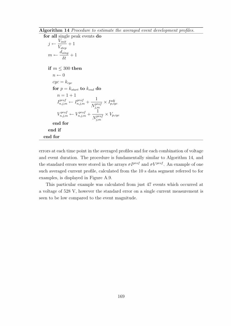
Algorithm 14 Procedure to estimate the averaged event development profiles.
for all single peak events do
j ← VinitVstep
+ 1
m← dsingδt
+ 1
if m ≤ 300 then
n← 0
cyc = kcyc
for p = kstart to kend do
n = 1 + 1
Iprofn,j,m ← Iprofn,j,m +1
Nprofj,m
× Iadjp,cyc
V profn,j,m ← V prof
n,j,m +1
Nprofj,m
× Vp,cyc
end for
end if
end for
errors at each time point in the averaged profiles and for each combination of voltage
and event duration. The procedure is fundamentally similar to Algorithm 14, and
the standard errors were stored in the arrays σIprof and σV prof . An example of one
such averaged current profile, calculated from the 10 s data segment referred to for
examples, is displayed in Figure A.9.
This particular example was calculated from just 47 events which occurred at
a voltage of 528 V, however the standard error on a single current measurement is
seen to be low compared to the event magnitude.
169
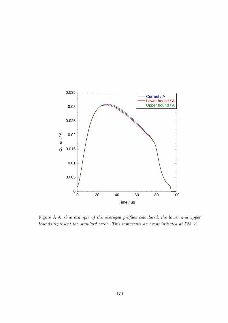
0
0.005
0.01
0.015
0.02
0.025
0.03
0.035
0 20 40 60 80 100
Current / ALower bound / AUpper bound / A
Cu
rre
nt / A
Time / µs
Figure A.9: One example of the averaged profiles calculated, the lower and upper
bounds represent the standard error. This represents an event initiated at 528 V.
170

Appendix B
Data analysis procedures for
in-situ discharge monitoring
experiments.
Whilst similar in many respects to the processing of data from single discharge
experiments, the data from in-situ monitoring required slightly different analysis.
This was in part due to the requirement that the signal from the current probe be
corrected for the distortion resulting from LR droop.
B.1 Correction for current probe frequency ef-
fects.
The current during in-situ discharge monitoring experiments was measured using
a Tektronix P6021 current probe and a Picoscope 5203 digital oscilloscope. The
current probe was non-contact, relying on the electrical induction. As mentioned
in section 3.2, four loops of the signal wire were passed through the current probe,
giving an effective resolution of 2 mV per 1 mA. The probe is designed to be used
with periodic signals, and the lower bandwidth cut off specified by the manufacturer
was 400 Hz.
Even signals at greater then 400 Hz will suffer from distortions, especially if the
signals contain sections where the current signal is not changing in time. For exam-
ple a square wave signal will show exponential LR decay of the current indicated
by the probe during the period of constant current.
The discharge events were detected as short pulses, with a total duration short
enough that detection by the probe was not problematic. However the LR decay
over the peak of the event, when the current gradient was low, led to distortion of the
171
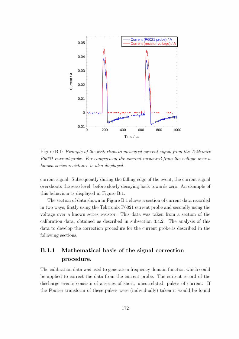
-0.01
0
0.01
0.02
0.03
0.04
0.05
0 200 400 600 800 1000
Current (P6021 probe) / ACurrent (resistor voltage) / A
Cu
rre
nt / A
Time / µs
Figure B.1: Example of the distortion to measured current signal from the Tektronix
P6021 current probe. For comparison the current measured from the voltage over a
known series resistance is also displayed.
current signal. Subsequently during the falling edge of the event, the current signal
overshoots the zero level, before slowly decaying back towards zero. An example of
this behaviour is displayed in Figure B.1.
The section of data shown in Figure B.1 shows a section of current data recorded
in two ways, firstly using the Tektronix P6021 current probe and secondly using the
voltage over a known series resistor. This data was taken from a section of the
calibration data, obtained as described in subsection 3.4.2. The analysis of this
data to develop the correction procedure for the current probe is described in the
following sections.
B.1.1 Mathematical basis of the signal correction
procedure.
The calibration data was used to generate a frequency domain function which could
be applied to correct the data from the current probe. The current record of the
discharge events consists of a series of short, uncorrelated, pulses of current. If
the Fourier transform of these pulses were (individually) taken it would be found
172

to contain components across a range of frequencies. The lower band cut off for
the current probe is 400 Hz, this does not mean that the probe does not detect
frequencies below that (any non-DC components will couple to an extent), but
below the cut off the frequency components of the signal suffer distortions in both
amplitude and phase. It is these distortions in the low frequency components of the
signal which cause the problems visible in Figure B.1, and which must be removed
from the signal to obtain the discharge currents accurately.
The first step is to find sections within the calibration data which can be con-
sidered to be independent. As can be seen in Figure B.1, after each discharge event
the current probe signal overshoots the zero level before it begins to decay upwards
back to zero. Any section of data which begins with the initiation of a discharge
event, and ends with the return of the current probe signal back to the zero level can
be considered independent, as subsequent discharge events are not impacted by the
signal of previous events. By contrast, if a discharge event initiates before the cur-
rent probe signal has returned to zero, then the starting level of the new discharge
is influenced by the previous events and hence cannot be considered independent.
A sample of the current record from the resistor will be referred to as Iresj
and from the current probe as Iprobej . If an independent section of current data
is considered, of total length Nind samples, then the Discrete Fourier Transform
(DFT) can be determined as in Equation B.1.
xk =
Nind∑j=1
xj exp
(−2πi (j − 1) (k − 1)
Nind
)(B.1)
In practical terms if the signal under consideration returns to zero after a finite
duration, then that signal can be padded with zeros (by adding them to the end)
to increase Nind. This padding is required to ensure the DFT represents an approx-
imation to the Fourier transform (which is like a Fourier series of infinite period).
If the signal is not padded with zeros then the DFT is an approximation to the
Fourier series of the signal instead, if it were to be repeated with period equal to
the signal length.
It will be assumed that the period of zero signal after the current pulse is suffi-
cient that calculation of the DFT yields an approximation to the Fourier transform
of the transient signal. If the DFT is calculated for both Iresj and Iprobej , then the
ratio of the components Iresk and Iprobek can be taken according to Equation B.2 to
give an estimation of the amplitude ratio and phase shift between components of
the signal and the current probe response. The vector FR is a complex number, the
components of which then represent an approximation to the frequency response of
173

the current probe and wire coil system.
FRk =Iresk
Iprobek
(B.2)
The calculated frequency response function, FR, can then be used to estimate
the probe response to an applied signal, or in this case to estimate the signal which
gives rise to a certain response from the current probe. This is done by taking
the DFT of the probe signal to yield Iprobek , multiplying each component by the
corresponding value of FR, then taking the inverse DFT to yield an estimate of the
true current signal, with Icorrj representing the corrected current signal, calculated
according to Equation B.3.
Icorrj =1
Nind
Nind∑k=1
(Iprobek × FRk
)exp
((2πi (j − 1) (k − 1))
Nind
)(B.3)
This procedure suffers from many problems when implemented on the in-situ
monitoring data. The correction is sensitive to the quality of the FR function which
can be calculated from the calibration data. The measured signals both have errors
associated with them, low level noise, and the 8-bit digitisation makes the data
seem stepped. The 8-bit and stepped nature of data introduces sometimes severe
fluctuations in the regions of the DFT corresponding to high frequency components.
The extent to which the DFT can be taken as an approximation of the Fourier
transform is to a degree dependent upon the number of zeros with which the sig-
nal is padded. More zeros after the signal itself is generally going to represent a
better approximation to the Fourier transform (effectively extending the periodic-
ity towards infinity). However in practice the extent of such padding is limited by
the requirements of computing time, and in this case a balance had to be struck
between robustness of the correction and the time required.
In the following sections the procedures applied to estimate the probe frequency
response function will be outlined, and the limitations discussed in greater detail.
The quality of the FR function generated will be tested by application back to the
raw calibration data and calculation of the deviation of Icorr from Ires.
B.1.2 Scaling of variables and determination of threshold
values.
In the in-situ logging, data analysis will focus upon the periods of positive sample
polarity. These represent roughly two thirds of each cycle of 20 ms. With sampling
every 2 µs this is 10 000 samples per process cycle, and approximately 6600 samples
during positive polarity. Discharging activity never extended to the end of positive
174
polarity, and generally there was an appreciable period of zero activity between
cessation of discharge activity and the voltage passing through zero.
In light of the requirement that the processing not take an infeasible period of
time, it was decided not to pad the signal data from each positive cycle beyond
that already provided by the natural quenching of discharge activity. It was also
decided that any interpolation of the FR function would be undesirable. The regions
of interest in the calibration data then represented those sections of data with
length 6600 samples and which could be considered to be independent. As discussed
previously, for a section to be independent it is required that both the start and end
of the section have zero value of both the current probe signal and the gradient of the
current probe signal. This allows estimation of a frequency response of the current
probe, FR, which can be applied to the experimental data without interpolation.
The raw data from which the calibration is to be calculated required scaling,
and determination of threshold values prior to indexing of regions of interest. This
was done in a broadly similar fashion to the single discharge case, though sufficient
differences exist between the procedures to be worth repeating some elements. The
vector containing the current probe data was called A in this case, corresponding
to the first channel of the oscilloscope, the vector B was the voltage over the 200 Ω
resistor. The scaling was as detailed in Equation B.4.
Iprobej = Aj × 0.5 ∀ j
Iresj =Bj
200∀ j
(B.4)
The minimum detectable current shifts for each current record were also defined,
according to Equation B.5. A gradient measure was also calculated for the Iresj ,
using the same procedure as detailed in subsection A.1.2. This gradient measure,
dIresj , was again used to compile a list of stationary points, as in subsection A.1.3,
and a histogram of the current values at stationary points calculated. The baseline
level, Ibase, was defined as before, and so were the threshold value, Ithresh and the
minimum shift Ishift. All three refer only to the current data obtained from the
resistor measurement.
Iprobestep =100× 10−3
127
Iresstep =20/200
127
(B.5)
One variable calculated during this stage of the procedure, which has no analogy
for single discharge processing, was a running average of the current probe signal,
175

covering the current sample and 9 previous samples. This was defined according
to Algorithm 15, in which N is again the total record length. This vector will be
later used as part of a condition to determine whether the current probe signal has
returned to zero signal.
Algorithm 15 Calculation of current probe signal running average.
Iavg is a vector of length N , initialised to contain all zeros
for all 10 ≥ j ≤ N do
for m = 0 to 9 do
Iavgj ← Iavgj + 0.1Iprobej−m
end for
end for
B.1.3 Indexing of independent regions.
The indexing of 6600 sample independent regions is required in order that the
frequency response of the current probe can be determined. Many parts of this
procedure are sufficiently similar to many of the elements of the single discharge
event indexing that detailed textual descriptions and illustrative examples will not
be provided in this case. The important difference is that this procedure is trying
to identify regions which begin with initiation of a discharge event at a time when
Iprobej is equal to zero, and terminate when the probe current has again returned
to zero. As is evident from Figure B.1, this often did not occur until some time
after termination of the actual event, and sometimes another event would initiate
before Iprobej was again zero. Two events whose signals in the current probe record
overlapped in this fashion cannot be regarded as independent signals since the first
has influenced the starting signal level of the second. The initial identification of
discharge events was as detailed in Algorithm 16.
Up to this point the indexing procedure is similar to that adopted for single
discharge data. Now the process diverges significantly as the indexing must be
extended from the start of each discharge event up until the point where the subse-
quent recorded data may once again be considered independent of the proceeding
signal. The procedure to extend the tail ends of regions indexed in the G variable
is detailed in Algorithm 17.
One feature of the procedure which requires clarification is why the next 30
samples worth of data were automatically set as true after the start of each discharge
event. This was because the running average, Iavgj , would pass through zero value
around the endpoint of the discharge event, however this happened as the current
176

Algorithm 16 Initial identification of discharge events.
G will again denote a logical indexing vector, initialised to all zeros
for j = 1 to N do
if Iresj > Ibase + Ishift then
Gj ← 1
end if
end for
extension of indexing to cover the rising discharge edge
for j = N to 2 do
if Gj = 1 AND Gj−1 = 0 AND dIresj−1 > 0 then
Gj−1 ← 1
end if
end for
probe signal, Iprobej was overshooting the zero level. Conditions to account for
this which were based around the 4th order finite difference gradient of Iprobej were
found to be inadequate. The addition of the next 30 samples after the currently
indexed termination of regions, which prior to this condition is the point where
Iprobej drops below Ibase + Ishift, enabled this problematic region to be removed
from consideration. From this point onwards the extension of indexing in vector
G to cover up until Iprobej returns to zero can be performed without concern over
mis-identification.
The regions of independent signal held in G can now be listed in variable index
using a listing routine identical to that detailed in subsection A.1.9, with the listing
variable having the same structure as in that subsection. After listing, any identified
regions over which the maximum to minimum variation in Iprobej is less than 5Iprobestep
are removed from the indexing vector G by setting all associated Gj = 0. A short
representative section showing this indexing is displayed in Figure B.2.
B.1.4 Final identification of usable sections and calculation
of frequency response function.
The final task before the estimation of the frequency response of the current probe
is to identify sections of 6600 samples duration which start and end in regions
where Gj = 0, and in which some discharge events were included. This procedure
is outlined in Algorithm 18.
177

Algorithm 17 Extension of the indexing to cover entire independent regions.
need to locate all end-points in the current indexing
let Nevent denote the number of regions indexed in G
list end points in vector list, of length Nevent
m← 0
for j = 2 to N do
if Gj = 0 AND Gj−1 = 1 then
m← m+ 1
listm ← j
end if
end for
extend indexing at all endpoints by 30 samples
for j = 1 to Nevent do
for all listj ≥ m ≤ listj + 30 do
Gm ← 1
end for
end for
extend indexing to point where subsequent data is independent
for j = 2 to N do
if Gj−1 = 1 AND Gj = 0 AND Iavgj ≤ 0− 0.25Iprobestep then
Gi ← 1
end if
end for
178

Algorithm 18 Identification and listing of usable regions.
let Guse denote a second logical index vector, length N
Nscale ← 6600
for j = 2 to N −Nscale do
temp← Gusej−1 +Guse
j +Gusej+1
if temp = 0 AND Gj = 0 AND Gj+Nscale−1 = 0 then
if Gm = 1 at some point between m = j and m = j +Nscale − 1 then
for all j ≥ m ≤ j +Nscale − 1 do
Gusem ← 1
end for
end if
end if
end for
now list start and end coordinates of usable regions
use listing array indexuse for this purpose
m← 0
for j = 2 to N do
if Gusej = 1 AND Guse
j−1 = 0 then
m← m+ 1
indexusem,1 ← j − 1
else if Gusej = 0 AND Guse
j−1 = 1 then
indexusem,2 ← j
end if
end for
179

-0.02
-0.01
0
0.01
0.02
0.03
0.04
0.05
0.06
-0.2
0
0.2
0.4
0.6
0.8
1
1.2
0 2000 4000 6000 8000 10000 12000 14000
Current (P6021 probe) / ACurrent (resistor voltage) / A
Logical index G
Cu
rre
nt / A
Lo
gic
al in
dex G
Time / µs
Figure B.2: Example of the indexing of regions which may be considered related
by the current probe signal, Iprobej . Three separate independent blocks of discharge
activity can be seen.
The procedure finds regions of 6600 samples in length which start and end from
Iprobej = 0, and which contain at least one discharge event. These regions can be
used to estimate the frequency response by calculating the DFT of both Iprobe and
Ires. The DFT was calculated using the fast Fourier transform algorithm supplied
with the Matlab 7 software package. For each usable region identified, the ratio
between Iresk and Iprobek was taken for all k. All such estimated frequency responses
were stored, and then used to calculate an averaged frequency response from all the
usable regions. The procedure for this is outlined in Algorithm 19.
In total there were 2101 usable regions, and an averaged frequency response
function was calculated from these. This was done by calculation of the mean FRk
value for each k. The averaged frequency response function will be termed fr from
now onwards. The frequency response function contains unique information only
up to the Nyquist frequency, 250 kHz in this case. At most frequencies the function
is essentially uninteresting, with amplitude close to 1, and phase shift close to zero.
At lower frequencies the amplitude ratio and phase shifts become large. It is these
lower frequency components of the signal which require correction in the current
probe data. The amplitude and phase angle of the function fr and a function of
frequency are presented in Figure B.3.
180

Algorithm 19 Calculation of the frequency response function.
Nuse is the number of usable regions identified
F [X] will indicate the fast Fourier transform of vector X
IR indicates the current probe response vector in usable region
IS indicates the series resistor current probe in usable region
for j = 1 to Nuse do
p← 0
for m = indexusej,1 to indexusej,2 do
p← p+ 1
IRp ← Iprobem
ISp ← Iresm
end for
IR ← F[IR]
IS ← F[IS]
let FR be the frequency response data array, dimension 6600 rows and Nuse
columns
for m = 1 to Nscale do
FRm,j ←ISmIRm
end for
end for
181

0
1
2
3
4
5
6
0 5000 10000 15000 20000 25000 30000 35000
amplitude ratio
am
plit
ud
e r
atio
Frequency / Hz
-1.5
-1
-0.5
0
0 5000 10000 15000 20000 25000 30000 35000
phase angle / radians
ph
ase a
ngle
/ r
adia
ns
Frequency / Hz
a)
b)
Figure B.3: The low frequency end of the frequency response function, fr, calculated
for the current probe from the calibration data.
182
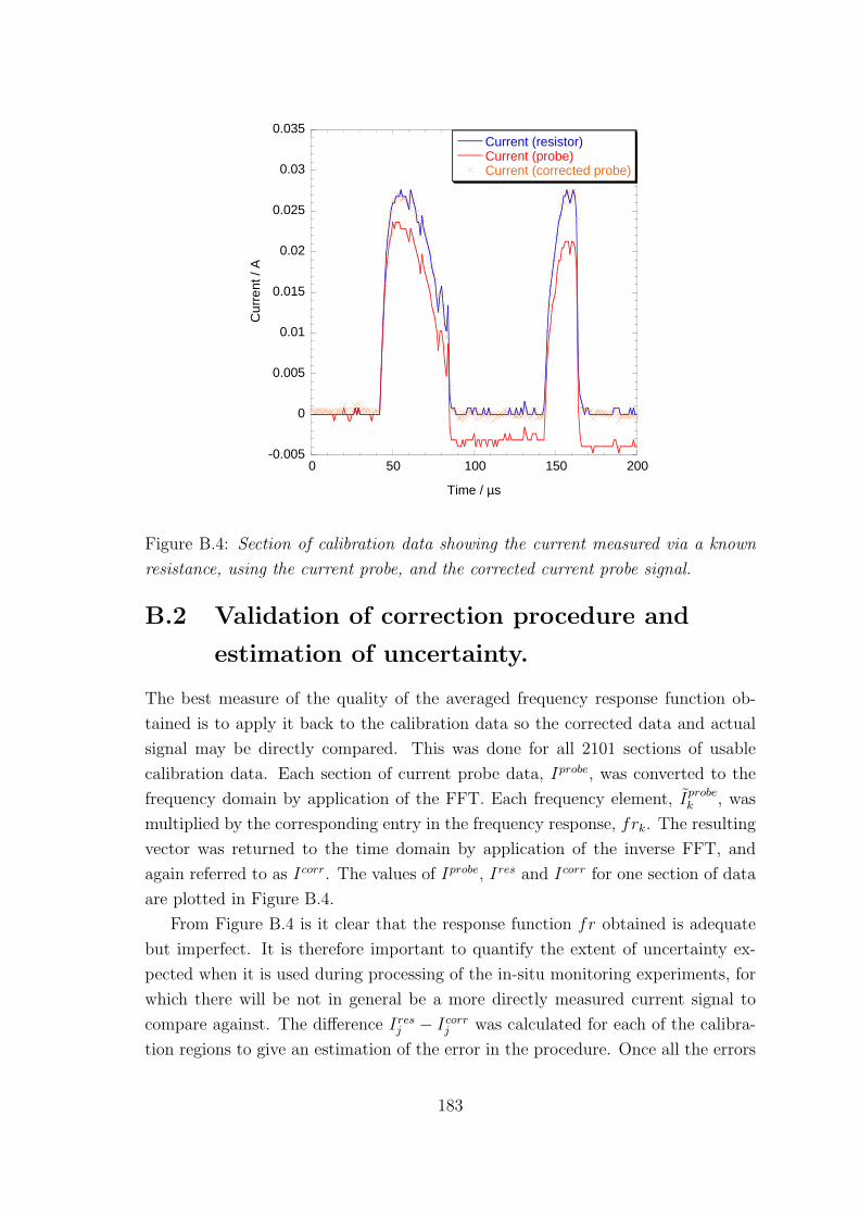
-0.005
0
0.005
0.01
0.015
0.02
0.025
0.03
0.035
0 50 100 150 200
Current (resistor)Current (probe)Current (corrected probe)
Cu
rre
nt / A
Time / µs
Figure B.4: Section of calibration data showing the current measured via a known
resistance, using the current probe, and the corrected current probe signal.
B.2 Validation of correction procedure and
estimation of uncertainty.
The best measure of the quality of the averaged frequency response function ob-
tained is to apply it back to the calibration data so the corrected data and actual
signal may be directly compared. This was done for all 2101 sections of usable
calibration data. Each section of current probe data, Iprobe, was converted to the
frequency domain by application of the FFT. Each frequency element, Iprobek , was
multiplied by the corresponding entry in the frequency response, frk. The resulting
vector was returned to the time domain by application of the inverse FFT, and
again referred to as Icorr. The values of Iprobe, Ires and Icorr for one section of data
are plotted in Figure B.4.
From Figure B.4 is it clear that the response function fr obtained is adequate
but imperfect. It is therefore important to quantify the extent of uncertainty ex-
pected when it is used during processing of the in-situ monitoring experiments, for
which there will be not in general be a more directly measured current signal to
compare against. The difference Iresj − Icorrj was calculated for each of the calibra-
tion regions to give an estimation of the error in the procedure. Once all the errors
183
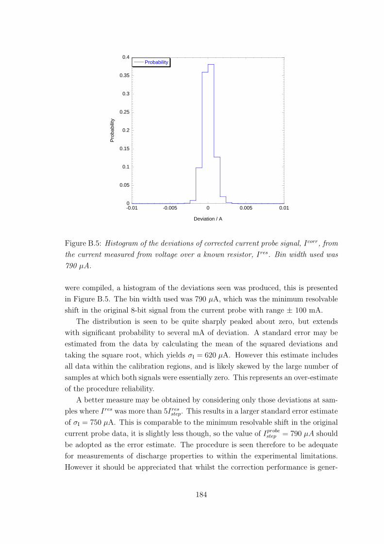
0
0.05
0.1
0.15
0.2
0.25
0.3
0.35
0.4
-0.01 -0.005 0 0.005 0.01
Probability
Pro
ba
bili
ty
Deviation / A
Figure B.5: Histogram of the deviations of corrected current probe signal, Icorr, from
the current measured from voltage over a known resistor, Ires. Bin width used was
790 µA.
were compiled, a histogram of the deviations seen was produced, this is presented
in Figure B.5. The bin width used was 790 µA, which was the minimum resolvable
shift in the original 8-bit signal from the current probe with range ± 100 mA.
The distribution is seen to be quite sharply peaked about zero, but extends
with significant probability to several mA of deviation. A standard error may be
estimated from the data by calculating the mean of the squared deviations and
taking the square root, which yields σI = 620 µA. However this estimate includes
all data within the calibration regions, and is likely skewed by the large number of
samples at which both signals were essentially zero. This represents an over-estimate
of the procedure reliability.
A better measure may be obtained by considering only those deviations at sam-
ples where Ires was more than 5Iresstep. This results in a larger standard error estimate
of σI = 750 µA. This is comparable to the minimum resolvable shift in the original
current probe data, it is slightly less though, so the value of Iprobestep = 790 µA should
be adopted as the error estimate. The procedure is seen therefore to be adequate
for measurements of discharge properties to within the experimental limitations.
However it should be appreciated that whilst the correction performance is gener-
184
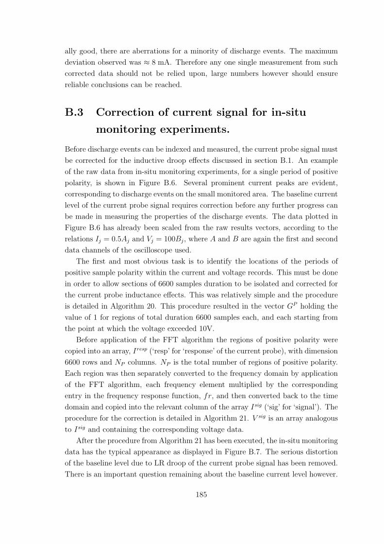
ally good, there are aberrations for a minority of discharge events. The maximum
deviation observed was ≈ 8 mA. Therefore any one single measurement from such
corrected data should not be relied upon, large numbers however should ensure
reliable conclusions can be reached.
B.3 Correction of current signal for in-situ
monitoring experiments.
Before discharge events can be indexed and measured, the current probe signal must
be corrected for the inductive droop effects discussed in section B.1. An example
of the raw data from in-situ monitoring experiments, for a single period of positive
polarity, is shown in Figure B.6. Several prominent current peaks are evident,
corresponding to discharge events on the small monitored area. The baseline current
level of the current probe signal requires correction before any further progress can
be made in measuring the properties of the discharge events. The data plotted in
Figure B.6 has already been scaled from the raw results vectors, according to the
relations Ij = 0.5Aj and Vj = 100Bj, where A and B are again the first and second
data channels of the oscilloscope used.
The first and most obvious task is to identify the locations of the periods of
positive sample polarity within the current and voltage records. This must be done
in order to allow sections of 6600 samples duration to be isolated and corrected for
the current probe inductance effects. This was relatively simple and the procedure
is detailed in Algorithm 20. This procedure resulted in the vector GP holding the
value of 1 for regions of total duration 6600 samples each, and each starting from
the point at which the voltage exceeded 10V.
Before application of the FFT algorithm the regions of positive polarity were
copied into an array, Iresp (‘resp’ for ‘response’ of the current probe), with dimension
6600 rows and NP columns. NP is the total number of regions of positive polarity.
Each region was then separately converted to the frequency domain by application
of the FFT algorithm, each frequency element multiplied by the corresponding
entry in the frequency response function, fr, and then converted back to the time
domain and copied into the relevant column of the array Isig (‘sig’ for ‘signal’). The
procedure for the correction is detailed in Algorithm 21. V sig is an array analogous
to Isig and containing the corresponding voltage data.
After the procedure from Algorithm 21 has been executed, the in-situ monitoring
data has the typical appearance as displayed in Figure B.7. The serious distortion
of the baseline level due to LR droop of the current probe signal has been removed.
There is an important question remaining about the baseline current level however.
185
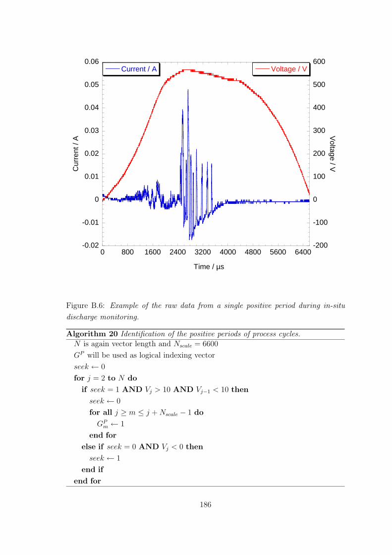
-0.02
-0.01
0
0.01
0.02
0.03
0.04
0.05
0.06
-200
-100
0
100
200
300
400
500
600
0 800 1600 2400 3200 4000 4800 5600 6400
Current / A Voltage / VC
urr
ent / A
Volta
ge / V
Time / µs
Figure B.6: Example of the raw data from a single positive period during in-situ
discharge monitoring.
Algorithm 20 Identification of the positive periods of process cycles.
N is again vector length and Nscale = 6600
GP will be used as logical indexing vector
seek ← 0
for j = 2 to N do
if seek = 1 AND Vj > 10 AND Vj−1 < 10 then
seek ← 0
for all j ≥ m ≤ j +Nscale − 1 do
GPm ← 1
end for
else if seek = 0 AND Vj < 0 then
seek ← 1
end if
end for
186

Algorithm 21 Correction of the current signal.m← 0
for j = 2 to N do
if GPj = 1 AND GP
j−1 = 0 then
m← m+ 1
p← 0
for all j ≥ n ≤ j +Nscale − 1 do
p← p+ 1
Irespp ← In
V sigp ← Vn
end for
end if
end for
apply signal correction procedure
for j = 1 to NP do
for all 1 ≥ m ≤ Nscale do
I tempm ← Irespm,j
end for
I temp ← F [I temp]
for all 1 ≥ k ≤ Nscale do
I tempk ← I tempk × frkend for
I temp ← F−1[I temp
]for all 1 ≥ m ≤ Nscale do
Isigm,j ← I tempm
end for
end for
187
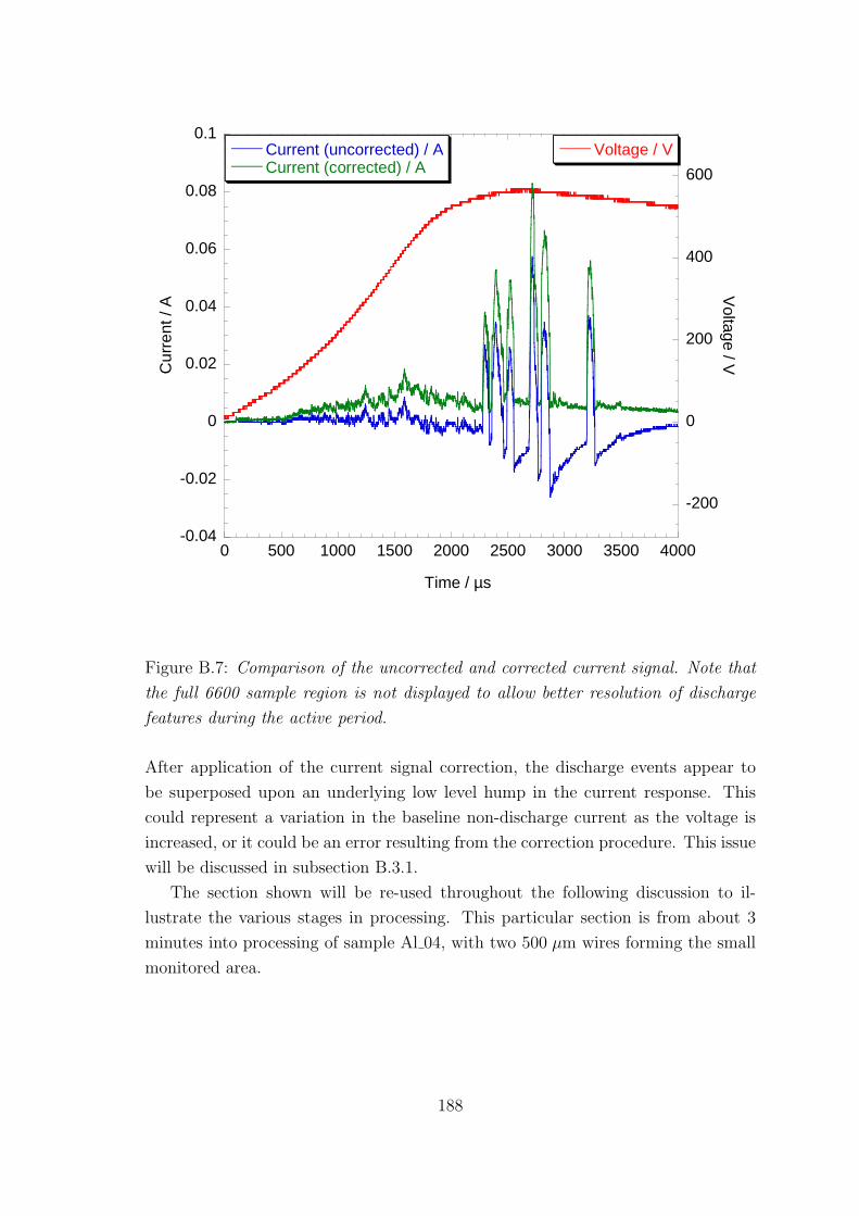
-0.04
-0.02
0
0.02
0.04
0.06
0.08
0.1
-200
0
200
400
600
0 500 1000 1500 2000 2500 3000 3500 4000
Current (uncorrected) / ACurrent (corrected) / A
Voltage / VC
urr
ent / A
Volta
ge / V
Time / µs
Figure B.7: Comparison of the uncorrected and corrected current signal. Note that
the full 6600 sample region is not displayed to allow better resolution of discharge
features during the active period.
After application of the current signal correction, the discharge events appear to
be superposed upon an underlying low level hump in the current response. This
could represent a variation in the baseline non-discharge current as the voltage is
increased, or it could be an error resulting from the correction procedure. This issue
will be discussed in subsection B.3.1.
The section shown will be re-used throughout the following discussion to il-
lustrate the various stages in processing. This particular section is from about 3
minutes into processing of sample Al 04, with two 500 µm wires forming the small
monitored area.
188

B.3.1 Variation of the baseline current during each cycle.
The issue of the baseline level is interesting, however it is unlikely to influence the
eventually measured discharge event properties for two reasons. Firstly if it is an
error then it is on a much longer timescale then any discharge event, and secondly
because the current level at the start of the discharge event must be subtracted from
current during the event in order to measure the event properties accurately. Even
so, it was possible to resolve the issue of whether the current hump represented
a genuine signal or not using a modification of the standard in-situ monitoring
experiment.
As was mentioned in section 3.1, the power unit does not generate the voltage
bias seen during processing. The positive bias is the result of interaction between
power supply and the sample-electrolyte system. This fact can be exploited to allow
limited operation of the in-situ monitoring experiments using a known resistance
in place of the current probe, to obtain more reliable information about the small
area current. This is accomplished by connecting the output bar to ground and
the counter-electrode to the supply output. The output bar now being grounded
allows resistor based current measurement without having to float the oscilloscope
to 600 V. Incidentally this is the reason why a non-contact current probe was used
for the in-situ monitoring generally.
This geometry has a major flaw which means it cannot be used for long periods,
which is that with the counter-electrode connected to the output, the bulk of the
electrolyte is raised to high voltages, meaning that such experiments cannot be run
with the normal processing tank, and the electrolyte cannot be passed through the
heat exchanger without developing a short circuit to ground through the chilled
water system. As a result, long processing periods would overheat. Nonetheless,
by reversing the output and running a short period of processing in an electrically
isolated insert tank, it was possible to obtain data about the current through the
small monitored area which required no correction.
Examination of this data revealed that an increase in the baseline current with
applied voltage is a real feature of the processing. This can be seen in Figure B.8
and Figure B.9. One figure shows a cycle displaying large events, the other only
small discharge events of a few mA at peak. Compared to the current data in
Figure B.7, the hump is of lower magnitude, however this is probably because the
data in Figure B.8 and Figure B.9 are from a sample with only a single 500 µm wire
as small area.
The underlying hump shape visible Figure B.7 is obscured by roughness of the
current signal. This does not represent noise however, as the signal is cleaner when
the voltage is lower. The roughness possibly arises from a number of overlapping
189

0
0.005
0.01
0.015
0.02
0.025
0.03
0.035
0.04
0
100
200
300
400
500
600
0 2000 4000 6000 8000 10000 12000
Current / A Voltage / V
Cu
rre
nt / A
Volta
ge / V
Time / µs
Figure B.8: Example of data from a more reliable current measurement during in-
situ monitoring, showing a cycle containing large discharge events.
190
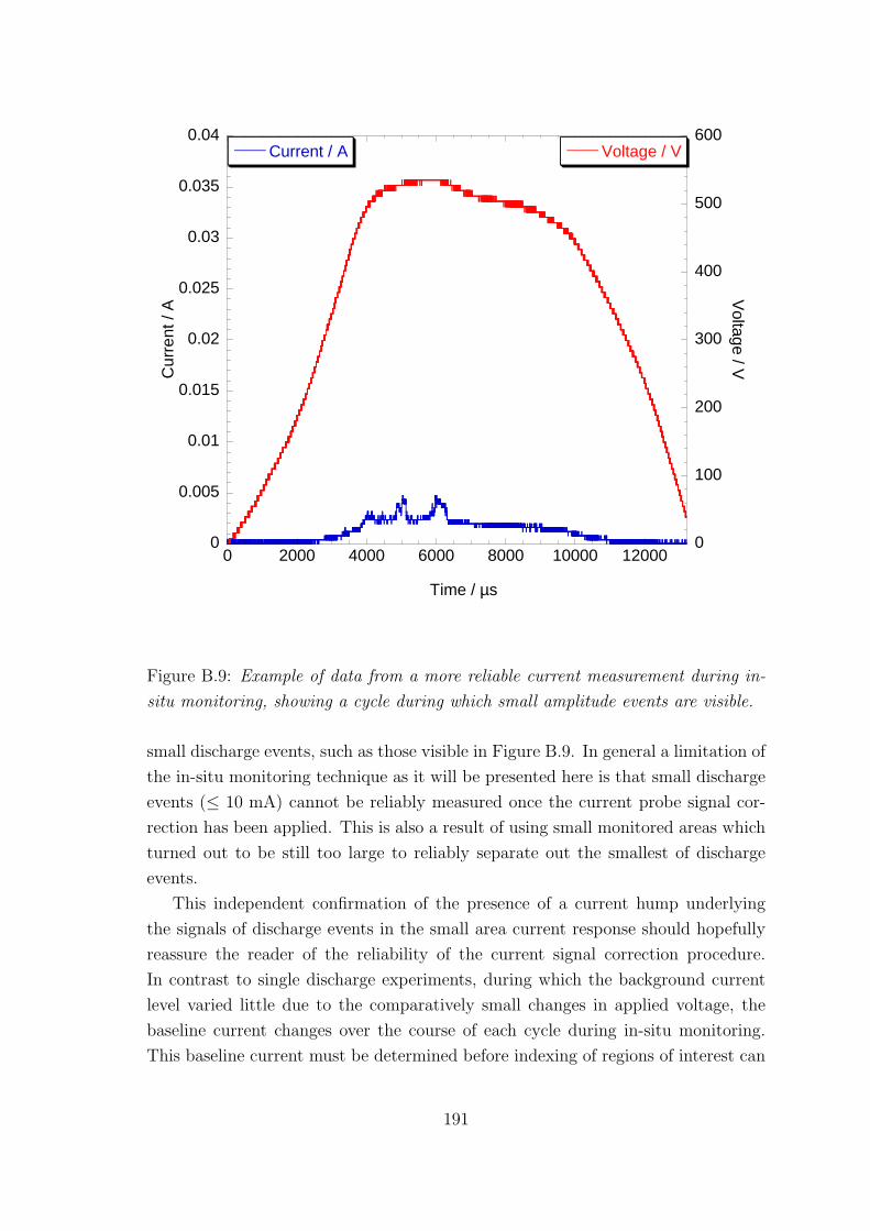
0
0.005
0.01
0.015
0.02
0.025
0.03
0.035
0.04
0
100
200
300
400
500
600
0 2000 4000 6000 8000 10000 12000
Current / A Voltage / VC
urr
ent / A
Volta
ge / V
Time / µs
Figure B.9: Example of data from a more reliable current measurement during in-
situ monitoring, showing a cycle during which small amplitude events are visible.
small discharge events, such as those visible in Figure B.9. In general a limitation of
the in-situ monitoring technique as it will be presented here is that small discharge
events (≤ 10 mA) cannot be reliably measured once the current probe signal cor-
rection has been applied. This is also a result of using small monitored areas which
turned out to be still too large to reliably separate out the smallest of discharge
events.
This independent confirmation of the presence of a current hump underlying
the signals of discharge events in the small area current response should hopefully
reassure the reader of the reliability of the current signal correction procedure.
In contrast to single discharge experiments, during which the background current
level varied little due to the comparatively small changes in applied voltage, the
baseline current changes over the course of each cycle during in-situ monitoring.
This baseline current must be determined before indexing of regions of interest can
191

proceed.
B.4 Adjustment for the baseline current level.
Determination of the baseline current level at each point during a process cycle is
not easy. Such a background can only really be obtained from cycles in which no
discharge events are observed. Determining which cycles contain discharge events
before being in a position to even index discharge event signals leads into a circular
argument. As such the determination of the baseline current waveform is inexact,
and involves several assumptions. The first part of the procedure determines which
process cycles (columns of Isig) are likely to be suitable for estimation of the baseline.
The first stage is to compile a list of the maximum current values during each
cycle, a subsidiary list is then compiled of all the maximum current values which
are below 40 mA. This list is stored as a vector, Imax. The selection of 40 mA as a
cut off for this stage was arbitrary, and made by the author as it worked reasonably
well in testing. In the 20 s segment from which the example plotted in Figure B.7
was taken, the vector Imax had 369 entries, out of 998 process cycles in the entire
segment.
The vector Imax is then used to generate a histogram of the maximum current
during each cycle, using binning of 1 mA. The histogram was then used to deter-
mine the mode value of the maximum current for those cycles without large scale
discharging activity. The mode value plus 2 mA was termed Icyc, and was used in
determination of the baseline current. In the example 20 s segment the value of
the threshold Icyc was 16 mA. The baseline current variation was then estimated
according to Algorithm 22, in which the background current level is stored in the
vector Iback, and Ncyc is the total number of process cycles in the segment, which
was 998 for the example considered.
Vector Iback now contains an estimate of the baseline current variation during
each process cycle (of positive polarity and starting from when the voltage exceeded
10 V). This is assuming that the baseline current level varies only slowly over each
20 s data segment. The baseline current variation determined for the example
segment was calculated from 161 cycles out of 998 overall, and can be seen in
Figure B.10. This background variation was then subtracted from each column of
the array Isig to yield another array, Iadj (in which adj stand for adjusted), and
therefore from each process cycle in the data segment. The appearance of the
example section after this adjustment is presented in Figure B.11.
It can be seen in Figure B.11 that the adjustment is far from perfect. It does
however remove most of the effect of the current hump upon which the signals of
192

Algorithm 22 Estimation of the cycle baseline current variation.
the number of cycles which meet condition to be included is pre-determined and
stored as the variable Ncount
for j = 1 to Ncyc do
Ipeak ← maximum current value in column j of array Isig
if Ipeak ≤ Icyc then
for all 1 ≥ m ≤ Nscale do
Ibackm ← Ibackm +1
Ncount
× Isigm,jend for
end if
end for
0
0.005
0.01
0.015
0.02
0 2000 4000 6000 8000 10000 12000
Current / A
Cu
rre
nt / A
Time / µs
Figure B.10: The estimated current background variation, Iback, calculated from all
the cycles in the 20 s example segment.
193

0
0.01
0.02
0.03
0.04
0.05
0.06
0.07
0.08
0
100
200
300
400
500
600
700
0 1000 2000 3000 4000 5000 6000 7000 8000
Current / A Voltage / V
Cu
rre
nt / A
Volta
ge / V
Time / µs
Figure B.11: The current and voltage signals after adjustment to remove the esti-
mated background current variation.
194
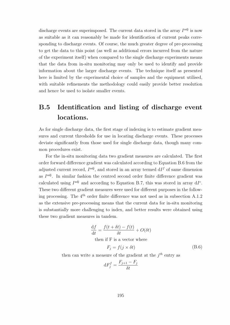
discharge events are superimposed. The current data stored in the array Iadj is now
as suitable as it can reasonably be made for identification of current peaks corre-
sponding to discharge events. Of course, the much greater degree of pre-processing
to get the data to this point (as well as additional errors incurred from the nature
of the experiment itself) when compared to the single discharge experiments means
that the data from in-situ monitoring may only be used to identify and provide
information about the larger discharge events. The technique itself as presented
here is limited by the experimental choice of samples and the equipment utilised,
with suitable refinements the methodology could easily provide better resolution
and hence be used to isolate smaller events.
B.5 Identification and listing of discharge event
locations.
As for single discharge data, the first stage of indexing is to estimate gradient mea-
sures and current thresholds for use in locating discharge events. These processes
deviate significantly from those used for single discharge data, though many com-
mon procedures exist.
For the in-situ monitoring data two gradient measures are calculated. The first
order forward difference gradient was calculated according to Equation B.6 from the
adjusted current record, Iadj, and stored in an array termed dIf of same dimension
as Iadj. In similar fashion the centred second order finite difference gradient was
calculated using Iadj and according to Equation B.7, this was stored in array dIc.
These two different gradient measures were used for different purposes in the follow-
ing processing. The 4th order finite difference was not used as in subsection A.1.2
as the extensive pre-processing means that the current data for in-situ monitoring
is substantially more challenging to index, and better results were obtained using
these two gradient measures in tandem.
df
dt=f(t+ δt)− f(t)
δt+O(δt)
then if F is a vector where
Fj = f(j × δt)then can write a measure of the gradient at the jth entry as
dF fj =
Fj+1 − Fjδt
(B.6)
195

df
dt=f(t+ δt)− f(t− δt)
2δt+O
(δt2)
then if F is a vector where
Fj = f(j × δt)then can write a measure of the gradient at the jth entry as
dF cj =
Fj+1 − Fj−1
2δt
(B.7)
B.5.1 Determination of the current threshold.
As was the case for single discharge data, a threshold value for regions of elevated
current to be indexed as part of a discharge event must be estimated. However,
as has been often mentioned, the more variable nature of the data during each
processing cycle, means that in this case the current threshold is a vector of length
Nscale, allowing different levels of current shift to be indexed as a discharge event in
different regions of each process cycle. This is of course sensitive to the more global
behaviour in the 20 s recorded segment in which a cycle occurred.
The stationary points of the current, as estimated from the gradient measure dIc,
were calculated according to Algorithm 23, in which list is an array of 2 columns
and Nstat rows. Nstat again refers to the total number of stationary points identified
in the current record Iadj. One important difference from the single discharge case
is that the coordinate assigned to each stationary point is a local coordinate to the
previously identified 6600 sample region in which the stationary point lies. The
local nature of the stationary point coordinates will be utilised later.
Once the listing of stationary points is completed, the determination of the
current threshold may proceed. Threshold current values are calculated for different
parts of each process cycle, and the cycle is broken down into 66 evenly spaced sub-
regions of 100 samples for this purpose. In this context I thresh will represent a vector
of 66 entries, one entry to hold the threshold value for each part of the processing
cycle. The vector Ibins is a list of bin midpoints for calculating histograms, running
from -20 mA to +150 mA with spacing Istep = 0.79 mA. The total number of bins
is termed Nbins. The procedure for calculating I thresh is detailed in Algorithm 24.
The procedure of Algorithm 24 is similar to the threshold determination of single
discharge events detailed in subsection A.1.4. However it is separately carried out for
each small section of the process cycle. In each 100 sample subregion the threshold
is defined as either the minimum between the fluctuation about the baseline at that
point and a second peak, or if that does not exist the maximum value at which a
stationary point in dIc was observed. A minimum value of 5 mA is accepted for
the local value of I thresh. The I thresh vector is then smoothed over a period of 3
196

Algorithm 23 Generation of list of stationary current values.p← 0
for j = 1 to Ncyc do
for m = 2 t Nscale do
if (dIcm,j < 0 AND dIcm−1,j > 0) OR (dIcm,j > 0 AND dIcm−1,j < 0) then
p← p+ 1
if | dIcm,j |<| dIcm−1,j | then
listp,1 ← Isigm,jlistp,2 ← m
else
listp,1 ← Isigm−1,j
listp,2 ← m− 1
end if
end if
end for
end for
samples, and a condition applied that at no point can the local value be less than
two thirds of the maximum I thresh value.
After that, the vector I thresh is padded to make it Nscale values in total length.
The threshold vector is calculated with respect to the entire 20 s data segment, and
then applied to each cycle individually. An example of the threshold level vector,
plotted with the example cycle for comparison, is found in Figure B.12. The current
threshold is seen to show slight increases in value during parts of the cycle which
had a tendency to be noisier, within the approximately 1000 cycles in the respective
20 s segment of the recording. These are only small increases, however it was found
in practice to dramatically reduce the number of artefacts in the discharge indexing.
As was discussed before, the ‘noisy’ period towards the start of each cycle is
probably not noise, but rather many very small discharge events which overlap.
Nonetheless, the experimental set-up used could not resolve these events properly,
and so the indexing algorithms should not be identifying such small fluctuations as
discharge events, as the data obtained would contain no sensible information.
B.5.2 Initial indexing and listing of discharge events.
The initial indexing was simple, with a sample being assigned as part of a discharge
event if the current was in excess of, or equal to, the local current threshold. This
was done for each column of the current array Iadj. The indexing was stored in a
logical array, termed G, of equivalent dimensions to Iadj, with a value of 1 indicating
197

Algorithm 24 Estimation of current threshold values for each point in the process
cycle.
for j = 1 toNscale
100do
let temp be a temporary listing vector used in computation
p← 0
kstart ← (j − 1)× 100 + 1
kend ← j × 100
for m = 1 to Nstat do
if listm,2 > kstart AND listm,2 ≤ kend then
p← p+ 1
tempp ← listm,1
end if
end for
hist← calculated histogram of values stored in temp with bins centred around
Ibins values
kmax ← coordinate of maximum value of histp for 1 ≥ p ≤ Nbins
seek ← 1
for m = kmax to Nbins − 1 do
if seek = 1 then
if histm = 0 OR histm < histm+1 then
I threshj ← Ibinsm
end if
end if
end for
if I threshj < 5× 10⁻³ then
I threshj ← 5× 10⁻³
end if
end for
temp = I thresh
for all 2 ≥ j ≤ Nscale
100− 1 do
I threshj ← 13
(tempj−1 + tempj + tempj+1)
end for
I threshmax ← maximum value stored in I thresh
for all 1 ≥ j ≤ Nscale
100do
if I threshj < 23I threshmax then
I threshj ← 23I threshmax
end if
end for
198

0
0.01
0.02
0.03
0.04
0.05
0.06
0.07
0.08
0 1000 2000 3000 4000 5000 6000 7000 8000
Current / ACurrent threshold / A
Cu
rre
nt / A
Time / µs
Figure B.12: The current threshold for the 20 s data segment from which our example
cycle is drawn, plotted for comparison with the example cycle current signal.
199

Column Measurement Symbol Unit
1 Cycle number kcyc integer
2 Initiation coordinate within cycle kstart integer
3 Termination coordinate within cycle kend integer
4 Initiation current level Istart A
5 Termination current level Iend A
6 Average baseline current Ibase A
7 Peak current minus averaged baseline Ipeak A
Table B.1: Properties stored in the columns of the listing array index.
inside an event and the value 0 outside. A figure representing the output of this pro-
cedure will not be produced, as it should be evident from inspection of Figure B.12
which parts of the example cycle will be indexed as above the threshold, I thresh.
In the section which will follow, a process which will be repeated often is the
listing of discharge event locations, as indexed in array G, and the measurement
of some selected properties of the events as currently indexed. The list will be in
the form of an array termed index, of dimension 7 columns and Nevent rows. The
details of which measures will be stored in which column of the listing variable
are shown in Table B.1. These measurements were used primarily to allow for
screening conditions to be applied to the listed discharge events at various points
during indexing.
The procedure for generating the index array is outlined in Algorithm 25. This
procedure will be referred to many times later on in the indexing process. The first
three columns allow the event to be located by listing first the cycle within the wider
20 s segment in which the event occurs, then the local coordinates of initiation and
termination of the event within the specified process cycle.
Knowledge of the initiation and termination currents is an important quality
control measure. Whilst the baseline level is varying all the time slightly, if the in-
dexed start and end currents differ by much more than a few times Istep = 0.79 mA,
it likely indicates a problem with the indexing of that event. The average of the
start and end currents defines a local baseline level for current, which can be used to
estimate the current level due to the discharge alone. The maximum current shift
due to the discharge event is important, as events which demonstrate too low a
level of current variation are unlikely to be reliably indexed discharge events. After
application of the initial indexing and listing, in the 20 s segment from which the
example section is drawn there were 6766 discharge events indexed.
200

Algorithm 25 Generation of listing array of indexed discharge events.p← 0
seek ← 0
for j = 1 to Ncyc do
for m = 2 to Nscale do
if seek = false then
if Gm,j = 1 AND Gm−1,j = 0 then
p← p+ 1
seek ← 1
indexp,1 ← j
indexp,2 ← m
indexp,4 ← Iadjm,j
end if
else
if Gm,j = 0 AND Gm−1,j = 1 then
seek ← 1
indexp,3 ← j − 1
indexp,5 ← Iadjm−1,j
end if
end if
end for
end for
for j = 1 to Nevent do
indexj,6 ←indexj,4 + indexj,5
2Imax ← maximum value of Iadjm,j over range indexj,2 ≥ m ≤ indexj,3
indexj,7 ← Imax − indexj,6end for
201

B.5.3 Common procedures for finalisation of indexing.
The listing procedure detailed in Algorithm 25 is one example of a repeated proce-
dure during indexing of discharge event current signatures. There were three other
commonly repeated procedures, and these will detailed and explained before their
usage in finalising the indexing of discharge events is outlined in subsection B.5.4.
B.5.3.1 Splitting of independent peaks.
As was discussed in subsection B.5.1, the estimation of a baseline current variation
was vital, but far from perfect. One way in which it was often found to fail was the
case of two large and clearly distinct current peaks, separated by a period of a few
tens of µs of baseline current which was locally in excess of the previously estimated
baseline level. This can occur in a number of ways. Firstly every cycle was different
and the baseline level did vary. Secondly the procedure used to correct the current
probe signal for inductance effects was also not perfect.
Algorithm 26 Splitting of independent peaks separated by higher than usual baseline
current.for j = 1 to Nevent do
Imax ← maximum value of Iadjm,p for p = indexj,1 and indexj,2 ≤ m ≤ indexj,3
Itemp ← I threshindexj,2
if 0.1× Imax > Itemp then
cycle← indexj,1
for m = indexj,2 to indexj,3 do
if Iadjm,cycle < 0.1× Imax then
Gm,cycle←0
end if
end for
end if
end for
In these situations the large peaks separated by baseline current slightly above
the initial threshold level will all be indexed as a single event. To eliminate such
artefacts a procedure and set of conditions were developed which allow the current
peaks to be separated. This procedure is detailed in Algorithm 26, and was executed
at several stages during processing of the data.
The splitting procedure takes 10% of the maximum current shift, from the ini-
tiating current to the peak current, as an alternative threshold value, if that 10%
value is greater than the local current threshold stored in the vector I thresh. This
will allow plateau regions between independent current peaks, where the plateau
202

region of baseline current is unusually high and not identified correctly. The initial
threshold value was no more than a guess to begin with, and cannot be guaranteed
to be accurate during every process cycle.
The application of the splitting procedure will of course affect indexing of many
events (by reducing the extent of indexing of rising and falling edges in many cases).
However in practice its use is always coupled to other routines designed to extend
discharge event indexing of the rising and falling edges, so such problems are com-
pensated for. That said, all elements of the data processing are imperfect, and small
numbers of artefacts are unavoidable in a dataset of many hundreds of thousands
of discharge events.
B.5.3.2 Extension of rising / falling discharge edge.
The rising and falling edges of indexing of discharge events were extended according
to conditions applied to the gradient measures dIf and dIc calculated before. The
procedure was applied several times to both rising and falling discharge edges, and
is detailed in Algorithm 27.
The variable sense takes the value either 1 or −1 depending on whether the
falling or rising edge respectively is being extended. The gradient threshold dIthresh =
(0.5×10⁻³)/δt, with δt = 2 µs, is used during the procedure as a threshold value. If
the magnitude of the gradient falls below this value then the initiation / termination
point of the discharge event is deemed to have been reached.
B.5.3.3 Extension of rising / falling edge until close to ending / starting
current level.
Another procedure carried over from the single discharge case, with suitable mod-
ifications, was the extension of the falling edge to within a certain current of the
initiation level. For the in-situ monitoring data it was also required to extend the
rising edge to within a certain current of the termination current. This procedure
was required as fluctuations and plateaus in discharge event signals meant it was
reasonably common for only one out of the initiation or termination points to be
readily located.
In such cases application of the procedure detailed in Algorithm 28 for sense = 1
and Algorithm 29 for sense = −1, usually allowed the indexing to be extended
such that subsequent application of the gradient measure based procedure of sub-
subsection B.5.3.2 allowed correct determination of start and end locations. This
procedure again can be conducted in either sense depending on whether it is desired
to extend the indexing of rising or falling discharge edges.
The procedure in Algorithm 28, for the positive sense, starts from just before
203

Algorithm 27 Extension of rising/falling discharge edge according to current gra-
dient measures.sense← 1 for falling edge OR −1 for rising edge
if sense = 1 then
for j = 1 to Ncyc do
for m = 1 to Nscale − 1 do
if Gm,j = 1 AND Gm+1,j = 0 then
if dIfm+1,j < −dIthresh OR dIcm+1,j < −dIthresh then
Gm+1,j ← 1
end if
end if
end for
end for
else
for j = 1 to Ncyc do
for m = Nscale to 2 do
if Gm,j = 1 AND Gm−1,j = 0 then
if dIfm−1,j > dIthresh OR dIcm−1,j > dIthresh then
Gm−1,j ← 1
end if
end if
end for
end for
end if
204

Algorithm 28 Extension of rising/falling discharge edge according to termina-
tion/initiation current level.
let sense← 1 for falling edge extension
for j = 1 to Nevent do
Itemp ← indexj,4
if Itemp < 0 then
Itemp ← 0
end if
Imax ← maximum value of Iadjm,p for p = indexj,1 and indexj,2 ≤ m ≤ indexj,3
Ireturn ← 0.1× larger of Imax − indexj,4 OR Imax − indexj,5if Ireturn < 3× 10⁻³ then
Ireturn ← 3× 10⁻³
end if
seek ← 1
m← indexj,3 − 2
cyc← indexj,1
while m ≤ Nscale AND seek = 1 do
if Gm,cyc = 0 then
if Iadjj,cyc − Itemp ≥ Ireturn then
Gm,cyc ← 1
else
seek ← 0
end if
end if
end while
end for
205

Algorithm 29 Extension of rising/falling discharge edge according to termina-
tion/initiation current level.
let sense← −1 for rising edge extension
for j = 1 to Nevent do
Itemp ← indexj,5
if Itemp < 0 then
Itemp ← 0
end if
Imax ← maximum value of Iadjm,p for p = indexj,1 and indexj,2 ≤ m ≤ indexj,3
Ireturn ← 0.1× larger of Imax − indexj,4 OR Imax − indexj,5if Ireturn < 3× 10⁻³ then
Ireturn ← 3× 10⁻³
end if
seek ← 1
m← indexj,2 + 2
cyc← indexj,1
while m > 0 AND seek = 1 do
if Gm,cyc = 0 then
if Iadjj,cyc − Itemp ≥ Ireturn then
Gm,cyc ← 1
else
seek ← 0
end if
end if
end while
end for
206

the presently indexed termination point. When a point not indexed as within the
discharge is encountered it is tested to see whether the current is within Ireturn of
the initiating current value. Ireturn is set for each discharge event as either 10% of
the base to peak current difference or 3 mA, whichever is greater. The net result is
that samples neighbouring the previously indexed discharge falling edge are added
to the event until the current level condition is met. The function is similar in the
negative sense for extension of the discharge rising edge 29.
B.5.4 Finalisation of discharge event indexing.
Now that the repeated procedures have been detailed, discussion may return to the
processing of the in-situ monitoring data. At the end of subsection B.5.2 the initial
indexing had been performed, and the listing procedure of Algorithm 25 executed
once. At this stage there were 6766 regions identified in the 20 s segment from
which our example data is taken.
The next stage is to execute Algorithm 26 to split up any peaks separated by
baseline current plateaus which locally exceed I thresh. This increases the number of
indexed regions to 6770 as some regions are split into two or more separate regions.
This is followed by application of the gradient measure based extension of discharge
falling edge by application of Algorithm 27 with sense = 1.
After extension of the discharge falling edges the number of regions indexed has
fallen to 6676, this is due to events which dip just below the local current threshold
being merged once the falling edges are extended. This is followed by the gradient
procedure with sense = −1 to extend the rising edges according to the gradient
measures.
The application of the gradient based extension, after the splitting procedure,
should allow the current initiation and termination points to be located. After this
portion of the processing, the listing procedure of Algorithm 25 must be executed to
update the discharge listing variable index. After the listing has been refreshed the
number of indexed regions has fallen to 5747 for the example segment, the result
of extending the rising edges backwards has been the merging of regions initially
mis-identified as separate regions.
Having executed the gradient based edge extension procedures at least once,
it is likely that most events presently indexed will have either the initiation or
termination point identified correctly. Many events will now already be perfectly
well indexed. The indexing for events not correctly identified yet can be improved
by application of Algorithm 28 with sense = 1 to extend the discharge falling edges.
This merges more regions, resulting in 5536 regions indexed after the procedure.
After extending the falling edges, the indexed rising edges must also be forced
207

to be consistent with the falling edges, and so Algorithm 29 is executed again
with sense = −1. This must be followed by application of the listing procedure,
Algorithm 25, and it is found for our example 20 s segment that the number of
indexed regions has been reduced to 5484 by merging of some regions.
This is followed by a repeat application of Algorithm 27 with sense = 1 and then
again with sense = −1. After this procedure the reduction of regions by mergers is
much smaller, falling slightly to 5469. This is an indication of the fact that by this
point the majority of discharge events are properly identified.
There will still be problem regions however. In particular some more complicated
discharge events which showed local troughs or plateaus near to the local value of
I thresh will only in the previous step have had indexing extended down to the baseline
level, on one out of the rising or falling edges. For this reason the extension of both
ends of indexing according to Algorithm 28 and 29 is repeated first for sense = 1
and then after the listing procedure (Algorithm 25) has been executed once again,
for sense = −1. This reduces the number of regions by only 4 to 5465, again
this indicates the low level of correction required to the indexing of most discharge
events by this point in the process.
One problem with these processing procedures is that whilst aiming to remove
one set of artefacts, one can inadvertently create others. Repeated application of
the extension procedures will have helped with many types of discharge, but some
peaks will have been merged which should not have been. This is corrected for
with one final stage of indexing. First the splitting procedure of Algorithm 26 is
applied, then the extension of indexing by gradient, Algorithm 27, is applied for
both sense = 1 and sense = −1. This increases the number of indexed regions
slightly, to 5471.
B.5.5 Removal of indexed events unlikely to be reliable.
Out of the 5471 indexed regions in the 20 s example segment considered here, most
can reliably be termed as corresponding to discharge events. Many however will not.
The limitations of the experimental set-up and data pre-processing were discussed
in some detail previously. For this reason the author decided to focus investigations
of the in-situ monitoring data only on events which exceeded 10 mA from base to
peak. Events which were less than 6 samples in duration were also removed from
consideration if they were less than 20 mA from base to peak. An example of the
output of the indexing procedures is presented in Figure B.13 for the example cycle
that has been considered.
These self imposed limitations reduce the number of indexed regions to be con-
sidered considerably, to just 3997 for the 20 s example segment. Such limitations
208
0
0.01
0.02
0.03
0.04
0.05
0.06
0.07
0.08
0
0.2
0.4
0.6
0.8
1
1.2
4500 5000 5500 6000
Current / A Logical index G
Cu
rre
nt / A
Lo
gic
al in
dex G
Time / µs
Figure B.13: Example of the completed indexing for a zoomed-in section of the
example cycle.
209

must be borne in mind when considering the experimental data which will be pre-
sented later on. It is the authors feeling that it is better to draw the line high, so
that one can be certain that what is measured can be relied upon as representative
of the subset of events to which consideration was restricted, if nothing else.
The in-situ monitoring experiments in the present case only allow the properties,
distributions and numbers of events more than about 10 mA to be reliably measured.
Even this still represents a big step forward in the understanding of PEO processing,
and furthermore the presently imposed limits are not in any sense fundamental
limits on the technique, just the equipment and samples utilised in the present
work.
B.6 Indexing of internal peaks.
As for the single discharge data, many of the discharge events identified displayed
multiple current peaks without a return to the baseline current level. It cannot be
determined whether such events are one single event or two concurrent events which
overlap in time, so it is important to determine the number of current peaks during
each discharge event. This allows consideration to be restricted to only events which
were composed of a single current peak for certain discussions.
The procedure adopted was in this case exactly identical to that adopted for
single discharge data, and detailed in subsection A.1.13, with only two differences.
The first was that the array G, the second indexing array F and the current data
Iadj were all arrays instead of simple vectors. The second relates to the minimum
shift required for indexing a peak or trough in the current signal.
The nature of the experiment, which involved both the measurement of small
current signals indirectly about 1 metre from a 10 kW power unit, and extensive
pre-processing, meant that in-situ monitoring data was subject to larger levels of
noise and fluctuations than the single discharge data. For this reason the shift
required to identify peaks or troughs in Algorithm 10, Iscale, was for the in-situ
monitoring data set to a larger fraction of the discharge peak current. Iscale was set
equal to the larger out of 50% of the base to peak current variation or 5 mA for
each indexed event.
B.7 Measurement of discharge event properties.
Measurements of discharge properties may now be made, however first it will be
required to extend the listing variable index to encompass a greater range of simple
measurements. The additional properties added are listed, along with the original
210

Column Measurement Symbol Unit
1 Cycle number kcyc integer
2 Initiation coordinate within cycle kstart integer
3 Termination coordinate within cycle kend integer
4 Initiation current level Istart A
5 Termination current level Iend A
6 Average baseline current Ibase A
7 Peak current minus averaged baseline Ipeak A
8 Number of internal peaks Nint integer
9 Coordinate of first peak kpeak integer
10 Did current exceed range? max logical
Table B.2: Measurements stored in the columns of the listing array index when
extended prior to discharge property measurements.
measures, in Table B.2.
The number of internal peaks, Nint, was calculated by counting the number of
internal peaks indexed in the vector F for each discharge event between kstart and
kend. The coordinate of the first peak, kpeak, is self explanatory.
The final measurement, max, refers to a problem which did occasionally arise
with the current probe date correction routine. The oscilloscope range was from
-100 to +100 mA, if the raw current probe data signal, Iresp, exceeded this range
during a process cycle, then that cycle is unusable. This is because the signal during
that period will be truncated, and the signal correction procedure will not function
correctly.
The variable max was set equal to 1 if the maximum value of Iresp was less than
the range, and 0 otherwise. The events during cycles for which max = 0 were not
removed from the listing variable index, even though they were not usable for cur-
rent measurements. This was because events which occurred during such cycles may
still be used for measurements of initiating voltage and discharge event duration,
though they must be excluded from consideration for many of the discharge event
properties. The flag variable, max, can be used to screen these events out in the
relevant contexts. In the main text, unless explicitly stated it should be assumed
that data is from single peak events with max = 1.
211

Column Measurement Symbol Unit
1 Cycle number kcyc integer
2 Initiation coordinate within cycle kstart integer
3 Termination coordinate within cycle kend integer
4 Peak coordinate kpeak integer
5 Initiation current level Istart A
6 Termination current level Iend A
7 Average baseline current Ibase A
8 Current at peak location Ipeak A
9 Maximum current reached Imax A
10 Duration of event dsing s
11 Initiating voltage Vinit V
12 Voltage at peak location Vpeak V
13 Average voltage over event Vavg V
14 Power at peak location Ppeak W
15 Energy transferred Esing J
16 Charge transferred Qsing C
17 Did current exceed range? max logical
Table B.3: Properties measured for the single peak discharge events.
B.7.1 Measurement of single peak discharge event proper-
ties.
The measurements for single peak events were stored in an array termed result sing,
of dimension 17 columns and Nsing rows. Where Nsing is the total number of single
peak events listed in the expanded index array, identified by requiring the measure
Nint in the expanded list array to be equal to 1. The number of single peak events
in the example 20 s segment was 3617, out of 3997 indexed discharge events in
total. A description of the properties measured and stored in each column if the
result sing array is presented in Table B.3.
The cycle number, kcyc, and the initiation and termination coordinates, kstart
and kend, are stored so that the event location in the data can be found if required.
The peak coordinate, kpeak, is the location at which the array Fm,j holds the value
1 for j = kcyc and kstart ≤ m ≤ kend.
Initiation current, Istart, is the current value at indexed start of the discharge
event. The termination current, Iend, is the same for the indexed end of the event.
The average baseline current, calculated as Ibase = 0.5 (Istart + Iend), is used as a
baseline level for calculation of other current measures. The peak current, Ipeak, is
212

the current at kpeak, minus Ibase. The maximum current reached , Imax,should be
identical to the peak current, but is calculated differently as a check. Imax is found
as the maximum value of Iadjm,j for j = kcyc and kstart ≤ m ≤ kend, minus Ibase.
The duration of the event, dsing, is taken as the difference between kstart and
kend, multiplied by the sampling interval, δt = 2 µs. The initiating voltage, Vinit, is
the voltage at the start of the discharge event. The voltage at peak, Vpeak, is simply
the voltage at kpeak during the process cycle kcyc. The average voltage across the
event, Vavg, is the average of Vm,j for j = kcyc and kstart ≤ m ≤ kend.
Power at peak location was found as Ppeak = Ipeak × Vpeak. The energy trans-
ferred, Esing, was found as the trapezium rule integral of the quantity
δt×(Iadjm,j − Ibase
)×Vm,j for j = kcyc and kstart ≤ m ≤ kend. The charge transferred,
Qsing, was calculated in the same fashion for the quantity δt×(Iadjm,j − Ibase
). The
flag of whether the current data is usable, max, is the same as it was stored in the
expanded index listing variable.
B.7.2 Measurement of all discharge event properties.
Whilst the primary focus of the analysis will be on the single peak discharge events,
due to the likelihood that multiple peak events represent concurrent discharges on
the monitored area, the properties of all the indexed events are useful for some
purposes, and were in any event calculated for completeness of the dataset.
These measurements were made for every indexed discharge event, not just the
multiple peak events (ie all the single peak events are included in this array also).
The measurements were stored in an array termed result all, with dimension 15
columns and Nevent rows. The properties which were measured were as outlined in
Table B.4.
Many of these properties are exactly as for the single peak events. Npeak is the
number of internal peaks indexed for the discharge event, which was predominantly
1, but went up to 7 for one event in the example 20 s segment. The maximum
current and power, Imax and Pmax, are used in this case, as for multiple peak events
only the first peak location is indexed, and that might not be the largest peak in
that event.
B.8 Estimation of the event current development
profiles.
The procedure used to calculate the average current development profiles for single
peak events were identical to those applied to the single discharge data, and detailed
213

Column Measurement Symbol Unit
1 Cycle number kcyc integer
2 Initiation coordinate within cycle kstart integer
3 Termination coordinate within cycle kend integer
4 Number of internal peaks Npeak integer
5 Initiation current level Istart A
6 Termination current level Iend A
7 Average baseline current Ibase A
8 Maximum current reached Imax A
9 Duration of event devent s
10 Initiating voltage Vinit V
11 Average voltage over event Vavg V
12 Maximum power reached Pmax W
13 Energy transferred Eevent J
14 Charge transferred Qevent C
15 Did current exceed range? max logical
Table B.4: Properties measured for all indexed discharge events.
in section A.2. The average shapes by dsing and Vinit were used to aid discussions
of correlations between dsing and other properties such as Ipeak. See chapter 6 for
further details.
214

Note on the Bibliography
As was discussed in chapter 2, several references were made to interesting values
which were quoted by other authors with reference to publications not available to
this author. The references to which this applies are [19, 21, 23, 24, 25, 26, 27].
215
Bibliography
[1] C. S. Dunleavy, I. O. Golosnoy, J. A. Curran, and T. W. Clyne. Character-
isation of discharge events during plasma electrolytic oxidation. Surface and
Coatings Technology, 203:3410–3419, 2009.
[2] A. L. Yerokhin, L. O. Snizhko, N. L. Gurevina, A. Leyland, A. Pilkington, and
A. Matthews. Discharge characterization in plasma electrolytic oxidation of
aluminium. Journal of Physics D: Applied Physics, 36:2110–2120, 2003.
[3] G. Sundararajan and L. Rama Krishna. Mechanisms underlying the formation
of thick alumina coatings through the MAO coating technology. Surface and
Coatings Technology, 167:269–277, 2003.
[4] J. A. Curran and T. W. Clyne. Thermo–physical properties of plasma elec-
trolytic oxide coatings on aluminium. Surface and Coatings Technology,
199:168–176, 2005.
[5] R. Arrabal, E. Matykina, T. Hashimoto, P. Skeldon, and G. E. Thompson.
Characterization of AC PEO coatings on magnesium alloys. Surface and Coat-
ings Technology, 203:2207–2220, 2009.
[6] J. A. Curran and T. W. Clyne. Porosity in plasma electrolytic oxide coatings.
Acta Materialia, 54:1985–1993, 2006.
[7] A. L. Yerokhin, L. O. Snizhko, N. L. Gurevina, A. Leyland, A. Pilkington,
and A. Matthews. Spatial characteristics of discharge phenomena in plasma
electrolytic oxidation of aluminium alloy. Surface and Coatings Technology,
177–178:779–783, 2004.
[8] E. Matykina, A. Berkani, P. Skeldon, and G. E. Thompson. Real–time imaging
of coating growth during plasma electrolytic oxidation of titanium. Electrochim-
ica Acta, 53:1987–1994, 2007.
216

[9] S. Moon and Y. Jeong. Generation mechanism of microdischarges during
plasma electrolytic oxidation of Al in aqueous solutions. Corrosion Science,
51:1506–41512, 2009.
[10] B. Kasalica, M. Petkovic, S. Belca, S. Stojadinovic, and Lj Zekovic. Electronic
transitions during plasma electrolytic oxidation of aluminium. Surface and
Coatings Technology, 203:3000–3004, 2009.
[11] V. Kadary and N. Klein. Electrical breakdown I. During the anodic growth
of tantalum pentoxide. Journal of the Electrochemical Society: Solid–State
Science and Technology, 127:139–151, 1980.
[12] N. Klein, V. Moskovici, and V. Kadary. Electrical breakdown II. During the
anodic growth of aluminium oxide. Journal of the Electrochemical Society:
Solid–State Science and Technology, 127:152–155, 1980.
[13] T. B. Van, S. D. Brown, and G. P. Wirtz. Mechanism of anodic spark deposi-
tion. Ceramic Bulletin, 56:563–566, 1977.
[14] M. D. Klapkiv, H. M. Nykyforchyn, and V. M. Posuvailo. Spectral analysis of
an electrolytic plasma in the process of synthesis of aluminium oxide. Materials
Science, 30:333–343, 1994.
[15] R. O. Hussein, X. Nie, D. O. Northwood, A. Yerokhin, and A. Matthews.
Spectroscopic study of electrolytic plasma and discharging behaviour during
the plasma electrolytic oxidation (PEO) process. Journal of Physics D: Applied
Physics, 43:1–13, 2010.
[16] F. Jaspard-Mecuson, T. Czerwiec, G. Henrion, T. Belmonte, L. Dujardin,
A. Viola, and J. Beauvir. Tailored aluminium oxide layers by bipolar cur-
rent adjustment in the plasma electrolytic oxidation (PEO) process. Surface
and Coatings Technology, 201:8677–8682, 2007.
[17] F. Mecuson, T. Czerwiec, T. Belmonte, L. Dujardin, A. Viola, and G. Henrion.
Diagnostics of an electrolytic microarc process for aluminium alloy oxidation.
Surface and Coatings Technology, 200:804–808, 2005.
[18] O. P. Terleeva, V. I. Belevantsev, and A. I. Slonova. Types of discharges in
electrochemical microplasma processes. Protection of Metals, 39:50–54, 2003.
[19] V. V. Bakovets, O. V. Polyakov, and I. P. Dolgovesova. Plazmenno-
elektroliticheskaya obrabotka metallov (Electrolytic-plasma treatment of met-
als), page 20. Novosibirsk: Nauka. Sib. Otd., 1991.
217

[20] B. H. Long, H. H. Wu, B. Y. Long, J. B. Wang, N. D Wang, X. Y. Lu, Z. S.
Jin, and Y. Z. Bai. Characteristics of electric parameters in aluminium alloy
MAO coating process. Journal of Physics D: Applied Physics, 38:3491–3496,
2005.
[21] L. A. Snezhko and V. I. Chernenko. N.a. Elektron. obrabotka materialov, 2:25,
1983.
[22] S. V. Gnedenkov, O. A. Khrisanfova, A. G. Zavidnaya, S. L. Sinebrukhov, A. N.
Kovryanov, T. M. Scorobogatova, and P. S. Gordienko. Production of hard and
heat–resistant coatings on aluminium using a plasma micro–discharge. Surface
and Coatings Technology, 123:24–28, 2000.
[23] P. S. Gordienko and S. V. Gnedenkov. Microarc oxidation of titanium and its
alloys. Vladivostok, 1997.
[24] O. A. Golovanova and A. M. Sizikov. N.a. Izvestiya Vuzov. Khimiya i Khimich-
eskaya Tekhnologiya, 39:85, 1996.
[25] L. T. Bugaenko, E. G. Volf, and E. P. Kalyazin. Mikrorazryad v konden-
sirovannoi faze na ventil nykh anodakh (Microdischarge in condensed phase on
rectifying anodes), page 8. Moscow, 1990.
[26] L. A. Snezhko. N.a. In Abstracts of papers, respublikanskii nauchno-
tekhnicheskii seminar “Anod-88” (Republic scientific-technical seminar
“Anode-88”), page 77, Kazan, 1988.
[27] G. A. Markov and M. K. Mironova. Mikrodugovoe oksidirovanie alyuminiya
i ego splanov v kontsentrirovannoi sernoi kislote. (Microarc oxidation of alu-
minium and its alloys in concentrated sulfuric acid), chapter 2. VINITI, Novosi-
birsk, 1988.
[28] F. Monfort, A. Berkani, E. Matykina, P. Skeldon, G. E. Thompson,
H. Habazaki, and K. Shimizu. Development of anodic coatings on aluminium
under sparking conditions in silicate electrolyte. Corrosion Science, 49:672–
693, 2007.
[29] H. Kalkanci and S. C. Kurnaz. The effect of process parameters on mullite–
based plasma electrolytic oxide coatings. Surface and Coatings Technology,
203:15–22, 2008.
[30] F. Y. Jin, K. Wang, M. Zhu, L. R. Shen, J. Li, H. H. Hong, and P. K. Chu.
Infrared reflection by alumina films produced on aluminium alloy by plasma
electrolytic oxidation. Materials Chemistry and Physics, 114:398–401, 2009.
218

[31] R. Arrabal, E. Matykina, F. Viejo, P. Skeldon, G. E. Thompson, and M. C.
Merino. AC plasma electrolytic oxidation of magnesium with zirconia nanopar-
ticles. Applied Surface Science, 254:6937–6942, 2008.
[32] R. Arrabal, E. Matykina, P. Skeldon, G. E. Thompson, and A. Pardo. Trans-
port of species during plasma electrolytic oxidation of WE43-T6 magnesium
alloy. Journal of The Electrochemical Society, 155:C101–C111, 2008.
[33] A. L. Yerokhin, A. Shatrov, P. Samsonov, P. Shashkov, A. Pilkington, A. Ley-
land, and A. Matthews. Oxide ceramic coatings on aluminium alloys produced
by a pulsed bipolar plasma electrolytic oxidation process. Surface and Coatings
Technology, 199:150–157, 2005.
[34] D. J. Shen, Y. L. Wang, P. Nash, and G. Z. Xing. Microstructure, temper-
ature estimation and thermal shock resistance of PEO ceramic coatings on
aluminium. Journal of Materials Processing Technology, 205:477–481, 2008.
[35] Y. Guan, Y. Xia, and G. Li. Growth mechanism and corrosion behaviour
of ceramic coatings on aluminium produced by autocontrol AC pulse PEO.
Surface and Coatings Technology, 202:4602–4612, 2008.
[36] W. C. Gu, G. H. Lv, H. Chen, G. L. Chen, W. R. Feng, and S. Z. Yang.
Characterisation of ceramic coatings produced by plasma electrolytic oxidation
of aluminium alloy. Materials Science and Engineering A, 447:158–162, 2007.
[37] W. Xue, Z. Deng, Y. Lai, and R. Chen. Analysis of phase distribution for
ceramic coatings formed by microarc oxidation on aluminium Alloy. Journal
of the American Ceramic Society, 81:1365–1368, 1998.
[38] T. H. Teh, A. Berkani, S. Mato, P. Skeldon, G. E. Thompson, H. Habazaki,
and K. Shimizu. Initial stages of plasma electrolytic oxidation of titanium.
Corrosion Science, 45:2757–2768, 2003.
[39] E. Matykina, R. Arrabal, P. Skeldon, and G. E. Thompson. Transmission
electron microscopy of coatings formed by plasma electrolytic oxidation of ti-
tanium. Acta Biomaterialia, 5:1356–1366, 2009.
[40] W. Dietzel, M. Klapkiv, H. Nykyforchyn, and V. Psuvailo. Porosity and corro-
sion properties of electrolyte plasma coatings on magnesium alloys. Materials
Science, 40:585–590, 2004.
[41] G. Lv, W. Gu, H. Chen, W. Feng, M. Latif Khosa, L. Li, E. Niu, G. Zhang,
and S. Z. Yang. Characteristic of ceramic coatings on aluminium by plasma
219
electrolytic oxidation in silicate and phosphate electrolyte. Applied Surface
Science, 253:2947–2952, 2006.
[42] Y. J. Guan and Y. Xia. Correlation between discharging property and coatings
microstructure during plasma electrolytic oxidation. Transactions of Nonfer-
rous Metals Society of China, 16:1097–1102, 2006.
[43] F. Monfort, A. Berkani, E. Matykina, P. Skeldon, G. E. Thompson,
H. Habazaki, and K. Shimizu. A tracer study of oxide growth during spark an-
odizing of aluminium. Journal of The Electrochemical Society, 152:C382–C387,
2005.
[44] R. H. U. Khan, A. L. Yerokhin, and A. Matthews. Structural characteristics
and residual stresses in oxide films produced on Ti by pulsed unipolar plasma
electrolytic oxidation. Philosophical Magazine, 88:795–807, 2008.
[45] I. Levin and D. Brandon. Metastable alumina polymorphs: Crystal structures
and transition sequences. Journal of the American Ceramic Society, 81:1995–
2012, 1998.
[46] V. Jayaram and C. G. Levi. The structure of delta-alumina evolved from the
melt and the gamma to delta transformation. Acta Metallurgica, 37:569–578,
1989.
[47] C. S. John, N. C. M. Alma, and G. R. Hays. Characterization of transitional
alumina by solid state magic angle spinning aluminium nmr. Applied Catalysis,
6:341–346, 1983.
[48] K. J. Morrissey, K. K. Czanderna, R. P. Merril, and C. B. Carter. Transition
alumina structures studied using HREM. Ultramicroscopy, 18:379–386, 1985.
[49] E. Matykina, G. Douchet, F. Monfort, A. Berkani, P. Skeldon, and G. E.
Thompson. Destruction of coating material during spark anodizing of titanium.
Electrochimica Acta, 51:4709–4715, 2006.
[50] D. Roehling. The electrical resistivity of a partially ionized cesium plasma.
Advanced Energy Conversion, 3:69–76, 1963.
[51] D. K. Kim and I. Kim. Calculation of ionization balance and electrical con-
ductivity in nonideal aluminium plasma. Physical Review E, 68, 2003.
[52] D. K. Kim and I. Kim. Electrical conductivities of nonideal iron and nickel
plasmas. Contributions to Plasma Physics, 47:173–176, 2007.
220