development of optoelectronic devices and computational tools
TRANSCRIPT
Development of Optoelectronic Devices
and Computational Tools for the
Production and Manipulation of Heavy
Rydberg Systems
by
Jeffrey Philippson
A thesis submitted to the Department of Physics,
Engineering Physics and Astronomy
in conformity with the requirements for
the degree of Master of Science
Queen’s University
Kingston, Ontario, Canada
September, 2007
Copyright c© Jeffrey Philippson, 2007

Abstract
Experimental and theoretical progress has been made toward the production and ma-
nipulation of novel atomic and molecular states. The design, construction and char-
acterization of a driver for an acousto–optic modulator is presented, which achieves a
maximum diffraction efficiency of 54 % at 200 MHz, using a commercial modulator. A
novel design is presented for a highly sensitive optical spectrum analyzer for displaying
laser mode structure in real time. Utilizing programmable microcontrollers to read
data from a CMOS image sensor illuminated by the diffraction pattern from a Fabry–
Perot interferometer, this device can operate with beam powers as low as 3.3 µW,
at a fraction of the cost of equivalent products. Computational results are presented
analyzing the behaviour of a model quantum system in the vicinity of an avoided
crossing. The results are compared with calculations based on the Landau–Zener
formula, with discussion of its limitations. Further computational work is focused on
simulating expected conditions in the implementation of a technique for coherent con-
trol quantum states atomic and molecular beams. The work presented provides tools
to further the aim of producing large, mono–energetic populations of heavy Rydberg
systems.
i

Acknowledgements
I would like to thank the people whose help and support has facilitated the completion
of this thesis...
First and foremost, I would like to convey my sincere gratitude for the help, advice,
patience and understanding shown by my supervisor Ralph Shiell. His knowledge and
enthusiasm are a source of constant inspiration to me.
Matt Ugray and Tefo James Toai were collaborators on the optical spectrum an-
alyzer project presented in chapter 4, they both made significant contributions and
were both a pleasure to work with. Figure 4.2 was created by MU. In addition, I would
like to thank Ken Sutherland for early work on optimising a Fabry–Perot interference
pattern and Jonathan Murrell for useful discussions concerning CMOS image sensors.
I wish to thank Edward Wilson for his assistance with the use of various machine
tools and Ralph Fredrick for useful discussions concerning the design of electronic
devices.
James Fraser is my Queen’s University co–supervisor; I wish to express my thanks
for his support during my time at Queen’s.
Finally I want to extend my gratitude to the entire physics department at Trent
University for making me feel welcome, for stimulating discussions and for generally
being a wonderful group of people.
ii

Dedicated to Mary and Peter,truly special people who are a source of constant inspiration.
iii

Contents
Abstract i
Acknowledgments ii
List of tables vii
List of figures viii
List of Acronyms xi
Chapter 1: Introduction 1
1.1 Research goals . . . . . . . . . . . . . . . . . . . . . . . . . . . . . . . 2
1.2 Structure of the thesis . . . . . . . . . . . . . . . . . . . . . . . . . . 3
Chapter 2: Literature Review 5
2.1 Rydberg atoms . . . . . . . . . . . . . . . . . . . . . . . . . . . . . . 5
2.2 Heavy Rydberg systems . . . . . . . . . . . . . . . . . . . . . . . . . 8
2.3 Development of scientific instruments . . . . . . . . . . . . . . . . . . 10
Chapter 3: Construction and Characterization of a Driver for an Acousto–
Optic Modulator 12
3.1 Acousto–optics . . . . . . . . . . . . . . . . . . . . . . . . . . . . . . 13
3.1.1 The Bragg regime . . . . . . . . . . . . . . . . . . . . . . . . . 14
3.1.2 The Raman–Nath regime . . . . . . . . . . . . . . . . . . . . . 16
3.1.3 Acousto–optic modulators . . . . . . . . . . . . . . . . . . . . 17
3.2 AOM driver . . . . . . . . . . . . . . . . . . . . . . . . . . . . . . . . 18
3.2.1 Design . . . . . . . . . . . . . . . . . . . . . . . . . . . . . . . 19
3.2.2 RF issues . . . . . . . . . . . . . . . . . . . . . . . . . . . . . 21
3.2.3 Construction . . . . . . . . . . . . . . . . . . . . . . . . . . . 30
iv

3.2.4 Characterization . . . . . . . . . . . . . . . . . . . . . . . . . 31
Chapter 4: Real Time Laser Mode Structure Analysis 35
4.1 Producing an interference pattern . . . . . . . . . . . . . . . . . . . . 37
4.2 The image sensor . . . . . . . . . . . . . . . . . . . . . . . . . . . . . 38
4.2.1 Configuration settings . . . . . . . . . . . . . . . . . . . . . . 39
4.2.2 Image sensor characterization . . . . . . . . . . . . . . . . . . 41
4.2.3 The image sensor circuit . . . . . . . . . . . . . . . . . . . . . 42
4.3 The display . . . . . . . . . . . . . . . . . . . . . . . . . . . . . . . . 43
4.3.1 Timing . . . . . . . . . . . . . . . . . . . . . . . . . . . . . . . 44
4.4 The microcontrollers . . . . . . . . . . . . . . . . . . . . . . . . . . . 46
4.4.1 Memory . . . . . . . . . . . . . . . . . . . . . . . . . . . . . . 47
4.4.2 Clocking . . . . . . . . . . . . . . . . . . . . . . . . . . . . . . 49
4.4.3 Inputs/outputs . . . . . . . . . . . . . . . . . . . . . . . . . . 51
4.4.4 The program . . . . . . . . . . . . . . . . . . . . . . . . . . . 52
4.4.5 The microcontroller circuit . . . . . . . . . . . . . . . . . . . . 57
4.5 System characterization . . . . . . . . . . . . . . . . . . . . . . . . . 57
4.6 Future developments . . . . . . . . . . . . . . . . . . . . . . . . . . . 61
Chapter 5: Power Supplies 63
5.1 Current supply . . . . . . . . . . . . . . . . . . . . . . . . . . . . . . 63
5.1.1 Initial design . . . . . . . . . . . . . . . . . . . . . . . . . . . 63
5.1.2 A low power current supply . . . . . . . . . . . . . . . . . . . 66
5.2 Voltage supply . . . . . . . . . . . . . . . . . . . . . . . . . . . . . . 68
Chapter 6: The Adiabatic Theorem of Quantum Mechanics: Beyond
the Landau–Zener Approximation 69
6.1 The model system . . . . . . . . . . . . . . . . . . . . . . . . . . . . . 70
6.1.1 Diabatic states . . . . . . . . . . . . . . . . . . . . . . . . . . 71
6.1.2 Adiabatic states . . . . . . . . . . . . . . . . . . . . . . . . . . 72
6.2 The adiabatic theorem . . . . . . . . . . . . . . . . . . . . . . . . . . 75
6.2.1 The Landau–Zener Approximation . . . . . . . . . . . . . . . 76
6.2.2 Beyond the Landau–Zener approximation . . . . . . . . . . . . 79
Chapter 7: Adiabatic Population Transfer 82
7.1 The 3–level system: Λ configuration . . . . . . . . . . . . . . . . . . . 83
7.1.1 Features of the Λ system . . . . . . . . . . . . . . . . . . . . . 83
v

7.1.2 Coherent Population Trapping . . . . . . . . . . . . . . . . . . 85
7.1.3 Adiabatic population transfer . . . . . . . . . . . . . . . . . . 88
7.1.4 Departure from Raman detuning . . . . . . . . . . . . . . . . 91
7.2 The 4–level system – double Λ configuration . . . . . . . . . . . . . . 92
7.2.1 Features of the double Λ system . . . . . . . . . . . . . . . . . 92
7.2.2 Decoupling the 4th level . . . . . . . . . . . . . . . . . . . . . 95
Chapter 8: Conclusions and Future Work 97
Bibliography 105
A Assembly Code for PIC Microcontrollers 106
A.1 SensorPIC code . . . . . . . . . . . . . . . . . . . . . . . . . . . . . . 106
A.2 DisplayPIC code . . . . . . . . . . . . . . . . . . . . . . . . . . . . . 112
B Deriving the Hamiltonian for the Time-Dependent Adiabatic State 119
C Adiabatic Theorem MATLAB Code 121
C.1 Analyzing the effect of differing field profiles . . . . . . . . . . . . . . 121
C.2 Comparing numerical results with calculations using the Landau–Zener
formula . . . . . . . . . . . . . . . . . . . . . . . . . . . . . . . . . . 123
D MATLAB Simulation of Population Dynamics in a 4–Level System 125
vi

List of Tables
3.1 Specifications of the IntraAction ATM–200–1A1 AOM . . . . . . . . . 18
3.2 List of Mini-Circuits RF components for the AOM driver . . . . . . . 30
4.1 Micron MT9M001C12STM image sensor, configuration registers . . . . 39
4.2 Memory available and memory used in the PIC18F2320 and PIC18LF2320
microcontrollers . . . . . . . . . . . . . . . . . . . . . . . . . . . . . . 47
vii

List of Figures
2.1 Potential energy curves for the Li2 molecule . . . . . . . . . . . . . . 9
3.1 Energy level schemes for the two stable isotopes of lithium . . . . . . 13
3.2 Photon–phonon scattering diagram . . . . . . . . . . . . . . . . . . . 15
3.3 AOM operating in the Bragg regime . . . . . . . . . . . . . . . . . . 17
3.4 AOM operating in the Raman–Nath regime . . . . . . . . . . . . . . 17
3.5 Block diagram illustrating the AOM driver . . . . . . . . . . . . . . . 19
3.6 AOM driver circuit diagrams . . . . . . . . . . . . . . . . . . . . . . . 21
3.7 A model RF circuit: source, transmission line and load . . . . . . . . 26
3.8 Geometry of a twisted pair transmission line. . . . . . . . . . . . . . . . 26
3.9 Twisted pair power transmission analysis . . . . . . . . . . . . . . . . 28
3.10 AOM driver PCB layouts . . . . . . . . . . . . . . . . . . . . . . . . . 32
3.11 Image of the completed AOM driver . . . . . . . . . . . . . . . . . . . 33
3.12 Tuning current supply for the variable attenuator . . . . . . . . . . . 34
3.13 Tuning the RF power supplied to the amplifier using the attenuator . 34
3.14 Dependence of diffraction efficiency on acoustic frequency for the AOM–
driver system . . . . . . . . . . . . . . . . . . . . . . . . . . . . . . . 34
3.15 Tuning the diffraction efficiency of the AOM–driver system . . . . . . 34
4.1 The origin of laser mode structure . . . . . . . . . . . . . . . . . . . . 35
4.2 Laser mode structure analysis, schematic diagram . . . . . . . . . . . 36
4.3 Schematic diagram of the image sensor circuit . . . . . . . . . . . . . 42
viii

4.4 Layout of the PCB for the image sensor . . . . . . . . . . . . . . . . . 44
4.5 Temporal variation in display intensity . . . . . . . . . . . . . . . . . 45
4.6 Time averaged intensity for different row–end delays . . . . . . . . . . 46
4.7 Pin configuration for the PIC18F2320 . . . . . . . . . . . . . . . . . . 51
4.8 Flow chart illustrating program operation . . . . . . . . . . . . . . . 53
4.9 Schematic diagram of the circuit housing the microcontrollers . . . . 58
4.10 Layout of the PCB for the microcontroller . . . . . . . . . . . . . . . 59
4.11 Displaying single mode laser operation . . . . . . . . . . . . . . . . . 60
4.12 Displaying multimode laser operation . . . . . . . . . . . . . . . . . . 60
4.13 Image sensor calibration curve . . . . . . . . . . . . . . . . . . . . . . 61
5.1 Emitter–follower current supply . . . . . . . . . . . . . . . . . . . . . 64
5.2 An image of the high power, current source power supply . . . . . . . 66
5.3 Current supply final design . . . . . . . . . . . . . . . . . . . . . . . . 67
5.4 An image of the voltage source power supply . . . . . . . . . . . . . . 68
6.1 An avoided crossing in molecular potential energy curves . . . . . . . 70
6.2 Level energies of the diabatic and adiabatic states . . . . . . . . . . . 73
6.3 Comparing the results of a numerical solution with the Landau–Zener
solution . . . . . . . . . . . . . . . . . . . . . . . . . . . . . . . . . . 79
6.4 Adiabatic state populations and energies for different field ramp profiles 80
7.1 Energy level scheme of a 3–level system in a Λ configuration . . . . . 84
7.2 Rabi flopping in a 3–level Λ system . . . . . . . . . . . . . . . . . . . 86
7.3 Coherent population trapping in a 3–level Λ system . . . . . . . . . . 86
7.4 Coherent population trapping in a 3–level Λ system, examined in the
dark/absorbing basis . . . . . . . . . . . . . . . . . . . . . . . . . . . 87
7.5 Change in Rabi frequencies due to a linear electric field ramp . . . . . 88
7.6 Adiabatic population transfer due to a linear electric field ramp . . . 88
ix

7.7 Population loss as a function of electric field slew rate . . . . . . . . . 89
7.8 Change in Rabi frequencies due to a linear change in intensity . . . . 90
7.9 Adiabatic population transfer due to a linear change in intensity . . . 90
7.10 Rabi frequencies as an atomic beam passes through a pair of Raman
detuned laser beams . . . . . . . . . . . . . . . . . . . . . . . . . . . 92
7.11 Population loss in the STIRAP process . . . . . . . . . . . . . . . . . 92
7.12 Decay of system population due to deviation from Raman detuning . 93
7.13 Time–constants of decay due to deviation from Raman detuning . . . 93
7.14 Energy level scheme of a 4–level system in a double Λ configuration . 94
7.15 Coherent population trapping in a double Λ system under a symmetric
phase condition . . . . . . . . . . . . . . . . . . . . . . . . . . . . . . 95
7.16 Under a non–symmetric phase condition, the dark state population
decays . . . . . . . . . . . . . . . . . . . . . . . . . . . . . . . . . . . 95
7.17 Decoupling the 4th level . . . . . . . . . . . . . . . . . . . . . . . . . 96
7.18 Modelling the decay as exponential, the time constants are calculated
for a range of values of ∆4 . . . . . . . . . . . . . . . . . . . . . . . . 96
x

List of Acronyms
ADC – Analog to digital converter
AOM – Acousto–optic modulator
APT – Adiabatic population transfer
BEC – Bose–Einstein condensate
CCD – Charge–coupled device
CMOS – Complimentary metal–oxide semiconductor
CPT – Coherent population trapping
ECDL – External cavity diode laser
EEPROM – Electronically erasable programmable read–only memory
I2C – Inter–integrated circuit
MOSFET – Metal–oxide semiconductor field effect transistor
MOT – Magneto–optical trap
OSA – Optical spectrum analyzer
PCB – Printed Circuit board
PLCC – Plastic leadless chip carrier
RF – Radio frequency
SRAM – Static random access memory
STIRAP – Stimulated Raman adiabatic passage
TIPPS – Threshold ion–pair production spectroscopy
VCO – Voltage–controlled oscillator
xi

VSCPT – Velocity–selective coherent population trapping
VSWR – Voltage standing wave ratio
VUV – Vacuum ultra–violet
ZIF – Zero insertion force
xii

Chapter 1
Introduction
The arrival of quantum theory at the beginning of the 20th century seemed to split the
natural world in two; the macroscopic world governed by the familiar laws of classical
physics laid down by Kepler, Galileo, Newton and others, and the microscopic world
where the fundamentally different rules of quantum mechanics apply.
While the correspondence principle has allowed a sense of consistency to be main-
tained, the boundary between the classical and quantum domains remains mysterious.
Towards the end of the 20th century, significant progress was made in producing coher-
ent quantum objects with sizes approaching the macroscopic scale. Bose–Einstein con-
densates (BECs) are at the vanguard of this quest for ever larger quantum systems;[1]
less well known are a class of molecules in weakly bound ion–pair states, known as
heavy Rydberg systems.[2] Together with electronic Rydberg states in which an elec-
tron is weakly bound,[3] these novel systems occupy the fertile territory straddling the
quantum and classical worlds, with typical bond lengths on the order of 1 µm.
Distinguished by their large size and simple internal structure, Rydberg states
present unique opportunities for experimental investigations aimed at bridging the
quantum–classical divide. Electronic Rydberg states are states of high principal quan-
tum number n. Stable Rydberg states with high angular momentum maintain a large
separation between an excited valence electron and the ion core; consequently, the
potential seen by the electron resembles, to a first approximation, the 1/r coulomb

1.1 Research goals 2
potential within a hydrogen atom. Heavy Rydberg systems have a similar structure
with the valence electron replaced by a negative ion, giving a reduced mass orders
of magnitude larger than any electronic Rydberg state and a correspondingly long
time–scale for evolution of the wavefunction.
1.1 Research goals
Our intention is to develop efficient techniques for producing large populations of
heavy Rydberg systems with low internal energies. To date these systems have been
produced in small numbers, using inefficient frequency mixing techniques to obtain
vacuum–ultra–violet laser light to excite different molecular species into ion–pair
states.[4] Two approaches will be investigated in the Optical Physics Laboratory at
Trent University. The first is excitation at short range from a molecular beam (the
beam experiment), prepared in an initial state using the population transfer mech-
anism described in chapter 7, before exciting to heavy Rydberg states using a UV
laser source. An alternative approach (the MOT experiment) is based on long range
excitation due to collisions between cold, excited atoms in a magneto–optical trap
(MOT). Such collisions can lead to charge transfer, forming bound ion–pairs provided
they are prepared in an appropriate initial state.
The ability to produce heavy Rydberg systems with internal energies accessible to
lower optical frequency UV lasers will enable their production in far greater numbers
than has hitherto been possible. To this end, we will be investigating the relationship
between the production of heavy Rydberg systems in a molecular beam and the initial
vibrational state of the molecules. To date, only a small number of molecular species
have been used to create these exotic molecules, although any atom with a positive
electronegativity can, in theory, bind to a positive ion and form a heavy Rydberg
system. The intention is to use Li2 as it has an ion–pair threshold energy accessible

1.2 Structure of the thesis 3
using near UV light and an atomic mass that results in a relatively simple internal
structure. To the author’s knowledge, lithium has not yet been used for the creation
of a heavy Rydberg system.
Once formed, the heavy Rydberg systems can be stabilized to avoid dissociation
into free ions; this is achieved through control of the angular momentum, which,
in–turn, affects the bond–length. Detection of heavy Rydberg systems is generally
accomplished through field-dissociation, which allow determination of the binding
energy of the system.
Electronic Rydberg states with just a single excited electron have a reduced mass
approximately equal to the electron mass, irrespective of the species, while different
species of heavy Rydberg system have a wide range of reduced mass. As the rate
of time evolution of the wavefunction is inversely proportional to the square–root of
the reduced mass, this provides opportunities for the experimental determination of
theoretically predicted transition rates and investigation of the breakdown of the-
oretical concepts such as the Franck–Condon principle and the Born–Oppenheimer
approximation.
1.2 Structure of the thesis
Chapter 2 presents a review of relevant literature covering electronic and heavy Ryd-
berg states and useful material related to the construction of electronic and optoelec-
tronic equipment similar to that presented in this thesis.
The following three chapters outline the design, construction and characterization
of equipment that will be required in the near future for planned experiments discussed
above. These include a driver for an acousto–optic modulator, a system for displaying
laser mode structure in real time, and power supplies for research equipment.
The final two chapters present the results of computational work simulating model
1.2 Structure of the thesis 4
systems under conditions relevant to the production of electronic and heavy Rydberg
states. Chapter 6 presents an analysis of adiabatic versus diabatic passage in curve
crossings, based on precise numerical solutions to the equations of motion for the
state amplitudes in a model system with reference to calculations using the well–
known Landau–Zener formula. These results are directly related to the problem of
the formation of ion–pair states from covalently bound diatomic molecules. Chapter
7 examines the process of adiabatic population transfer (APT) and its theoretical
foundation in the concept of coherent population trapping. A number of different
approaches for experimental implementation of APT are considered with particular
focus on the effects of various anticipated experimental deviations from the theoretical
ideal.

Chapter 2
Literature Review
The work presented in this thesis provides tools for the coherent control of atomic
and molecular Rydberg states and heavy Rydberg systems. The following sections
provide an overview of the available literature, covering theoretical and experimental
considerations in the study of Rydberg states, and the construction of equipment
necessary for their efficient production and manipulation.
2.1 Rydberg atoms
Rydberg atoms are atoms with a high principle quantum number n. One of the
defining features of such atoms is the nearly hydrogenic 1/r potential that results from
the large separation between the excited electron and the remaining ion–core. States
with more than one highly excited electron, and states with low angular momentum
in which the electron may pass close to, or even penetrate, the ion–core, show a
significant deviation from this hydrogenic potential. These exceptions will be excluded
from the definition of a Rydberg atom in this thesis.
Rydberg atoms have been the focus of intense scientific study for more than a
century,[5] with early experiments using absorption spectroscopy to determine their
energy level structure,[6] a technique that remains invaluable to the present day.
Prior to the introduction of tunable dye lasers, the production of electronic Ryd-

2.1 Rydberg atoms 6
berg states in large numbers relied on techniques such as electron impact excitation:[7]
e− + A→ A∗ + e−, (2.1)
and charge exchange excitation:[8]
A+ + B → A∗ + B+, (2.2)
however these both produce populations with a broad spread of energies. The intro-
duction of the tunable dye laser in the 1970s led to renewed interest in the field due to
the exquisite control over the final state of the population afforded by narrow–band
optical excitation.[9] Farley et al. demonstrated the efficacy of dye lasers in an early
experiment investigating the hyperfine structure of the n ≈ 10 states in rubidium and
caesium.[10]
The literature on Rydberg atoms is extensive; a recent and comprehensive treatise
covering both theoretical and experimental considerations is provided by Gallagher,[3]
who makes regular use of the earlier work by Koch.[11] In addition to these general
overviews, there exist numerous works on the specifics of excitation, cooling, trapping
and detection of conventional Rydberg states of atoms and molecules.
Two schemes for the coherent excitation of atomic populations to stable Rydberg
states were presented by Deiglmayr et al.;[12] excitation probabilities approaching unity
were achieved in 87Rb using the population transfer mechanism investigated theoret-
ically in chapter 7 of this thesis. An alternative approach utilizing a two–photon
resonance in a 3–level system, in which the excitation was far–detuned from the in-
termediate state, provided a similarly high excitation probability with more stringent
pulse timing and laser power requirements.
Cooling of electronic Rydberg states can stabilize populations against autoioniza-
tion and facilitate trap loading; there are a number of different approaches. A cloud

2.1 Rydberg atoms 7
of cold atoms can be obtained through laser cooling and subsequently excited to Ry-
dberg states. An excellent review of theoretical and experimental considerations in
laser cooling is given by Metcalf and Straten.[13] Guo et al. utilize velocity–selective
coherent population trapping (VSCPT) to obtain cold Rydberg states of caesium and
sodium.[14] This technique involves preparing an atomic population in a coherent su-
perposition of internal and external momentum states, such that low velocity atoms
become decoupled from the light field.
Cooling molecules can present a greater challenge due to the high density of states,
which disrupt the closed multilevel systems addressed in laser cooling. A technique
utilizing a time–varying electric field to decelerate neutral dipolar molecules was de-
veloped by Bethlem et al.,[15] and was extended by Softley et al. for use with Rydberg
states of molecular hydrogen.[16]
Atomic and molecular beam methods find wide application in the study of Ryd-
berg states; Wright et al. used an atomic beam source to perform optical spectroscopy
on Rydberg states of argon,[17] taking advantage of the narrow transverse velocity dis-
tribution that results from beam collimation, and Doppler tuning the laser frequency
by varying the intersection angle of the laser and the atomic beam.
An in–depth investigation of the formation and containment of 85Rb Rydberg
atoms in a magnetic trap was provided by Choi et al.,[18] with observed trapping times
exceeding 200 ms. Here, the rubidium atoms were laser cooled then optically excited
to Rydberg states, from which a small fraction were collisionally excited to long–lived,
high angular momentum states, which were collected in a magnetic trap. In addition,
theoretical calculations are presented illustrating the operating principles of the trap,
including a demonstration that the majority the target atoms are low field seeking,
justifying the use of magnetic trapping.
Long–lived atomic Rydberg states are typically detected using field ionization
techniques as described by Tuan et al.[19] Here, a beam of neutral rubidium was excited

2.2 Heavy Rydberg systems 8
using a frequency doubled, pulsed dye laser, and the np states from n = 28 up to n =
78 were detected using pulsed field ionization. Low oscillator strengths for transitions
to lower levels preclude efficient fluorescence detection.
2.2 Heavy Rydberg systems
With their similarity to electronic Rydberg states, along with a large size and a re-
duced mass that varies between species, heavy Rydberg systems add a new dimension
to the study of Rydberg states with improved temporal and spatial resolution, due
to their large size and slow time–evolution. We intend to produce heavy Rydberg
systems in lithium; the energy level scheme of which is shown in figure 2.1.
In spite of their intriguing nature, the literature on these novel molecular systems
is relatively limited. A good review is provided by Reinhold et al.,[2] which includes
the development of a mass–scaling law to allow direct comparison of results from
conventional and heavy Rydberg systems.
The first observation of bound ion–pair states was by Kalamarides et al. in 1976;[20]
collisions between Rydberg states of potassium and CF3I lead to the formation of
K+ and I– ions, with a small fraction of the ion–pairs forming bound states. This
significant observation was noted at the time, only as a mechanism reducing the
amplitude of the anion detection signal.
A review of ion–pair spectroscopy is given by Suits et al..[21] Using a VUV laser
source to effect dissociation prior to detection of the resulting free ions in a process
analogous to photoelectron spectroscopy. When the absorbed energy is sufficient to
excite to the continuum, dissociation occurs and the fragments can be detected and
their kinetic energy measured using ion imaging. If the absorbed energy is just below
the dissociation threshold, pulsed field dissociation may be used in a process termed
threshold ion–pair production spectroscopy (TIPPS).[22][23]

2.2 Heavy Rydberg systems 9
11g
13u
11u
13g
21u
12g
Li2sLi2s
Li2sLi2p
Li2sLi3s
LiLi
5 10 15R
1
0
1
2
3
4
5E104 cm1
Figure 2.1: Potential energy curves for the Li2 molecule. Large internuclear separa-tions lead to dissociation, forming free atoms or ions. Curves obtained using publisheddata.[24][25]

2.3 Development of scientific instruments 10
Some interesting work, illustrating the virtues of heavy Rydberg systems as sub-
jects for coherent control experiments, was performed by Reinhold et al..[26] Con-
centrating on the H+–H– system, coherent wave–packet evolution was observed on
a time–scale orders of magnitude slower than would be expected for a conventional
electronic Rydberg state, in accordance with their previously developed mass–scaling
law. This results from a reduced mass µ ≈ mH/2, which is far greater than any
electronic Rydberg state.
2.3 Development of scientific instruments
The following three chapters detail the design, construction and characterization of
electronic and optoelectronic devices. An excellent overview of most areas of electron-
ics is provided by Horowitz and Hill,[27] while Saleh and Teich cover the theory and
operation of optoelectronic devices.[28]
The acousto–optic modulator driver developed in chapter 3 is designed using the
principles of RF electronics. Good texts covering this area are surprisingly difficult to
find, however The Services’ Textbook of Radio series, although out of date, provides
an excellent grounding in the essential theory and practical details.[29]
There are a number of publications related to the development of optical spectrum
analyzers (OSA) such as that developed in chapter 4. Some deal with the optimization
of specific components aimed at commercial manufacturers: Borsuk et al. developed
a design for a dedicated photosensor array for use in optical spectrum analyzers,
producing a self–scanned device with 140 pixels having a 12 µm pitch.[30] These spec-
ifications would not have been sufficient for our purposes, however the discussion of
sensor characteristics applies generally.
A simple, early OSA design was proposed by McIntyre et al. based on a monochro-
mator, with a linear photodiode array placed at the exit slit.[31] Modern designs take

2.3 Development of scientific instruments 11
advantage of technological developments to simplify construction or improve perfor-
mance. Saitoh et al. have developed an OSA using a micro–electro–mechanical mirror
mount to vary the angle between the laser beam under test and a fixed diffraction
grating; the diffracted light is split into a power reference beam and an etalon trans-
mission beam, which are detected by photodiodes, and the intensity ratio used as a
normalized transmission measurement.[32]

Chapter 3
Construction and Characterization
of a Driver for an Acousto–Optic
Modulator
The practice of experimental atomic and molecular physics relies heavily on the ability
to produce laser radiation at a precisely controlled frequency. This facilitates the
trapping, cooling, excitation and ionization or dissociation of populations of atoms or
molecules.
In order to address particular transitions within the hyperfine structure arising out
of interaction between the nuclear magnetic moment and the magnetic field generated
by the electron, it is useful to be able to tune the frequency of laser radiation over a
range of tens to hundreds of MHz.
In the MOT experiment, we wish to address the D1 and D2 lines within atomic
lithium-6 and lithium-7, illustrated in figure 3.1.[33] A laser in the region of either of
these transitions can be fine-tuned to any of the specific hyperfine transitions using
an acousto-optic modulator (AOM).

3.1 Acousto–optics 13
22S1/2
22P1/2
22P3/2
22S1/2
22P1/2
22P3/2
228.2 MHz
3.1 MHz
6.2 MHz
9.2 MHz
91.8 MHz
803.5 MHz
26.1 MHz
1.7 MHz
2.5 MHz
D1670.9761 nm
D2670.9610 nm D1
670.9919 nmD2
670.9768 nm
1
2
1
2
0
3
2
1
1/2
3/2
1/2
3/2
5/2
1/2
3/2
7Li, I = 3/2 6Li, I = 1F
F
Figure 3.1: Schematic of the energy levels comprising the D1 and D2 lines in the twostable isotopes of lithium. Vacuum wavelengths are given.
3.1 Acousto–optics
The acousto-optic effect is the diffraction of electromagnetic waves by acoustic wave-
fronts due to Brillouin scattering of photons by acoustic phonons. The compressions
and rarefactions constituting the acoustic wave produce variations in refractive in-
dex, periodic in both time and space, which can be modelled as a moving diffraction
grating that imparts a Doppler shift to the diffracted light.[34]
The interaction length is the length along the direction of propagation of the light
over which the electromagnetic wave interacts with the acoustic wave. There are two
different diffraction regimes corresponding to different interaction lengths for a given
acoustic wavelength, determined by a dimensionless quantity Q, given in equation 3.1,
Q =2πλL
nΛ2 , (3.1)
where λ is the optical wavelength in the acousto-optic medium, L is the interaction

3.1 Acousto–optics 14
length, n is the refractive index of the medium and Λ is the acoustic wavelength.[35]
3.1.1 The Bragg regime
The acoustic wave train is effectively a plane wave if its wavelength Λ is small com-
pared to the width of a wavefront (corresponding to Q 1). To a first approximation,
the acousto–optic effect is similar to Bragg scattering by atomic planes within a crys-
tal lattice, with a Doppler shift due to the motion of the acoustic wave. At a certain
angle θB between the wavefront and the direction of propagation of the light, the
scattered light interferes constructively and forms the frequency shifted beam at an
angle of 2θB to the incident beam; see figure 3.3 in section 3.1.3 below. The angle θB
is called the Bragg angle and is given by
sin θB =λ
2Λ, (3.2)
where λ is the wavelength of the light in the acoustic medium and Λ is the wavelength
of the acoustic wave.
Light entering the acoustic medium is refracted through an angle given by Snell’s
law, thus, in practice, we are more interested in the effective Bragg angle θ′B which
takes account of this effect, giving the required angle of incidence on the acoustic
medium, given by
sin θ′B =nλ
Λ=λ0
Λ, (3.3)
where n is the refractive index of the acoustic medium and λ0 is the vacuum wave-
length of the light.
There are different ways one can explain the properties of Bragg diffraction.[36][37]
We will use the photon-phonon scattering model. The wave-vector diagram in figure

3.1 Acousto–optics 15
p = hk
P = hK
p' = hk'
θΒ
θΒ
γ γ
γ γ
Incident photon
Scattered photon
Phonon
Figure 3.2: Acousto-optic Bragg scattering can be explained by photon–phonon col-lisions. Conservation of momentum ensures that the scattered photon momentum p′
γ
is the sum of the incident photon momentum pγ and the phonon momentum P. Thefrequency shift is equal to the acoustic frequency as demonstrated by equation 3.4.
3.2 illustrates a collision between a photon with momentum pγ = kγ and a phonon
with momentum P = K; the scattered photon has momentum p′γ = k′
γ. The
frequency shift follows if we consider conservation of energy,
ω′γ = ωγ + Ω,
⇒ ∆ω = ω′γ − ωγ = Ω, (3.4)
where ω is the frequency of the incident light, ω′ is the frequency of the diffracted
light and Ω is the frequency of the acoustic wave.
The Bragg relation is easily derived if we consider conservation of momentum in
the photon–phonon scattering event shown in figure 3.2,

3.1 Acousto–optics 16
sin θB =|K|/2|kγ| =
λ
2Λ. (3.5)
3.1.2 The Raman–Nath regime
If the lateral extent of the acoustic wavefronts is small compared to Λ (corresponding
to Q 1) then the wavefronts exhibit significant curvature, producing constructive
interference at multiple angles of the diffracted beam. This effect is known as Raman-
Nath scattering (also known as Debye-Sears scattering) and can be explained by the
presence of many plane waves with different directions of propagation, a superposition
of which produces the curved wavefront.
For each constituent plane wave, there exists an angle analogous to the Bragg
angle, for which the scattered light will interfere constructively, see figure 3.4. The
mth order diffraction component is deflected by an angle θm and has a frequency ωm,
given by equations 3.6 and 3.7 respectively,
sin θm = −mλΛ, (3.6)
ωm = ω0 +mΩ, (3.7)
where ω0 is the unshifted optical frequency and Ω is the acoustic frequency.[38]
In general, we wish to use AOMs in the Bragg scattering regime, in order to avoid
losing intensity due to the presence of higher–order diffraction components. Larger
frequency shifts may be efficiently obtained by multiple passes through the acoustic
wave.[39] Due to the finite width of the interaction region, we expect to lose some
energy to higher–order components.
3.1 Acousto–optics 17
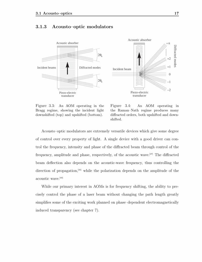
3.1.3 Acousto–optic modulators
xxxxxxxxxxxxxxxxxxxxxxxxxxxxxxxx
xxxxxxxxxxxxxxxxxxxxxxxxxxxxxxxxxxxxxxxxxxxxxxxxxxxxxxxxxxxxxxxxxxxxxxxxxxxxxxxxxxxxxxxxxxxxxxxxxxxxxxxxxxxxxxxxxxxxxxxxxxxxxxxxxxxxxxxxxxxxxxxx
2θΒ
Acoustic absorber
Piezo-electrictransducer
Incident beams Diffracted modes
2θΒ
Figure 3.3: An AOM operating in theBragg regime, showing the incident lightdownshifted (top) and upshifted (bottom).
xxxxxxxxxxxxxxxxxxxxxxxxxxxxxxxxxxxxxxxxxxxxxxxxxxxxxx
xxxxxxxxxxxxxx
0
+1
−1
+2
−2
+nAcoustic absorber
Piezo-electrictransducer
Incident beam
Diffracted m
odes
Figure 3.4: An AOM operating inthe Raman–Nath regime produces manydiffracted orders, both upshifted and down-shifted.
Acousto–optic modulators are extremely versatile devices which give some degree
of control over every property of light. A single device with a good driver can con-
trol the frequency, intensity and phase of the diffracted beam through control of the
frequency, amplitude and phase, respectively, of the acoustic wave.[37] The diffracted
beam deflection also depends on the acoustic-wave frequency, thus controlling the
direction of propagation,[35] while the polarization depends on the amplitude of the
acoustic wave.[40]
While our primary interest in AOMs is for frequency shifting, the ability to pre-
cisely control the phase of a laser beam without changing the path length greatly
simplifies some of the exciting work planned on phase–dependent electromagnetically
induced transparency (see chapter 7).

3.2 AOM driver 18
Our acousto–optic modulator
After careful consideration of the available models, the decision was made to purchase
an IntraAction ATM–200–1A1,[41] with a tellurium dioxide (TeO2) crystal providing
the acousto-optic medium and a lithium niobate (LiNbO3) piezo-electric transducer
used to generate the radio–frequency (RF) acoustic travelling wave. The TeO2 crystal
is coated with a multi-layer dielectric anti-reflection coating, effective across the whole
visible spectrum. See table 3.1 for full details.[42]
Table 3.1: Specifications of the IntraAction ATM–200–1A1 AOM
AOM Specifications
Parameter Condition Value Units
Centre frequency – 200 MHz
Tuning range – 100 MHz
Optical wavelength range – 440–700 nm
Diffraction efficiency Max. 85 %
Optical rise time 1 mm beam diameter 151 ns
Active aperture height – 1 mm
Sound velocity – 4260 ms-1
RF drive power Max. 1 W
RF input impedance – 50 Ω
VSWR Centre frequency 1:1.5 –
3.2 AOM driver
A driver is required to provide a stable RF bias to the piezo-electric actuator producing
the acoustic wave. It is instructive to begin with a wish-list defining the qualities of an
ideal AOM driver before considering the physical restrictions, engineering practicalities
and compromises that are an inevitable part of the design process. Our ideal AOM
would have:

3.2 AOM driver 19
• Stable frequency, tunable over the range supported by the AOM
• Narrow bandwidth, minimizes dispersion in the diffracted beam
• Stable amplitude, tunable over the required diffraction efficiency range
• Stable phase, tunable over 360
In the following discussion, we will see how the choices of components and design
parameters affect these characteristics and attempt to optimize them for our purposes.
3.2.1 Design
The basic layout of this design was inspired by the work of V. L. Ryjkov[43] and is
illustrated in figure 3.5. A low–power, tunable RF signal is provided by a voltage–
controlled oscillator, amplitude control is provided by a tunable attenuator, a low
power signal for real-time monitoring is provided through the coupled output of a
directional coupler, while the power to drive the acoustic wave–train is provided by
an RF–amplifier.
attenuatorAmplifierDirectional
coupler
VoltagePhaseshifter
controlledoscillator
Variable
AOMSpectrumanalyzer
Figure 3.5: Schematic diagram of the AOM driver, showing the main components: avoltage controlled oscillator (VCO), a variable attenuator, a variable phase shifter, adirectional coupler and an RF amplifier. A spectrum analyzer can be used to monitorthe frequency and power output.

3.2 AOM driver 20
Circuit design
The quote from IntraAction for our AOM, described in section 3.1.3 included details
of the ME Series Modulator Drivers.[44] We decided not to purchase a driver for several
reasons:
• The specifications do not include amplitude or phase control
• No circuit diagrams are available, complicating any intended modification
• With a footprint of 9 in × 13.25 in, the casing seemed unnecessarily large
• At a cost of US$1125, it seemed unreasonably expensive given the cost of indi-
vidual components
The RF components used were all purchased from Mini–Circuits1 and are described
in section 3.2.3. The voltage controlled oscillator (VCO) requires a tuning voltage of
0–15 V to cover its dynamic range, while the variable attenuator requires a tuning
current of 0–8 mA. The attenuator datasheet specifies a 0–20 mA tuning current,
however the signal was observed to reach its maximum power at around 8 mA.
Initially the intention was to produce a customized version of the IntraAction
driver and a circuit diagram was produced including all relevant RF components
and control electronics. Many problems were encountered due to cross-talk between
different components and subsequent instability; these are described in section 3.2.2.
During a visit to the laboratory of Prof. J. D. D. Martin at the University of
Waterloo, useful discussions included the suggestion to use a modular approach. This
provides significantly improved isolation between components and increased versatility
as different modules can be added and removed at will. Good impedance matching
ensures minimal losses on the transmission lines between the modules.
The diagrams for the VCO and attenuator circuits are illustrated in figure 3.6.
The RF amplifier was purchased as a complete unit with SMA coaxial connectors,
1http://minicircuits.com/, application notes provide a great deal of useful information.

3.2 AOM driver 21
as component level versions did not meet centre–frequency, bandwidth and output–
power requirements.
Attenuator
+15 V
10 kΩ500 Ω
50 Ω
0.1 µF 0.1 µF
RF in
RF out
10 µF
+15 V
10 k
Ω
10 µF47 pF
VCO
RF out
TS921
NTE490
Figure 3.6: Component–level schematic diagram of the voltage–controlled oscillator(VCO) and variable attenuator circuits used in the AOM driver.
3.2.2 RF issues
While the laws of physics remain the same at all frequencies, the circuit techniques em-
ployed at high frequencies are often radically different to the familiar DC techniques,
as effects such as junction capacitance, wiring inductance and signal wavelength begin
to dominate circuit behaviour.

3.2 AOM driver 22
Electromagnetic interference
Long wires and printed circuit board (PCB) traces act as antennae, generating and re-
ceiving electromagnetic interference. Shielded enclosures, grounded internal partitions
between circuit elements, PCB ground planes and shielded transmission lines all help
to reduce electromagnetic coupling which can distort and attenuate high frequency
signals.[45]
Shielding used in and around RF circuits works on the same principle as a Faraday
cage; free charges in the shielding material are constantly redistributed to cancel any
stray electric fields, either external or generated by a nearby section of the circuit.
Grounding
At radio frequencies, solid grounding is essential; stray inductances can lead to high
impedance on a return line resulting in floating grounds at different potentials in
different sections of a circuit. Internal shielding must be soldered along its entire
length, and partitions and covers require many screws to maintain a good chassis
ground.
A potential difference between two points supposedly held at ground can lead to
ground loops. This can be particularly problematic for RF circuits, causing spurious
signals due to return line oscillations and coupling to and from conductors expected
to carry only DC signals. The grounded shielding described in Electromagnetic
interference, section 3.2.2, can provide paths for ground loops. A separate connec-
tion to the common ground terminal is provided for each RF component to minimize
current flow through the casing.

3.2 AOM driver 23
Skin depth
At high frequencies, current tends to be restricted to regions near the surface of a
conductor; a phenomenon known as the skin effect. From Maxwell’s equations for a
linear, conducting medium, we have,
∇.E =ρ
ε0, (3.8)
∇×E = −∂B∂t, (3.9)
∇.B = 0, (3.10)
∇× B = µ0ε0∂E
∂t+ µ0J, (3.11)
where, for a non–magnetic conductor, the bound charge and polarization currents are
negligible compared with the free charge current, giving a total current density
J ≈ σE. (3.12)
Using the vector identity,
∇×∇× A = ∇(∇.A)−∇2A, (3.13)
and noting that the gradient of the charge density, ρ, is zero in a conductor, we can
obtain the wave equation for the electric field in a conducting medium,
∇2E = µ0ε0∂2E
∂t2+ µ0σ
∂E
∂t. (3.14)

3.2 AOM driver 24
There is a plane wave solution to the wave equation given, for a wave propagating in
the positive z–direction, by
E(z, t) = E0ei(kz−ωt), (3.15)
with a complex wavenumber,
k = kR + ikI , (3.16)
which leads to an exponential decrease in electric field amplitude as the field penetrates
the conductor,
E(z, t) = E0e−kIzei(kRz−ωt). (3.17)
The skin depth d is the characteristic length of the exponential decay,
d =1
kI, (3.18)
where kI comes from the solution to equation 3.14,
kI = ω
√ε0µ0
2
⎡⎣√
1 +
(σ
ε0ω
)2
− 1
⎤⎦
1/2
. (3.19)
For good conductors such as the annealed copper used for the internal wires in the
AOM driver, we can simplify equation 3.19 and substitute it into equation 3.18 to
give:[46]
d ≈√
2
µ0σω. (3.20)

3.2 AOM driver 25
Inserting the values for the conductivity (σ ≈ 60 MSm−1 ) and permeability (µ ≈ µ0)
of copper, along with the centre frequency of the AOM (200 MHz) we obtain a skin
depth d ≈ 4.6 µm. For wires with a diameter D much greater than the skin depth,
the AC resistance is equal to that of a hollow cylindrical conductor with the same
outer diameter and with thickness d,
RAC ≈ ρL
πd(D − d)≈ ρL
πdD. (3.21)
The multi–core wire that was used consisted of seven circular cross–section con-
ductors with a combined area of 0.22 mm2, and has an effective area approximately
2.6 times larger than a solid conductor of equivalent cross–sectional area.
Transmission lines
An RF transmission line consists of two conductors (with one held at RF ground)
separated by a dielectric; the two most common geometries are twisted pair and
coaxial, and each has its own specific characteristics. Two of the key attributes
determining the behaviour of a transmission line are the capacitance per unit length
C and the inductance per unit length L. The characteristic impedance is given by,
Z0 =
√LC . (3.22)
To elucidate the effect of a given characteristic impedance between a source and
a load, we will consider a model system composed of an RF voltage source with
impedance ZS = 50 Ω, a twisted pair transmission line with characteristic impedance
Z0 = 100 Ω and a resistive load with impedance ZL = 50 Ω; the system is illustrated
in figure 3.7.
For a twisted pair transmission line (see figure 3.8) the relevant attributes can be
calculated using the following equations,[47]

3.2 AOM driver 26
= 50 ΩZL
L
= 50 ΩZS = 100 ΩZ0
φ1
φ2
φ1'
Figure 3.7: A model RF circuit with source impedance ZS, a twisted pair transmissionline of length L and characteristic impedance Z0 and a resistive load with impedanceZL. The phase of the RF travelling wave has been labelled as it enters the transmissionline (φ1), on reflection from the load junction (φ2) and on its return to the sourcejunction (φ′
1).
s
dconductorsinsulation
Figure 3.8: Geometryof a twisted pair trans-mission line.
L =µ0
πcosh−1
(sd
)(3.23)
C =πε0εr
cosh−1(sd
) (3.24)
⇒ Z0 =cµ0
π√εr
cosh−1(sd
)(3.25)
Using these values, the velocity factor VF = v/c can be calculated,
VF =1
c√LC
=1√εr. (3.26)
Note that for our model system there is an impedance mismatch at both ends of
the transmission which will lead to partial reflection of the RF signal. This can be
expressed quantitatively in terms of the voltage standing wave ratio (VSWR). The

3.2 AOM driver 27
interference of the incident and reflected signals produces a standing wave; the VSWR
is the ratio of the net voltage amplitude at a maximum to the net amplitude at an
adjacent minimum.
We can define a complex reflection coefficient which is the voltage ratio of the
reflected Vr and incident Vi waves:
Γ =Vr
Vi
=|Vr||Vi|
ej(φr−φi) (3.27)
It is instructive to examine the behaviour of the signal at a termination for three cases
in which Γ is entirely real, and in the general case:
• Open circuit (ZL = ∞): Γ = 1, maximum reflected amplitude, no phase shift
• Matched impedance (ZL = Z0): Γ = 0, no reflection
• Short circuit (ZL = 0): Γ = -1, maximum reflected amplitude, π phase shift
• General case: reflected amplitude |Vr| = |Vi||Γ|, phase shift φr = φi + φΓ
In order to calculate the VSWR we need the voltage amplitude at a maximum VMAX
and an adjacent minimum VMIN ,
VMAX = Vi + Vr = Vi(1 + |Γ|),
VMIN = Vi − Vr = Vi(1 − |Γ|),
⇒ V SWR =1 + |Γ|1 − |Γ| . (3.28)
A high VSWR leads to high RF losses due to the finite resistance of the transmission
line. Multiple reflections effectively increase the length of the transmission line; there

3.2 AOM driver 28
is energy stored in the standing wave in addition to the transmitted power. A matched
impedance minimizes these losses and therefore maximizes the power dissipated in the
load.
The model system was constructed using a Mini–Circuits POS–300 VCO as the
source (output impedance 50 Ω, nominal output power 9.5 mW at 200 MHz) and a
Hameg HM5012-2 spectrum analyzer as the load (input impedance 50 Ω) connected
by a length of homemade twisted pair cable (εr ≈ 2.8 ⇒ Z0 ≈ 100 Ω, see equation
3.25). As the length L of the transmission line is varied we expect the power supplied
to the spectrum analyzer to oscillate as we pass through maxima and minima, see
figure 3.9.[29]
0 50 100 150 200 250 3002
4
6
8
10
Length cm
Tra
nsm
itted
pow
erm
W
Twisted pair transmission line
Figure 3.9: An analysis of power transmitted by a twisted pair transmission line ofvarying length, with a 9.5 mW source at 200 MHz and a 50 Ω load.
The maxima in the power transmission occur when the incident and reflected
waves interfere constructively (φ′1 − φ1 = 2mπ where m is an integer, see figure 3.7).
3.2 AOM driver 29
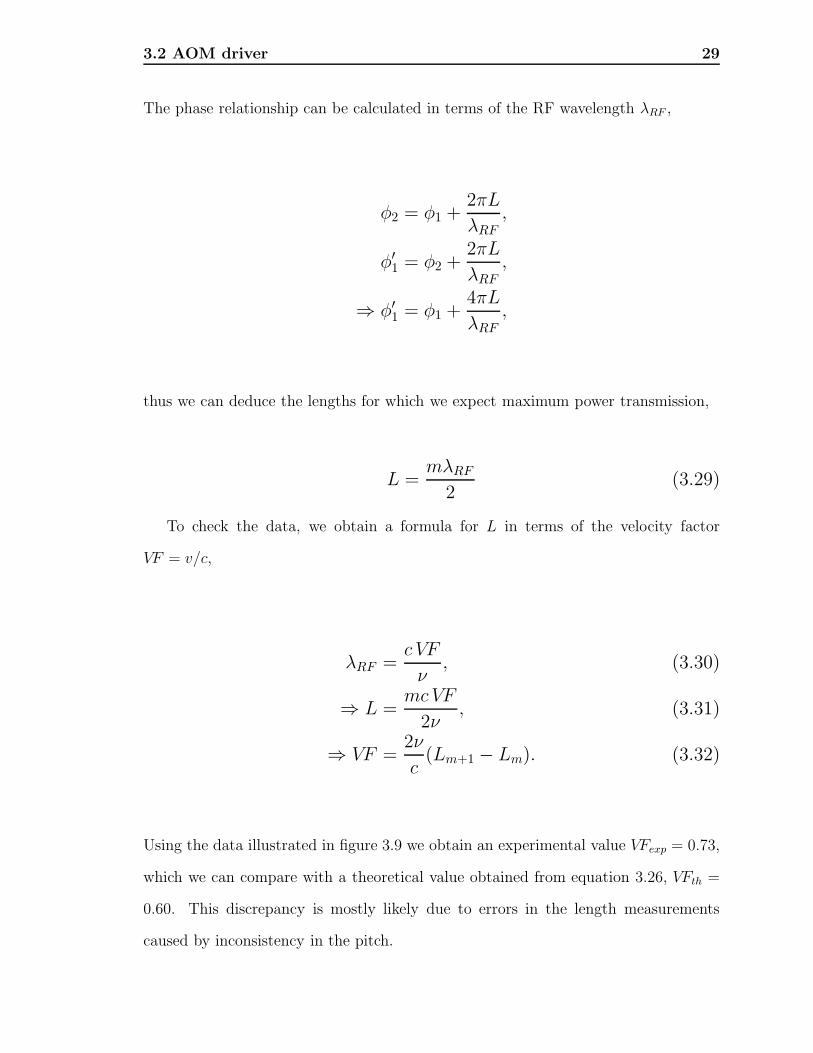
The phase relationship can be calculated in terms of the RF wavelength λRF ,
φ2 = φ1 +2πL
λRF,
φ′1 = φ2 +2πL
λRF,
⇒ φ′1 = φ1 +4πL
λRF,
thus we can deduce the lengths for which we expect maximum power transmission,
L =mλRF
2(3.29)
To check the data, we obtain a formula for L in terms of the velocity factor
VF = v/c,
λRF =c VF
ν, (3.30)
⇒ L =mcVF
2ν, (3.31)
⇒ VF =2ν
c(Lm+1 − Lm). (3.32)
Using the data illustrated in figure 3.9 we obtain an experimental value VFexp = 0.73,
which we can compare with a theoretical value obtained from equation 3.26, VFth =
0.60. This discrepancy is mostly likely due to errors in the length measurements
caused by inconsistency in the pitch.

3.2 AOM driver 30
Decoupling capacitors
In precision RF circuits, liberal use of decoupling capacitors can significantly improve
performance; two types of capacitor are used in the AOM driver circuits for this
purpose.
• Ceramic disk capacitors are suitable for high frequency signals. 47 pF ceramic
disk capacitors are used to provide a path to ground for any stray RF signals
that might otherwise couple into a DC section of the circuit.
• Electrolytic capacitors are available with high values, but have poor high fre-
quency characteristics. 10 µF electrolytic capacitors are used to provide a path
to ground for power line fluctuations which would otherwise cause instability in
the control electronics for the VCO and attenuator.
3.2.3 Construction
The modular design of the system greatly simplified construction, allowing individual
sub–systems to be tested individually using a basic VCO circuit as a high frequency
signal generator and monitoring the output on a spectrum analyzer.
Components
Table 3.2: List of Mini-Circuits RF components for the AOM driver.
AOM driver components
Component Model Characteristic Range
Voltage–controlled oscillator POS–300 Output frequency 150 → 280 MHz
Variable attenuator PAS–1 Signal attenuation 3.6 → 50 dB
Variable phase shifter ELS–450 Phase shift 0 → 360
Directional coupler PDC–20–3 Mainline loss 0.35 → 0.6 dB
RF amplifier ZFL–1000VH Gain 21.6±0.5 dB

3.2 AOM driver 31
All RF components were sourced from Mini-Circuits due to the author’s prior
familiarity with their range. It should be noted that components from other manu-
facturers may offer equivalent or superior performance.
Printed circuit boards
The printed circuit board (PCB) designs were produced using the EAGLE electronic
design package, an almost fully functional version of which is available free for non–
commercial use.2 EAGLE contains a set of libraries including many commonly–used
electronic devices with associated schematic symbols, and board layouts for specific
models; for specialist components such as the RF devices, a set of tools is provided
to create custom libraries.
One of the key design considerations was provision of appropriate grounding for
each module in the device, thus a ground plane was included that separated all com-
ponents, signal lines and power lines. The PCB layout is shown in figure 3.10.
The completed device
Figure 3.11 shows the completed system. The modular design allows individual sub–
systems to be removed; the minimal required system consists of the VCO to produce
the RF signal, and the RF amplifier to increase the signal amplitude to provide enough
power to drive the piezo–electric actuator within the AOM.
3.2.4 Characterization
Having completed construction of the AOM driver, data was collected to assess the
performance of the device under varying conditions. The tests performed fall into
two categories: electrical tests performed on the driver, and optical tests to assess the
capabilities of the AOM controlled by the driver.
2http://www.cadsoft.de/freeware.htm

3.2 AOM driver 32
Figure 3.10: Diagram illustrating the printed circuit board (PCB) layouts for thevoltage–controlled oscillator (VCO), variable attenuator (Attn) and directional coupler(Coupler) circuits used in the AOM driver. The ground plane has been omitted forclarity.
Electronic testing
The attenuator requires a control current provided through an n-channel FET as
shown in figure 3.6. During testing of how diffraction efficiency depends on RF power
it became clear that the attenuation varies in an extremely non–linear way as the
controlling potentiometer is adjusted. In order to quantify this, measurements were
taken to assess how tuning current and output power vary as the potentiometer is
adjusted; the results are shown in figures 3.12 and 3.13 respectively.
The current source providing the tuning current is extremely linear for the range
2–30 mA; one can conclude that the non–linear change in diffraction efficiency is
due to a non–linear relationship between attenuation and tuning current. It may be
worth attempting to provide a non–linear tuning current in order to “smooth out”
the attenuation curve to some extent.

3.2 AOM driver 33
Figure 3.11: Image of the AOM driver including (from the left) the VCO unit andvariable attenuator (both with control potentiometers), the directional coupler (withlow power coupled output a the base of the image) and the RF amplifier.
Optical testing
An acousto–optic modulator is a device used to control the properties of laser light. As
such, the most important tests are those which determine the effect of the device on a
laser beam passing through the acoustic wave. Optical testing was accomplished using
the light from an external cavity diode laser (ECDL) at 670 nm,[48] and a Coherent
LaserMate–Q laser power meter.
Due to variation in the VCO power output as it is tuned off its centre frequency,
as well as small variations in amplifier gain (less than 0.1 dB over the VCO frequency
range), one expects to see frequency dependent changes in the diffraction efficiency.
Figure 3.14 shows the diffraction efficiency spectrum which remains fairly flat at just
over 50 % within the 150 → 280 MHz range stated in the VCO datasheet.
The variable attenuator is provided to allow direct tuning of the diffraction effi-
ciency and hence provide control over the intensity of the diffracted beam. Figure
3.15 illustrates the dependence of diffraction efficiency on RF power supplied to the

3.2 AOM driver 34
0 5 10 15 200
5
10
15
20
25
30
Potentiometer turns
Tun
ing
curr
ent
mA
Figure 3.12: The current provided by theFET in the attenuator circuit in figure 3.6is linear over most of the range, however theattenuation only varies below 8 mA.
0 5 10 15 200
1
2
3
4
Potentiometer turns
RF
pow
erm
W
Figure 3.13: Tuning the RF power suppliedto the amplifier using the attenuator. Thesteps are caused by the 0.4 dBm resolutionof the spectrum analyzer used to take themeasurements.
AOM. The RF power was monitored from the coupled output and the actual power
delivered was calculated from the specifications of the directional coupler, assuming
18 dB amplifier gain. The stated maximum output power of the amplifier is 25 dBm,
causing the roll off at high power.
150 200 25010
20
30
40
50
Frequency MHz
Dif
frac
tion
effi
cien
cy
Figure 3.14: Establishing the dependenceof diffraction efficiency on acoustic fre-quency for the AOM–driver system, usinga diode laser at 670 nm.
5 10 15 20 250
10
20
30
40
50
Calculated output power dBm
Dif
frac
tion
effi
cien
cy
Figure 3.15: Tuning the diffraction effi-ciency of the AOM–driver system, using thevariable attenuator included in the AOMdriver. Frequency = 200 MHz.

Chapter 4
Real Time Laser Mode Structure
Analysis
One of the many advantages of using lasers as a light source for addressing transitions
in atoms and molecules is their extremely narrow bandwidth. The actual frequencies
emitted by a laser subject to inhomogeneous broadening due to the effects of the
velocity distribution, spatial field inhomogeneities, or the presence of impurities in
the gain medium, are given by the product of the active medium gain profile and the
allowed modes of the laser cavity; see figure 4.1.[49]
=Frequency
Figure 4.1: Diagram illustrating the origin of the observed mode–structure of a typicallaser. The product of the gain profile with the spectrum of allowed cavity modesproduces the characteristic “peaks under a curve” spectrum.
For applications requiring precise frequency control, it is important that the laser
radiation includes only a single longitudinal cavity mode; there are many locking

36
techniques used to achieve this.[50][51][52][53]
As no frequency locking system is totally reliable, it is extremely useful to have
a way of monitoring laser mode structure in real time over the course of an exper-
iment. The typical approach uses an optical spectrum analyzer (OSA) which varies
the separation between a pair of highly reflecting mirrors, arranged as a Fabry–Perot
interferometer, and detects the transmitted intensity from incident laser light. While
this system is simple to use and effective, it is expensive, requires a dedicated oscil-
loscope, and occupies a large footprint, making it impractical to provide one for each
laser system required to operate on a single mode.
Laser
L1 L2
LA LB λ / 2plate
W1
W2
Opticalisolator
Etalon
Imagesensor
OSA
DisplayPIC
SensorPIC
LCD
Figure 4.2: The experimental setup illustrating the optical train which produces theFabry–Perot interference pattern, the digital image sensor used to record the pattern,the microcontrollers which record and reformat the data and the LCD used to displaythe resulting trace. Lenses LA and LB focus the beam through an optical isolatorand subsequently recollimate it. Optical wedges W1 and W2 have approximately 4 %reflectivity at 670 nm, leaving 0.16 % of the initial beam incident on the OSA. LensL1 ensures a high intensity beam illuminates the etalon, while lens L2 both focusesthe individual fringes onto the image sensor, and collimates the beam.
In this chapter, a novel system is presented which has been constructed in our
laboratory with a device cost and footprint which make it realistic to provide one for
4.1 Producing an interference pattern 37
each laser system. A diagram illustrating the concept is shown in figure 4.2. A low
power laser beam, which may be obtained from the back reflection off any uncoated
optical element, incident on a solid etalon produces a spatially varying interference
pattern characteristic of the laser mode structure. The Fabry–Perot pattern illumi-
nates a CMOS digital image sensor, the data is recorded and reformatted by a pair
of programmable microcontrollers and displayed on a component level LCD.
4.1 Producing an interference pattern
A laser beam incident on an etalon at a range of angles produces a stationary inter-
ference pattern. As the pattern is circularly symmetric, all of the information can
be obtained in a radial scan. Accordingly, the image sensor is placed such that the
pattern is vertically aligned with its central row, with the edge of the sensor pixel
array positioned between the centre of the pattern and the first order fringe.
The optical train we have used to obtain the interference pattern is included in
figure 4.2. The laser beam is focused through an optical isolator, a second lens ensures
the resulting beam is parallel. Reflection from a pair of optical wedges reduces the
beam power to approximately 4 µW before it is focused onto the etalon. The beam
has a width d1 = 2.5 mm at lens L1 and a width d2 = (f2/f1)d1 = 8 mm at the image
sensor, which has an active area width of 6.66 mm. The fringe of order p is focused
at the back focal plane of lens L2 with a diameter given by
D2p =
4f 22n
′λn2h
(p− 1 + ε), (4.1)
where λ is the wavelength of the light, h is the thickness of the etalon, f2 is the focal
length of lens L2, n and n′ are the refractive indices outside and inside the etalon
respectively, and ε is the excess fraction.[54] Lens L2 is chosen such that three intensity
peaks can fit within the active width of the image sensor. This ensures that at least

4.2 The image sensor 38
two fringes are always visible, clearly delineating a free spectral range.
4.2 The image sensor
The device used to record the interference pattern is a Micron MT9M001C12STM 1.3
megapixel CMOS digital image sensor,[55] with 1024 rows × 1280 columns (SXGA).
Inputs and outputs are entirely digital, using low power 3.3 V logic. Intensity values
are provided on a 10–bit wide bus (of which 8 bits are used) synchronized with an
external clock source, which must lie within the range 1 to 48 MHz. This clock is
provided by a microcontroller configured to output a clock signal at 1/4 of its 8 MHz
internal clock frequency, giving a sensor clock frequency of 2 MHz.
A commercial digital camera would not give direct access to the digital intensity
values for each pixel, would be challenging to synchronize with a microcontroller due
to the internally generated clock signal, and, in general, would not give direct access
to the windowing capabilities required to read data from a narrow strip across the
sensor array.
A CMOS image sensor consists of a two–dimensional array of photodiodes which
accumulate charge at a rate proportional to the intensity of incident light within a
certain spectral range. The primary difference between a CCD and a CMOS image
sensor lies in the way the charge is read by the associated electronics. CCDs transport
the charge across the chip so that it can be read off pixel–by–pixel using a transistor
placed at a corner of the array. Achieving this without significant distortion requires a
special manufacturing process which is incompatible with the CMOS class of integrated
circuits. A CMOS image sensor has readout transistors integrated into each pixel,
obviating the need for charge transport.[56]
Three major practical advantages of a CMOS image sensor over a CCD are the low
power consumption due to simpler control electronics, low cost due to the ubiquity of
4.2 The image sensor 39
the CMOS manufacturing process, and easy integration of ADC allowing CMOS sensors
to give a digital output. CCDs can have a higher resolution as the entire active area
consists of a photodiode array without the need for the associated readout transistors.
The requirement for a digital output that can be read directly by a microcontroller
proved to be the decisive factor in choosing a CMOS image sensor over a CCD.
4.2.1 Configuration settings
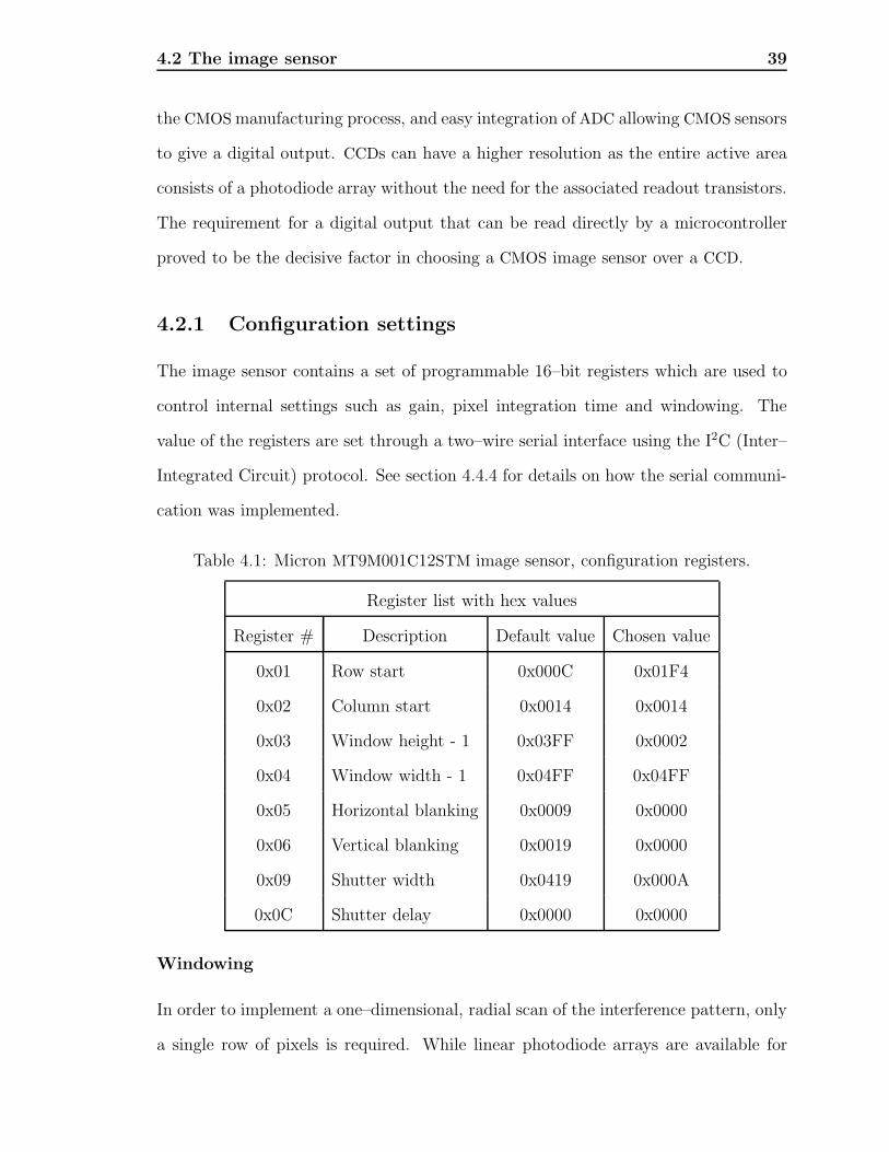
The image sensor contains a set of programmable 16–bit registers which are used to
control internal settings such as gain, pixel integration time and windowing. The
value of the registers are set through a two–wire serial interface using the I2C (Inter–
Integrated Circuit) protocol. See section 4.4.4 for details on how the serial communi-
cation was implemented.
Table 4.1: Micron MT9M001C12STM image sensor, configuration registers.
Register list with hex values
Register # Description Default value Chosen value
0x01 Row start 0x000C 0x01F4
0x02 Column start 0x0014 0x0014
0x03 Window height - 1 0x03FF 0x0002
0x04 Window width - 1 0x04FF 0x04FF
0x05 Horizontal blanking 0x0009 0x0000
0x06 Vertical blanking 0x0019 0x0000
0x09 Shutter width 0x0419 0x000A
0x0C Shutter delay 0x0000 0x0000
Windowing
In order to implement a one–dimensional, radial scan of the interference pattern, only
a single row of pixels is required. While linear photodiode arrays are available for

4.2 The image sensor 40
specialist applications in spectroscopy, two–dimensional arrays used for photographic
applications are inexpensive and widely available with a resolution higher than any
linear array found to date. In order to use a two–dimensional image sensor, the active
window is set to span the entire 6.66 mm active width, using the minimum height of
just three rows. With a pixel spacing of 5.2 µm in both the horizontal and vertical
directions, the effects of fringe curvature should be minimal.
Four registers control the window position and dimensions, setting the first row,
first column, window height and window width. The first column and window width
parameters are left as their default values, ensuring the entire width of the pixel array
is utilized. The first row to be read is number 500 (hex value 0x01F4), approximately
half way down the array; a value of two (0x0002) in the third register selects the three
row window height.
Blanking
In addition to the region of optically black pixels surrounding the active area, the
image sensor has the capability to blank a specified number of pixels at the beginning
of each row (horizontal blanking) and a specified number of rows at the end of each
frame (vertical blanking), to allow the active area to be changed without altering
the dimensions of the pixel array, or the pixel integration time. The sensor outputs
LINE VALID and FRAME VALID signals which remain low during horizontal and
vertical blanking respectively.
The total frame time includes the time spent in the blanked regions; this overides
previous window settings. The horizontal and vertical blanking registers have both
been set to zero to maximize the frame rate, giving maximum flexibility in the display
refresh rate.

4.2 The image sensor 41
Pixel integration time
The pixel sensitivity can be controlled by adjusting the period during which charge
is accumulated in the photodiodes prior to readout; the period tINT is specified as a
number of sensor clock periods,
tINT = (Reg0x09 × row time) − overhead time − reset delay, (4.2)
where
row time = [(Reg0x04 + 1) + 244 + Reg0x05 − 19] × τCLK,
overhead time = 180 × τCLK,
reset delay = 4 × Reg0x0C × τCLK .
The default shutter width 0x0419 (1049 lines) allows charge to accumulate for a
full frame period giving maximum sensitivity. The shutter width is reduced to 0x000C
(12 lines, tINT = 7.55 ms) matching the sensitivity to the incident laser power and
avoiding saturation due to ambient light.
4.2.2 Image sensor characterization
An experiment was performed to assess the variation in pixel sensitivity across the
active width of the sensor. The program implemented on the microcontrollers was
modified to record the maximum intensity detected by each pixel (see Program
extensions, section 4.4.4 for details); a flashlight incident on a 300 µm circular
aperture was used as a constant intensity light source while the sensor was translated
through the beam. The fractional variation (σn−1/〈I〉) in the intensity I was found
to be 1.4 %.

4.2 The image sensor 42
4.2.3 The image sensor circuit
Figure 4.3: Schematic diagram of the image sensor circuit including the sensor, a ZIFconnector for a 20–contact ribbon cable along with capacitors for signal conditioning.The “/” symbol denotes a signal which produces its effect during a logic zero.
The image sensor is housed in a 48–pin plastic leadless chip carrier (PLCC), a
square surface mount package with twelve contacts along each side. Rather than
soldering directly on to the board, a through–hole socket1 was purchased, greatly
simplifying board assembly and sensor replacement.
The sensor circuit includes a number of decoupling capacitors to reduce noise on
the various signal lines and a 20–contact, vertical, zero insertion force (ZIF) connector
1Loranger International Corporation, part number 04440 481 X215.

4.3 The display 43
for a 1 mm pitch ribbon cable used to transmit the signal lines to the main system
board. The circuit diagram is shown in figure 4.3, while the layout of the board is
depicted in figure 4.4.
The ribbon cable includes a 10–bit wide bus for the intensity data, of which only
the eight most significant bits are used. The microcontroller inputs and outputs are
arranged as 8–bit ports which can be addressed in a bytewise fashion (See section
4.4.3); obtaining the full 10–bit resolution would require a disproportionate increase
in processing time. See section 4.6 for discussion of possible improvements to this
system.
4.3 The display
The LCD used to display the mode structure information is an Optrex F–51477GNB–
FW–AD with 240 rows × 320 columns. In order to produce a plot of intensity as a
function of position on the image sensor, data points must be plotted consecutively
according to their x–values; as the display must be written to sequentially by row,
the display is rotated such that the y–axis, representing the intensity values, is the
long axis. The 8–bit resolution of the intensity data leads to a dynamic range of 256
on the y–axis, similar to many commercial oscilloscope displays.
Every fifth sensor pixel is represented by a corresponding row on the display, such
that the 240 rows of the display represents the width covered by 1200 out of the 1280
pixels spanning the active region of the sensor. The row position corresponds to the
position of the sensor pixel; a marker is placed on each row such that the top of the
marker indicates the intensity value and the length is set to ensure a continuous curve;
see section 4.4.4.

4.3 The display 44
Figure 4.4: Layout of the printed circuit board housing the image sensor and a 20conductor, 1 mm pitch, vertical ZIF connector along with a resistor and capacitorsfor signal conditioning.
4.3.1 Timing
The finite rise and decay times of the LCD pixels place significant constraints on the
frame refresh rate and lead to variation in the apparent contrast with frame period.
A variable delay is implemented after each row is written with real time control to
permit user optimization. In order to objectively assess the optimum frame period, a
photodiode was used to record light intensity from the centre of the display.
Figure 4.5 illustrates the complex nature of the variation in display intensity.
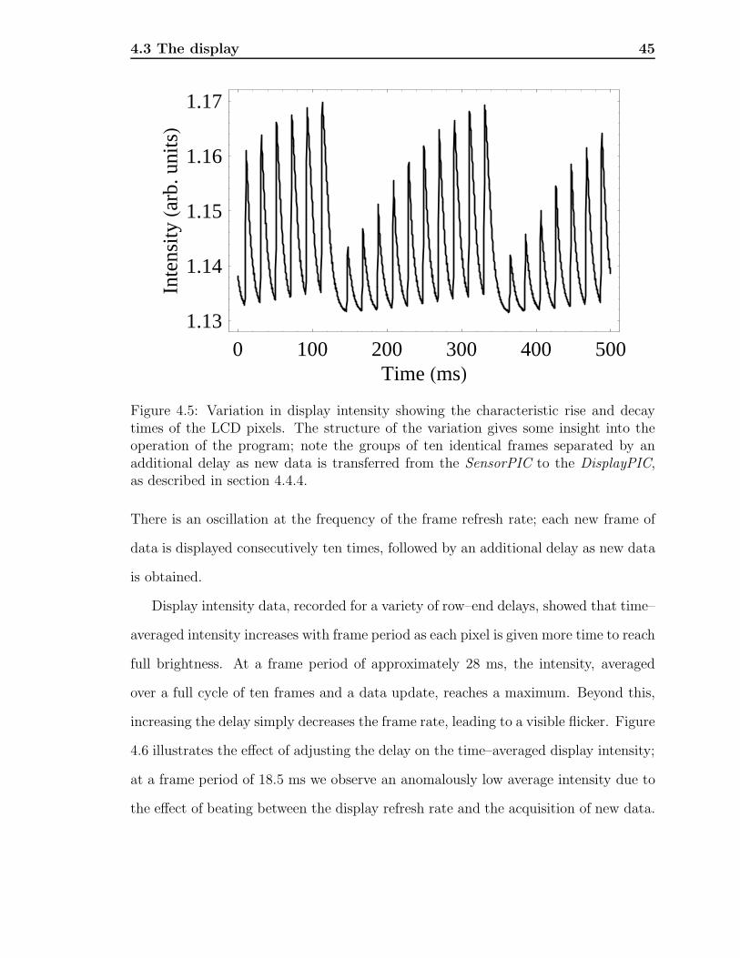
4.3 The display 45
0 100 200 300 400 500Time ms
1.13
1.14
1.15
1.16
1.17
Inte
nsitya
rb.u
nits
Figure 4.5: Variation in display intensity showing the characteristic rise and decaytimes of the LCD pixels. The structure of the variation gives some insight into theoperation of the program; note the groups of ten identical frames separated by anadditional delay as new data is transferred from the SensorPIC to the DisplayPIC,as described in section 4.4.4.
There is an oscillation at the frequency of the frame refresh rate; each new frame of
data is displayed consecutively ten times, followed by an additional delay as new data
is obtained.
Display intensity data, recorded for a variety of row–end delays, showed that time–
averaged intensity increases with frame period as each pixel is given more time to reach
full brightness. At a frame period of approximately 28 ms, the intensity, averaged
over a full cycle of ten frames and a data update, reaches a maximum. Beyond this,
increasing the delay simply decreases the frame rate, leading to a visible flicker. Figure
4.6 illustrates the effect of adjusting the delay on the time–averaged display intensity;
at a frame period of 18.5 ms we observe an anomalously low average intensity due to
the effect of beating between the display refresh rate and the acquisition of new data.

4.4 The microcontrollers 46
15 20 25 30 35 40 451.12
1.13
1.14
1.15
1.16
Frame Period ms
Ave
rage
Inte
nsitya
rb.u
nits
Figure 4.6: Average intensity increases with row–end delay, reaching a maximum atapproximately 28 ms. Note the anomalous value at a delay of 20.5 ms due to beatingbetween the frame refresh rate and the frequency of data updates by the DisplayPIC.
4.4 The microcontrollers
To achieve the precise control of multiple complex devices at the speeds required, low
cost microcontrollers from the PICMicro R© family were employed. The final design
utilized two different microcontrollers; one used to control the sensor (subsequently
referred to as the SensorPIC) and the other used to control the LCD (subsequently
referred to as the DisplayPIC).[57]
SensorPIC
• Model PIC18LF2320 operating on the 3.3 V logic required by the sensor
• Configures sensor prior to system operation
• Provides 2 MHz clock signal used to synchronize output of intensity data
• Reads and stores a full frame of intensity data
• Makes intensity data available to DisplayPIC on request
DisplayPIC
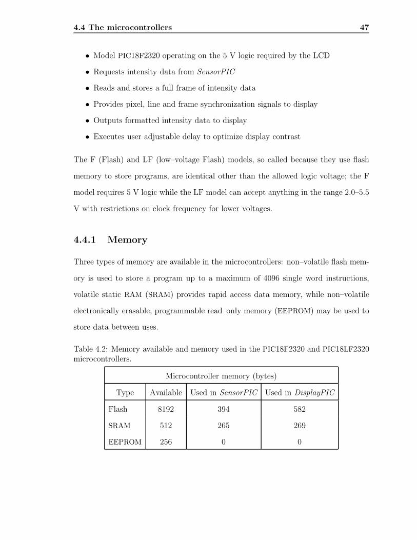
4.4 The microcontrollers 47
• Model PIC18F2320 operating on the 5 V logic required by the LCD
• Requests intensity data from SensorPIC
• Reads and stores a full frame of intensity data
• Provides pixel, line and frame synchronization signals to display
• Outputs formatted intensity data to display
• Executes user adjustable delay to optimize display contrast
The F (Flash) and LF (low–voltage Flash) models, so called because they use flash
memory to store programs, are identical other than the allowed logic voltage; the F
model requires 5 V logic while the LF model can accept anything in the range 2.0–5.5
V with restrictions on clock frequency for lower voltages.
4.4.1 Memory
Three types of memory are available in the microcontrollers: non–volatile flash mem-
ory is used to store a program up to a maximum of 4096 single word instructions,
volatile static RAM (SRAM) provides rapid access data memory, while non–volatile
electronically erasable, programmable read–only memory (EEPROM) may be used to
store data between uses.
Table 4.2: Memory available and memory used in the PIC18F2320 and PIC18LF2320microcontrollers.
Microcontroller memory (bytes)
Type Available Used in SensorPIC Used in DisplayPIC
Flash 8192 394 582
SRAM 512 265 269
EEPROM 256 0 0

4.4 The microcontrollers 48
Flash memory
The user program, created in assembly language and compiled into hexadecimal for-
mat, is ultimately stored in binary form in the microcontroller program memory,
implemented in Flash. Flash memory is readable, writable and erasable during op-
eration; a read is executed in blocks of a single byte, a write is executed in blocks
of 8 bytes, while an erase operation occurs in blocks of 64 bytes and cannot be im-
plemented in user code. This architecture makes it possible, but impractical, to use
program memory for storing data.
Note that the programs implemented in the SensorPIC and DisplayPIC use ap-
proximately 5 and 7 % respectively of the available program memory, giving plenty
of scope for program extensions. See section 4.4.4 for further discussion of this.
Static RAM
High speed, volatile data memory is implemented as static RAM with 12–bit register
addresses used to store special function registers (SFR) and general purpose registers
(GPR). SFRs control specific functions of the device; for example, bits 6–4 of the OSC-
CON register set the frequency of the internal oscillator, used in the SensorPIC. GPRs
are used for data storage in user applications; examples include the Time counters
used to implement delays and the LineCount variable used to determine which LCD
row is currently being addressed.
Data memory may be addressed directly or indirectly. Direct addressing has been
used to reset counters to their initial values; in such cases the location of the register
must be specified. An SFR called the Bank Select Register can be used to determine
the data memory bank in which the register is stored; alternatively, a feature called
the Access Bank can be used, providing access to limited sections of the data mem-
ory using 8–bit addresses. We have used the Access Bank for all direct addressing
operations.

4.4 The microcontrollers 49
Indirect addressing of data memory does not specify a particular register address,
rather it uses a set of SFRs to keep track of, write to and read from an abstract
table. The File Select Register for the nth table (FSRn) points to the current register,
while writing to or reading from INDFn writes to or reads from the register currently
selected by FSRn. The use of POSTINCn, PREINCn, POSTDECn and PREDECn
works in the same manner as INDFn with an increment or decrement of FSRn, either
before or after the operation. Indirect addressing is used to store the table of 240
8–bit intensity values which together constitute a single frame of data to be displayed
on the LCD.
EEPROM
The inclusion of EEPROM allows user data to be stored while the device is unpowered.
Currently this is not being exploited, however it is interesting to note that the 256
bytes available provide enough memory to store a full frame of 240 intensity values,
allowing for the inclusion of a “frame save” feature. This is discussed further in section
4.4.4.
4.4.2 Clocking
One of the benefits of PIC microcontrollers is the precise temporal control they afford
the user. A variety of clock sources can be used giving a known clock cycle period;
each single word instruction takes exactly four clock cycles to execute.
SensorPIC: internal RC oscillator
Oscillator selection is achieved using the configuration register CONFIG1H; one of a
set of registers stored in the dedicated configuration memory space described in Flash
memory, section 4.4.1. Bits 3–0 → 1001 selects the internal RC oscillator with pin
6 of port A (RA6, see section 4.4.3) configured to provide a square wave output at

4.4 The microcontrollers 50
a quarter of the internal oscillator frequency. This is the only special function pin
exploited in the SensorPIC and it is used to provide the clock signal for the image
sensor.
The internal RC oscillator has a selectable frequency of 2n× 125 kHz, where n is
an integer between 0 and 6, giving a maximum frequency of 8 MHz, selected using
the OSCCON SFR (see section 4.4.1).
DisplayPIC: high speed crystal oscillator with phase–locked loop
Timing is critical when driving an LCD as the finite rise and fall times of the pixels
produce a limited window for the frame refresh rate outside of which no image is
visible, see section 4.3.1. To provide maximum flexibility in the frame refresh rate,
the DisplayPIC had to run at the maximum achievable frequency.
Again configuration register CONFIG1H is used to select the oscillator mode:
bits 3–0 → 0110 select a high speed crystal oscillator with the phase–locked loop
(PLL) function enabled. The oscillator used is a CTS Reeves MP101 parallel crystal
which resonates at 10 MHz, while the PLL increases the frequency by a factor of four
using an internal voltage controlled oscillator, with a secondary output reduced in
frequency by a factor of four and phase–locked to the crystal oscillator output using
a phase comparator in a negative feedback loop.[58]
High speed crystal oscillators up to 20 MHz may be used without the PLL, however
the maximum frequency obtainable uses a 10 MHz crystal, producing a phase–locked
loop output signal at 40 MHz. A stable supply voltage is essential in this clocking
mode; a 10 µF electrolytic capacitor between VCC and ground helps to ensure stable
oscillation.
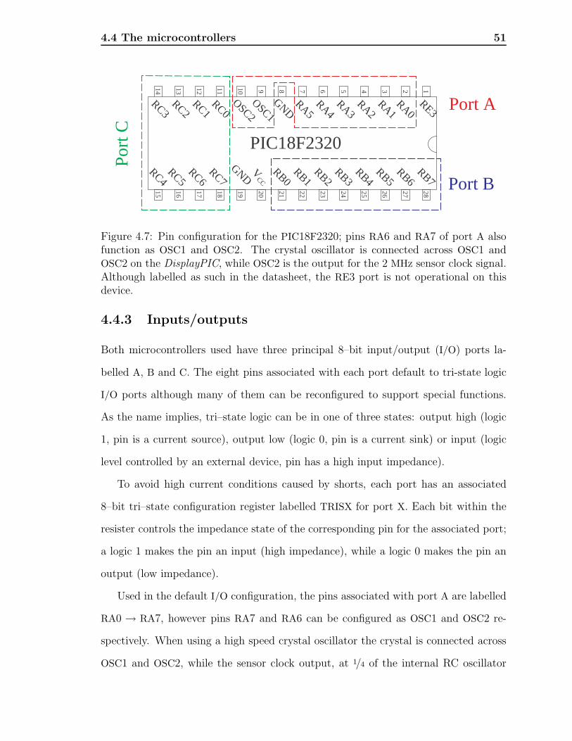
4.4 The microcontrollers 51
PIC18F2320
RC0RC1
RC2OSC1
OSC2
1234567891011121314
GNDRA0
RA1RA2
RA3RA4
RA5RE3
1918171615 2423222120 28272625
RC3
RC7RC6
RC5V
CC
RB0RB1
RB2RB3
RB4RB5
RC4GND
RB6RB7 Port B
Port APo
rt C
Figure 4.7: Pin configuration for the PIC18F2320; pins RA6 and RA7 of port A alsofunction as OSC1 and OSC2. The crystal oscillator is connected across OSC1 andOSC2 on the DisplayPIC, while OSC2 is the output for the 2 MHz sensor clock signal.Although labelled as such in the datasheet, the RE3 port is not operational on thisdevice.
4.4.3 Inputs/outputs
Both microcontrollers used have three principal 8–bit input/output (I/O) ports la-
belled A, B and C. The eight pins associated with each port default to tri-state logic
I/O ports although many of them can be reconfigured to support special functions.
As the name implies, tri–state logic can be in one of three states: output high (logic
1, pin is a current source), output low (logic 0, pin is a current sink) or input (logic
level controlled by an external device, pin has a high input impedance).
To avoid high current conditions caused by shorts, each port has an associated
8–bit tri–state configuration register labelled TRISX for port X. Each bit within the
resister controls the impedance state of the corresponding pin for the associated port;
a logic 1 makes the pin an input (high impedance), while a logic 0 makes the pin an
output (low impedance).
Used in the default I/O configuration, the pins associated with port A are labelled
RA0 → RA7, however pins RA7 and RA6 can be configured as OSC1 and OSC2 re-
spectively. When using a high speed crystal oscillator the crystal is connected across
OSC1 and OSC2, while the sensor clock output, at 1/4 of the internal RC oscillator

4.4 The microcontrollers 52
frequency, is provided from OSC2.
4.4.4 The program
The program consists of two processes running separately on the two microcontrollers.
The SensorPIC starts by configuring the image sensor, then reads a frame of intensity
data and transfers the data to the DisplayPIC using a custom communication protocol.
The DisplayPIC receives the frame of intensity data, then plots the resulting curve
on the display. The program is illustrated in schematic form in figure 4.8.
Configuring the sensor
The PIC18LF2320 microcontroller used to communicate with the sensor has a built–
in serial communications module called the Master Synchronous Serial Port (MSSP),
with I2C capability. Serial programming using the MSSP is an extremely simple auto-
mated process; unfortunately, hardware limitations necessitated a more complicated,
low–level approach.
The two pins used to provide the serial clock (SCLK) and serial data (SDATA)
signals are part of digital I/O port C, one of just three ports available. The master
clock for the sensor is provided from a pin which would otherwise form part of port A.
As we need one full port to receive data from the image sensor and another to output
the reformatted data with the correct timing, we can only use special function pins
from a single port, thus a subroutine was constructed within the assembly code (see
appendix A) to allow serial communication using two general I/O pins.
Reading data from the sensor
Reading intensity data from the sensor commences when the 8–bit value representing
the intensity detected by the first pixel in a row becomes available on the SensorPIC
input data bus; this is synchronized with the rising edge of the LINE VALID signal
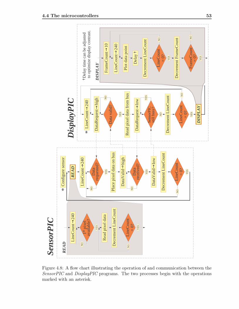
4.4 The microcontrollers 53
RE
AD
Dat
are
ques
ted?
NO
YE
S
Dat
are
ceiv
ed?
YE
S
Dat
a va
lid?
NO
YE
S
YE
S
DIS
PL
AY
NO
Lin
eCou
nt
240
Dec
rem
ent L
ineC
ount
Lin
eCou
nt=
0?
YE
S
NO
Dec
rem
ent L
ineC
ount
Lin
eCou
nt=
0?
YE
S
NO
Con
figu
re s
enso
r
Lin
eCou
nt
240
1st p
ixel
avai
labl
e?
YE
S
NO
Rea
d pi
xel d
ata
Dec
rem
ent L
ineC
ount
Lin
eCou
nt=
0?
YE
S
NO
RE
AD
Lin
eCou
nt
240
Fram
eCou
nt
10
Lin
eCou
nt
240
Plot
dat
a po
int
Del
ay
Dec
rem
ent L
ineC
ount
Lin
eCou
nt=
0?
YE
S
NO
Dec
rem
ent F
ram
eCou
nt
Fram
eCou
nt=
0?
YE
S
NO
DIS
PL
AY
Del
ay ti
me
can
be a
djus
ted
to
optim
ize
disp
lay
cont
rast
.
Sens
orP
IC
Dis
play
PIC
Plac
e pi
xel d
ata
on b
us
Dat
aVal
id
hig
h
Dat
aVal
id
low
Dat
aReq
uest
h
igh
Rea
d pi
xel d
ata
from
bus
Dat
aReq
uest
lo
w
Sens
orPI
Cst
ill b
usy?
NO
*
*
Figure 4.8: A flow chart illustrating the operation of and communication between theSensorPIC and DisplayPIC programs. The two processes begin with the operationsmarked with an asterisk.

4.4 The microcontrollers 54
from the sensor. Following this, the full frame of 240 values is read using a program
loop composed of five instruction cycles; as each instruction cycle corresponds to a
single cycle of the clock signal sent to the sensor, every fifth pixel intensity value is
recorded. Thus the actual sensing width covers 240 × 5 = 1200 out of a total 1280
pixels across the active width of the sensor.
The full frame of data is stored using the indirect addressing approach described
in section 4.4.1; each value is written to the POSTINC0 register, which subsequently
transfers it into the register indicated by FSR0, then increments the value of FSR0.
The LineCount variable, initially given a value of 240, is decremented after each value
is read and the sequence is terminated once it reaches zero.
Data transfer
Due to the different requirements of their respective peripherals, the two microcon-
trollers run at different clock speeds; a custom protocol was implemented to facilitate
communication and ensure that no data is lost. The system uses two control lines
and an 8–bit data bus: the data request line is set high by the DisplayPIC to indicate
that it is ready to receive a byte of intensity data, the data valid line is subsequently
set high by the SensorPIC to indicate that a valid byte of data is available on the
data bus. The DisplayPIC sets the data request line low to indicate that the data has
been received and stored, and, finally, the SensorPIC sets the data valid line low to
ensure that the same value is not retransmitted on the next data request.
Writing to the display
Upon receipt of each data valid signal, the DisplayPIC transfers a single byte of
intensity data from the data bus into a table using the same indirect addressing
system described in section 4.4.1. Once a full frame of 240 values has been stored,
the display algorithm can begin.

4.4 The microcontrollers 55
The display is initialized by switching on the 5 V input to the voltage regulator
supplying the 1.7 V power source for the LCD Drive and setting the DISPOFF signal
high. A set of coordination signals are used to synchronize the writing operation:
the data latch signal, LP, is used to indicate the start of a new row and the first
line marker, FLM, is used to indicate the start of a new frame. The display clock
signal, CP, is provided only as needed from a general I/O pin, and consequently has
no defined duty cycle.
For convenience, while dealing with the coordination signals, the first line is written
entirely as zeros, corresponding to bright pixels. Each following line includes a marker
consisting of dark pixels (logic 0), the top of which indicates the intensity value, while
the length is chosen such that it extends to the top of the lowest adjacent marker; if
the two adjacent markers are both above, then just a single dark pixel is written. In
order to facilitate this, each intensity value must be compared with the preceding and
following values to assess their relative positions.
Because data is transferred to the display using a 4–bit bus, each display clock
cycle corresponds to a four pixel block being written with the binary values available
on the bus. Obtaining a marker of the correct length potentially requires a partially
filled block at both ends. Once the intensity values corresponding to the maximum
(MAX) and minimum (MIN) extent of the marker have been obtained, the partial
block size is obtained mathematically as MAX mod 4 and MIN mod 4.
Once the appropriate length and position of the marker have been established,
the program calls one of two possible delay subroutines used to adjust the display
contrast as discussed in section 4.3.1. The logic level of a specified pin is tested to
determine whether the user wishes to increase the delay time or use the current value;
the increase delay subroutine uses a 9–bit cyclic counter, utilizing two 8–bit registers,
to slow the rate of delay increase so that the reaction time of the operator does not
significantly limit the temporal resolution in setting the delay time.

4.4 The microcontrollers 56
Program extensions
The processes running on the microcontrollers only use a fraction of the available
program memory, as is clear from table 4.2. In spite of limitations due to the small
number of available I/O pins, and timing constraints, the flexible nature of the mi-
crocontrollers affords the user the option of a multitude of modifications.
a) Maximum intensity persist
The DisplayPIC was reprogrammed to store the maximum value detected by each
pixel, and in a later modification stored two tables of intensity data, representing
both the current and the maximum values, with a switch to select which set of data
is displayed. The original purpose was to assess the uniformity of the pixels across
the sensor as described in section 4.2.2.
A potentially major application of this modification is to display the mode struc-
ture of pulsed lasers. The pixel integration time (see section 4.2.1) could be set to sum
over a number of pulses, each of which produces a Fabry–Perot fringe pattern depen-
dent on the mode structure. A curve representing the maximum intensity detected
by each pixel should provide a stable image, clearly illustrating the mode structure of
the laser.
b) EEPROM frame save
To date in this project, no use has been made of the EEPROM data memory mentioned
in section 4.4.1. As the 240 bytes of intensity data comprising a full frame is less than
the 256 bytes of available EEPROM, the device has the capability to store a set of
data, representing the mode structure of a particular laser, for later viewing. More
useful would be a method to output the data in digital form, such that it can be
transferred onto a more powerful computer. At present, there is no convenient way
to accomplish this.

4.5 System characterization 57
4.4.5 The microcontroller circuit
A second printed circuit board was produced to house the microcontrollers receiving
inputs from the sensor board and outputting signals to the LCD. Two 28–pin dual in–
line saddles permit easy access to the microcontrollers for reprogramming. A vertical
ZIF connector is provided for the 20 conductor ribbon cable carrying signals to and
from the image sensor. It is important that the orientation of the ZIF socket mirrors
that of the one on the sensor board, as it connects to the same cable from the opposite
end.
A DC power supply (described in section 5.2) provides 5 V referenced to earth
ground. The 3.3 V logic supply for the image sensor and SensorPIC, and the 1.7 V
LCD drive voltage, are provided by voltage regulators (LM317T) on the board. The
DisplayPIC controls the 5 V supply to the 1.7 V regulator to ensure that the system
adheres to the correct power–up timing schedule.
The eight signal lines from the DisplayPIC to the display include 3.4 kΩ pull–down
resistors to ensure that the signal lines never float.
4.5 System characterization
The completed system was tested using an external cavity diode laser (ECDL) at
670 nm,[48] and a 0.5 ± 0.05 mm solid etalon (OFR IE–0.5–VIR–R–S) with a nominal
reflectivity for each face of 90 % within the wavelength range 550–780 nm. Reflection
from a pair of uncoated wedges reduced the beam power to 3.3 µW, which was used
to produce an interference pattern incident on the image sensor.
The mode structure of the ECDL beam varies with changes in temperature, in-
jection current and cavity length, and it operates on a single mode only for narrow
parameter ranges. Figure 4.11 is a digital photograph of the display illustrating the
single mode operation at an injection current of 55.5 mA, showing the 2nd order fringe

4.5 System characterization 58
To display
From sensor
DisplayPIC
SensorPIC
Figure 4.9: Schematic diagram of the main circuit, including the two microcontrollers,a ZIF socket for the ribbon cable from the sensor board, voltage regulators providingthe 3.3 V logic supply and the 1.7 V LCD drive voltage, pull–down resistors for thedisplay inputs and capacitors for signal conditioning.
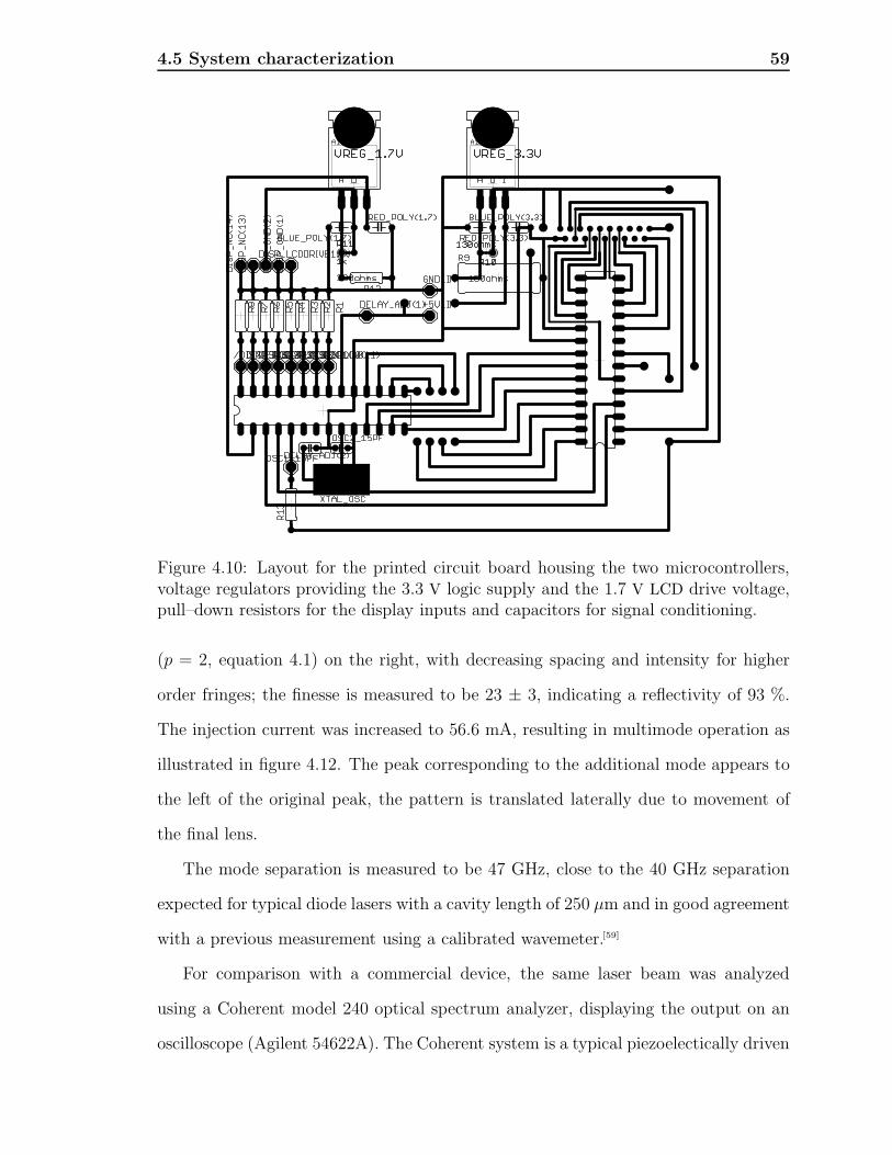
4.5 System characterization 59
Figure 4.10: Layout for the printed circuit board housing the two microcontrollers,voltage regulators providing the 3.3 V logic supply and the 1.7 V LCD drive voltage,pull–down resistors for the display inputs and capacitors for signal conditioning.
(p = 2, equation 4.1) on the right, with decreasing spacing and intensity for higher
order fringes; the finesse is measured to be 23 ± 3, indicating a reflectivity of 93 %.
The injection current was increased to 56.6 mA, resulting in multimode operation as
illustrated in figure 4.12. The peak corresponding to the additional mode appears to
the left of the original peak, the pattern is translated laterally due to movement of
the final lens.
The mode separation is measured to be 47 GHz, close to the 40 GHz separation
expected for typical diode lasers with a cavity length of 250 µm and in good agreement
with a previous measurement using a calibrated wavemeter.[59]
For comparison with a commercial device, the same laser beam was analyzed
using a Coherent model 240 optical spectrum analyzer, displaying the output on an
oscilloscope (Agilent 54622A). The Coherent system is a typical piezoelectically driven

4.5 System characterization 60
Figure 4.11: Displaying single mode oper-ation of an external cavity diode laser at aninjection current of 55.5 mA.
Figure 4.12: A small reduction in injectioncurrent leads to the appearance of a secondmode to the left.
Fabry–Perot based device which produces a temporally–varying interference pattern
detected by a photodiode. With the 3.3 µW beam no signal was visible above the
noise floor; the spectrum started to emerge from the noise at a beam power of 8 µW.
An experiment was performed to assess the linearity and sensitivity of the system.
The image sensor recorded the far–field diffraction pattern from a 300 µm aperture il-
luminated by the ECDL. Nine traces were taken with the power adjusted using a linear
polarizer and the laser beam power measured directly using a Coherent LaserMate–Q
power meter. Each trace was fitted to an Airy function, from which the integrated
intensity was compared with the measured power to calculate the peak intensity.
Plotting actual intensity against the measured height of a peak in pixels produced the
calibration curve shown in figure 4.13.

4.6 Future developments 61
0 5 10 15 20 250
50
100
150
200
250
Incident Intensity ΜWcm2
Dis
play
Hei
ght
pixe
ls
Figure 4.13: Calibration curve illustrating the sensitivity and linearity of the imagesensor.
4.6 Future developments
The discussion of program extensions in section 4.4.4 illustrates the simplicity of
software modification. There are a number of specific hardware modifications that
could be made to improve the system.
The SensorPIC could trivially be made to read the eight least significant bits from
the sensor, immediately increasing the sensitivity by a factor of four; this approach
could be useful for experiments using low power lasers such as those based on nonlinear
frequency conversion, however it has not yet been implemented as it would entail beam
powers so low as to be barely visible, making alignment extremely challenging.
To increase the sensitivity without reducing the intensity at which the sensor
saturates, the entire 10–bit values output by the sensor could be used. This would
require different components than those used here: microcontrollers with 10–bit wide
ports would be needed to efficiently transfer the intensity data, while a higher LCD

4.6 Future developments 62
resolution would be needed to display the full dynamic range of 1024.
Alignment of the optics could be made quicker and more convenient by using an
optical fibre to send the beam under test into the OSA.

Chapter 5
Power Supplies
In an experimental physics lab, numerous devices must be provided with a stable,
reliable power supply. The power supplied by a DC source is given by the product
of voltage and current P = IV ; the supplies fall into two broad categories: current
supplies provide a constant current by varying the voltage as required, while voltage
supplies provide a constant voltage by similarly varying the current.
5.1 Current supply
A high power current supply is required to power the heating element for the lithium
oven to be used in the beam experiment discussed in chapter 1.
5.1.1 Initial design
The chosen design uses the emitter–follower configuration (also known as a common–
emitter). The circuit diagram illustrating the concept is shown in figure 5.1.[60]
In order to maintain a constant current for a varying load an emitter–follower
makes use of return–line current sensing. The voltage drop across a low–value, high–
power sensing resistor, on the return line to the negative electrode of a constant
voltage supply, is compared to a variable reference voltage providing the set–point.
During the construction of the device, many changes and additions were made,

5.1 Current supply 64
LOAD
VREFRSENSE
Figure 5.1: Schematic of an emitter–follower current supply; the active device is aDarlington transistor pair mounted on a heat sink. The load is floated above thesensing resistor RSENSE, while an op–amp sets the current such that the voltage dropacross the sensing resistor remains equal to the reference voltage VREF at all times.
some for convenience, customization and safety, others to deal with fundamental prob-
lems in the design. There were three major design issues encountered:
1. Power dissipated in the sensing resistor
All main–line current must flow through the sensing resistor to provide a mea-
surement for the negative feedback loop used to set the current. At high currents
the sensing resistor will dissipate a significant amount of power (P = I2R, for
a 4 A current flowing through a 1 Ω resistor, this amounts to 16 W of power).
Two different approaches were used to deal with this.

5.1 Current supply 65
• High power resistors with good heat–sinking
• Two different values of RSENSE selectable for different current levels (1 Ω
for 0 ≤ I < 2, 0.5 Ω for 2 ≤ I ≤ 4)
As the set–point voltage VREF is compared to the voltage across RSENSE, the
different resistor values require different set–point voltage ranges to ensure the
mainline current remains within an acceptable range.
2. Power dissipated in the transistor
In terms of impedance, a transistor works much like a variable resistor with
the resistance determined by the base current. For small base currents the
collector–emitter impedance is high and the total load seen by the voltage supply
is dominated by the transistor, leading to significant power dissipation in the
transistor and ultimately to overheating.
The original design illustrated in figure 5.1 used a heat–sunk Darlington pair in
place of a single NPN transistor in order to dissipate excess heat, however these
measures proved inadequate given the power requirements of the unit. The final
design, shown in figure 5.3, took this concept further.
• Two Darlington pair transistor combinations used in parallel, cuts the
power dissipated in each by half
• An individual heat–sink for each Darlington pair, mounted externally to
promote convective heat dissipation
3. Maintaining an adequate base–emitter voltage
A Darlington pair requires a 1.2 V base–emitter voltage before any collector–
emitter current will flow. At high current levels the voltage drop across the load
is such that the op-amp providing the base current cannot provide a sufficiently
high voltage even if it can swing to the rails.

5.1 Current supply 66
This problem could have been solved simply by furnishing the op-amp with
a higher voltage supply. However, the standard lab supplies that we use (see
section 5.2) provide a maximum of ±15 V and for the sake of convenience it
seemed worthwhile pursuing a solution which did not require a supply voltage
outside this range. The 48 V supply powering the device is not used to power
the control electronics as this could lead to instability, due to fluctuations in the
power supply being amplified by identical fluctuations in the control electronics.
The final design shown in figure 5.3 illustrates the simple solution employed.
The load is floated above the transistor which means that the output of the
op-amp need never rise above 1.2 V. The front panel of the high power current
supply is illustrated in figure 5.2.
Figure 5.2: The high power, current source power supply, with a safety guard aroundthe power transistors which have cases at high voltage.
5.1.2 A low power current supply
A simple, reliable, low power current supply is used to provide the tuning current
to the RF attenuator described in chapter 3. A voltage divider is used to tune the
gate–source voltage applied across a n–channel MOSFET. The layout is illustrated in
figure 3.6, while the current linearity is demonstrated by the trace in figure 3.12.
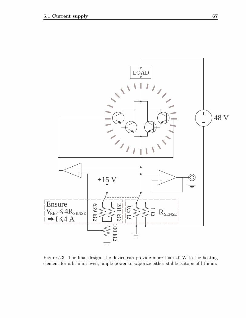
5.1 Current supply 67
LOAD
+15 V
1 Ω
0.5 Ω
639 kΩ
281 kΩ100 kΩ
48 V
REF SENSE SENSEREnsure
I 4 AV 4R
Figure 5.3: The final design; the device can provide more than 40 W to the heatingelement for a lithium oven, ample power to vaporize either stable isotope of lithium.

5.2 Voltage supply 68
5.2 Voltage supply
Figure 5.4: An image of the voltage source power supply.
A search was undertaken to ascertain the best candidate for a standard DC voltage
supply to use in the laboratory. A comparison was made of several commercial units
available and the component level alternatives.
The device purchased was a Power–One HAD–15–0.4A component level voltage
source consisting of a transformer and full–wave bridge rectifier, along with voltage
regulators and capacitors to produce a stable ±15 V source. Construction involved
mounting the device in a case with voltage regulators to provide additional outputs
at ±12 V and +5 V. Figure 5.4 shows the front panel of the finished device.

Chapter 6
The Adiabatic Theorem of
Quantum Mechanics: Beyond the
Landau–Zener Approximation
A frequently occurring problem in experimental atomic and molecular physics involves
the observation and control of a quantum mechanical system, including a perturbation
parameter, q, which changes with time. We wish to predict the final state of the system
for a given change in q.
The perturbation parameter can represent the internuclear distance during an
atomic collision, or the amplitude of an applied electric or magnetic field. After a
modification of q and a corresponding change in the system Hamiltonian, the final
state depends critically on the profile of the change in q(t) and the time τ during
which the modification takes place.[61][62]
A highly relevant example of a system undergoing such a transition is a lithium–
fluoride molecule (LiF), which can exist as a predominantly covalently bound or pre-
dominantly ionically bound molecule, Li+–F–. Figure 6.1 illustrates how these energy
states depend on the internuclear distance R; if the internuclear distance of an ion-
ically bound LiF molecule on curve X1Σ+ increases sufficiently slowly, the nature of
the bond will change such that the molecule dissociates, forming free lithium and
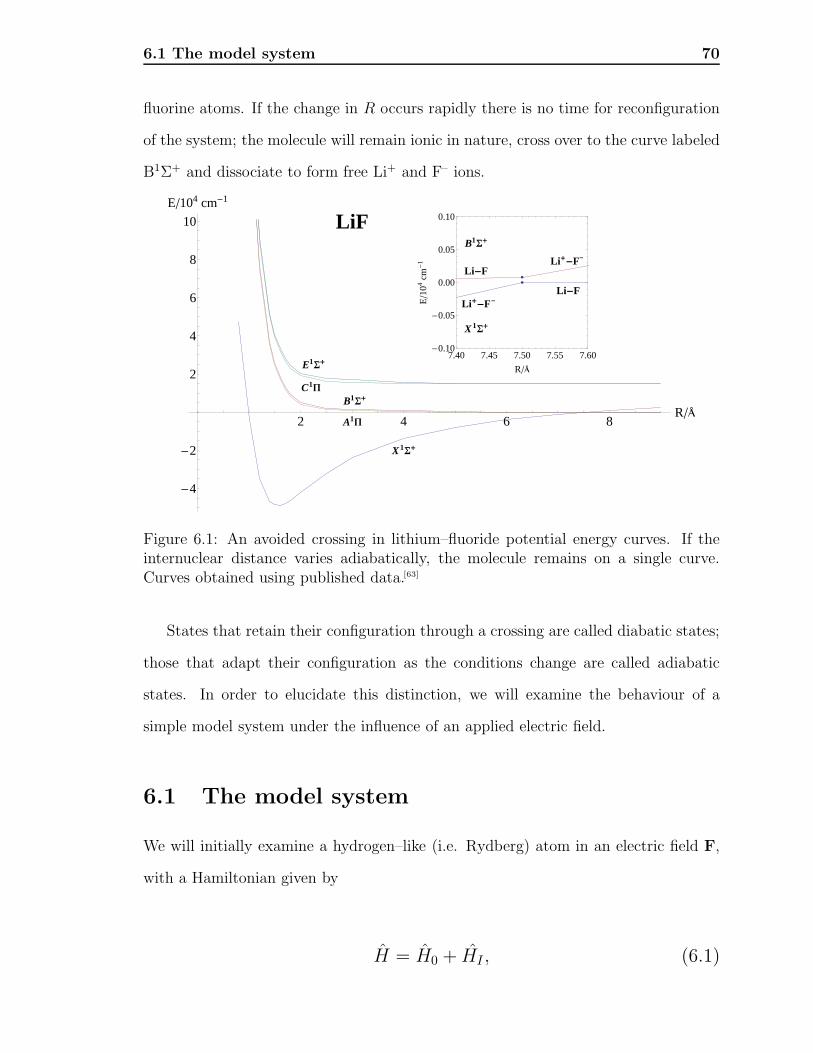
6.1 The model system 70
fluorine atoms. If the change in R occurs rapidly there is no time for reconfiguration
of the system; the molecule will remain ionic in nature, cross over to the curve labeled
B1Σ+ and dissociate to form free Li+ and F– ions.
B1
X1
E1
A1
C1
LiF
2 4 6 8R
4
2
2
4
6
8
10
E104 cm1
X1
B1
LiF
LiFLiF
LiF
7.40 7.45 7.50 7.55 7.600.10
0.05
0.00
0.05
0.10
R
E1
04cm
1
Figure 6.1: An avoided crossing in lithium–fluoride potential energy curves. If theinternuclear distance varies adiabatically, the molecule remains on a single curve.Curves obtained using published data.[63]
States that retain their configuration through a crossing are called diabatic states;
those that adapt their configuration as the conditions change are called adiabatic
states. In order to elucidate this distinction, we will examine the behaviour of a
simple model system under the influence of an applied electric field.
6.1 The model system
We will initially examine a hydrogen–like (i.e. Rydberg) atom in an electric field F,
with a Hamiltonian given by
H = H0 + HI , (6.1)

6.1 The model system 71
where H0 is the diabatic Hamiltonian, including the unperturbed kinetic and poten-
tial energy and the Stark shift due to the applied field, and HI is the interaction
Hamiltonian, which adds an additional short range 1/r2 potential due to polarization
of the core. The complete Hamiltonian for the system is given by equation 6.2,
H = − 2
2m∇2 − e2
4πε0r− d · F − A
r2 . (6.2)
6.1.1 Diabatic states
For simplicity we will include just two states in the basis |1〉, |2〉, with energies E1(F)
and E2(F), separated at F = 0 by ω0. If we take the electric field to be oriented in
the positive z–direction, we have a Hamiltonian matrix in the diabatic basis given by,
H(F ) =
⎛⎜⎝ ea0F (t) − 1
2ω0 a
a∗ 12ω0 − ea0F (t)
⎞⎟⎠ , (6.3)
where we have taken the zero point of energy to lie at the halfway point between the
two states and assumed that the magnitude of the Stark shift matrix element is the
same for the two states. It is clear that at a particular value of the applied field, the
two states are degenerate and we have a crossing.
We wish to solve the amplitude equations for the system in the Schrodinger picture,
in which the state vectors exhibit spatial dependence but no time dependence (i.e.
the phase is arbitrary, but not varying with time),
|ψ〉 = c1(t)|1〉 + c2(t)|2〉. (6.4)
The time dependence of the state vector amplitudes is given by the time–dependent
Schrodinger equation.

6.1 The model system 72
c =1
iHc. (6.5)
Note that states |1〉 and |2〉 are not eigenvectors of the Hamiltonian.
Examining equation 6.3 we can deduce the behaviour of the system under a
changing field. For a system in state |2〉, the expectation value of the energy is
given by E2(t) = ω0/2 − ea0F (t), thus the energy decreases linearly with electric
field. The expectation value of the energy for a system in state |1〉 is given by
E1(t) = ea0F (t) − ω0/2, and thus increases linearly with electric field. At time
t×, the two energies are equal, with an electric field strength given by equation 6.6.
F (t×) =ω
2ea0. (6.6)
6.1.2 Adiabatic states
We now choose to describe the system in a new basis, using as our state vectors the
eigenvectors of the Hamiltonian operator, which we denote |φ1(t)〉 and |φ2(t)〉 with
energies given by the eigenvalues ε1(t) and ε2(t). The system wavefunction given
in the diabatic basis by equation 6.4, can also be given in the adiabatic basis as in
equation 6.7,
|ψ〉 = cA1 (t)|φ1(t)〉 + cA2 (t)|φ2(t)〉. (6.7)
The inclusion of the perturbative interaction Hamiltonian couples the levels, break-
ing the degeneracy and ensuring that the eigenvalues of the Hamiltonian remain dis-
tinct,

6.1 The model system 73
ε1(t) = ε2(t), ∀ t.
At time t× (see equation 6.6) the adiabatic energies have the lowest energy separa-
tion ε2(t×)− ε1(t×) = 2|a|. Note that a does not vary with time. In the general case,
the coupling is a function of the perturbation variable and, therefore, does depend on
time. The energy eigenvalues, ε1(F ) and ε2(F ), are hyperbolae that each approach
E1(F ) and E2(F ) asymptotically.
0 0.2 0.4 0.6 0.8 1
−0.6
−0.4
−0.2
0
0.2
0.4
0.6
Electric field
Ene
rgy
ε1(F) ε
2(F) E
1(F) E
2(F)
Figure 6.2: Level energies of the diabatic (E1(F ), E2(F )) and adiabatic (ε1(F ), ε2(F ))states. Finite coupling between the states leads to the avoided crossing for a systemfollowing an adiabatic path.
For a time–independent system, the energy eigenvalues are obtained by diagonal-
izing the Hamiltonian with a time–independent unitary transformation. If the system
evolves sufficiently slowly (adiabatic evolution) then the energy eigenvalues calculated
for the time–independent solution remain valid. The unitary transformation matrix

6.1 The model system 74
is constructed from the eigenvectors |φ1〉, |φ2〉.
|φ1〉 =
⎛⎜⎝ φ
(1)1
φ(2)1
⎞⎟⎠ |φ2〉 =
⎛⎜⎝ φ
(1)2
φ(2)2
⎞⎟⎠ , (6.8)
giving a transformation matrix U,
U=
⎛⎜⎝ φ
(1)1 φ
(1)2
φ(2)1 φ
(2)2
⎞⎟⎠ , (6.9)
which can be used to obtain the diagonalized Hamiltonian HD through the unitary
transformation,
HD = U−1HU=
⎛⎜⎝ −ε 0
0 +ε
⎞⎟⎠ , (6.10)
where the diagonal elements are the eigenvalues of the Hamiltonian matrix in equation
6.3, given by
±ε = ±√(
ea0F (t) − 1
2ω0
)2
+ a2. (6.11)
For a system which changes with time the adiabatic eigenvectors can be obtained
from the diabatic state vectors, using the same transformation matrix,
⎛⎜⎝ |φ1(t)〉
|φ2(t)〉
⎞⎟⎠ = U−1(t)
⎛⎜⎝ |1〉
|2〉
⎞⎟⎠ . (6.12)
The full time–dependence of the state vector in the adiabatic basis can be obtained
from the transformed Hamiltonian given in equation 6.13.[64] The full derivation is

6.2 The adiabatic theorem 75
given in appendix B.
HA = U−1HU− iU−1 d
dtU, (6.13)
giving the full, time–dependent, adiabatic Hamiltonian:
Had =
⎛⎜⎝ −ε −iγ
iγ ε
⎞⎟⎠ , (6.14)
where
γ =aea0
2ε
dF
dt,
giving equations of motion for the adiabatic states:
dcA1dt
=iε(t)
cA1 (t) − γ(t)
cA2 (t), (6.15)
dcA2dt
=γ(t)
cA1 (t) − iε(t)
cA2 (t). (6.16)
6.2 The adiabatic theorem
If we define the time–evolution operator T (t, t0) by the integral equation
T (t, t0) = 1 − i
∫ t
t0
H(t′)T (t′, t0)dt′ (6.17)
then it can be used to determine the dynamic evolution of the system through equation
6.18.

6.2 The adiabatic theorem 76
ψ(t) = T (t, t0)ψ(t0) (6.18)
where the duration of the evolution is given by τ = t− t0.
The problem described at the beginning of this chapter is now simply to determine
how T (t, t0) depends on τ . In the limit τ → 0 for a given final state, we have an
infinitely rapid passage and the dynamical state of the system remains unchanged,
limτ→0
T (t, t0) = 1, (6.19)
the system follows the diabatic path.
In the limit τ → ∞, for a given final state we have an infinitely slow passage. If
the system is initially in an eigenstate of H(t0), it will pass through the corresponding
stationary states of H(t) for all t, ending in a stationary state of H(t). This important
result is known as the adiabatic theorem of quantum mechanics.[65]
6.2.1 The Landau–Zener Approximation
For a fully quantum–mechanical treatment of a general system, the equations of mo-
tion for the system (equations 6.5) cannot be solved analytically. In 1932, two closely
related papers by Landau[66] and Zener[67] were published on the subject of diabatic
transitions between quantum states. Such transitions occur between states of the en-
tire system, hence any description of the system must include all external influences,
including collisions and external electric and magnetic fields.
In order that the equations of motion for the system might be solved analytically,
a set of simplifications are made, known collectively as the Landau–Zener approxima-
tion. The simplifications are as follows:
1. The perturbation parameter is a known, linear function of time

6.2 The adiabatic theorem 77
2. The energy separation of the diabatic states varies linearly with time
3. The coupling a in the diabatic Hamiltonian matrix is independent of time
The first simplification makes this a semi-classical treatment. In the case of our
model system, a Rydberg atom in an electric field, the field strength becomes a classi-
cal variable which can be precisely measured during the transition. This requirement
is quite restrictive as a linear change may not be the optimal profile to achieve the
desired transition probability.
The second simplification allows us to make the substitution E2(t) − E1(t) ≡ αt;
for our model system this corresponds to a linear change in electric field strength. For
a linear Stark shift this follows directly from point 1.
The final simplification requires that the time–dependent perturbation does not
couple the diabatic states; rather, the coupling must be due to a static deviation from
a 1/r coulomb potential, commonly described by a quantum defect.
The details of Zener’s solution are somewhat opaque, relying on a set of substitu-
tions to put the equation of motion into the form of the Weber equation1 and using
the known solution. A more transparent solution is provided by Wittig using contour
integration.[68]
Probability calculations
A key figure of merit is known as the Landau–Zener velocity vLZ , given in general by
vLZ =
∂
∂t|E2 − E1|
∂
∂q|E2 − E1|
≈ dq
dt. (6.20)
Zener’s model system used the internuclear distance within a diatomic molecule
as the perturbation variable with the consequence that his vLZ was in fact the relative
1See Handbook of Mathematical Functions, 9th edition, M. Abramowitz and I. A. Stegun, p. 498.
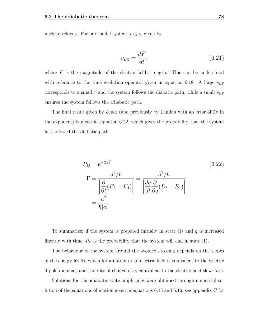
6.2 The adiabatic theorem 78
nuclear velocity. For our model system, vLZ is given by
vLZ =dF
dt, (6.21)
where F is the magnitude of the electric field strength. This can be understood
with reference to the time evolution operator given in equation 6.18. A large vLZ
corresponds to a small τ and the system follows the diabatic path, while a small vLZ
ensures the system follows the adiabatic path.
The final result given by Zener (and previously by Landau with an error of 2π in
the exponent) is given in equation 6.22, which gives the probability that the system
has followed the diabatic path.
PD = e−2πΓ (6.22)
Γ =a2/∣∣∣∣ ∂∂t(E2 − E1)
∣∣∣∣=
a2/∣∣∣∣dqdt ∂∂q(E2 − E1)
∣∣∣∣=
a2
|α|
To summarize; if the system is prepared initially in state |1〉 and q is increased
linearly with time, PD is the probability that the system will end in state |1〉.The behaviour of the system around the avoided crossing depends on the slopes
of the energy levels, which for an atom in an electric field is equivalent to the electric
dipole moment, and the rate of change of q, equivalent to the electric field slew–rate.
Solutions for the adiabatic state amplitudes were obtained through numerical so-
lution of the equations of motion given in equations 6.15 and 6.16; see appendix C for

6.2 The adiabatic theorem 79
code implementing these solutions. As a test of these solutions, the probability of a
diabatic transition was compared with that predicted by the Landau–Zener formula,
under the required conditions, for a variety of field slew–rates. The results are shown
in figure 6.3.
0 5 10 15 20 25 300
0.1
0.2
0.3
0.4
0.5
0.6
0.7
0.8
0.9
Field gradient (arb. units)
Dia
batic
tran
sitio
n pr
obab
ility Numerical calculation
Landau−Zener
Figure 6.3: Comparing the results of a numerical solution with the Landau–Zener so-lution; the curve representing the Landau–Zener solutions has been translated slightlyfor clarity.
6.2.2 Beyond the Landau–Zener approximation
Having established the veracity of the numerical solutions, we now have the tools to
move beyond the restrictions imposed by the Landau–Zener formula. We are able to
observe the probability of a diabatic transition, for any arbitrary electric field profile.
Figure 6.4 shows the effects of three different field profiles on the adiabatic state
energies and populations. While the three profiles are different, the durations of the

6.2 The adiabatic theorem 80
−4 −2 0 2 4
−50
0
50F
ield
str
engt
h(a)
−4 −2 0 2 4
−50
0
50
Ene
rgy
−4 −2 0 2 40
0.5
1
Pdiabatic
= 0.81
Time
Pop
ulat
ions
−4 −2 0 2 4
−50
0
50
(b)
−4 −2 0 2 4
−50
0
50
−4 −2 0 2 40
0.5
1
Pdiabatic
= 0.88
Time
−4 −2 0 2 4
−50
0
50
(c)
−4 −2 0 2 4
−50
0
50
−4 −2 0 2 40
0.5
1
Pdiabatic
= 0.35
Time
Figure 6.4: Adiabatic state populations and energies for different field ramp profiles.Note that the linear ramp leads to the highest probability of a diabatic transition.
interactions and the total field strength changes are identical.
It is immediately clear that restricting oneself to profiles that can be described
by the Landau–Zener formula is extremely problematic if the probability of a dia-
batic transition is to be minimized. By reducing the Landau–Zener velocity (time–
derivative of the electric field strength) at the time when the two states are ener-
getically closest, the probability of a diabatic transition can be significantly reduced
compared to the Landau–Zener case.
Obtaining the profile that minimizes the diabatic transition probability for a given

6.2 The adiabatic theorem 81
duration and change in field strength will be left for future work.

Chapter 7
Adiabatic Population Transfer
The ability to precisely control the state of a population of atoms or molecules is the
key to the efficient production of electronic Rydberg states and opens up pathways
through the energy level manifolds to heavy Rydberg states just below the continuum.
Optical excitation using a narrow–band laser light source can be used effectively
to populate an excited state separated from the ground state by the laser frequency.
However, the state remains coupled to the light field, and stimulated emission can
lead to rapid depletion of the excited state population.
For a certain class of atomic and molecular systems, there exists a coherent su-
perposition of low lying states which does not couple to the light field. Consequently
the population is effectively trapped, in a phenomenon known as coherent population
trapping (CPT).[69] The use of the non–coupled or “dark” state as a bridging state to
effect transfer between the two constituent states provides a powerful tool for precise
control over the energetic states of atoms and molecules.
The code used to implement solutions to the amplitude equations describing the
population dynamics of multi–level systems is given in appendix D.

7.1 The 3–level system: Λ configuration 83
7.1 The 3–level system: Λ configuration
The simplest system in which coherent population trapping can be observed is a
3–level system in the Λ configuration; see figure 7.1. Such systems appear in the
energy level schemes of most, if not all, atomic and molecular species. In a real
physical system the dynamics are complicated by the presence of additional states in
the energetic vicinity of the target Λ system; a model system, comprising only the
requisite three levels, serves to simplify the problem.
7.1.1 Features of the Λ system
• Closely spaced “ground” states |1〉 and |2〉
• Large separation between ground states and excited state |3〉• The |1〉 ↔ |2〉 transition is dipole forbidden
• Monochromatic light fields, with frequencies ωL13 and ωL
23, near–resonant with
|1〉 ↔ |3〉 and |2〉 ↔ |3〉 transitions respectively, henceforth referred to as laser
1 and laser 2
• ∆1 and ∆2 are detunings for each transition, ∆x = wLx3 − ω3x
• Ω31 and Ω32 are the Rabi frequencies for the transitions and the respective laser
beams, Ωij =e〈i|r|j〉. E0
• Separation of ground states sufficient to prevent ‘crosstalk’, i.e. Ω3x depends
only on intensity of light with frequency ωx
• Relaxation from |3〉 with rate Γ, to states outside the Λ–system. No relaxation
within system
Note: figure captions include a statement of conditions in the form:
[ρ011,ρ
022,ρ
033],[∆1 (s−1),∆2 (s−1)],
[Ω31
ea0(1000 Vm−1)/, Ω32
ea0(1000 Vm−1)/
],Γ (s−1)],
where ρ0ii is the initial population of state |i〉 and the Rabi frequency is given in units
of ea0(1000 Vm−1)/ = 8.08×10⁷ s−1. For reference, a laser intensity of 1 mWmm−2,

7.1 The 3–level system: Λ configuration 84
with a transition dipole moment of ea0, gives Ω = 7.01×10⁷s−1. The Rabi frequencies
noted for the adiabatic population transfer figures are peak values.
ΩΩ
31
32ω23
∆1 ∆23
ΓL
12
ω13L
Figure 7.1: Energy level scheme of a 3–level system in a Λ configuration, including theRabi frequency for each allowed transition and corresponding light field, the frequencyof each light field, the detunings and the excited state decay rate.
The system wavefunction in the interaction picture is given by
|Ψ〉 =3∑
n=1
cne−iEnt/|n〉. (7.1)
Through a judicious choice of phase factors, explicit time dependence can be removed
from the Hamiltonian matrix:
c1 = c1
c2 = c2ei(∆1−∆2)t/ (7.2)
c3 = c3ei∆1t/

7.1 The 3–level system: Λ configuration 85
From the time–dependent Schrodinger equation,
id
dtc = Hc, (7.3)
we derive the equations of motion for the state amplitudes within the Λ system:
⎛⎜⎜⎜⎜⎜⎜⎜⎜⎜⎝
c1
c2
c3
⎞⎟⎟⎟⎟⎟⎟⎟⎟⎟⎠
=
⎛⎜⎜⎜⎜⎜⎜⎜⎜⎜⎝
0 0 −iΩ∗312
0 i(∆1 − ∆2) −iΩ∗322
−iΩ312 −iΩ32
2 i∆1 − Γ2
⎞⎟⎟⎟⎟⎟⎟⎟⎟⎟⎠
⎛⎜⎜⎜⎜⎜⎜⎜⎜⎜⎝
c1
c2
c3
⎞⎟⎟⎟⎟⎟⎟⎟⎟⎟⎠. (7.4)
7.1.2 Coherent Population Trapping
Figure 7.2 shows the population dynamic of a 3–level system iluminated with two light
fields, resonant with the two dipole allowed transitions, with no relaxation. Figure
7.3 shows the same system with relaxation from the excited state, illustrating the
concept of coherent population trapping in which there is a coherent superposition of
ground states |1〉 and |2〉 which will not absorb energy from either light field and is
hence not coupled to state |3〉. As atoms in this state are non–absorbing, this effect
is also known as electromagnetically induced transparency.
To further understand this phenomenon it is instructive to examine the system in
a new basis. The ground states are now represented by the non–absorbing dark state,

7.1 The 3–level system: Λ configuration 86
0 0.05 0.1 0.15 0.20
0.2
0.4
0.6
0.8
1
Time [µs]
ρ11
ρ22
ρ33
Figure 7.2: Rabi flopping in a 3–level Λ sys-tem; population oscillates between states |1〉and |2〉, passing through state |3〉, with nomore than half the population in the excitedstate at any time. [1,0,0],[0,0],[1,1],0
0 0.5 1 1.5 20
0.2
0.4
0.6
0.8
1
Time [µs]
ρ11
ρ22
ρ33
Figure 7.3: Coherent population trappingin a 3–level Λ system; relaxation from state|3〉 decreases the total system population,however a finite steady state population re-mains, split between states |1〉 and |2〉.
|D〉, and an absorbing state, |A〉; the excited state |3〉 remains.
|D〉 =
(Ω32
Ω
)|1〉 −
(Ω31
Ω
)|2〉 (7.5)
|A〉 =
(Ω∗
31
Ω
)|1〉 +
(Ω∗
32
Ω
)|2〉 (7.6)
|3〉 = |3〉
Ω =√
|Ω31|2 + |Ω32|2
On deriving the Hamiltonian matrix in the new basis, the condition under which
the dark state is decoupled from the light fields is immediately clear. Under the
condition known as Raman detuning, expressed mathematically as ∆1 = ∆2, the rate

7.1 The 3–level system: Λ configuration 87
of change of the dark state amplitude is identically zero.
⎛⎜⎜⎜⎜⎜⎜⎜⎜⎜⎝
˙cD
˙cA
c3
⎞⎟⎟⎟⎟⎟⎟⎟⎟⎟⎠
=
⎛⎜⎜⎜⎜⎜⎜⎜⎜⎜⎝
i(∆1 − ∆2)|Ω31|2
Ω2 −i(∆1 − ∆2)Ω∗
31Ω∗32
Ω2 0
−i(∆1 − ∆2)Ω31Ω32
Ω2 i(∆1 − ∆2)|Ω32|2
Ω2 −iΩ2
0 −iΩ2 i∆1 − Γ2
⎞⎟⎟⎟⎟⎟⎟⎟⎟⎟⎠
⎛⎜⎜⎜⎜⎜⎜⎜⎜⎜⎝
cD
cA
c3
⎞⎟⎟⎟⎟⎟⎟⎟⎟⎟⎠
. (7.7)
Figure 7.4 illustrates the behaviour of the same system, under the same conditions,
as figure 7.3, described in the dark/absorbing basis. The steady state population is
entirely in the dark state, which has remained unaffected by relaxation from the
excited state. The oscillation and decay of the population in states |1〉 and |2〉 are
entirely in the absorbing state.
0 0.5 1 1.5 20
0.1
0.2
0.3
0.4
0.5
Time [µs]
ρDD
ρAA
ρ33
Figure 7.4: Coherent population trapping in a 3–level Λ system, examined in thedark/absorbing basis. The population of the dark state remains constant, resulting inthe observed steady state population; the decay from states |1〉 and |2〉 is due to thecoupling between the absorbing state, and the excited state with its finite relaxationrate. [1,0,0],[0,0],[1,1],107
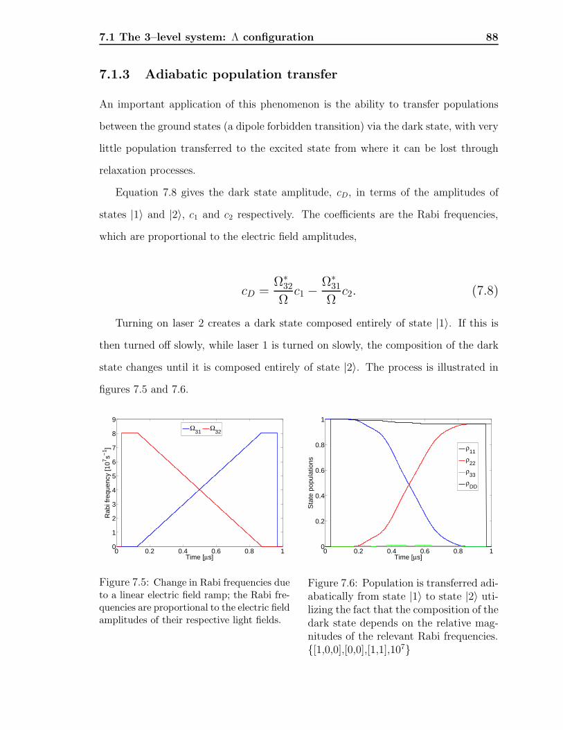
7.1 The 3–level system: Λ configuration 88
7.1.3 Adiabatic population transfer
An important application of this phenomenon is the ability to transfer populations
between the ground states (a dipole forbidden transition) via the dark state, with very
little population transferred to the excited state from where it can be lost through
relaxation processes.
Equation 7.8 gives the dark state amplitude, cD, in terms of the amplitudes of
states |1〉 and |2〉, c1 and c2 respectively. The coefficients are the Rabi frequencies,
which are proportional to the electric field amplitudes,
cD =Ω∗
32
Ωc1 − Ω∗
31
Ωc2. (7.8)
Turning on laser 2 creates a dark state composed entirely of state |1〉. If this is
then turned off slowly, while laser 1 is turned on slowly, the composition of the dark
state changes until it is composed entirely of state |2〉. The process is illustrated in
figures 7.5 and 7.6.
0 0.2 0.4 0.6 0.8 10
1
2
3
4
5
6
7
8
9
Time [µs]
Rab
i fre
quen
cy [1
07 s−1 ]
Ω31
Ω32
Figure 7.5: Change in Rabi frequencies dueto a linear electric field ramp; the Rabi fre-quencies are proportional to the electric fieldamplitudes of their respective light fields.
0 0.2 0.4 0.6 0.8 10
0.2
0.4
0.6
0.8
1
Time [µs]
Sta
te p
opul
atio
ns
ρ11
ρ22
ρ33
ρDD
Figure 7.6: Population is transferred adi-abatically from state |1〉 to state |2〉 uti-lizing the fact that the composition of thedark state depends on the relative mag-nitudes of the relevant Rabi frequencies.[1,0,0],[0,0],[1,1],107

7.1 The 3–level system: Λ configuration 89
0 5 10 15 20 250
0.2
0.4
0.6
0.8
1
Electric field slew rate [Vm−1/ns]
Pop
ulat
ion
loss
Figure 7.7: Population loss as a function of electric field slew rate; note the nearlylinear relationship at rates below about 4 Vm-1/ns. [1,0,0],[0,0],[1,1],107
Note that a truly adiabatic process occurs at a rate of zero; the non-zero rate of
the electric field ramps leads to a finite non–adiabaticity, resulting in some population
transfer to state |3〉, and hence the population loss through relaxation seen in figure
7.6, given by
population loss = Γ
∫ρ33 dt. (7.9)
In order to quantify this, a series of simulations were done using different rates;
the results are shown in figure 7.7.
The population transfer shown in figure 7.6 is accomplished using a linear change
in electric field strength. In order to simulate more realistic experimental conditions,
two other forms were investigated.
There are numerous ways to directly control laser intensity. These can be as simple
as adjusting the injection current supplied to a diode laser, however the changing

7.1 The 3–level system: Λ configuration 90
charge density in the cavity will modify the frequency emitted by the laser. A practical
solution is to pass a laser, resonant with the |1〉 ↔ |3〉 transition, through an acousto–
optic modulator (see section 3.1.3) such that the diffracted beam is downshifted by
the ground state splitting. The amplitudes of the diffracted and undiffracted beams
depend on the amplitude of the acoustic wave, which can be controlled by varying
the applied RF bias. Intensity is related to electric field amplitude by
I =1
2cε0| E0|2. (7.10)
Figure 7.9 shows the results of a simulated population transfer achieved with a
linear change in intensity; figure 7.8 illustrates the changes in the Rabi frequencies
during this process. This was expected to give a very similar result to that achieved
with a linear change in electric field strength, possibly with a slightly larger population
loss due to the rapid initial change in electric field strength. In fact the results show
dramatic oscillations, which are difficult to relate to changing Rabi frequencies. As
yet the oscillations are unexplained and may be an artifact of the simulation.
0 0.2 0.4 0.6 0.8 10
1
2
3
4
5
6
7
8
9
Time [µs]
Rab
i fre
quen
cy [1
07 s−1 ]
Ω31
Ω32
Figure 7.8: Change in Rabi frequencies dueto a linear change in intensity.
0 0.2 0.4 0.6 0.8 10
0.2
0.4
0.6
0.8
1
Time [µs]
Sta
te p
opul
atio
ns
ρ11
ρ22
ρ33
ρDD
Figure 7.9: Population transfer still oc-curs, however there is an unexplained os-cillation which may or may not be physical.[1,0,0],[0,0],[1,1],107
There is a technique for implementing adiabatic population transfer in an atomic or

7.1 The 3–level system: Λ configuration 91
molecular beam, known as stimulated Raman adiabatic passage (STIRAP).[70] Atoms
or molecules passing consecutively through the overlapped beams of lasers 2 and 1
experience a pair of approximately Gaussian intensity profiles due to the two beams.
If the two beams are parallel and partially overlap it should effect adiabatic population
transfer; i.e. a dark state composed entirely of state |1〉 is created as an atom enters
the beam of laser 2; as it passes into the beam of laser 1, the composition of the dark
state will change until it is entirely composed of state |2〉. Once out of the beam
region there will be no dark state and the atom will simply be in state |2〉.A simulation of the beam experiment was constructed including the likely experi-
mental conditions. The beamwidth was chosen to be 1 mm; the velocity of the atoms
was calculated using equation 7.11 and assuming 7Li was vaporised at an oven temper-
ature of 500C, leading to a velocity of approximately 1500 ms−1. Figure 7.10 shows
how the Rabi frequencies vary as the atoms traverse the beam; figure 7.11 shows the
resulting changes in the populations of the states.
v =
√3kT
m(7.11)
7.1.4 Departure from Raman detuning
The existence of the dark state depends on a condition known as Raman detuning,
whereby the detunings of the lasers from their respective transitions are equal; ∆12 =
∆1 − ∆2 = 0 (see figure 7.1). In an experimental setting such requirements can
never be met exactly and it becomes useful to know how sensitive the system is to
deviations from ideal conditions. With perfect Raman detuning, we expect a steady
state population of 0.5 (see figure 7.3). Any deviation from this will lead to population
decay, eventually resulting in total depopulation of the system. By approximating the
decay as exponential, a time constant can be calculated giving a quantitative measure
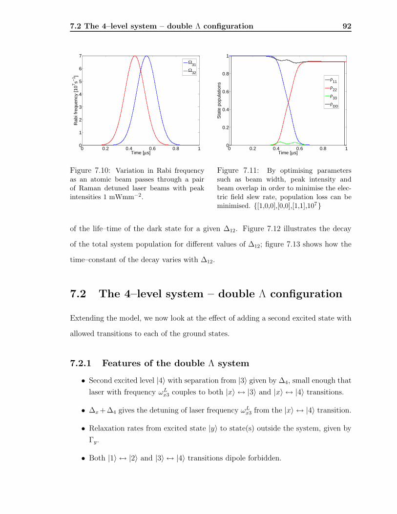
7.2 The 4–level system – double Λ configuration 92
0 0.2 0.4 0.6 0.8 10
1
2
3
4
5
6
7
Time [µs]
Rab
i fre
quen
cy [1
07 s−1 ]
Ω31
Ω32
Figure 7.10: Variation in Rabi frequencyas an atomic beam passes through a pairof Raman detuned laser beams with peakintensities 1 mWmm−2.
0 0.2 0.4 0.6 0.8 10
0.2
0.4
0.6
0.8
1
Time [µs]
Sta
te p
opul
atio
ns
ρ11
ρ22
ρ33
ρDD
Figure 7.11: By optimising parameterssuch as beam width, peak intensity andbeam overlap in order to minimise the elec-tric field slew rate, population loss can beminimised. [1,0,0],[0,0],[1,1],107
of the life–time of the dark state for a given ∆12. Figure 7.12 illustrates the decay
of the total system population for different values of ∆12; figure 7.13 shows how the
time–constant of the decay varies with ∆12.
7.2 The 4–level system – double Λ configuration
Extending the model, we now look at the effect of adding a second excited state with
allowed transitions to each of the ground states.
7.2.1 Features of the double Λ system
• Second excited level |4〉 with separation from |3〉 given by ∆4, small enough that
laser with frequency ωLx3 couples to both |x〉 ↔ |3〉 and |x〉 ↔ |4〉 transitions.
• ∆x +∆4 gives the detuning of laser frequency ωLx3 from the |x〉 ↔ |4〉 transition.
• Relaxation rates from excited state |y〉 to state(s) outside the system, given by
Γy.
• Both |1〉 ↔ |2〉 and |3〉 ↔ |4〉 transitions dipole forbidden.

7.2 The 4–level system – double Λ configuration 93
0 0.1 0.2 0.3 0.4 0.50.4
0.5
0.6
0.7
0.8
0.9
1
Time [µs]
Sys
tem
pop
ulat
ion
|∆12
| = 0
|∆12
| = 1 MHz
|∆12
| = 2 MHz
|∆12
| = 3 MHz
|∆12
| = 4 MHz
Figure 7.12: As ωL13 increases, ∆12 = ∆1 −
∆2 increases leading to a more rapid decay.[1,0,0],[0,0],[1,1],107
0 2 4 6 8 10 120.2
0.4
0.6
0.8
1
|∆12
| [MHz]
Tim
e−co
nsta
nt [µ
s]
Figure 7.13: As the system moves fur-ther from Raman detuning the decay time–constant decreases. At a certain point ∆1
is such that the slow transfer of populationfrom |1〉 to |3〉 increases the time–constant.
• Again no relaxation within the system.
The double Λ system illustrated in figure 7.14 displays much of the same behaviour
as the Λ system illustrated in figure 7.1, the lasers tuned to the |x〉 ↔ |3〉 transitions
couple only weakly to the |x〉 ↔ |4〉 transitions. There is however a stringent addi-
tional condition required to produce a dark state which is associated with any system
that allows different paths to be taken between the ground states. Known as closed
level schemes, the existence of a dark state in such systems shows a strong dependence
on the phase of the wavefunction, including the phase of the atom and the phases of
the light fields.[71] A nice analogy is a wave on a piece of string; the wave can have
any phase until the string is closed to form a loop, at which point the phase difference
around the loop must be an integer multiple of 2π. The phase condition is given by
equation 7.12,
Φ = Φatom + (φ13 − φ23) = 2πn, n = 1, 2, 3, ..., (7.12)
Φatom = (χ1 − χ2) − (χ3 − χ4),

7.2 The 4–level system – double Λ configuration 94
Ω
∆1 ∆2 ∆4
12
43
Γ3
Γ4ω13
L
ω13L
ω23L
ω23L
31
Ω32
Ω42
Ω41
Figure 7.14: Energy level scheme of a 4–level system in a double Λ configuration,including the Rabi frequency for each allowed transition and corresponding light field,the frequency of each light field, the detunings and the excited state decay rate. Anexample of such a system is the hyperfine structure of the D1 line in lithium–6 andlithium–7, see figure 3.1.
where φx3 is the initial phase of the laser with frequency ωLx3 and χy is the initial
phase of the 〈y|d|y〉 element of the electric dipole matrix.
Both stable isotopes of lithium (6Li and 7Li) have a classic double Λ system in the
hyperfine structure of the 2S1/2 ↔ 2P1/2 transition, see figure 3.1.
Note: Subsequent figure captions include a statement of conditions in the form:
[ρ011,ρ
022,ρ
033,ρ
044],[∆1 (s−1),∆2 (s−1)], 1
ea0(1000 Vm−1)/[Ω31,Ω32,Ω41,Ω42],[Γ3 (s−1),Γ4 (s−1)].
Figures 7.15 and 7.16 show the level populations in the 4 level system with relax-
ation from states |3〉 and |4〉. Figure 7.15 shows the evolution of the system under the
symmetric phase condition described in equation 7.12, equivalent to the statements:
|Ω41||Ω31| =
|Ω42||Ω32| , Ωij = |Ωij|eiθij (7.13)
Θ = (θ42 − θ32) − (θ41 − θ31) = 2nπ, n = 1, 2, 3, ...

7.2 The 4–level system – double Λ configuration 95
Figure 7.16 shows the result of deviation from symmetric phase: the dark state
decays even though the Raman detuning condition is satisfied.
0 0.5 1 1.5 20
0.2
0.4
0.6
0.8
1
Time [µs]
4−level system, symmetric phase
ρ11
ρ22
ρ33
ρ44
Figure 7.15: Coherent populationtrapping in a double Λ system un-der a symmetric phase condition.[1,0,0,0],[0,0],[1,1,1,1],[107 ,108]
0 0.5 1 1.5 20
0.2
0.4
0.6
0.8
1
Time [µs]
4−level system, antisymmetric phase
ρ11
ρ22
ρ33
ρ44
Figure 7.16: Under a non–symmetric phasecondition, the dark state population decays.[1,0,0,0],[0,0],[1,1,1,-1],[107 ,108]
7.2.2 Decoupling the 4th level
The frequency splitting ∆4 between the two excited levels is important in determining
the strength of the phase dependence. As ∆4 → ∞, state |4〉 is decoupled from the
system and we have a 3–level Λ system with no phase dependence. In order to quantify
this effect, a study was made of the dark state lifetime as a function of ∆4. In the
anti–symmetric phase condition described by equation 7.14, there is no dark state; the
system absorbs energy from the light fields and decays rapidly due to the relaxation
from states |3〉 and |4〉.
Φ = Φatom + (φ13 − φ23) = (2n+ 1)π, n = 1, 2, 3, ... (7.14)
Figures 7.17 and 7.18 demonstrate how increasing the frequency splitting between
|3〉 and |4〉 increases the time constant of this decay, by decoupling the 4th level.
These results demonstrate the potential of phase–dependent coherent population

7.2 The 4–level system – double Λ configuration 96
0 0.1 0.2 0.3 0.4 0.50.2
0.4
0.6
0.8
1
1.2
Time [µs]
Sys
tem
pop
ulat
ion
Population decay
+0+20 MHz+40 MHz+60 MHz+80 MHz
Figure 7.17: Decoupling the 4th level. De-cay of the total system population is slowerfor a larger ∆4 due to the weaker cou-pling between the light fields and state |4〉(smaller Ω41 and Ω42, due to less overlap be-tween state |4〉 and the ground states, hencesmaller 〈4|r|x〉). [1,0,0,0],[0,0],[1,1,1,-1],[107,108]
80 100 120 140 160 180 2000.45
0.5
0.55
0.6
0.65
0.7Time constant of the decay
∆4 [MHz]
Tim
e−co
nsta
nt [µ
s]
Figure 7.18: Modelling the decay as expo-nential, the time constants are calculated fora range of values of ∆4.
trapping as the basis for future experiments involving coherent control of quantum
systems. Using the AOM driver presented in chapter 3, direct control of the phase of
the light field is simply a matter of providing a tuning voltage to the RF phase shifter,
providing a simple mechanism for control over the existence of the dark state.

Chapter 8
Conclusions and Future Work
Significant progress has been made in the provision of tools to facilitate efficient
production of heavy Rydberg systems.
The construction of a full–featured, low–cost driver for an acousto–optic modulator
began a series of projects aimed at providing a recently established experimental
physics laboratory with the tools required for experiments planned for the near future.
Characterization of this device has demonstrated its utility for the purpose of accessing
hyperfine transitions within the D1 and D2 lines of the stable isotopes of lithium.
Many of the planned experiments will require lasers to operate on a single longi-
tudinal mode. A device has been realized which enables real time monitoring of the
mode structure of CW lasers, using as little as 3.3 µW from the beam under analysis.
Should it become necessary to decrease this power requirement, a fourfold increase
in sensitivity could be trivially introduced by reading the eight least significant bits
from the sensor. In addition, future work may include adaptation for use with pulsed
lasers, as described in Program extensions, section 4.4.4. Through the construction
of this device, the applicability of programmable microcontrollers to the solution of
problems encountered in experimental physics has been clearly demonstrated.
Results from numerical calculations showing the behaviour of a model quantum
system in the vicinity of an avoided crossing have been presented, shedding light on
a mechanism behind the formation of heavy Rydberg states from covalently bound

98
molecules. The fundamental importance of the adiabatic theorem and the calculation
of diabatic transition probabilities give this model system a wide applicability across
a range of topics in atomic and molecular physics. These include collision theory,
the design and implementation of magnetic and magneto–optical traps, and spectro-
scopic studies based on field ionization and dissociation. Limitations inherent in the
assumptions made while deriving the Landau–Zener formula have been demonstrated,
and numerical results for conditions violating these assumptions have been shown to
provide superior results. Future development of the model will focus on adapting
calculation to correspond with systems of interest in the laboratory, including atomic
and molecular lithium.
The development of a simulation of the phenomenon of coherent population trap-
ping in 3– and 4–level systems, has provided insight into the experimental implemen-
tation and optimization of coherent control techniques such as STIRAP. The effect
of experimental errors in the frequencies of the two light fields has been quantified,
along with the use of the phase of the light fields to control the formation of the
non–coupled state. These results will form the basis for future experimental work on
the study of electronic and heavy Rydberg states.

Bibliography
Introduction
[1] J. R. Anglin and W. KetterleBose–Einstein Condensation of Atomic GasesNature, 416 (6877), 211–218, (2002).
[2] E. Reinhold and W. UbachsHeavy Rydberg StatesMolecular Physics, 103 (10), 1329–1352, (2005).
[3] T. F. GallagherRydberg AtomsCambridge University Press, (1994).
[4] A. J. Yencha and A. HopkirkIon–Pair Formation in Halogen–Containing Molecules via VUV Photoexcitation of Ry-dberg StatesJournal of Electron Spectroscopy and Related Phenomena, 79, 377–380, (1996).
Literature Review
[5] A. FowlerNew Series of Lines in the Spark Spectrum of MagnesiumProceedings of the Royal Society of London, 71, 419–420, (1903).
[6] J. Roncin, N. Damany and J. RomandFar Ultraviolet Absorption Spectra of Atoms and Molecules Trapped in Rare Gas Ma-trices at Low TemperatureJournal of Molecular Spectroscopy, 22, 154–164, (1967).
[7] J. Lundin and L. HolmlidElectron Excitation Energy Transfer from Highly Excited Cs Atoms Forming High Ry-dberg State Atoms and MoleculesJournal of Physical Chemistry, 95 (3), 1029–1034, (1991).

Bibliography 100
[8] F. J. Deck, E. A. Hessels and S. R. LundeenPopulation of High–L Sulfur Rydberg Levels by Ion–Rydberg Atom Charge ExchangePhysical Review A, 48 (6), 4400–4404, (1993).
[9] A. J. Melmed and J. J. CarrollCW Operation of an Organic Dye Solution LaserApplied Physics Letters, 17 (6), 245–247, (1970).
[10] J. Farley, P. Tsekeris and R. GuptaHyperfine–Structure Measurements in the Rydberg S and P States of Rubidium andCesiumPhysical Review A, 15 (4), 1530–1536, (1977).
[11] P. M. KochRydberg States of Atoms and MoleculesCambridge University Press, (1983).
[12] J. Deiglmayr, M. Reetz–Lamour, T. Amthor, S. Westermann, A. L. de Oliveira andM. WeidemullerCoherent Excitation of Rydberg Atoms in an Ultracold GasOptics Communications, 264, 293–298, (2006).
[13] H. J. Metcalf and P. van der StratenLaser Cooling and Trapping of AtomsJournal of the Optical Society of America B, 20 (5), 887–908, (2003).
[14] J. Guo, E. Korsunskyz and E. ArimondoLaser Cooling of Rydberg Atoms by Velocity–Selective Coherent Population TrappingQuantum Semiclassical Optics, 8, 557–569, (1996).
[15] H. L. Bethlem, G. Berden and G. MeijerDecelerating Neutral Dipolar MoleculesPhysical Review Letters, 83 (8), 1558–1561, (1999).
[16] T. P. Softley, S. R. Procter, Y. Yamakita, G. Maguire and F. MerktControlling the Motion of Hydrogen Molecules: Design of a Two–Dipole Rydberg De-celeratorJournal of Electron Spectroscopy and Related Phenomena, 144, 113-117, (2005).
[17] L. E. Wright, E. L. Snow and S. R. LundeenOptical Spectroscopy of High-L Rydberg States of ArgonPhysical Review A, 75, 022503–022503-5, (2007).
[18] J. H. Choi, J. R. Guest, A. P. Povilus, E. Hansis and G. RaithelMagnetic Trapping of Long-Lived Cold Rydberg AtomsPhysical Review Letters, 95 (24), 243001–243001-4, (2005).
[19] D. H. Tuan, S. Liberman and J. PinardDetection and Study of Rb I Rydberg StatesOptics Communications, 18 (4), 533–535, (1976).
Bibliography 101
[20] A. Kalamarides, C. W. Walter, B. G. Lindsay, K. A. Smith and F. B. DunningPost–Attachment Interactions in K(nd)–CF3I Collisions at Intermediate nJournal of Chemical Physics, 91 (7), 4411–4413, (1976).
[21] A. G. Suits and J. W. HepburnION PAIR DISSOCIATION: Spectroscopy and DynamicsAnnual Review of Physical Chemistry, 57, 431–465, (2006).
[22] J. D. D. Martin and J. W. HepburnDetermination of Bond Dissociation Energies by Threshold Ion–Pair Production Spec-troscopy: An Improved D0HClJournal of Chemical Physics, 109 (19), 8139–8142, (1998).
[23] R. C. Shiell, X. Hu, Q. J. Hu and J. W. HepburnThreshold Ion–Pair Production Spectroscopy (TIPPS) of H2 and D2
Faraday Discussions, 115, 331–343, (2000).
[24] D. D. Konowalow and J. D. FishThe Molecular Electronic Structure of the Twenty–Six Lowest Lying States of Li2 atShort and Intermediate Internuclear SeparationsChemical Physics, 84, 463–475, (1984).
[25] D. D. Konowalow and J. D. FishLow–Lying Electronic States of Li2+ and Li2–
Chemical Physics Letters, 104 (2,3), 210–215, (1984).
[26] E. Reinhold and W. UbachsObservation of Coherent Wave Packets in a Heavy Rydberg SystemPhysical Review Letters, 88 (1), 013001–013001-4, (2002).
[27] P. Horowitz and W. HillThe Art of Electronics, 2nd editionDover Publications, Inc. (1989).
[28] B. E. A. Saleh and M. C. TeichFundamentals of Photonics, 2nd editionJohn Wiley & Sons, Inc. (2007).
[29] E. V. D. Glazier and H. R. L. LamontThe Services Textbook of Radio, Volume 5: Transmission and PropagationHer Majesty’s Stationary Office, (1958).
[30] G. M. Borsuk, A. Turley, G. Marx and E. MalarkeyPhotosensor Array for Integrated Optical Spectrum Analyzer SystemsIEEE Transactions on Electron Devices, 26 (11), 1852–1853, (1979).
[31] I. A. McIntyre and M. H. DunnAn Inexpensive Optical Spectrum Analyser for Measuring Laser LinewidthsJournal of Physics E: Scientific Instruments, 17, 274–276, (1984).
[32] T. Saitoh, K. Nakamura, Y. Takahashi and K. MiyagiOptical Spectrum Analyzer Utilizing MEMS Scanning MirrorIEEE Photonics Technology Letters, 18 (6), 767–769, (2006).
Bibliography 102
Construction and Characterization of a Driver for anAcousto-Optic Modulator
[33] E. Arimondo, M. Inguscio and P. ViolinoExperimental Determinations of the Hyperfine Structure in the Alkali AtomsReviews of Modern Physics, 49 (1), 31–75, (1977).
[34] R. Corey, A. Schmidt and P. SaulnierUsing a Moving Diffraction Grating to Simulate the Function of an Acousto-OpticModulatorAmerican Journal of Physics, 64 (5), 614–617, (1996).
[35] A. KorpelAcousto-Optics – A Review of FundamentalsProceedings of the IEEE, 69 (1), 48–53, (1981).
[36] C. F. Quate, C. D. W. Wilkinson and D. K. WinslowInteraction of Light and Microwave SoundProceedings of the IEEE, 53 (10), 1604–1622, (1965).
[37] E. I. GordonA Review of Acousto-Optical Deflection and Modulation DevicesApplied Optics, 5 (10), 1629–1639, (1966).
[38] C. V. Raman and N. S. N. NathThe Diffraction of Light by High Frequency Sound Waves: Part IVProceedings of the Indian Academy of Science, A (3), 119–125, (1936).http://www.ias.ac.in/j archive/proca/3/2/119-125/viewpage.htmlRetrieved July 11th, 2007.
[39] V. Kotov, J. Stiens, G. Shkerdin and R. VounckxCascade Acousto-Optic Frequency Shift of LightJournal of Optics A: Pure and Applied Optics, 3 (6), 517–520, (2001).
[40] H. Eklund, A. Roos and S. T. EngRotation of Laser Beam Polarization in Acousto-Optic DevicesOptical and Quantum Electronics, 7 (2), 73–79, (1975).
[41] IntraAction Corp.ATM–A1/A2 Series Acousto-optic Frequency Shiftershttp://www.intraaction.com/FAQ s/Contact US/Definitions/Refrences/do not delete page/ATM A1-A2 series 05991.pdfRetrieved July 11th, 2007.
[42] IntraAction Corp.Model ATM–2001A1 Acousto–Optic ModulatorInstruction Manual, (2006).
[43] V. L. RyjkovLaser Cooling and Sympathetic Cooling in a Linear Quadrupole RF TrapPhD Dissertation, Texas A&M University, (2003).

Bibliography 103
[44] IntraAction Corp.ME Series Acousto–Optic Modulator Drivershttp://www.intraaction.com/Drivers/ME Series.pdfRetrieved July 11th, 2007.
[45] P. Horowitz and W. HillThe Art of Electronics, 2nd editionDover Publications, Inc.ch. 13, page 902, (1989).
[46] D. J. GriffithsIntroduction to Electrodynamics, 3rd editionPrentice Hall International, Inc., (1999).
[47] M. N. O. SadikuElements of Electromagnetics, 4th editionOxford University Press, (2007).
[48] F. Magnus, A. L. Boatwright, A. Flodin and R. C. ShiellOptical Pumping and Electromagnetically Induced Transparency in a Lithium VapourJournal of Optics B: Quantum Semiclassical Optics, 7, 109–118, (1999).
Real Time Laser Mode Structure Analysis
[49] P. W. Milonni and J. H. EberlyLasers, 1st editionJohn Wiley & Sons, Inc.ch. 3, page 109, (1988).
[50] M. HercherTunable Single Mode Operation of Gas Lasers Using Intracavity Tilted EtalonsApplied Optics, 8 (6), 1103–1106, (1969).
[51] H. W. Schroder, H. Dux and H. WellingSingle–Mode Operation of CW Dye LasersApplied Physics, 7, 21–28, (1975).
[52] C. E. Wieman and L. HollbergUsing Diode Lasers for Atomic PhysicsReview of Scientific Instruments, 62 (1), 1–20, (1991).
[53] T. Amthor, M. Sinther and T. WaltherAn Injection–Locked, Single–Mode, Continuous Wave Ti:Sapphire LaserLaser Physics Letters, 3 (2), 75–78, (2005).
[54] M. Born and E. WolfPrinciples of Optics, 7th editionCambridge University Press, (2002).

Bibliography 104
[55] Micron Technology, Inc.Model MT9M001C12STM 1.3 Megapixel CMOS Digital Image Sensorhttp://download.micron.com/pdf/datasheets/imaging/mt9m001 1300 mono.pdfRetrieved July 15th, 2007.
[56] E. R. Fossum and R. NixonCMOS Active Pixel Sensor Type Imaging System on a ChipUnited States Patent 5841126, (1997).
[57] Microchip Technology, Inc.Model PIC18F2320 28–pin High–Performance Enhanced Flash Microcontrollershttp://ww1.microchip.com/downloads/en/devicedoc/39599c.pdfRetrieved July 15th, 2007.
[58] R. MarbotPhase–Locked Loop and Resulting Frequency MultiplierUnited States Patent 5838178, (1998).
[59] M. Ugray, J. E. Atfield, T. G. McCarthy and R. C. ShiellMicrocontroller–Based Wavemeter Using Compression Locking of an Internal MirrorReference LaserReview of Scientific Instruments, 77 (11), 113109–113109-5, (2006).
Power Supplies
[60] P. Horowitz and W. HillThe Art of Electronics, 2nd editionDover Publications, Inc.ch. 6, page 380, (1989).
The Adiabatic Theorem of Quantum Mechanics: Beyondthe Landau–Zener Approximation
[61] A. MessiahQuantum MechanicsDover Publications, Inc., (1999).
[62] J. R. Rubbmark, M. M. Kash, M. G. Littman and D. KleppnerDynamical Effects at Avoided Level Crossings: A Study of the Landau–Zener EffectUsing Rydberg AtomsPhysical review A, 23 (6), 3107–3117, (1981).
[63] Y. Zeiri and G. G. Balint–KurtiTheory of Alkali Halide Photofragmentation: Potential Energy Curves and TransitionDipole MomentsJournal of Molecular Spectroscopy, 99, 1–24, (1983).

Bibliography 105
[64] S. StenholmQuantum Dynamics of Simple Systems, Stirling, August 1994The 44th Scottish Universities Summer School in Physics, 267–313, (1994).
[65] T. KatoOn the Adiabatic Theorem of Quantum MechanicsJournal of the Physical Society of Japan, 5 (6), 435–439, (1950).
[66] L. D. LandauZur Theorie der Energieubertragung. IIPhysics of the Soviet Union, 2, 46–51, (1932).
[67] C. ZenerNon–Adiabatic Crossing of Energy LevelsProceedings of the Royal Society of London, Series A, 137 (6), 692–702, (1932).
[68] C. WittigThe Landau–Zener FormulaJournal of Physical Chemistry B, 109 (17), 8428–8430, (2005).
Adiabatic Population Transfer
[69] L. WindholzCoherent Population Trapping in Multi–Level Atomic SystemsPhysica Scripta, T95, 81–91, (2001).
[70] K. Bergmann, H. Theuer and B. W. ShoreCoherent Population Transfer Among Quantum States of Atoms and MoleculesReviews of Modern Physics, 70 (3), 1003–1025, (1998).
[71] E. A. Korsunsky, N. Leinfellner, A. Huss, S. Baluschev and L. WindholzPhase–Dependent Electromagnetically Induced TransparencyPhysical Review A, 59 (3), 2302–2305, (1999).

Appendix A
Assembly Code for PIC
Microcontrollers
A.1 SensorPIC code;;;;;;;;;;;;;;;;;;;;;;;;;;;;;;;;;;;;;;;;;;;;;;;;;;;;;;;;;;;;;;;;;;;
;;;;;;;;;;;;;;;;;;;;;;;;;;;;;;;;;;;;;;;;;;;;;;;;;;;;;;;;;;;;;;;;;;;
;;;; ;;;;
;;;; Configure sensor, read sensor, send data to display PIC ;;;;
;;;; ;;;;
;;;;;;;;;;;;;;;;;;;;;;;;;;;;;;;;;;;;;;;;;;;;;;;;;;;;;;;;;;;;;;;;;;;
;;;;;;;;;;;;;;;;;;;;;;;;;;;;;;;;;;;;;;;;;;;;;;;;;;;;;;;;;;;;;;;;;;;
;-------------------;
; PIC configuration ;
;-------------------;
__CONFIG 0x300001, B’00001001’ ; Bit0:4(1001 => internal f=8MHz clock, f/4 signal on RA6)
__CONFIG 0x300002, B’00001101’ ; Bit2,3(1,1 => Brownout reset voltage -> 2V)
; Bit1(0 => Brownout reset -> disabled)
; Bit0(1 => Power up timer -> disabled)
__CONFIG 0x300003, B’00011110’ ; Bit1:4(Watchdog timer config [not needed])
; Bit0(Watchdog timer -> disabled [no interrupts needed])
__CONFIG 0x300005, B’00000001’ ; Bit7(0 => RE3 input pin enabled)
; Bit1(PORTB<4:0>, 0 => digital I/O on reset, 1 => analog I/O on reset)
; Bit0(CCP2 I/O multiplex: 1 => RC1, 0 => RB3)
__CONFIG 0x300006, B’10000000’ ; Bit7(1 => Background debugger disabled [can use RB6 & RB7])
; Bit2(0 => disable low voltage ICSP)
; Bit0(0 => Stack full/underflow => no reset)
__CONFIG 0x300008, B’00001111’ ; Bit3:0(1 => code protection -> off)
__CONFIG 0x300009, B’11000000’ ; Bit7:6(1 => EEPROM code protection -> off)
__CONFIG 0x30000A, B’00001111’ ; Bit3:0(1 => Write protection -> off)
__CONFIG 0x30000B, B’11100000’ ; Bit7:5(1 => EEPROM write protection -> off)
__CONFIG 0x30000C, B’00001111’ ; Bit3:0(1 => Table read protection -> off)
__CONFIG 0x30000D, B’01000000’ ; Bit6(1 => Boot block table read protection -> off)
;----------------------------;
; Special function registers ;
;----------------------------;
A EQU 0
PORTA EQU 0x80 ; PORTA register
PORTB EQU 0x81 ; PORTB register
PORTC EQU 0x82 ; PORTC register

A.1 SensorPIC code 107
LATA EQU 0x89 ; PORTA data latch register
LATB EQU 0x8A ; PORTB data latch register
LATC EQU 0x8B ; PORTC data latch register
TRISA EQU 0x92 ; PORTA tri-state (I/O) register
TRISB EQU 0x93 ; PORTB tri-state (I/O) register
TRISC EQU 0x94 ; PORTC tri-state (I/O) register
FSR0 EQU 0x00 ; File select register (indirect addressing)
POSTINC0 EQU 0xEE ; Increment FSR0 after indirect access
OSCCON EQU 0xD3 ; Allows selection of internal oscillator block
ADCON0 EQU 0xC2 ; A/D converter control
ADCON1 EQU 0xC1 ;
;---------------;
; I2C registers ;
;---------------;
DSHIFT EQU 0x6E ; Data shift register
REGADDR EQU 0x6D ; Address of current imaging chip register
HIBYTE EQU 0x6C ; High byte of sensor register value
LOWBYTE EQU 0x6B ; Low byte of sensor register value
BITCNT EQU 0x6A ; Bit count (count sets of 8 bits)
BYTECNT EQU 0x69 ; Byte count (count sets of 4 bytes)
;----------;
; Counters ;
;----------;
LINE EQU 0x77 ; Display-line counter
TIME1 EQU 0x5C ; Delay-time counters
TIME2 EQU 0x5B ;
TIME3 EQU 0x5A ;
;---------------;
; Program start ;
;---------------;
ORG 0h ; Startup address = ’0000’
BSF OSCCON, 4, A ; Internal oscillator freq selector -> 8 MHz
BSF OSCCON, 5, A ;
BSF OSCCON, 6, A ;
BCF ADCON0, 0, A ; Disable analog -> digital converter
BSF ADCON1, 0, A ; Set all ports as digital I/O
BSF ADCON1, 1, A ;
BSF ADCON1, 2, A ;
BSF ADCON1, 3, A ;
CALL LONGDELAY ; Startup delay, allows signals to stablise
;------------------;
; Initialise PORTs ;
;------------------;
CLRF PORTA, A ;
CLRF PORTB, A ; Clear ports -> nothing floating
CLRF PORTC, A ;
MOVLW B’00011010’ ; PORTA pins RA1,RA4 -> inputs, all others outputs
MOVWF TRISA, A ; RA1 = data request signal
; RA3 = FRAME_VALID (unused), RA4 = monitor LINE_VALID from sensor
; RA0 = SCLK, RA5 = SDATA, RA2 = DataValid line
; RA6 = CLKO (sensor clock output)
MOVLW B’00000000’ ; PORTB pins -> outputs
MOVWF TRISB, A ; Output data to DisplayPIC, bytewise

A.1 SensorPIC code 108
MOVLW B’11111111’ ; PORTC pins -> inputs
MOVWF TRISC, A ; Input data from sensor, bytewise
;------------------------;
; Configure imaging chip ;
;------------------------;
CALL SHORTDELAY
MOVLW 0x09 ; ’Rows of integration’ register address = 0x09
MOVWF REGADDR, A
MOVLW 0x00 ; high byte of 2 byte ’rows of integration’ value
MOVWF HIBYTE, A
MOVLW 0x0A ; low byte of 2 byte ’rows of integration’ value
MOVWF LOWBYTE, A
CALL I2C ; Call serial communication subroutine
MOVLW 0x05 ; ’Horizontal blanking’ register address = 0x05
MOVWF REGADDR, A
MOVLW 0x00 ; high byte of 2 byte ’horizontal blanking’ value
MOVWF HIBYTE, A
MOVLW 0x00 ; low byte of 2 byte ’horizontal blanking’ value
MOVWF LOWBYTE, A
CALL I2C ; Call serial communication subroutine
MOVLW 0x06 ; ’Vertical blanking’ register address = 0x06
MOVWF REGADDR, A
MOVLW 0x00 ; high byte of 2 byte ’vertical blanking’ value
MOVWF HIBYTE, A
MOVLW 0x00 ; low byte of 2 byte ’vertical blanking’ value
MOVWF LOWBYTE, A
CALL I2C ; Call serial communication subroutine
MOVLW 0x03 ; ’Window height’ register address = 0x03
MOVWF REGADDR, A
MOVLW 0x00 ; high byte of 2 byte ’window height’ value
MOVWF HIBYTE, A
MOVLW 0x02 ; low byte of 2 byte ’window height’ value (0x02 => 3 line window)
MOVWF LOWBYTE, A
CALL I2C ; Call serial communication subroutine
MOVLW 0x01 ; ’Row start’ register address = 0x01
MOVWF REGADDR, A
MOVLW 0x01 ; high byte of 2 byte ’row start’ value
MOVWF HIBYTE, A
MOVLW 0xF4 ; low byte of 2 byte ’row start’ value (0x01F4 => start on row 500)
MOVWF LOWBYTE, A
CALL I2C ; Call serial communication subroutine
;--------------------------;
; Acquire data from sensor ;
;--------------------------;
GETDATA MOVLW D’240’ ; Set line-counter, 240 lines
MOVWF LINE, A
LFSR FSR0, 0x100 ; Initiate File Select Register 0 to address 0x100
LWAIT BTFSC PORTA, 4, A ; Wait for LINE_VALID -> 0
GOTO LWAIT
HWAIT BTFSS PORTA, 4, A ; Wait for LINE_VALID -> 1
GOTO HWAIT
LOOP MOVF PORTC, 0, A ; Read byte of data from sensor

A.1 SensorPIC code 109
MOVWF POSTINC0, A ; Store in register assigned by FSR0 then increment FSR0
DECFSZ LINE, 1, A ; Count down lines
GOTO LOOP ; NOTE: loop = 5 instr-cycles = 20 PICclk cycles = 5 snsrclk cycles
; => only read 1/5 pixels
;--------------------------;
; Send data to display PIC ;
;--------------------------;
START LFSR FSR0, 0x100 ; Initiate File Select Register 0 to address 0x100
MOVLW D’240’ ; Set line-counter, 240 lines
MOVWF LINE, A
REQWAIT BTFSS PORTA, 1, A ; Wait for data request from DisplayPIC
GOTO REQWAIT
MOVF POSTINC0, 0, A ; Read byte of data
MOVWF PORTB, A ; Output data to DisplayPIC
BSF PORTA, 2, A ; DataValid line -> 1
CFMWAIT BTFSC PORTA, 1, A ; Wait for confirmation from DisplayPIC
GOTO CFMWAIT
BCF PORTA, 2, A ; DataValid line -> 0
DECFSZ LINE, 1, A ; If not finished sending data
GOTO REQWAIT ; loop around to send next byte
GOTO GETDATA ; else acquire next frame from sensor
;-----------------------------;
; I2C serial write subroutine ;
;-----------------------------;
I2C MOVLW 0xBA ; 0xBA => serial write commencing
MOVWF DSHIFT, A ; 0xBA -> data shift register
MOVLW D’4’
MOVWF BYTECNT, A ; Byte count -> 4
MOVLW D’8’
MOVWF BITCNT, A ; Bit count -> 8
BSF LATA, 5, A ; SDATA -> 1 prepare for start bit
BSF LATA, 0, A ; SCLK -> 1
STRTBIT BCF LATA, 5, A ; SDATA -> 0 (start bit = falling edge of SDATA while SCLK is high)
CALL VSDELAY ; Very short delay
BCF LATA, 0, A ; SCLK -> 0
SERIAL BTFSS DSHIFT, 7, A ; if bit7 of DSHIFT == 0
BCF LATA, 5, A ; SDATA -> 0
BTFSC DSHIFT, 7, A ; if bit7 of DSHIFT == 1
BSF LATA, 5, A ; SDATA -> 1
BSF LATA, 0, A ; SCLK -> 1
CALL VSDELAY ; Very short delay
BCF LATA, 0, A ; SCLK -> 0
RLNCF DSHIFT, 1,A ; Rotate left => ready to send next bit
DECFSZ BITCNT, 1, A ; Count down until entire byte sent
GOTO SERIAL
MOVLW B’00100000’ ; listen for acknowledgement bit from SDATA
IORWF TRISA, 1, A ; => RA5 -> input
CALL VSDELAY ; Very short delay
BSF LATA, 0, A ; SCLK -> 1
BTFSC PORTA, 5, A ; Test for acknowledgement bit
BRA $-2 ; Keep listening if necessary
CALL VSDELAY ; Very short delay
BCF LATA, 0, A ; SCLK -> 0

A.1 SensorPIC code 110
MOVLW B’11011111’ ; Stop listening for acknowledgement bit from SDATA
ANDWF TRISA, 1, A ; => RA5 -> output
MOVLW D’8’
MOVWF BITCNT, A ; Reset bit count
DCFSNZ BYTECNT, 1, A ; if BYTECNT == 0
GOTO STOPBIT ; GOTO STOPBIT
MOVLW D’3’ ; if BYTECNT > 2 (inc. BYTECNT = 3)
CPFSLT BYTECNT, A ; GOTO reg. address
GOTO SETREG ; end
MOVLW D’1’ ; if BYTECNT < 2 (inc. BYTECNT = 1)
CPFSGT BYTECNT, A ; GOTO low byte
GOTO SETLOW ; end
GOTO SETHI ; else GOTO high byte
;-------------------------------------------------------
SETREG MOVF REGADDR, 0, A
MOVWF DSHIFT, A ; DSHIFT = REGADDR
GOTO SERIAL
SETHI MOVF HIBYTE, 0, A
MOVWF DSHIFT, A ; DSHIFT = HIBYTE
GOTO SERIAL
SETLOW MOVF LOWBYTE, 0, A
MOVWF DSHIFT, A ; DSHIFT = LOWBYTE
GOTO SERIAL
;-------------------------------------------------------
STOPBIT BCF LATA, 5, A ; Ensure SDATA is low prior to stop bit
BSF LATA, 0, A ; SCLK -> 1 ready for stop bit
CALL VSDELAY
BSF LATA, 5, A ; SDATA -> 1 (stop bit = rising edge of SDATA while SCLK is high)
RETURN ; End subroutine
;--------------------------;
; Very short delay 10.5 us ;
;--------------------------;
VSDELAY MOVLW D’5’
MOVWF TIME1, A
VSDLOOP DECFSZ TIME1, 1, A
GOTO VSDLOOP
RETURN
;--------------------------------;
; Short delay subroutine (~5 ms) ;
;--------------------------------;
SHORTDELAY MOVLW D’13’
MOVWF TIME1, A
SDLOOP1 MOVLW D’255’
MOVWF TIME2, A
SDLOOP2 DECFSZ TIME2, 1, A
GOTO SDLOOP2
DECFSZ TIME1, 1, A
GOTO SDLOOP1
RETURN
;----------------------------------;
; Long delay subroutine (~0.978 s) ;

A.1 SensorPIC code 111
;----------------------------------;
LONGDELAY MOVLW D’10’
MOVWF TIME1, A
LDLOOP1 MOVLW D’255’
MOVWF TIME2, A
LDLOOP2 MOVLW D’255’
MOVWF TIME3, A
LDLOOP3 DECFSZ TIME3, 1, A
GOTO LDLOOP3
DECFSZ TIME2, 1, A
GOTO LDLOOP2
DECFSZ TIME1, 1, A
GOTO LDLOOP1
RETURN
END ; End program

A.2 DisplayPIC code 112
A.2 DisplayPIC code;;;;;;;;;;;;;;;;;;;;;;;;;;;;;;;;;;;;;;;;;;;;;;;;;;;;;;;;
;;;;;;;;;;;;;;;;;;;;;;;;;;;;;;;;;;;;;;;;;;;;;;;;;;;;;;;;
;;;; ;;;;
;;;; Receive data from sensor PIC, display on LCD ;;;;
;;;; ;;;;
;;;;;;;;;;;;;;;;;;;;;;;;;;;;;;;;;;;;;;;;;;;;;;;;;;;;;;;;
;;;;;;;;;;;;;;;;;;;;;;;;;;;;;;;;;;;;;;;;;;;;;;;;;;;;;;;;
;-------------------;
; PIC configuration ;
;-------------------;
__CONFIG 0x300001, B’00000110’ ; Bit0:4(0110 => high speed crystal osc. with phase locked loop)
__CONFIG 0x300002, B’00001101’ ; Bit2,3(1,1 => Brownout reset voltage -> 2V)
; Bit1(0 => Brownout reset -> disabled)
; Bit0(1 => Power up timer -> disabled)
__CONFIG 0x300003, B’00011110’ ; Bit1:4(Watchdog timer config [not needed])
; Bit0(Watchdog timer -> disabled [no interrupts needed])
__CONFIG 0x300005, B’00000001’ ; Bit7(0 => RE3 input pin enabled)
; Bit1(PORTB<4:0>, 0 => digital I/O on reset, 1 => analog I/O on reset)
; Bit0(CCP2 I/O multiplex: 1 => RC1, 0 => RB3)
__CONFIG 0x300006, B’10000000’ ; Bit7(1 => Background debugger disabled [can use RB6 & RB7])
; Bit2(0 => disable low voltage ICSP)
; Bit0(0 => Stack full/underflow => no reset)
__CONFIG 0x300008, B’00001111’ ; Bit3:0(1 => code protection -> off)
__CONFIG 0x300009, B’11000000’ ; Bit7:6(1 => EEPROM code protection -> off)
__CONFIG 0x30000A, B’00001111’ ; Bit3:0(1 => Write protection -> off)
__CONFIG 0x30000B, B’11100000’ ; Bit7:5(1 => EEPROM write protection -> off)
__CONFIG 0x30000C, B’00001111’ ; Bit3:0(1 => Table read protection -> off)
__CONFIG 0x30000D, B’01000000’ ; Bit6(1 => Boot block table read protection -> off)
;----------------------------;
; Special function registers ;
;----------------------------;
A EQU 0
PORTA EQU 0x80 ; PORTA register
PORTB EQU 0x81 ; PORTB register
PORTC EQU 0x82 ; PORTC register
LATA EQU 0x89 ; PORTA data latch register
LATB EQU 0x8A ; PORTB data latch register
LATC EQU 0x8B ; PORTC data latch register
TRISA EQU 0x92 ; PORTA tri-state (I/O) register
TRISB EQU 0x93 ; PORTB tri-state (I/O) register
TRISC EQU 0x94 ; PORTC tri-state (I/O) register
FSR0 EQU 0x00 ; File select register (indirect addressing)
POSTINC0 EQU 0xEE ; Increment FSR0 after indirect access
POSTDEC0 EQU 0xED ; Decrement FSR0 after indirect access
ADCON0 EQU 0xC2 ; A/D converter control
ADCON1 EQU 0xC1 ;
T1CON EQU 0xCD ; Timer 1 control
BLK EQU 0x7A ; Block counter 1 (block = 4 display pixels)
BLK2 EQU 0x79 ; Block counter 2 (block = 4 display pixels)
BLK3 EQU 0x78 ; Block counter 3 (block = 4 display pixels)
LINE EQU 0x77 ; Line number on display
CYCDL EQU 0x76 ; Cyclic delay counter
SLOW EQU 0x74 ; Counters used to slow down cycling delay
SLOW2 EQU 0x73 ;
MIN EQU 0x70 ; Stores current minimum intensity value
MAX EQU 0x6F ; Stores current maximum intensity value
FCOUNT EQU 0x6E ; Frame counter
TIME1 EQU 0x5C ; Counters for delay subroutines
TIME2 EQU 0x5B ;
TIME3 EQU 0x5A ;

A.2 DisplayPIC code 113
;---------------;
; Program start ;
;---------------;
ORG 0h ; Startup address = ’0000’
CLRF CYCDL, A ; Initialize cyclic delay counter = 0
CLRF SLOW, A
CLRF SLOW2, A
BCF ADCON0, 0, A ; Disable analog -> digital converter
BSF ADCON1, 0, A ; Set all ports as digital I/O
BSF ADCON1, 1, A ;
BSF ADCON1, 2, A ;
BSF ADCON1, 3, A ;
BCF T1CON, 0, A ; Disable TIMER1 secondary clock source
;-------------------------------------------;
; Startup delay, allows signals to stablise ;
;-------------------------------------------;
CALL LONGDELAY
;------------------;
; Initialise PORTs ;
;------------------;
CLRF PORTA, A ;
CLRF PORTB, A ; Clear ports -> nothing floating
CLRF PORTC, A ;
MOVLW B’00001100’ ; PORTA pins 2,3 -> inputs, all others outputs
MOVWF TRISA, A ; RA2 = DataValid signal from sensor PIC, RA3 = cyclic delay enable
; RA0 = LCD Drive, RA1 = Data request line, RA<6:7> = Crystal osc.
MOVLW B’00000000’ ; PORTB pins -> outputs
MOVWF TRISB, A ; Output data to display, RB<0:3> = data bus, RB4 = /DISPOFF...
; ... RB5 = CP, RB6 = LP, RB7 = FLM
MOVLW B’11111111’ ; PORTC pins -> inputs
MOVWF TRISC, A ; Input data from SensorPIC, bytewise
;------------------------------;
; Receive data from sensor PIC ;
;------------------------------;
GETDATA MOVLW D’10’ ; Set frame counter = 10
MOVWF FCOUNT, A ;
LFSR FSR0, 0x100 ; Initiate File Select Register 0 to address 0x100
BSF PORTA, 1, A ; Request data
FVLWAIT BTFSS PORTA, 2, A ; Wait for data to be valid (First VaLid WAIT)
GOTO FVLWAIT
MOVF PORTC, 0, A ; Read data from sensor PIC into WREG
MOVWF POSTINC0, A ; Shift data from WREG into first indirect addressing register...
; and increment FSR0
; Point off left side of screen, value written to avoid long...
; marker on first line
MOVWF POSTINC0, A ; Shift data from WREG into second indirect addressing register...
; and increment FSR0
BCF PORTA, 1, A ; Indicate data received
FNVWAIT BTFSC PORTA, 2, A ; Wait for data valid line to go low (First Not Valid WAIT)
GOTO FNVWAIT
MOVLW D’239’ ; Set line-counter, 239 lines (last line is blank and separate...
; to merge with FLM)
MOVWF LINE, A
DATLOOP BSF PORTA, 1, A ; Request data
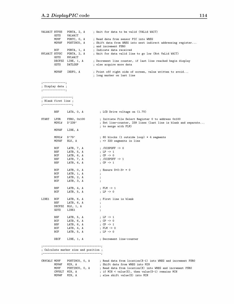
A.2 DisplayPIC code 114
VALWAIT BTFSS PORTA, 2, A ; Wait for data to be valid (VALid WAIT)
GOTO VALWAIT
MOVF PORTC, 0, A ; Read data from sensor PIC into WREG
MOVWF POSTINC0, A ; Shift data from WREG into next indirect addressing register...
; and increment FSR0
BCF PORTA, 1, A ; Indicate data received
NVLWAIT BTFSC PORTA, 2, A ; Wait for data valid line to go low (Not VaLid WAIT)
GOTO NVLWAIT
DECFSZ LINE, 1, A ; Decrement line counter, if last line reached begin display
GOTO DATLOOP ; else acquire more data
MOVWF INDF0, A ; Point off right side of screen, value written to avoid...
; long marker on last line
;--------------;
; Display data ;
;--------------;
;------------------;
; Blank first line ;
;------------------;
BSF LATA, 0, A ; LCD Drive voltage on (1.7V)
START LFSR FSR0, 0x100 ; Initiate File Select Register 0 to address 0x100
MOVLW D’239’ ; Set line-counter, 239 lines (last line is blank and separate...
; to merge with FLM)
MOVWF LINE, A
MOVLW D’79’ ; 80 blocks (1 outside loop) * 4 segments
MOVWF BLK, A ; => 320 segments in line
BCF LATB, 7, A ; /DISPOFF -> 0
BSF LATB, 5, A ; LP -> 1
BCF LATB, 6, A ; CP -> 0
BSF LATB, 7, A ; /DISPOFF -> 1
BSF LATB, 6, A ; CP -> 1
BCF LATB, 0, A ; Ensure D<0:3> = 0
BCF LATB, 1, A ;
BCF LATB, 2, A ;
BCF LATB, 3, A ;
BSF LATB, 4, A ; FLM -> 1
BCF LATB, 5, A ; LP -> 0
LINE1 BCF LATB, 6, A ; First line is blank
BSF LATB, 6, A ;
DECFSZ BLK, 1, A ;
GOTO LINE1 ;
BSF LATB, 5, A ; LP -> 1
BCF LATB, 6, A ; CP -> 0
BSF LATB, 6, A ; CP -> 1
BCF LATB, 4, A ; FLM -> 0
BCF LATB, 5, A ; LP -> 0
DECF LINE, 1, A ; Decrement line-counter
;------------------------------------;
; Calculate marker size and position ;
;------------------------------------;
CRVCALC MOVF POSTINC0, 0, A ; Read data from location(X-1) into WREG and increment FSR0
MOVWF MIN, A ; Shift data from WREG into MIN
MOVF POSTINC0, 0, A ; Read data from location(X) into WREG and increment FSR0
CPFSLT MIN, A ; if MIN < value(X), then value(X-1) remains MIN
MOVWF MIN, A ; else shift value(X) into MIN

A.2 DisplayPIC code 115
MOVWF MAX, A ; Shift value(X) into MAX
MOVF POSTDEC0, 0, A ; Read data from location X+1 into WREG and decrement FSR0
CPFSLT MIN, A ; if MIN < value(X+1), then MIN is unchanged
MOVWF MIN, A ; else shift value(X+1) into MIN
MOVF MIN, 0, A ; Shift value(MIN) into WREG
CPFSGT MAX, A ; if MAX > WREG, then increment value(MIN) by 1
GOTO NODIAG ; else GOTO NODIAG
INCF MIN, 1, A ;
NODIAG MOVF MIN, 0, A ; Shift value(MIN)...
MOVWF BLK, A ; ...into BLK
RRNCF BLK, 1, A ; Divide by four (round down), writing in blocks of 4 pixels
RRNCF BLK, 1, A ;
BCF BLK, 7, A ;
BCF BLK, 6, A ; => BLK = number of blocks to minimum of current and adjacent rows
MOVF MAX, 0, A ; Shift value(MAX)...
MOVWF BLK2, A ; ...into BLK2
RRNCF BLK2, 1, A ; Divide by four (round down), writing in blocks of 4 pixels
RRNCF BLK2, 1, A ;
BCF BLK2, 7, A ;
BCF BLK2, 6, A ; => BLK2 = number of blocks to max of current and adjacent rows
MOVLW D’78’ ; Preload BLK3 with 78 (80 blocks total, 78 either light or dark,...
MOVWF BLK3, A ; ...2 possible partially lit blocks at top and bottom of marker)
MOVF BLK2, 0, A ; Subtract value(MAX)/4 from BLK3
SUBWF BLK3, 1, A ; => BLK3 = num of blocks between current intensity, and end of row
MOVF BLK, 0, A ; Subtract BLK from BLK2
SUBWF BLK2, 1, A ; => BLK2 = number of blocks between current intensity value...
INCF BLK2, 1, A ; ...and min of current and adjacent values
MOVF BLK, 0, A
;--------------------------------;
; Test for delay increase signal ;
;--------------------------------;
BTFSS PORTA 3, A
CALL KEEPDEL
BTFSC PORTA, 3, A
CALL CYCLICDELAY
;----------------------------;
; Address pixels under curve ;
;----------------------------;
NORM BSF LATB, 0, A ; Ensure D<0:3> = 1
BSF LATB, 1, A ;
BSF LATB, 2, A ;
BSF LATB, 3, A ;
TSTFSZ BLK, A ; Avoid decrement to 255 on zero value
GOTO BLANK1B
GOTO SKIP1B
BLANK1B BCF LATB, 6, A ; value(BLK) number of display clock cycles
BSF LATB, 6, A ;
DECFSZ BLK, 1, A ;
GOTO BLANK1B ;
SKIP1B BCF MIN, 7, A ; MIN -> (MIN mod 4)
BCF MIN, 6, A ; Determine number of bright pixels in first block of marker
BCF MIN, 5, A ;
BCF MIN, 4, A ;
BCF MIN, 3, A ;
BCF MIN, 2, A ;
DECF MIN, 1, A ; Decrement MIN four times

A.2 DisplayPIC code 116
DECF MIN, 1, A ; => can count *up* to zero
DECF MIN, 1, A ;
DECF MIN, 1, A ;
BCF MAX, 7, A ; MAX -> (MAX mod 4)
BCF MAX, 6, A ; Determine number of dark pixels in last block of marker
BCF MAX, 5, A ;
BCF MAX, 4, A ;
BCF MAX, 3, A ;
BCF MAX, 2, A ;
DECF MAX, 1, A ; Decrement MAX four times
DECF MAX, 1, A ; => can count *up* to zero
DECF MAX, 1, A ;
DECF MAX, 1, A ;
;---------------------------------------;
; Find where in a block the mark begins ;
;---------------------------------------;
BCF LATB, 0, A ; D0 -> 0
INFSNZ MIN, 1, A ; Increment MIN, if MIN cycles to zero...
GOTO MARK ; ...then goto MARK
BCF LATB, 1, A ; D1 -> 0
INFSNZ MIN, 1, A ; Increment MIN, if MIN cycles to zero...
GOTO MARK ; ...then goto MARK
BCF LATB, 2, A ; D2 -> 0
INFSNZ MIN, 1, A ; Increment MIN, if MIN cycles to zero...
GOTO MARK ; ...then goto MARK
BCF LATB, 3, A ; D3 -> 0
;----------------------;
; Place marker on line ;
;----------------------;
MARK MOVLW D’1’
CPFSEQ BLK2, A
GOTO MID
INFSNZ MAX, 1, A
GOTO MID
BSF LATB, 0, A
INFSNZ MAX, 1, A
GOTO MID
BSF LATB, 1, A
INFSNZ MAX, 1, A
GOTO MID
BSF LATB, 2, A
MID BCF LATB, 6, A ; CP -> 0
BSF LATB, 6, A ; CP -> 1
BCF LATB, 3, A ; D<0:3> -> 1
BCF LATB, 2, A ;
BCF LATB, 1, A ;
BCF LATB, 0, A ;
DECFSZ BLK2, 1, A
GOTO MARK
BSF LATB, 0, A ; Ensure D<0:3> = 1
BSF LATB, 1, A ;
BSF LATB, 2, A ;
BSF LATB, 3, A ;
TSTFSZ BLK3, A ; Avoid decrement to 255 on zero value
GOTO BLANK1C
GOTO SKIP1C
BLANK1C BCF LATB, 6, A ; Following BLK2 blocks are blue (D=0)
BSF LATB, 6, A ;
DECFSZ BLK3, 1, A ;
GOTO BLANK1C ;

A.2 DisplayPIC code 117
SKIP1C BSF LATB, 5, A ; LP -> 1
BCF LATB, 6, A ; CP -> 0
BSF LATB, 6, A ; CP -> 1
BCF LATB, 5, A ; LP -> 0
DECFSZ LINE, 1, A ; Move on to next line
GOTO CRVCALC
MOVLW D’79’ ; 80 blocks (1 outside loop) * 4 segments
MOVWF BLK, A ; => 320 segments in line
BCF LATB, 0, A ; Ensure D<0:3> = 0
BCF LATB, 1, A ;
BCF LATB, 2, A ;
BCF LATB, 3, A ;
BLANK1D BCF LATB, 6, A ; Last line is blank
BSF LATB, 6, A ;
DECFSZ BLK, 1, A ;
GOTO BLANK1D ;
DECFSZ FCOUNT, 1, A ; Decrement FrameCount, if FrameCount /= 0
GOTO START ; then repeat frame
GOTO GETDATA ; else acquire new frame of data from SensorPIC
;-------------------------;
; Cyclic delay subroutine ;
;-------------------------;
CYCLICDELAY INCFSZ SLOW, 1, A ; Increment SLOW, if cycle from 0xFF to 0x00 skip an instruction
GOTO POSTINC
INCF SLOW2, 1, A ; Increment SLOW2
BTFSS SLOW2, 1, A ; if SLOW2 == 2, skip next instruction
GOTO POSTINC
CLRF SLOW2, A ; Set SLOW2 = 0
CLRF SLOW, A ; Set SLOW = 0
INCF CYCDL, 1, A ; Increment CYCDL
MOVLW D’255’
CPFSGT CYCDL, A
GOTO POSTINC
MOVLW D’1’
MOVWF CYCDL, A
POSTINC INCF CYCDL, 1, A ; if CYCDL == 0
DCFSNZ CYCDL, 1, A ;
INCF CYCDL, 1, A ; then increment CYCDL
MOVF CYCDL, 0, A ; Shift CYCDL...
MOVWF TIME1, A ; ...into TIME1
MDLOOP1 NOP ; Delay-loop, count down from CYCDL to zero
NOP
NOP
DECFSZ TIME1, 1, A
GOTO MDLOOP1
RETURN
KEEPDEL INCF CYCDL, 1, A ; if CYCDL == 0
DCFSNZ CYCDL, 1, A ;
INCF CYCDL, 1, A ; then increment CYCDL
MOVF CYCDL, 0, A ; Shift CYCDL...
MOVWF TIME1, A ; ...into TIME1
MDLOOP2 NOP ; Delay-loop, count down from CYCDL to zero
NOP
NOP
DECFSZ TIME1, 1, A
GOTO MDLOOP2
RETURN

A.2 DisplayPIC code 118
;----------------------------------;
; Long delay subroutine (~0.978 s) ;
;----------------------------------;
LONGDELAY MOVLW D’10’
MOVWF TIME1, A
LDLOOP1 MOVLW D’255’
MOVWF TIME2, A
LDLOOP2 MOVLW D’255’
MOVWF TIME3, A
LDLOOP3 DECFSZ TIME3, 1, A
GOTO LDLOOP3
DECFSZ TIME2, 1, A
GOTO LDLOOP2
DECFSZ TIME1, 1, A
GOTO LDLOOP1
RETURN
END

Appendix B
Deriving the Hamiltonian for the
Time-Dependent Adiabatic State
We start with the time-dependent Schrodinger equation for the diabatic state
id
dt|ψ〉 = H|ψ〉 (B.1)
The adiabatic state is given by the unitary transformation
|φ〉 = U|ψ〉 (B.2)
Which allows us to make the substitution for the diabatic state
|ψ〉 = U−1|φ〉 (B.3)
⇒ id
dt
(U|φ〉
)= HU|φ〉 (B.4)
⇒ i
(d
dtU
)|φ〉 + U
d|φ〉dt
= HU|φ〉 (B.5)

120
The time-dependent Schrodinger equation for the adiabatic state is given by
id
dt|φ〉 = HA|φ〉 (B.6)
⇒ d
dt|φ〉 =
1
iHA|φ〉 (B.7)
Substituting this into equation B.5 gives
i
(d
dtU
)|φ〉 + UHA|φ〉 = HU|φ〉 (B.8)
Multiplying both sides by U−1 and rearranging in terms of HA gives
HA|φ〉 =
(U−1HU− iU−1 d
dtU
)|φ〉 (B.9)
which is the Hamiltonian for the time–dependent adiabatic state
HA = U−1HU− iU−1 d
dtU (B.10)

Appendix C
Adiabatic Theorem MATLAB
Code
C.1 Analyzing the effect of differing field profilesclear; clc; clf;
%%%%%%%%%%%%%%%%%%%%%%%%%%%%%%%%%%%%%%%%%%%%%%%%%%%%%%%%%%%%%%%%%%%%%%%%
% Solving the amplitude equations quantum system near a curve crossing %
% for different field profiles %
%%%%%%%%%%%%%%%%%%%%%%%%%%%%%%%%%%%%%%%%%%%%%%%%%%%%%%%%%%%%%%%%%%%%%%%%
nosteps = 4001; % Number of time-steps
N = (nosteps - 1)/2; % Time runs from -tmax -> tmax
tmax = 4;
dt = tmax/N; % Stepsize
a = 1; % Coupling between diabatic states
hbar = 1;
t(1) = -tmax; % Initial time
cA1(1) = sqrt(1); % Initial amplitude of adiabatic state 1
cA2(1) = sqrt(0); % Initial amplitude of adiabatic state 2
E0(1) = 0; % Initial value of ea0.dF/dt
E0max = 30; % Maximum value of ea0.dF/dt
Fmax = E0max/2*(2*tmax + dt); % Maximum electric field
F(1) = -Fmax/2; % Initial electric field
epsilon(1) = sqrt(E0max/2^2*t(1)^2 + a^2); % Initial adiabatic state energy
w0 = 2*epsilon(1)/hbar; % Initial frequency splitting
figure(1) % Create figure
for q = 1:3
for n = 2:nosteps
t(n) = t(n-1) + dt; % Time
if q == 1 % Linear field ramp
F(n) = F(n-1) + E0max/2*dt;
elseif q == 2 % sin^2 field ramp
F(n) = Fmax*sin(pi/(4*tmax)*(t(n) + tmax))^2 - Fmax/2;

C.1 Analyzing the effect of differing field profiles 122
elseif q == 3
if t(n) < 0 % First sin^2 field ramp
F(n) = Fmax/2*sin(pi/(2*tmax)*(t(n) + tmax))^2 - Fmax/2;
else % Second sin^2 field ramp
F(n) = Fmax/2*sin(pi/(2*tmax)*t(n))^2 + Fmax/2 - Fmax/2;
end
end
E0(n) = (F(n) - F(n-1))/dt; % Field gradiant
epsilon(n) = sqrt(F(n)^2 + a^2); % Adiabatic state energy
gamma(n) = a*E0max/2/(2*epsilon(n)^2); % Coupling between adiabatic states
% 4th order Runge-Kutta solution algorithm
p1 = i*epsilon(n-1)*cA1(n-1) - gamma(n-1)*cA2(n-1);
q1 = gamma(n-1)*cA1(n-1) - i*epsilon(n-1)*cA2(n-1);
p2 = i*epsilon(n-1)*(cA1(n-1) + dt/2*p1) - gamma(n-1)*(cA2(n-1) + dt/2*q1);
q2 = gamma(n-1)*(cA1(n-1) + dt/2*p1) - i*epsilon(n-1)*(cA2(n-1) + dt/2*q1);
p3 = i*epsilon(n-1)*(cA1(n-1) + dt/2*p2) - gamma(n-1)*(cA2(n-1) + dt/2*q2);
q3 = gamma(n-1)*(cA1(n-1) + dt/2*p2) - i*epsilon(n-1)*(cA2(n-1) + dt/2*q2);
p4 = i*epsilon(n-1)*(cA1(n-1) + dt*p3) - gamma(n-1)*(cA2(n-1) + dt*q3);
q4 = gamma(n-1)*(cA1(n-1) + dt*p3) - i*epsilon(n-1)*(cA2(n-1) + dt*q3);
cA1(n) = cA1(n-1) + dt/6*(p1 + 2*p2 + 2*p3 + p4);
cA2(n) = cA2(n-1) + dt/6*(q1 + 2*q2 + 2*q3 + q4);
end
subplot(3,3,q);plot(t,F,’k-’,’linewidth’,2)
axis([-tmax tmax -Fmax/2 Fmax/2])
if q == 1
ylabel(’Field strength’,’fontsize’,16)
title(’(a)’,’fontsize’,16)
elseif q == 2
title(’(b)’,’fontsize’,16)
else
title(’(c)’,’fontsize’,16)
end
subplot(3,3,q+3);plot(t(2:n),-epsilon(2:n),’r-’,t(2:n),epsilon(2:n),’b-’,’linewidth’,2)
axis([-tmax tmax -70 70])
if q == 1
ylabel(’Energy’,’fontsize’,16)
end
subplot(3,3,q+6);plot(t,cA1.*conj(cA1),’r-’,t,cA2.*conj(cA2),’b-’,’linewidth’,2)
text(-3.6,0.45,sprintf(’P_diabatic = %1.2f’,cA2(n)*conj(cA2(n))))
if q == 1
xlabel(’Time’,’fontsize’,16)
ylabel(’Populations’,’fontsize’,16)
else
xlabel(’Time’,’fontsize’,16)
end
end

C.2 Comparing numerical results with calculations using theLandau–Zener formula 123
C.2 Comparing numerical results with calculations
using the Landau–Zener formulaclear; clc; clf;
%%%%%%%%%%%%%%%%%%%%%%%%%%%%%%%%%%%%%%%%%%%%%%%%%%%%%%%%%%%%%%%%%%%%%%%%
% Solving the amplitude equations quantum system near a curve crossing %
% comparison of numerical results with Landau-Zener %
%%%%%%%%%%%%%%%%%%%%%%%%%%%%%%%%%%%%%%%%%%%%%%%%%%%%%%%%%%%%%%%%%%%%%%%%
nosteps = 4001; % Number of time-steps
N = (nosteps - 1)/2; % Time runs from -tmax -> tmax
tmax = 4;
dt = tmax/N; % Stepsize
num = 20; % Number of values of ea0.dF/dt
E0min = 1; % Minimum value of ea0.dF/dt
E0max = 30; % Maximum value of ea0.dF/dt
a = 1; % Coupling between diabatic states
hbar = 1;
t(1) = -tmax; % Initial time
cA1(1) = sqrt(1); % Initial amplitude of adiabatic state 1
cA2(1) = sqrt(0); % Initial amplitude of adiabatic state 1
for q = 1:num
E0(q) = E0min + (q-1)*(E0max - E0min)/num; % Electric field gradient
epsilon(1) = sqrt(E0(q)^2*t(1)^2 + a^2); % Initial adiabatic energy
for n = 2:nosteps
t(n) = t(n-1) + dt; % Time
F(q,n) = E0(q)*(t(n) + tmax + dt); % Electric field strength
epsilon(n) = sqrt(E0(q)^2*t(n)^2 + a^2); % Adiabatic state energy
gamma(n) = a*E0(q)/2/epsilon(n)^2; % Coupling between adiabatic states
% 4th order Runge-Kutta solution algorithm
p1 = i*epsilon(n-1)*cA1(n-1) - gamma(n-1)*cA2(n-1);
q1 = gamma(n-1)*cA1(n-1) - i*epsilon(n-1)*cA2(n-1);
p2 = i*epsilon(n-1)*(cA1(n-1) + dt/2*p1) - gamma(n-1)*(cA2(n-1) + dt/2*q1);
q2 = gamma(n-1)*(cA1(n-1) + dt/2*p1) - i*epsilon(n-1)*(cA2(n-1) + dt/2*q1);
p3 = i*epsilon(n-1)*(cA1(n-1) + dt/2*p2) - gamma(n-1)*(cA2(n-1) + dt/2*q2);
q3 = gamma(n-1)*(cA1(n-1) + dt/2*p2) - i*epsilon(n-1)*(cA2(n-1) + dt/2*q2);
p4 = i*epsilon(n-1)*(cA1(n-1) + dt*p3) - gamma(n-1)*(cA2(n-1) + dt*q3);
q4 = gamma(n-1)*(cA1(n-1) + dt*p3) - i*epsilon(n-1)*(cA2(n-1) + dt*q3);
cA1(n) = cA1(n-1) + dt/6*(p1 + 2*p2 + 2*p3 + p4);
cA2(n) = cA2(n-1) + dt/6*(q1 + 2*q2 + 2*q3 + q4);
end
if q == 5
figure(1) % Plot adiabatic state populations
axes(’fontsize’,20)
plot(t,cA1.*conj(cA1),’r-’,t,cA2.*conj(cA2),’b-’,’linewidth’,2)
legend(’\rho^A_11(t)’,’\rho^A_22(t)’)
xlabel(’Time’)
figure(2) % Plot adiabatic state energies
axes(’fontsize’,20)
plot(t,-epsilon,’r-’,t,epsilon,’b-’,’linewidth’,2)
legend(’\it\epsilon_1’,’\it\epsilon_2’)

C.2 Comparing numerical results with calculations using theLandau–Zener formula 124
xlabel(’Time’)
ylabel(’Energy’)
end
% Numerical solution for probability of a diabatic transition
nonadiabaticpop(q) = cA2(n)*conj(cA2(n));
% Landau-Zener value for probability of a diabatic transition (shifted)
PLZ(q) = exp(-2*pi*a^2/(hbar*2*(E0(q) - 0.005))) - 0.005;
end
figure(3) % Compare numerical results with Landau-Zener
axes(’fontsize’,16)
plot(E0,nonadiabaticpop,’b-’,E0,PLZ,’r-’,’linewidth’,2)
legend(’Numerical calculation’,’Landau-Zener (shifted by 0.005 \itx and \it-y)’)
xlabel(’Field gradient’,’fontsize’,20)
ylabel(’Diabatic transition probability’,’fontsize’,20)

Appendix D
MATLAB Simulation of Population
Dynamics in a 4–Level System
clear; clc; clf;
%%%%%%%%%%%%%%%%%%%%%%%%%%%%%%%%%%%%%%%%%%%%%%%%%%%%%%%%%%%%%%%%%%%
%% Population dynamics of a 4-level ’double lambda’ system %%
%% 4 light fields with variable frequency, intensity and phase %%
%%%%%%%%%%%%%%%%%%%%%%%%%%%%%%%%%%%%%%%%%%%%%%%%%%%%%%%%%%%%%%%%%%%
e = 1.6e-19; hbar = 1.05e-34; c = 3e8; % Fundamental constants
a0 = 0.5292e-10; ep0 = 8.85e-12;
h0 = 2e-10; % Stepsize
notimesteps = 25000; % Number of timesteps
tmax = 2e-6; % Simulation running time
tcoll = 0.5e-6; % Interval between collisions
dephase = 0; % 1 = collisions on
numden = 1e19; % Atomic number density
% Level frequencies
% (define |1> as zero)
lev(1) = 0;
lev(2) = 2*pi*806e6;
lev(3) = 2*pi*446810e9;
lev(4) = 2*pi*446810.094e9;
% Frequency splittings
w = zeros(4,4);
for k = 1:4
for l = 1:4
w(k,l) = lev(k) - lev(l);
end
end
% 4 Laser frequencies
wL = zeros(4,4);
wL(1,3) = w(3,1);
wL(2,3) = w(3,2);
wL(1,4) = w(4,1);
wL(2,4) = w(4,2);
% Detunings
Delta = zeros(4,4);
for k = 1:4
for l = 1:4

126
for m = 1:4
for n = 1:4
Delta(k,l,m,n) = wL(k,l) - w(m,n);
end
end
end
end
% Initial phases of light fields
phi13 = 0;
phi14 = 0;
phi23 = 0;
phi24 = 0;
% Relaxation rates of states |3> and |4>
Gamma3 = 1e7;
Gamma4 = 1e8;
% Electric field amplitude of light fields
E = zeros(4,4);
E(1,3) = 1000;
E(2,3) = 1000;
E(1,4) = 0;
E(2,4) = 0;
% Initial transition dipole moments
D = zeros(4,4);
r = 0;
for k = 2:4
r = r + 1;
for l = 1:r
D(k,l) = -e*a0;
D(l,k) = conj(D(k,l));
end
end
d(:,:) = D(:,:);
% Initial Rabi frequencies
for k = 1:4
for l = 1:4
for m = 1:4
for n = 1:4
Chi(k,l,m,n) = -D(k,l)*E(m,n)/hbar;
end
end
end
end
Chi(4,2,2,3) = -Chi(3,2,2,3);
% Define solution matrix
v = zeros(notimesteps,6);
% Initial amplitudes
v(1,2) = 1;
v(1,3) = 0;
%v(1,4) = 1/sqrt(2);
%v(1,5) = 1/sqrt(2);
v(1,6) = 1;
% Initial absorption coefficient
Kappa(1) = (wL(1,3)/c)*2*numden/(ep0*E(1,3))*imag(v(1,2)*conj(v(1,4))*D(3,1));
% Baseline for measuring collision interval
T = 0;
for n = 2:notimesteps

127
% Time
v(n,1) = v(n-1,1) + h0;
% t = tmax -> end simulation
if v(n,1) > tmax
fprintf(1,’t > tmax’)
break
end
% Collisional dephasing
if dephase == 1
if v(n,1) > T + tcoll
fprintf(1,’Collision, t = %1.2f us\n’,1e6*v(n,1))
T = T + tcoll;
% Dephase transition dipole moments, d(i,j) = d(j,i)^*
R = rand(4,1);
r = 0;
for k = 2:4
r = r + 1;
for l = 1:r
d(k,l) = D(k,l)*exp(i*2*pi*(R(l) - R(k)));
d(l,k) = conj(d(k,l));
end
end
% Re-define Rabi frequencies
for k = 1:4
for l = 1:4
for m = 1:2
for p = 3:4
Chi(k,l,m,p) = -d(k,l)*E(m,p)/hbar;
end
end
end
end
end
end
% 4th order Runge-Kutta solution algorithm
p1 = -i/2*((conj(Chi(3,1,1,3))*exp(i*(Delta(1,3,3,1)*v(n-1,1) + phi13)) +...
conj(Chi(3,1,1,4))*exp(i*(Delta(1,4,3,1)*v(n-1,1) + phi14)))*v(n-1,4) +...
(conj(Chi(4,1,1,3))*exp(i*(Delta(1,3,4,1)*v(n-1,1) + phi13)) +...
conj(Chi(4,1,1,4))*exp(i*(Delta(1,4,4,1)*v(n-1,1) + phi14)))*v(n-1,5));
q1 = -i/2*((conj(Chi(3,2,2,3))*exp(i*(Delta(2,3,3,2)*v(n-1,1) + phi23)) +...
conj(Chi(3,2,2,4))*exp(i*(Delta(2,4,3,2)*v(n-1,1) + phi24)))*v(n-1,4) +...
(conj(Chi(4,2,2,3))*exp(i*(Delta(2,3,4,2)*v(n-1,1) + phi23)) +...
conj(Chi(4,2,2,4))*exp(i*(Delta(2,4,4,2)*v(n-1,1) + phi24)))*v(n-1,5));
r1 = -i/2*((Chi(3,1,1,3)*exp(-i*(Delta(1,3,3,1)*v(n-1,1) + phi13)) +...
Chi(3,1,1,4)*exp(-i*(Delta(1,4,3,1)*v(n-1,1) + phi14)))*v(n-1,2) +...
(Chi(3,2,2,3)*exp(-i*(Delta(2,3,3,2)*v(n-1,1) + phi23)) +...
Chi(3,2,2,4)*exp(-i*(Delta(2,4,3,2)*v(n-1,1) + phi24)))*v(n-1,3)) - Gamma3/2*v(n-1,4);
s1 = -i/2*((Chi(4,1,1,3)*exp(-i*(Delta(1,3,4,1)*v(n-1,1) + phi13)) +...
Chi(4,1,1,4)*exp(-i*(Delta(1,4,4,1)*v(n-1,1) + phi14)))*v(n-1,2) +...
(Chi(4,2,2,3)*exp(-i*(Delta(2,3,4,2)*v(n-1,1) + phi23)) +...
Chi(4,2,2,4)*exp(-i*(Delta(2,4,4,2)*v(n-1,1) + phi24)))*v(n-1,3)) - Gamma4/2*v(n-1,5);
p2 = -i/2*((conj(Chi(3,1,1,3))*exp(i*(Delta(1,3,3,1)*(v(n-1,1) + h0/2) + phi13)) +...
conj(Chi(3,1,1,4))*exp(i*(Delta(1,4,3,1)*(v(n-1,1) + h0/2) + phi14)))*(v(n-1,4) + h0/2*r1) +...
(conj(Chi(4,1,1,3))*exp(i*(Delta(1,3,4,1)*(v(n-1,1) + h0/2) + phi13)) +...
conj(Chi(4,1,1,4))*exp(i*(Delta(1,4,4,1)*(v(n-1,1) + h0/2) + phi14)))*(v(n-1,5) + h0/2*s1));
q2 = -i/2*((conj(Chi(3,2,2,3))*exp(i*(Delta(2,3,3,2)*(v(n-1,1) + h0/2) + phi23)) +...

128
conj(Chi(3,2,2,4))*exp(i*(Delta(2,4,3,2)*(v(n-1,1) + h0/2) + phi24)))*(v(n-1,4) + h0/2*r1) +...
(conj(Chi(4,2,2,3))*exp(i*(Delta(2,3,4,2)*(v(n-1,1) + h0/2) + phi23)) +...
conj(Chi(4,2,2,4))*exp(i*(Delta(2,4,4,2)*(v(n-1,1) + h0/2) + phi24)))*(v(n-1,5) + h0/2*s1));
r2 = -i/2*((Chi(3,1,1,3)*exp(-i*(Delta(1,3,3,1)*(v(n-1,1) + h0/2) + phi13)) +...
Chi(3,1,1,4)*exp(-i*(Delta(1,4,3,1)*(v(n-1,1) + h0/2) + phi14)))*(v(n-1,2) + h0/2*p1) +...
(Chi(3,2,2,3)*exp(-i*(Delta(2,3,3,2)*(v(n-1,1) + h0/2) + phi23)) +...
Chi(3,2,2,4)*exp(-i*(Delta(2,4,3,2)*(v(n-1,1) + h0/2) + phi24)))*(v(n-1,3) + h0/2*q1)) -...
Gamma3/2*(v(n-1,4) + h0/2*r1);
s2 = -i/2*((Chi(4,1,1,3)*exp(-i*(Delta(1,3,4,1)*(v(n-1,1) + h0/2) + phi13)) +...
Chi(4,1,1,4)*exp(-i*(Delta(1,4,4,1)*(v(n-1,1) + h0/2) + phi14)))*(v(n-1,2) + h0/2*p1) +...
(Chi(4,2,2,3)*exp(-i*(Delta(2,3,4,2)*(v(n-1,1) + h0/2) + phi23)) +...
Chi(4,2,2,4)*exp(-i*(Delta(2,4,4,2)*(v(n-1,1) + h0/2) + phi24)))*(v(n-1,3) + h0/2*q1)) -...
Gamma4/2*(v(n-1,5) + h0/2*s1);
p3 = -i/2*((conj(Chi(3,1,1,3))*exp(i*(Delta(1,3,3,1)*(v(n-1,1) + h0/2) + phi13)) +...
conj(Chi(3,1,1,4))*exp(i*(Delta(1,4,3,1)*(v(n-1,1) + h0/2) + phi14)))*(v(n-1,4) + h0/2*r2) +...
(conj(Chi(4,1,1,3))*exp(i*(Delta(1,3,4,1)*(v(n-1,1) + h0/2) + phi13)) +...
conj(Chi(4,1,1,4))*exp(i*(Delta(1,4,4,1)*(v(n-1,1) + h0/2) + phi14)))*(v(n-1,5) + h0/2*s2));
q3 = -i/2*((conj(Chi(3,2,2,3))*exp(i*(Delta(2,3,3,2)*(v(n-1,1) + h0/2) + phi23)) +...
conj(Chi(3,2,2,4))*exp(i*(Delta(2,4,3,2)*(v(n-1,1) + h0/2) + phi24)))*(v(n-1,4) + h0/2*r2) +...
(conj(Chi(4,2,2,3))*exp(i*(Delta(2,3,4,2)*(v(n-1,1) + h0/2) + phi23)) +...
conj(Chi(4,2,2,4))*exp(i*(Delta(2,4,4,2)*(v(n-1,1) + h0/2) + phi24)))*(v(n-1,5) + h0/2*s2));
r3 = -i/2*((Chi(3,1,1,3)*exp(-i*(Delta(1,3,3,1)*(v(n-1,1) + h0/2) + phi13)) +...
Chi(3,1,1,4)*exp(-i*(Delta(1,4,3,1)*(v(n-1,1) + h0/2) + phi14)))*(v(n-1,2) + h0/2*p2) +...
(Chi(3,2,2,3)*exp(-i*(Delta(2,3,3,2)*(v(n-1,1) + h0/2) + phi23)) +...
Chi(3,2,2,4)*exp(-i*(Delta(2,4,3,2)*(v(n-1,1) + h0/2) + phi24)))*(v(n-1,3) + h0/2*q2)) -...
Gamma3/2*(v(n-1,4) + h0/2*r2);
s3 = -i/2*((Chi(4,1,1,3)*exp(-i*(Delta(1,3,4,1)*(v(n-1,1) + h0/2) + phi13)) +...
Chi(4,1,1,4)*exp(-i*(Delta(1,4,4,1)*(v(n-1,1) + h0/2) + phi14)))*(v(n-1,2) + h0/2*p2) +...
(Chi(4,2,2,3)*exp(-i*(Delta(2,3,4,2)*(v(n-1,1) + h0/2) + phi23)) +...
Chi(4,2,2,4)*exp(-i*(Delta(2,4,4,2)*(v(n-1,1) + h0/2) + phi24)))*(v(n-1,3) + h0/2*q2)) -...
Gamma4/2*(v(n-1,5) + h0/2*s2);
p4 = -i/2*((conj(Chi(3,1,1,3))*exp(i*(Delta(1,3,3,1)*(v(n-1,1) + h0) + phi13)) +...
conj(Chi(3,1,1,4))*exp(i*(Delta(1,4,3,1)*(v(n-1,1) + h0) + phi14)))*(v(n-1,4) + h0*r3) +...
(conj(Chi(4,1,1,3))*exp(i*(Delta(1,3,4,1)*(v(n-1,1) + h0) + phi13)) +...
conj(Chi(4,1,1,4))*exp(i*(Delta(1,4,4,1)*(v(n-1,1) + h0) + phi14)))*(v(n-1,5) + h0*s3));
q4 = -i/2*((conj(Chi(3,2,2,3))*exp(i*(Delta(2,3,3,2)*(v(n-1,1) + h0) + phi23)) +...
conj(Chi(3,2,2,4))*exp(i*(Delta(2,4,3,2)*(v(n-1,1) + h0) + phi24)))*(v(n-1,4) + h0*r3) +...
(conj(Chi(4,2,2,3))*exp(i*(Delta(2,3,4,2)*(v(n-1,1) + h0) + phi23)) +...
conj(Chi(4,2,2,4))*exp(i*(Delta(2,4,4,2)*(v(n-1,1) + h0) + phi24)))*(v(n-1,5) + h0*s3));
r4 = -i/2*((Chi(3,1,1,3)*exp(-i*(Delta(1,3,3,1)*(v(n-1,1) + h0) + phi13)) +...
Chi(3,1,1,4)*exp(-i*(Delta(1,4,3,1)*(v(n-1,1) + h0) + phi14)))*(v(n-1,2) + h0*p3) +...
(Chi(3,2,2,3)*exp(-i*(Delta(2,3,3,2)*(v(n-1,1) + h0) + phi23)) +...
Chi(3,2,2,4)*exp(-i*(Delta(2,4,3,2)*(v(n-1,1) + h0) + phi24)))*(v(n-1,3) + h0*q3)) -...
Gamma3/2*(v(n-1,4) + h0*r3);
s4 = -i/2*((Chi(4,1,1,3)*exp(-i*(Delta(1,3,4,1)*(v(n-1,1) + h0) + phi13)) +...
Chi(4,1,1,4)*exp(-i*(Delta(1,4,4,1)*(v(n-1,1) + h0) + phi14)))*(v(n-1,2) + h0*p3) +...
(Chi(4,2,2,3)*exp(-i*(Delta(2,3,4,2)*(v(n-1,1) + h0) + phi23)) +...
Chi(4,2,2,4)*exp(-i*(Delta(2,4,4,2)*(v(n-1,1) + h0) + phi24)))*(v(n-1,3) + h0*q3)) -...
Gamma4/2*(v(n-1,5) + h0*s3);
%%% |psi> = c1|1> + c2|2> + c3|3> + c4|4> %%%
% c1
v(n,2) = v(n-1,2) + h0/6*(p1 + 2*p2 + 2*p3 + p4);
% c2
v(n,3) = v(n-1,3) + h0/6*(q1 + 2*q2 + 2*q3 + q4);
% c3
v(n,4) = v(n-1,4) + h0/6*(r1 + 2*r2 + 2*r3 + r4);
% c4

129
v(n,5) = v(n-1,5) + h0/6*(s1 + 2*s2 + 2*s3 + s4);
% Total system population
v(n,6) = abs(v(n,2))^2 + abs(v(n,3))^2 + abs(v(n,4))^2 + abs(v(n,5))^2;
% Absorption coefficient
Kappa(n) = (wL(1,3)/c)*2*numden/(ep0*E(1,3))*imag(conj(v(n,2))*v(n,4)*d(3,1));
end
% Define output variables from solution matrix
t = v(1:n-1,1);
c1 = v(1:n-1,2);
c2 = v(1:n-1,3);
c3 = v(1:n-1,4);
c4 = v(1:n-1,5);
c1234 = v(1:n-1,6);
% Plot level populations
figure(1)
axes(’fontsize’,30)
plot(t*1e6,abs(c1).^2,’k-’,t*1e6,abs(c2).^2,’r-’,t*1e6,abs(c3).^2,’b-’,t*1e6,abs(c4).^2,’g-’,’linewidth’,2)
legend(’\rho_11’,’\rho_22’,’\rho_33’,’\rho_44’)
axis([0 tmax*1e6 0 1])
title(’4-level system, antisymmetric phase’)%,’fontsize’,18)
xlabel(’Time [\mus]’)%,’fontsize’,18)
% Plot total system population
figure(2)
axes(’fontsize’,16)
plot(t*1e6,c1234,’k-’);
title(’Tr[\rho]’);
xlabel(’Time [\mus]’)
% Plot absorption coefficient
figure(3)
axes(’fontsize’,16)
plot(t*1e6,Kappa(1:n-1),’k-’)
title(’Absorption coefficient’)
xlabel(’Time [\mus]’)
ylabel(’\kappa [m^-1]’)