development of non-nb coatings for srf accelerator cavities alex gurevich old dominion university,...
TRANSCRIPT

Development of non-Nb coatings for SRF accelerator cavities
Alex Gurevich
Old Dominion University,Department of Physics and Center for Accelerator Science,
Norfolk, VA 23529, USA
Future Circular Collider Study, Washington DC, March 24, 2015
Supported by DOE under grant No. DE-SC0010081
Why new SRF materials are needed?
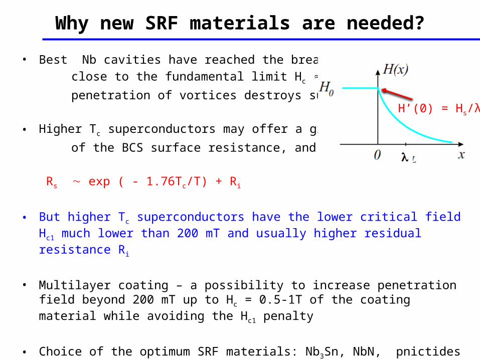
• Best Nb cavities have reached the breakdown fields close to the fundamental limit Hc 200 mT at which
penetration of vortices destroys superconductivity.
• Higher Tc superconductors may offer a great reduction
of the BCS surface resistance, and higher Q:
Rs exp ( - 1.76Tc/T) + Ri
• But higher Tc superconductors have the lower critical field Hc1 much lower than 200 mT and usually higher residual resistance Ri
• Multilayer coating – a possibility to increase penetration field beyond 200 mT up to Hc = 0.5-1T of the coating material while avoiding the Hc1 penalty
• Choice of the optimum SRF materials: Nb3Sn, NbN, pnictides or alloyed Nb.
• Possibility of developing high Q cavities operating at 4.2 K and high fields
H’(0) = Hs/λ

Multilayer coating
Nb
insulating layers
higher-TcSC: NbN, Nb3Sn, etc
Magnetic screening of the Nbcavity without vortex penetration
Multilayer coating of SC cavities: alternating SC and I layers with d <
The breakdown field could be increased up to the superheating field Hs of the coating: 450 mT for Nb3Sn
07.0ln
220
1 d
dHc
No thermodynamically stable parallel vortices due to the enhancement of Hc1 in thin films with d < (Abrikosov, 1964)
A. Gurevich, APL. 88, 012511 (2006)
Pushes the accelerating gradient above 100 mV/m
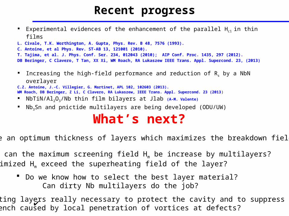
Recent progress
Experimental evidences of the enhancement of the parallel Hc1 in thin filmsL. Civale, T.K. Worthington, A. Gupta, Phys. Rev. B 48, 7576 (1993).C. Antoine, et al Phys. Rev. ST-AB 13, 121001 (2010).T. Tajima, et al. J. Phys. Conf. Ser. 234, 012043 (2010); AIP Conf. Proc. 1435, 297 (2012).DB Beringer, C Clavero, T Tan, XX Xi, WM Roach, RA Lukaszew IEEE Trans. Appl. Supercond. 23, (2013)
Increasing the high-field performance and reduction of Rs by a NbN overlayerC.Z. Antoine, J.-C. Villegier, G. Martinet, APL 102, 102603 (2013).WM Roach, DB Beringer, Z Li, C Clavero, RA Lukaszew, IEEE Trans. Appl. Supercond. 23 (2013)
NbTiN/Al2O3/Nb thin film bilayers at Jlab (A-M. Valente)
Nb3Sn and pnictide multilayers are being developed (ODU/UW)
What’s next? Is there an optimum thickness of layers which maximizes the breakdown field? ✔
If yes, how far can the maximum screening field Hm be increase by multilayers? Can the optimized Hm exceed the superheating field of the layer? ✔
Do we know how to select the best layer material? Can dirty Nb multilayers do the job? ✔
Are the insulating layers really necessary to protect the cavity and to suppress thermal quench caused by local penetration of vortices at defects? ✔

Outline
There is an optimum thickness of multilayers at which it can screen the magnetic field exceeding the superheating field of both Nb and the layer material.
MLs provide best protection of cavities against surface defects which lower the Bean-Livingston barrier and open gates for local penetration of vortices.
Dielectric layers are instrumental to suppress vortex dissipation and dendritic thermomagnetic avalanches which trigger the cavity quench.
Dielectric layers suppress thermoelectric currents which generate trapped vortices during the cavity cooldown
Implementation of the optimized Nb3Sn or NbN multilayers could double the maximum accelerating gradient, pushing it above 100 MV/m.
Pnictides could potentially quadruple the accelerating gradient.
New opportunities of using dirty Nb multilayers to push Hm up to 280-300 mT

Superheating field
Meissner state becomes unstable above the superheating field H > Hs as the current density Js = H/ at the surface reaches the depairing current density Jd = Hs/
Hs close to Tc: (Matricon and Saint-James, 1967, Chapman 1995)
Bs decreases as the surface gets dirtier and the GL parameter κ = λ/ξ increases.
Nb
At T << Tc, only Hs(0) = 0.84Hc at κ >> 1 has been calculated in the clean limit (Galaiko 1966, Catelani and Sethna, 2008)
and for arbitrary impurity concentration (Lin and Gurevich, 2012)
Surface barrier for penetration of vortices vanishes at H = Hs

Possible multilayer materials
Material Tc (K) Hc [T] Hc1 [mT] Hc2[T] [nm] [meV]
Nb 9.2 0.2 170 0.4 40 1.5
pnictides 30-55 0.5-0.9 30 >100 200 10-20
Nb3Sn 18 0.54 50 30 85 3.1
NbN 16.2 0.23 20 15 200 2.6
MgB2 40 0.43 30 3.5-60 140 2.3; 7.2
YBCO 93 1.4 10 >100 150 20
Large gap Δ (good for SRF) is usually accompanied by low Hc1 (bad for SRF)
d-wave high-Tc cuprates with nodal gap and
are not useful for SRF

Screening field in a multilayer
Solutions of London equation for a layer with the penetration depth λ on a substrate with the penetration depth λ0
Important parameters
where c and b are given by:
for the SC substrate (Nb) with λ0 < λ, both c and k are positive
J(x)
/J(0
)
Meissner state breaks down at the surface of either ML or Nb where the current densities J(0) = h’(0) and J(d) = h’(d) are maximum
T. Kubo, Y. Iwashita, and T. Saeki, APL 104, 032603 (2014); A. Gurevich, AIP Advances, 5, 017112 (2015)

Current counterflow induced by the Nb substrate
Current density in the layer J(x) = - h’(x):
Current density at the surface J(0) is reduced by the substrate with λ0 < λ:
Counterflow induced by the substrate reduces the current density at the ML surface, allowing the Meissner state in the ML to survive up to fields exceeding the bulk superheating field Hs
For a thick ML with d >> λ, the maximum field Hm is limited by Hs: at optimum thickness dm the field Hm exceeds both Hs and Hs0

Optimum thickness
The Meissner state is stable if the screening current density at the surface of both the ML and the substrate is smaller than the depairing limit:
J(0) < Jd = Hs/λ and J(d) < Jd0 = Hs0/λ0
for Hs = 2Hs0 and k = ½,dc = ln[μ + (μ2 – k)1/2 ]
The Meissner state is below both blue and red lines.
The crossing point defines the optimum thickness dm for maximum Hm which exceeds the superheating fields of both the layers and the substrate d/λ
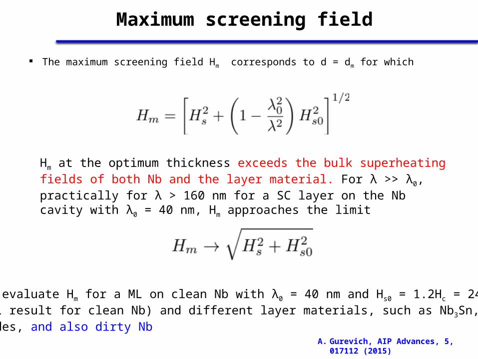
Maximum screening field
The maximum screening field Hm corresponds to d = dm for which
Hm at the optimum thickness exceeds the bulk superheating fields of both Nb and the layer material. For λ >> λ0, practically for λ > 160 nm for a SC layer on the Nb cavity with λ0 = 40 nm, Hm approaches the limit
Let us evaluate Hm for a ML on clean Nb with λ0 = 40 nm and Hs0 = 1.2Hc = 240 mT(the GL result for clean Nb) and different layer materials, such as Nb3Sn, NbN, pnictides, and also dirty Nb
A. Gurevich, AIP Advances, 5, 017112 (2015)

Estimates of Hm and dm
Nb3Sn: Hs = 0.84Hc = 454 mT and λ = 120 nm (moderately dirty):
Hm = 507 mT, dm = 1.1λ = 132 nm
doubles the superheating field of clean Nb
Ba0.6K0.4Fe2As2, Tc = 38 K, Hc = 0.9T, Hs =756 mT, λ = 200 nm
Hm = 930 mT, dm = 1.78λ = 356 nm.almost quadruples the superheating field of clean Nb
dirty Nb layer: Hc = 200 mT, Hs = 170 mT, l = 2 nm, and λ =λ(ξ0 /l)1/2 = 180 nm
Hm = 288 mT, dm = 0.44λ = 79 nm. 20% gain as compared to Hs = 240 mT of clean Nb

Can a cavity be protected only by the surface barrier?
H0
u
J])2(5.0[)( 01
/00 HHuHeHbG cv
u
H = Hc1
H < Hc1
H > Hc1
H = Hc
u
G
Thermodynamic potential G(u) as a function of the position u:
Meissner Image
• Vortices have to overcome the surface barrier even at H > Hc1 (Bean & Livingston, 1964)
• Surface barrier disappears at the overheating field H = Hs > Hc1. Meissner state is metastable at Hc1 < H < Hs
Image to ensure J┴ = 0
Inevitable surface defects weaken the surface barrier which vanishes at H = Hp where Hc1 < Hp < Hs Scanning laser confocal microscopy of a BCP Nb cavity (Jlab), P. Lee, 2006Probes ≈ 0.3-3 μm scales

Are dielectric layers really necessary?
Once a vortex breaks through a defect, it triggers penetration of avalanche of vortices causing a thermo-magnetic flux jump and the cavity quench
Poor thermal conductivity of Nb3Sn: a 2-3 μm thick film doubles the thermal impedance of the Nb cavity wall, facilitating local overheating and branching vortex avalanches
H
λλ
H
Why cannot we just deposit a thick Nb3Sn film without I layers and hope that the surface barrier wouldblock penetration of vortices?(S. Posen et al, 2011; T Kubo, 2014)
Surface defects in SRF cavities are unavoidable. Dielectric layers prevent global quench and make local vortex dissipation at H > Hp tolerable
Inconsistent with experiments.Premature penetration of vortices on surface defects at H < Hs due to grain boundaries, topographic defects, local nonstoichiometry, etc..

Magneto-optical imaging of magnetic field penetration
• MOI reveals vortex penetration along weak linked grain boundaries
(x,y)=VHz(x,y)d
Faraday rotation of the light polarization angle
PA
Hz(x,y)
YBCO film (A. Polyanskii, ASC/NHMFL)

What happens if vortex avalanches propagate (MO image of Nb film by M.Welling and R. Wijngaarden, U. Amsterdam)

Theory of dendritic flux penetration
Coupled equations for the temperature T and electric field E
E
JJc Two characteristic times: tm = 0L2/ - time of magnetic flux diffusion th = CL2/ - time of thermal diffusion
Thermal bistability and nonlocal flux diffusion
Propagation of dendritic flux structures of hot normal phase
I. Aranson, A. Gurevich, V. Vinokur, Phys. Rev. Lett. 87, 0976003 (2001); 94, 037002 (2005).
Becomes particularly violent at low temperatures < 4 K as the specific heat C(T) = C0T3 decreases

Dendritic flux propagation in a film with surface defects
Branching thermomagnetic flux jump
Successive waves of dendritic flux propagation
I. Aranson, A. Gurevich, V. Vinokur, Phys. Rev. Lett. 87, 94, 037002 (2005).
For the SRF cavities, this happens during 0.1 ns
Hot magnetic flux branches penetrating with supersonic velocity,> 1-10 km/s
Triggers cavity quench at the breakdown field
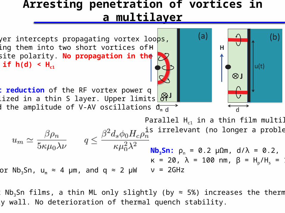
Arresting penetration of vortices in a multilayer
Parallel Hc1 in a thin film multilayer is irrelevant (no longer a problem)
I layer intercepts propagating vortex loops,turning them into two short vortices of opposite polarity. No propagation in the bulk if h(d) < Hc1
Great reduction of the RF vortex power q localized in a thin S layer. Upper limits of q and the amplitude of V-AV oscillations um
Nb3Sn: ρn = 0.2 μΩm, d/λ = 0.2, κ = 20, λ = 100 nm, β = Hp/Hs = 1/2, ν = 2GHzFor Nb3Sn, um ≈ 4 μm, and q ≈ 2 μW
Unlike thick Nb3Sn films, a thin ML only slightly (by ≈ 5%) increases the thermal impedance of the cavity wall. No deterioration of thermal quench stability.
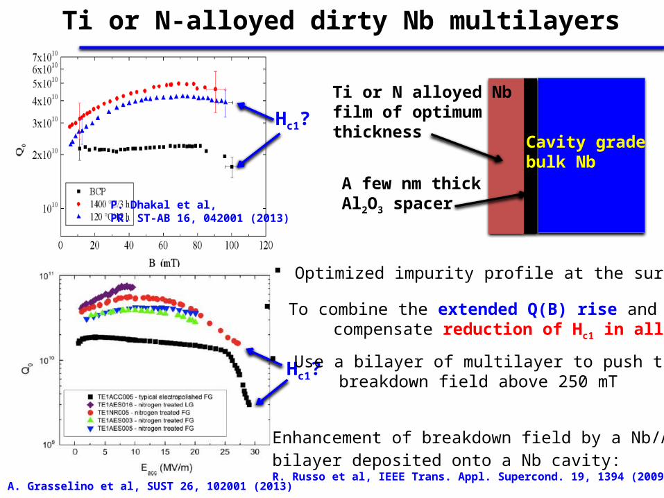
Ti or N-alloyed dirty Nb multilayers
A. Grasselino et al, SUST 26, 102001 (2013)
P. Dhakal et al, PR. ST-AB 16, 042001 (2013)
Hc1?
Hc1?Ti or N alloyed Nbfilm of optimum thickness
Cavity grade bulk Nb
A few nm thickAl2O3 spacer
Optimized impurity profile at the surface
To combine the extended Q(B) rise and compensate reduction of Hc1 in alloyed Nb
Use a bilayer of multilayer to push the breakdown field above 250 mT
Enhancement of breakdown field by a Nb/Al2O3 bilayer deposited onto a Nb cavity: R. Russo et al, IEEE Trans. Appl. Supercond. 19, 1394 (2009)

Conclusions
Multilayer S-I-S-I-S coating: breaking the Nb monopoly by taking advantage of superconductors with much higher Hc without the penalty of lower Hc1
Possibility to double the accelerating gradients and move from 2K to 4.2K
Optimum thickness at which the breakdown field is maximum
Multilayers with optimum thickness can reach breakdown fields exceeding the bulk superheating field of the layer material
Most promising ML materials: Nb3Sn, NbN and possibly pnictides
Dirty Nb multilayers could reach the breakdown field up to 30% higher than the superheating field of 200-240 mT for the cavity-grade Nb
New possibility of combination of the extended Q-rise in N or Ti-alloyed Nb and increased breakdown field