development of multifunctional software for evaluating the
TRANSCRIPT

Development of Multifunctional Software forEvaluating the Photonic Properties of New
Dielectric Composite Geometries
by
Daniel A. Cogswell
Submitted to the Department of Materials Science and Engineeringin partial fulfillment of the requirements for the degree of
Master of Science in Materials Science
at the
MASSACHUSETTS INSTITUTE OF TECHNOLOGY
June 2006
) Massachusetts Institute of Technology 2006. All rights reserved.
Author'. ... ... ............. .......Deparm'ent of Materials Science and Engineering
May 18, 2006
Certified b........................................................
W. Craig CarterThomas Lord Professor of Materials Science and Engineering
Thesis Supervisor
Accepted by.... .... ..... ....... ..............'"'>~~~t ~Samuel M. AllenPOSCO Professor of Physical Metallurgy
Chair, Departmental Committee on Graduate Students
ARCHIVES
MASSACHUSOF TEC
JUL
EiT'S INSrrTE,HNOLOGY
192006 1
-i--z-iLIBRARIES

2

Development of Multifunctional Software for Evaluating the
Photonic Properties of New Dielectric Composite
Geometries
by
Daniel A. Cogswell
Submitted to the Department of Materials Science and Engineeringon May 18, 2006, in partial fulfillment of the
requirements for the degree ofMaster of Science in Materials Science
AbstractSoftware was developed for solving Maxwell's equations using the finite-differencetime-domain method, and was used to study 2D and 3D dielectric composites. Thesoftware was written from the ground up to be fast, extensible, and generalized forsolving any finite difference problem. The code supports parallelization, allowing so-lutions to be obtained quickly using a beowulf cluster. An extension to the basicFDTD plane wave source was derived, allowing for the creation of angled, periodic,unidirectional plane waves on a square grid. 1D photonic crystal stacks were ar-ranged in a square array and it was discovered that sizeable bandgaps for 2D and3D geometries appear along the principle axes for different polarizations of the struc-ture. Furthermore, bandgaps in different directions and polarizations could be madeto overlap for reasonably large frequency ranges. The structure show promise foruse as a low-threshold lasing and may be optimized to produce a complete photonicbandgap.
Thesis Supervisor: W. Craig CarterTitle: Thomas Lord Associate Professor of Materials Science and Engineering
3

4
Acknowledgments
I would like to thank Craig Carter and Karlene Maskaly for guiding me through this
work. Craig has always provided sound advice, creative ideas, and encouragement,
and Karlene had to put up with many long phone calls and thoroughly answered
many long emails. The rest of the Carter Lab deserves credit for helping me stay
sane, especially when my software wasn't working or when I had to deal with crashing
computers. I thank my loving parents, sisters, and small group for encouragement,
support, and motivation, and for conversations on things other than research. I
particularly appreciated family vacations to Maine in the summer, and skiing with
my Dad in the winter. I also thank the members of the MIT Rowing Club, who
taught me that rowing a 2K on an erg is tougher than writing a masters thesis. And
lastly, I send appreciation to the Chicago White Sox and Boston Red Sox for their
World Series Championships that kept me in good spirits during tough times.
5

6

Contents
Contents 7
List of Figures 9
1 Introduction 13
1.1 Maxwell's Equations ........................... 13
1.1.1 Coulomb's Law ................... 1....... 14
1.1.2 Gauss's Law ................... 1......... 15
1.1.3 Ampere's Law . . . . . . . . . . . . . . . . . ........ 17
1.1.4 Faraday's Law . . . . . . . . . . . . . . . . . ........ 18
1.1.5 Maxwell's Equations ....................... 20
1.2 Constitutive Relations .......................... 21
1.3 Electromagnetic Plane Waves . ..................... 22
1.4 Electromagnetic Waves at an Interface . ................ 23
1.5 Wave Impedance ............................. 25
2 Photonic Crystals 27
2.1 The photonic bandgap .......................... 28
2.2 The quarter wavelength stack ...................... 29
2.3 Calculating photonic bandgaps ................... .. 29
3 The Finite-Difference Time Domain Approach 33
3.1 Finite Differences ............................. 33
3.2 TE and TM Modes ............................ 34
7

3.3 The Yee Algorithm .......................
3.4 Boundary Conditions.
3.5 Computational Setup.
3.6 Parallelization. .........................
3.7 Creating a source with the total/scattered field formulation .
3.8 An Angled Source .
3.9 Reflection Error.
4 2D Dielectric Structures
4.1 A new 2D structure .......................
4.2 2D Photonic Crystal Performance ...............
5 3D Dielectric Structures
5.1 A new 3D structure .......................
5.2 3D Photonic Crystal Performance ...............
6 Discussion
6.1 Discussion of results ....................
6.2 Discussion of software.
6.2.1 Philosophy on Reusable Software.
6.2.2 Implementation of Fourier Analysis ........
6.2.3 A Monte Carlo Method for Optimizing Bandgaps
6.2.4 Public software release ...............
6.3 The Future: Multi-physics Modeling ...........
A Reflectivity band diagrams for the 2D structure
B Reflectivity band diagrams for the 3D structure
References
8
35
36
37
38
41
43
46
47
47
50
53
53
55
59
. . . ... ... 59
. . . ... ... 60
. . . ... ... 60
. . . ... ... 61
. . . ... ... 62
. . . ... ... 63
. . . ... ... 63
65
73
77
List of Figures
1-1 An electromagnetic wave propagating in a vaccum. S is the Poynting
vector .................................... 23
1-2 Scattering of an electromagnetic wave at a dielectric interface. .... 25
2-1 Photonic crystals can be periodic in one, two, or three dimensions.
Colors represent materials with different dielectric constants[] ..... 28
3-1 There are two independent polarization modes, TE and TM, which
occur in 2D electromagnetic simulations ................. 34
3-2 The 3D Yee grid/2]. .............. ............... 35
3-3 The computational setup for calculating the reflectivity band diagram
of a dielectric structure. ......................... 39
3-4 An increase in performance is observed with a parallelized FDTD sim-
ulation. A point of diminishing returns is reached for a large number
of processors such that adding an additional processor does not signif-
icantly affect the running time of the simulation ............. 41
3-5 A Yee gridding of the electric and magnetic fields for a 2D TE mode
electromagnetic simulation. The total/scattered field formulation is
used to create a unidirectional, transparent source. .......... 43
3-6 Generation of a unidirectional angled plane wave with wavelength A
and angle S) ............. ................... . 45
9
4-1 The 2D structure that was investigated consists of periodically ar-
ranged quarter wavelength dielectric stacks. The bandgap was mea-
sured for two different orientations of the incident wave ......... 48
4-2 A comparison of the top and side TE bandgaps for the 1D array of
dielectric stacks with a coverage fraction of 30%. Significant overlap is
observed for TE mode, suggesting that the 2D structure may have a
full TE bandgap. ............................. 52
5-1 Views from different angles of the 3D dielectric structure that was
studied. The structure consists of rectangular-prism dielectric stacks
arranged in a square lattice. Characteristic lengths are labeled. d is
the width of a column, a is the thickness of a bi-layer, and a2 is the
lattice spacing of the columns ....................... 56
5-2 A comparison of the top and side bandgaps for the square array of di-
electric stacks for various coverage fractions. An overlapping bandgap
for all three modes is not quite opened, but the results suggest that
such an overlap may be possible. Gray boxes are used to illustrate
areas of high overlap ............................ 58
A-1 TE bandgap from the top direction of the 2D array of dielectric stacks
with n1 = 4.5 and n2 = 1.25 for various coverage fractions (d/a 2). . . 67
A-2 TM bandgap from the top direction of the 2D array of dielectric stacks
with n1 = 4.5 and n2 = 1.25 for various coverage fractions (d/a 2). . . 68
A-3 TE bandgap from the side direction of the 2D array of dielectric stacks
with nl = 4.5 and n2 = 1.25 for various coverage fractions (d/a2). .. 70
A-4 TM bandgap from the side direction of the 2D array of dielectric stacks
with n1 = 4.5 and n2 = 1.25 for various coverage fractions (d/a 2). .. 72
B-1 Bandgap from the top direction as a function of coverage for the square
array of 3D stacks with nl = 4.5 and n2 = 1.25. ............ 74
10

B-2 H polarized bandgap from the side direction as a function of coverage
for the square array of 3D stacks with nl = 4.5 and n2 = 1.25 ..... 75
B-3 E polarized bandgap from the side direction as a function of coverage
for the square array of 3D stacks with nl = 4.5 and n2 = 1.25 .... 76
11

12
Chapter 1
Introduction
"One scientific epoch ended and another began with James Clerk Maxwell."
-Albert Einstein
1.1 Maxwell's Equations
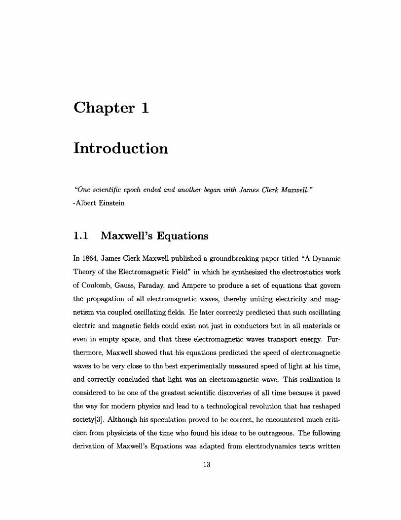
In 1864, James Clerk Maxwell published a groundbreaking paper titled "A Dynamic
Theory of the Electromagnetic Field" in which he synthesized the electrostatics work
of Coulomb, Gauss, Faraday, and Ampere to produce a set of equations that govern
the propagation of all electromagnetic waves, thereby uniting electricity and mag-
netism via coupled oscillating fields. He later correctly predicted that such oscillating
electric and magnetic fields could exist not just in conductors but in all materials or
even in empty space, and that these electromagnetic waves transport energy. Fur-
thermore, Maxwell showed that his equations predicted the speed of electromagnetic
waves to be very close to the best experimentally measured speed of light at his time,
and correctly concluded that light was an electromagnetic wave. This realization is
considered to be one of the greatest scientific discoveries of all time because it paved
the way for modern physics and lead to a technological revolution that has reshaped
society[3]. Although his speculation proved to be correct, he encountered much criti-
cism from physicists of the time who found his ideas to be outrageous. The following
derivation of Maxwell's Equations was adapted from electrodynamics texts written
13

by Jackson and Kong[4, 5].
1.1.1 Coulomb's Law
Charles-Augustin de Coulomb, in 1781, showed that he had produced a law which
describes the force of attraction between charged particles. His work has three impor-
tant consequences which nicely parallel Newton's equation of gravitational attraction.
Coulomb showed that the force between charged particles acted along a straight line
between the particles, varied as the magnitude of the charges and the inverse square
of the distance between the particles, and that the net force acting on a particle was
the vector sum of forces from all surrounding charged particles (i.e. a superposition
principle). Coulomb's Law is:kqiq2 ,F = r (1.1)
where F is the force vector, k is a constant and ql and q2 are the charges of the parti-
cles separated in space by a vector F. The hat notation (i.e. ) denotes a normalized
vector. The direction of the force is determined by the sign of the charges - like
charges repel and unlike charges attract. Interestingly, the definition of positive and
negative charge used today was chosen somewhat arbitrarily by Benjamin Franklin
who was fascinated with electricity and who first demonstrated charge conservation
experimentally[6].
Having obtained a force law for charged particles, it is useful to define the electric
field. It is appropriate to think of electrostatic attraction as occurring via a field
like gravity - each charged particle creates a field throughout all of space that other
particles feel and react to. The electric field created by a point charge q is defined as
the force acting on a unit charge that is placed at at distance from the point charge:
FE=- (1.2)q
The force term is defined by Coulomb's Law [Eq. 1.1], and thus the electric field
14
experienced by a unit charge (i.e. q2 = 1) due to the point charge q is:
E= r (1.3)
It is important to note that there is one small flaw with Coulomb's Law. It
assumes that there is instantaneous communication between the two point charges
that are interacting via electric fields, but Maxwell showed that the fields travel at
the speed of light. If the charges are travelling close to the speed of light, Einstein's
theory of relativity must be considered and we would have to turn to the field of
quantum electrodynamics.
1.1.2 Gauss's Law
Gauss's Law relates the electric flux through a closed surface to the charge enclosed
by the surface. Gauss's Law can be derived from Coulomb's Law by considering the
flux of the electric field, '1 E, through a closed surface. This flux is represented by a
surface integral:
b OE ^ ·iidA (1.4)
where dA is a small area patch on a closed Gaussian surface and h is the surface normal
of that patch. For any charges placed outside the surface, the net flux through the
surface will be zero because every imaginary field line that enters the surface will
eventually leave the surface. If the point charge q is contained within the surface,
field lines only pierce the surface once and the integral is not zero. If dA is projected
onto a sphere, the solid angle d subtended by the patch, located at a distance r
from the origin, is defined as the surface area of the patch when projected onto a unit
sphere with normal fi,:
dQR= ihdA (1.5)r2
If 9 is the angle between the surface normal of the patch and that of the sphere, that
is, the angle between h and ih, then t · dA = cosO dA and thus r2 dQf = cost dA.
15

Evaluating the surface integral [Eq. 1.4]:
E . hdA dA = kq d (1.6)
Because there are 4r steradians in a sphere:
JE · dA = 4kq (1.7)
which is Gauss's Law. The law reveals that the flux through any Gaussian surface
depends only on the amount of charge that lies within the surface. If the charge exists
in the form of a charge density p(F) rather than a collection of point charges, the law
can be written as:
JE * dA = 4rk p(F) dV (1.8)
Gauss's Law [Eq. 1.7] can be expressed in differential form by application of the
divergence theorem1 :
JsE .h dA = 4rk p()dV) V dV (1.lOa)
J (V . - 4rkp) dV = 0 (1.lOb)
Equation 1.10b can only be true if:
V E = 4rkp (1.11)
The issue of units in electromagnetism is complicated. Several systems are com-
monly used, and they each assign different units and magnitudes to the constants that
appear in electrostatics and electrodynamics equations. A good discussion of the dif-
ferent systems can be found in the appendix of Jackson's electrodynamics textbook.
1The divergence theorem describes a transformation between a surface integral and volume inte-gral for a vector field F [7]:
sF .fdA= JV. dV (1.9)
16
For the SI system, the constant k is defined as k = where EO is the permittivity
of free space. Gauss's Law then becomes:
V.E = (1.12)60
1.1.3 Ampere's Law
The relationship between magnetic flux density B and a steady state current I flowing
through a wire was measured by Ampere. He found the following inverse square
relationship which parallels Coulomb's law:
dB = kIdl x (1.13)
k is a constant 2 , and dl is a line element pointing in the direction of the current flow.
F is a vector from the line element to the point where the magnetic flux is to be
determined, and is a unit vector. The equation can be integrated to obtain:
B = |J x i 2 dV (1.14)
where J is the current density. This equation can be simplified3:
B =4 J x (- Fd V (1.16a)
B = V J v 1 dV (1.16b)
and because the divergence of a curl is zero:
V.B=O (1.17)
2For the SI units system, k = M0o47r
3The following equality is used for simplification:
2r =-V(ga~l ) (1.15)I j: (2 )
17

A relationship involving the curl of B can also be found from equation 1.16b:
Vx B = OV xV x j dV (1.18)47r i rl
Simplification of the above equation will not be presented. It is recommended that
the reader consult Jackson's electrodynamics text for a thorough treatment of the
solution[4]. Eq. 1.18 can be simplified to a simple relation which is Ampere's Law in
differential form:
V x B = of (1.19)
This relationship can be expressed in integral form with the application of Stokes
theorem 4:
j(V xBf) dA = uo dA (1.21a)
fB . d ipo jf- hdA (1.21b)
J · dl = i oI (1.21c)
Equation 1.21c expresses Ampere's discovery that looping magnetic flux is created
and is proportional to the electric current flowing through a loop.
1.1.4 Faraday's Law
All but Faraday's Law were derived from steady state observations. Faraday's time-
dependent observations were what later inspired Maxwell to realize that electric and
magnetic fields were closely related and lead to Maxwell's famous modification of
Ampere's Law. Faraday discovered that a changing magnetic flux induces a looping
electric current. He observed temporary variations in a steady-state current flowing
4 Stokes' theorem describes the equality of a line integral and a surface integral[7]:
s (Vx F) .fdA= J Fids (1.20)
S is a surface with normal A, C is a closed path on S with tangent t, and F is a vector field.
18
through a circuit as current in a nearby circuit was turned on or off, or if the second
circuit was moved relative to the first. He also observed temporary variations in
current if a permanent magnet was moved into or out of the circuit. His observations
can be expressed as:
=-k d (1.22)dt
where ~ is the electromotive force, k is a constant, and (IB is the magnetic flux through
a surface. The magnetic flux can be expressed as a surface integral of the magnetic
flux density B:
4T'B J B A . dA (1.23)
Furthermore, the electromotive force around the loop is the line integral of the
electric field:
&=j|E dl (1.24)
Equations 1.22, 1.23, and 1.24 are now combined:
dl = -k dtB (1.25)
/E d = -k d B * h dA (1.26)dt
If we assume E and B are in the same reference frame so that relativistic effects
can be ignored, Stokes's theorem can be applied to the left side of equation 1.26 to
obtain the differential form of Faraday's Law. The constant k disappears because it
is equal to unity in the SI system:
jtvxE) + idA = 0 (1.27a)
at (1.27b)V X 9+ 0O (1.27b)
19

1.1.5 Maxwell's Equations
A conservation law can be written for a flux of charge, since charge is a conserved
quantity:
T= -- J (1.28)
The equation states that the accumulation of charge p at a point is the negative
divergence of the electric current at the point - equivalent to the amount of charge
"arriving" at that point. Maxwell realized this and made a correction to Ampere's
Law, which had been derived for the steady state condition V J = 0. He used Gauss's
Law [Eq. 1.12] to evaluate and then substituted the result in the conservation law
[Eq. 1.28]. When simplified, the conservation law then becomes:
V.f+ -t=V (J+ =0 (1.29)
Maxwell called D the electric displacement field, and it represents the electric flux
density in a material 5 . Maxwell then replaced J in Ampere's Law (Eq. 1.19) with
the term J + 9, which he called the displacement current, and obtained an equation
that describes time-dependent fields:
ODV x H= J + at (1.30)
Having obtained a time evolution equation for the electric flux density, Maxwell
now had all the pieces necessary to describe electromagnetic waves. Maxwell's equa-
tions are:
VxE+ =0 (1.31a)at
V x H = J + at (1.31b)
V.D) =p (1.31c)
V*B =0 (1.31d)5see section 1.2 for a description of the relationship between D and E.
20
1.2 Constitutive Relations
Constitutive laws relate the electric field to the electric flux and the magnetic field
to the magnetic flux in a material. For linear, isotropic, nondispersive materials the
following relationships apply:
D = cE (1.32a)
B = pH (1.32b)
where e is the electrical permittivity tensor of the material and p the magnetic per-
meability tensor. Because only isotropic materials were simulated, scalars were used
for and Mi. To eliminate units, both properties are are generally referenced to their
values in a vaccum, Eo and Ao:
e = re0 (1.33a)
= r/o0 (1.33b)
Er is the relative permittivity and Ar is the relative permeability. Both are dimension-
less scalars, and r is commonly called the dielectric constant. o is the permittivity
of free space and /O is the permeability of free space. These variables are universal
physical constants with values of Co = 8.854 x 10⁻¹² farads/meter and o = 4r x 107
henrys/meter in SI units.
When studying dielectric composites, the index of refraction, n, is often reported
instead of the dielectric constant r. The index of refraction represents the ratio of
the speed of the electromagnetic wave in a vacuum (i.e. the speed of light) to the
speed in the material. The relationship between index of refraction and dielectric
constant is:
n = v/~d;7 (1.34)
Because the magnetic permeability was held constant for the analysis below, the
relative permeability Pr is unity, and the index of refraction only depends on the
21

dielectric constant:
n = J~ (1.35)
1.3 Electromagnetic Plane Waves
The solutions to Maxwell's equations give many important insights into the behavior
of electromagnetic waves in matter. To begin with, the equations have a travelling
plane wave solution6 of the form ei(k' -Zt). The existence of a travelling plane wave
solution explains why electromagnetic waves such as radio waves, infrared, light,
ultraviolet rays, and x-rays exist and are able to transport energy through space.
Maxwell realized that electric and magnetic fields hold potential energy much like
mechanical springs and that the oscillations of the fields allowed them to travel and
transport energy.
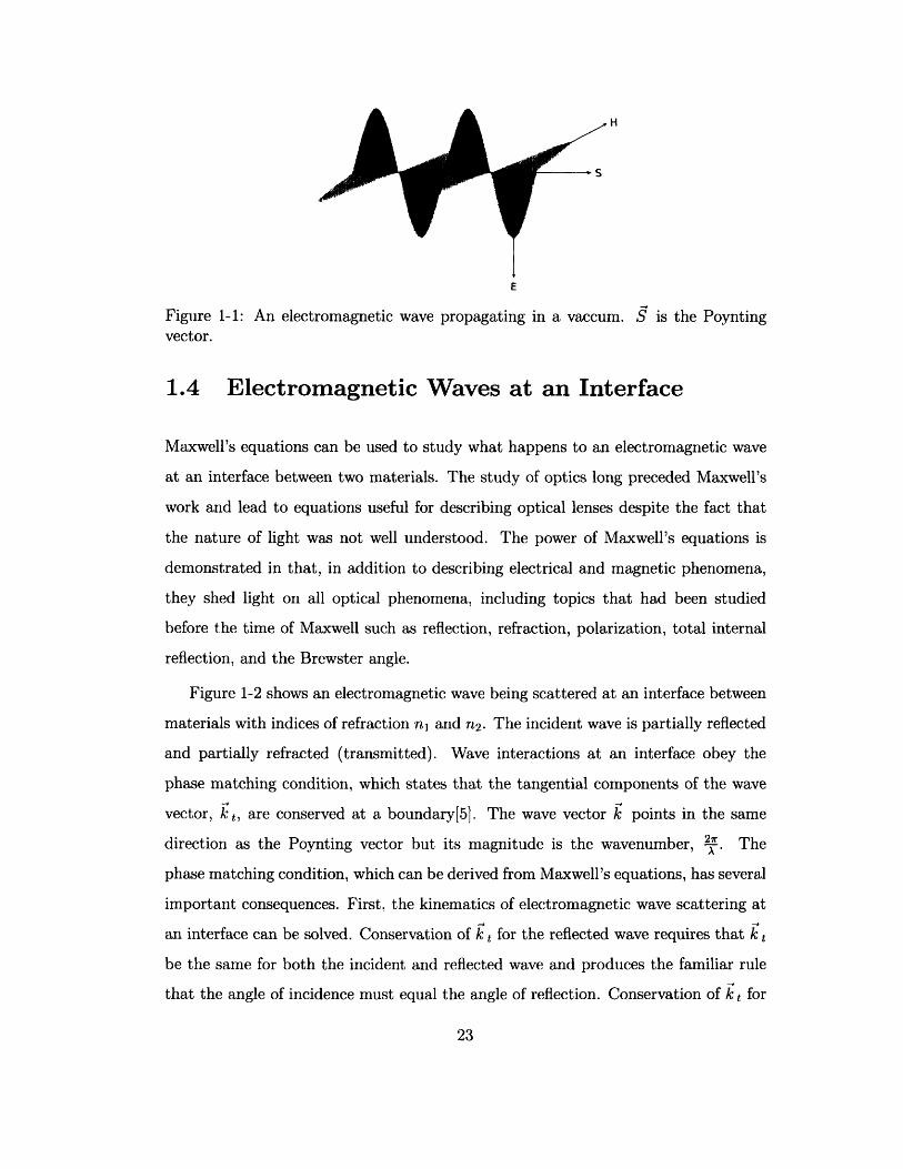
Figure 1-1 shows the magnitudes of the electric and magnetic field for an electro-
magnetic wave propagating in a vaccum. The wave propagates in the direction of the
Poynting vector S:
S=E x H (1.36)
The Poynting vector defines the direction of energy flow, and its magnitude expresses
the energy flux rate, or intensity of the wave (expressed in units of a"gy e) The
magnitude of the Poynting vector is used in Section 3.5 to measure the reflectivity of
dielectric structures. Because the magnitude of the instantaneous Poynting vector is
time-dependent (c.f. how the fields oscillate in figure 1-1), it is often useful to report
the time-averaged Poynting vector. The Poynting vector also plays a crucial role in
Poynting's theorems of energy and momentum conservation for electromagnetic fields
and systems of charged particles.
6A thorough proof is presented by Jackson[4].
22
I-, H
E
Figure 1-1: An electromagnetic wave propagating in a vaccum. S is the Poyntingvector.
1.4 Electromagnetic Waves at an Interface
Maxwell's equations can be used to study what happens to an electromagnetic wave
at an interface between two materials. The study of optics long preceded Maxwell's
work and lead to equations useful for describing optical lenses despite the fact that
the nature of light was not well understood. The power of Maxwell's equations is
demonstrated in that, in addition to describing electrical and magnetic phenomena,
they shed light on all optical phenomena, including topics that had been studied
before the time of Maxwell such as reflection, refraction, polarization, total internal
reflection, and the Brewster angle.
Figure 1-2 shows an electromagnetic wave being scattered at an interface between
materials with indices of refraction nl and n2. The incident wave is partially reflected
and partially refracted (transmitted). Wave interactions at an interface obey the
phase matching condition, which states that the tangential components of the wave
vector, kt, are conserved at a boundary[5]. The wave vector k points in the same
direction as the Poynting vector but its magnitude is the wavenumber, 2. The
phase matching condition, which can be derived from Maxwell's equations, has several
important consequences. First, the kinematics of electromagnetic wave scattering at
an interface can be solved. Conservation of k t for the reflected wave requires that k t
be the same for both the incident and reflected wave and produces the familiar rule
that the angle of incidence must equal the angle of reflection. Conservation of k t for
23

the refracted wave yields Snell's Law:
nlsin(01) = n2sin(02 ) (1.37)
When a wave propagates from a high refractive index material to a low refractive
index material, there will be a critical angle 0c such that when 0c is exceeded, the
tangential component of the incident wave vector k nlC becomes larger than the total
wave vector k in the material with index n2. Thus t cannot be conserved at the
interface for a transmitted wave and the result is total internal reflection. 0c can be
found by solving Snell's Law [Eq. 1.37] with 02 = 90°:
0 = sin- I n2 (1.38)
Another interesting phenomenon occurs when k trans = k nc, where kn is the value
of the normal component of the wave vector. This condition corresponds to k n being
conserved across the interface. In this case, the Fresnel equations [Eq. 1.41] reveal
that there is no reflected wave; all waves are transmitted. The angle at which this
occurs is b, the Brewster angle, which can be found by solving the Fresnel equations
for zero reflectivity and employing Snell's Law. Interestingly, the Brewster angle only
exists for TM polarized waves (TM is defined in Section 3.2):
Ob = tan- I G' = tan-l £ (1.39)_inc1 =
The amount of light that is reflected and refracted when a wave scatters at an
interface can be calculated from the Fresnel equations. F is the reflection coefficient,
the ratio of reflected power to incident power, and r is the transmission coefficient,
the ratio of transmitted power to incident power. and r are related for a lossless
material such that:
+T = 1 (1.40)
The values of the reflection coefficient depend on the polarization of the incident
24
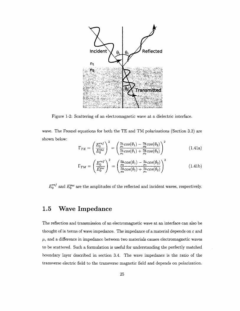
Figure 1-2: Scattering of an electromagnetic wave at a dielectric interface.
wave. The Fresnel equations for both the TE and TM polarizations (Section 3.2) are
shown below:
NEref 2rTE =E: n
Eon
tEref 2
rTM - E77wnc )FTM = 0neEf
( CScos(O1) _ 2cos(2) _ l A2
I ilcos(Ol) + 2 cos(o2)
_ COS(1) - l COS(2) 2
2coS(01) + ' Cos(02)
(1.41a)
(1.41b)
E ~f1 and E' nC are the amplitudes of the reflected and incident waves, respectively.
1.5 Wave Impedance
The reflection and transmission of an electromagnetic wave at an interface can also be
thought of in terms of wave impedance. The impedance of a material depends on E and
/A, and a difference in impedance between two materials causes electromagnetic waves
to be scattered. Such a formulation is useful for understanding the perfectly matched
boundary layer described in section 3.4. The wave impedance is the ratio of the
transverse electric field to the transverse magnetic field and depends on polarization.
25

Wave impedance is given as[4]:
ZTM = cos()1 - (1.42a)
ZTE = -i= a1 (1.42b)we cos(O) E
k n is the normal component of the incident wave vector and w is the angular frequency.
For normal angles of incidence, the impedance can be simplified to Z = VI and for
angles larger than Oc, the impedance is imaginary[5]. The reflection and transmission
coefficients are defined, in terms of the impedance in materials nl and n2 from figure
1-2, as:
Z1 - (1.43a)Z + Z2
2Z2r- 2 1 (1.43b)Z2 + I
26

Chapter 2
Photonic Crystals
Photonic crystals are periodic arrangements of materials with different dielectric con-
stants that affect the behavior of light. The crystal's geometry exploits the simple
reflection and transmission rules for electromagnetic waves as discussed in section 1.4
in such a way that new and useful optical behaviors are produced. Photonic crys-
tals can be used to create perfect dielectric mirrors, light filters and sensors, efficient
lasers[8], and waveguides for light. Defects in photonic crystals can be used to trap
and control single photons of light[9]. Photonic crystal structures are being used
in the development of optical circuits[10], and there has been recent interest in the
phenomenon of negative refraction that can be produced with photonic crystals[11].
The study of photonic crystals does not involve more sophisticated concepts than
were developed by Maxwell and others in the 1800's. Although Maxwell could have
envisioned photonic crystals, they have only recently been studied seriously because
advances in manufacturing techniques have allowed the design of structures on the
nanoscale.
Because the wavelength of visible light is about 400nm to 700nm, the structures
that create novel behavior must be of roughly the same dimensions. An interesting
feature of Maxwell's equations is that they are scalable such that the solution is inde-
pendent of length scale. Thus a solution at one length scale can be scaled and apply to
the same system at any other length scale. Thus when simulating a photonic crystal,
the geometry should be considered rather than the absolute size of the structure.
27

Figure 2-1: Photonic crystals can be periodic in one, two, or three dimensions. Colorsrepresent materials with different dielectric constants[1].
2.1 The photonic bandgap
Photonic crystal geometries are categorized by their periodicity. Figure 2-1 shows how
materials with different dielectric constants may be combined to produce geometries
that are periodic in one, two, and three dimensions. The periodicity of the crystal is
an important factor that controls the crystal's photonic properties[12].
One of the most important features of photonic crystals is that they may have
photonic bandgaps. The photonic bandgap is analogous to electronic bandgaps in
semiconductors, except that the electrons from solid-state electronics are replaced by
photons. A photonic bandgap can be thought of in a couple of ways. A material with
a photonic bandgap will reflect all light over a frequency range and transmit none of
it, the density of photonic states within the crystal goes to zero in the bandgap, and
the modes within the band gap are evanescent (exponentially decaying).
If a photonic crystal reflects light of any polarization incident at any angle, then
it has a complete photonic bandgap. 1D and 2D dielectric structures may have a
bandgap in one and two directions respectively, but they will not have a complete 3D
bandgap because there is no periodicity to scatter electromagnetic waves in at least
one direction. 3D photonic crystals are candidates for complete photonic bandgaps,
but because they are much harder to manufacture than their D or 2D counterparts,
they should only be used for applications where a complete bandgap is required. Many
dielectric geometries in 1D, 2D, and 3D have been shown to have complete bandgaps
for their respective dimensions. Furthermore, many of these structures have been
28
fabricated and the bandgap confirmed experimentally. Commonly studied photonic
crystal geometries include the quarter-wavelength stack in D, arrays of dielectric
circles, circular voids, or linear veins in 2D, and, in 3D, lattices of voids or dielectric
spheres[12]. Other more complex 3D geometries have been discovered[1, 13], including
some bi-continuous, triply periodic minimal surfaces that can be manufactured by
interference lithography.
2.2 The quarter wavelength stack
The D photonic stack is a simple structure that exhibits a bandgap and that will
be used as the basis for development of more sophisticated 2D and 3D structures in
chapters 4 and 5. If the layers of a D photonic crystal (leftmost image, figure 2-1)
are chosen such that light of wavelength A travels a distance A/4 in each layer, the
structure will have a bandgap at normal angles of incidence and is called a quarter
wavelength stack. The bandgap exists because all of the light that is reflected at the
boundaries constructively interferes and emerges from the structure perfectly in phase.
Consider the phase of a plane wave as it penetrates the structure and is partially
reflected at each interface. The light that emerges from the quarter wavelength stack
has travelled an integer multiple of A/2 in each layer, because it must pass through
the layer completely at least twice - once when incident and once when reflected.
Additionally when light is travelling in a material with low dielectric constant and is
reflected by a material with higher dielectric constant there is a phase change of ir.
The combined effect of these observations is that all of the light is eventually reflected
and exits the structure in phase, producing a bandgap.
2.3 Calculating photonic bandgaps
The calculation of a photonic bandgap requires solving Maxwell's equations for a
dielectric structure. Frequency domain and time domain algorithms are two different
approaches are commonly used to solve Maxwell's equations, and each method has
29

advantages and disadvantages.
The frequency domain approach involves solving Maxwell's equations for eigenval-
ues and eigenfunctions, analogous to computing the Bloch wave function in quantum
mechanics. It is frequency domain because it determines the wave mode eigenfunc-
tion H (r) for a specific frequency w that is directly related to the eigenvalue (w/c)2.
Maxwell's equations are decoupled to produce a Schrodinger-like equation that can
be solved for eigenfunctions and eigenvalues[12]:
x ( x H(r) = (r) (2.1)
The frequency domain is appropriate for determining dispersion relations for photonic
crystals and for analysis of the photonic band structure, which describes how the
wavelength of a propagating wave varies with frequency.
The time domain solution is obtained by iterating Maxwell's equations through
time on a spatial grid. The state of the system is known at a specific time, but not
necessarily for any specific frequency. Time domain simulations allow for analysis of
where fields concentrate in the system and are useful for measuring transmittance
and decay times. Time domain simulations, unlike frequency domain simulations,
are not restricted to solving for periodic structures because of the development of
absorbing boundaries that effectively create a computational domain extending to
infinity. Thus any arbitrary, finite system can be simulated. Unfortunately, unlike
frequency domain simulations, time domain simulations do not scale well with changes
in grid resolution or system size. Also, in the time domain, closely spaced modes
may not be distinguishable if the frequency resolution is not high enough. Such a
resolution problem will not happen in the frequency domain because different bands
are represented by different eigenvalues.
An advantage of the time domain is the ability to solve for a system's response
to all frequencies from just one simulation. In the frequency domain for comparison,
a new simulation must be run for each frequency to be investigated. This ability
is possible in the time domain because the time domain and frequency domain are
30

related via Fourier transforms. A measurement of the response over all frequencies
can be achieved by measuring the system's response to an impuse function, which
contains all frequencies. As described by Weaver [14], the function y(x) that describes
the response of the system to an input function f(x) is given by the convolution of
f(x) with h(x), the response of the system to the impulse function:
y(x) = f(C)h(x - ) <d (2.2)
31

32

Chapter 3
The Finite-Difference Time
Domain Approach
3.1 Finite Differences
FDTD simulations use the method of centered finite differences to solve differential
equations numerically on a grid. At a point i,j,k in space, the derivatives in the
x-direction are approximated from the values at neighboring points using centered
differencing:u _ Ui+l,j,k - Ui-lj,k + [(AX) 2] (3.la)
,Ox 2Ax
02U Ui+lj,k - 2Uij,k + Ui.l,j,k
Ox2 (AX) 2
where Ax is the distance between gridpoints in the x-direction. Equations for deriva-
tives in other directions have the same form. This method is "centered" because one
point on either side of Ui,j,k is used to compute the derivative. The method is only an
approximation of the actual derivative, because the derivative is defined in the limit
that the grid spacing goes to zero. The amount of error for centered differencing is
proportional to (Ax)2, and thus it is second-order accurate. Although the differenc-
ing scheme has been presented for spatial derivatives, it will also be used to compute
temporal derivatives and will provide second-order accuracy in time.
33

Transverse Magnetic Mode (TM)
(a) (b)
Figure 3-1: There are two independent polarization modes, TE and TM, which occurin 2D electromagnetic simulations.
3.2 TE and TM Modes
Three vectors are needed to find a solution to Maxwell's curl equations because the
cross product in the equations relates three orthogonal vectors. For simulation of a
2D structure there are two possible polarizations to choose from when assigning fields
to the 2D computational grid. These two modes are illustrated in figure 3-1, where it
can be seen that either H., Hy, and Ez or E, Ey, and H must be chosen as the fields
to simulate. The modes are called transverse electric (TE) and transverse magnetic
(TM) respectively. Interestingly, it can be derived from Maxwell's equations that
the two modes are uncoupled and will not always produce the same behavior. There
is disagreement on the naming of the different modes. Joannopoulos, for instance,
defines the two modes exactly opposite to the definition used in this work[12].
In terms of the Poynting vector, the two modes represent the only two possible
polarizations for a 2D plane wave. Recall that the Poynting vector S is the cross
product of the E and H fields. The Poynting vector can be rotated about its axis
such that its direction and magnitude remain constant but E and H are rotated in
the plane normal to S. The different orientations of E and H represent different
polarizations. Polarizations in 3D do not fit into these two categories, and the possible
polarizations are related to the point group symmetry of the structure.
34
2D Computational Domain 2D Computational Domain
Transverse Electric Mode (TE)
Ez H, Hz E,

z
(ij
Figure 3-2: The 3D Yee grid[2].
3.3 The Yee Algorithm
In 1966, Kane Yee developed a simple, efficient, and powerful algorithm for numer-
ically solving Maxwell's equations on a finite grid[15]. His algorithm is still widely
used today. Yee used a centered differencing scheme [Eq. 3.1a] to solve Maxwell's
equations [Eq. 1.31] for both the electric and magnetic fields in space and time. Mod-
eling both fields produces robust solutions and allows for the modeling of electric and
magnetic material phenomenon.
A Yee grid for a two dimensional TE mode simulation is illustrated in figure 3-5,
and a 3D gridding is shown in figure 3-2. In the Yee grid, the magnetic and electric
fields are offset from each other by 1 of a gridpoint. This allows Yee's gridding scheme
to implicitly solve Gauss' divergence laws [Eq. 1.31c, 1.31d] because each E field point
is surrounded by a loop of H field points, and each E field point is surrounded by a
loop of H field points. Thus the scheme naturally captures the ideas of Ampere's and
Faraday's Laws where flux of an electric or magnetic field through a point induces a
loop of either electric or magnetic field, and evolution of Maxwell's equations through
time is achieved by employing only the time-dependent curl equations [Eq. 1.31c,
1.31d].
35
The Yee algorithm uses a leapfrog timestepping approach, where each timestep is
divided into two parts. In the first half of the timestep the electric field is updated.
In the second half, the magnetic field is calculated using the just updated electric
field values. This approach is explicit and second-order accurate in time because it
is centered in time. Were forward or backward time differencing used, the solution
would only be first-order accurate in time. The Yee discretization of Maxwell's curl
equations [Eq. 1.31a, 1.31b] is shown below for the x direction:
D (i + 1, )-Dz 2(i + 2, , k) Hn(i + j + k) -Hn(i + 1, -At Ay
Hy(i + 1, j, k + Hy(i + 1, j, kAz
B~n+1 +(i, j+ i E (iJ+ + 1) , k)At Az
E+ (i, j + 1, k + ) - E+ 2(i,j,k + 2)Ay
The equations for the y and z directions are similar in form. The 2D equations for
both the TE and TM mode can be found by eliminating the k index and setting
the appropriate fields equal to zero. For TE mode Ex = Ey = 0, and for TM mode
H = H = 0.
3.4 Boundary Conditions
An absorbing boundary called a perfectly matched layer, or PML, was used in the
simulations presented below. This particular boundary condition was developed by
Berenger[16]. The PML allows for simulation of an infinite computational domain
by attenuating the electromagnetic waves at the boundary with minimal reflection.
Terminating the computational domain or introducing an artificial boundary causes
the electromagnetic waves to be reflected back into the simulation and inhibited
36

the initial use of FDTD for electromagnetic simulations. Several other absorbing
boundary algorithms have been proposed, but Berenger's method remains one of the
most accurate, and also damps waves at angles of incidence other than the normal
angle.
Berenger's PML exploits the fact that if and are chosen in two different
materials such that the impedance Z (as described in section 1.3) in each material is
the same, there will not be any reflection at the interface. Furthermore, the waves
can be made to decay with the use of complex values for p and e. Berenger's method
also involves a field-splitting modification of Maxwell's equations for the gridpoints
in the PML boundary layer that is necessary to decay the waves. An implementation
of the PML coded by Sullivan was incorporated into the developed code[17].
3.5 Computational Setup
The grid layout used to calculate reflectivity band diagrams of dielectric compos-
ites using the finite difference method is illustrated in figure 3-3. A unidirectional
plane wave is generated from a line source, and allowed to propagate through a vac-
cum toward a dielectric structure. The plane wave then interacts with the dielectric
structure and is partially reflected and partially transmitted. The amplitude of the
reflected and transmitted waves changes, but their frequencies do not. The reflected
and transmitted waves are measured at the indicated locations in figure 3-3 after the
system has reached steady state. The reflected signal must be measured behind the
unidirectional source where only the scattered field exists; both the incident and re-
flected waves exist in the region between the source and the structure. Measurement
of the reflected or transmitted wave involves computing the time-averaged power over
a region of gridpoints. The power of an electromagnetic wave is the magnitude of
the Poynting vector, E , averaged over time. The reflectivity is the ratio of aver-
age reflected power to average incident power, which is the same as the ratio of the
37

time-averaged Poynting vectors. Reflectivity can be expressed as:
r = _ 2 (33)
where E r is the electric field of the reflected wave and Ei that of the incident wave.
nr and ni are the number of gridpoints over which 1E is summed in the reflected
and incident regions respectively (i.e. spatial averaging). The angled brackets denote
time averaging. It should be noted that because = for electromagnetic
waves, the reflectivity could also be measured in a similar manner using the magnetic
field.
The length of time for which the reflected power is averaged must be constrained
to correspond to the passage of an integer number of wavelengths. In this study, 24
periods was found to be sufficient to produce stable results, and transmitted power r
was measured instead of reflected power. r was found from the relationship F -r = 1,
which holds for the perfect dielectrics (i.e. a = 0) that were simulated. Measuring the
transmitted power produced bandgaps that accurately matched accepted results[18]
and transmitted power was measured when calculating the bandgaps in the appen-
dices. Measuring reflected power directly produced results that occasionally deviated
slightly from the accepted results. The error was not large, and it is possible that
there was an interaction between the reflected waves and the unidirectional source.
Although it is supposed to be transparent, the unidirectional source may have slightly
interacted with reflected waves.
3.6 Parallelization
The software developed was designed to support massive parallelization. The FDTD
approach is easily parallelized for solving general finite difference problems across
multiple CPUs. FDTD simulations were parallelized using a divide and conquer
approach illustrated in figure 3-4a. This approach is well suited for FDTD because
38

Absdrbing Boundary"
Dielectric StructureI II I
I II I~~I Me~~~I~u m | Moncilron trncmicinn I
- Absorbing oundary
…----- --- Periodic Boundary
Figure 3-3: The computational setup for calc(ulating the reflectivity band diagram ofa dielectric structure.
the central differencing scheme used requires only that the immediate neighbors of a
gridpoint be known in order to advance that gridpoint in time. Thus the large grid
illustrated in figure 3-3 can be divided into many smaller subgrids illustrated in figure
3-4a, which can be evaluated in parallel by separate processors.
When the original grid is divided into subgrids, each gridpoint at the boundary
of two subgrids will be missing neighbor that it needs and which is stored on
an adjacent subgrid, possibly located in the nemory of a different CPU. Thus to
insure that every gridpoint can be evallated, each subgrid must exchange boundary
gridpoints with its neighboring subgrids at the end of each timestep. Exchange of
boundary layers is illustrated with arrows in figure 3-4a. The exchange of boundaries
must be completed at the end of each timrestep and before the next tirnestep can be
evaluated.
The division of the original large grid ito several smaller grids for parallelization
was designed to be as transparent ats possible for future progralmers. Parallelization
39
I · _~~~~~~~~~~~~~~~~~~~~~~~~~~~~I
Al
I

is implemented for an arbitrary number of processors provided by the user at runtime,
and the user does not have to worry about how to divide and distribute the work -
the division is performed automatically. The software contains logic for choosing how
to divide up the initial large grid into smaller subgrids. The software analyzes the
dimensions of the grid to compute which direction to divide it. It is advantageous
to divide the grid in such a way as to minimize the size of the boundaries between
subgrids because these boundary values will be exchanged, possibly over an ethernet
connection which may cause a bottleneck. Each subgrid is a C++ object that keeps
track of its neighboring subgrids and therefore knows its absolute position in the
overall grid. Items that the programmer places in the grid, such as dielectric struc-
tures, plane-wave sources, or measuring points can then be referenced using absolute
coordinates and not the relative coordinates for the specific subgrid that the objects
exist in. Additionally, objects can span multiple subgrids without needing special
attention.
Parallelization was implemented using the Message Passing Interface (MPI) which
is a standard language for writing parallel and distributed programs. Because MPI
is a communication protocol rather than an implementation, it does not require any
specific hardware, operating system, or compiler and works efficiently for many com-
puter configurations. CPUs used for parallel computation can be virtual, located
on a multi-processor system using shared memory, or located on computers that are
networked together.
Parallelization provides two important advantages for electromagnetic FDTD sim-
ulations. First, it provides a measurable speed increase. Figure 3-4b shows that the
running time of a 2D FDTD simulation is improved as more CPUs are added. The
second advantage of parallelizing FDTD simulations is that it eliminates a potential
memory bottleneck. With a single processor simulation, the size of the simulated
system is limited by the size of a grid that can fit in the computer's memory without
causing a memory overflow. The maximum size of a parallel grid is related to the
sum of the memory in every computer being used to solve the problem. If the system
becomes too big for one node in the cluster, adding more computers will make the
40

Dielectric Structure
Effect of Parallelizing a 2D FDTD Simulation of 450,000 Gridpoints
CPU
350
300
u 250
CPU 2 - 200
a: 150
100
50
CPU 3
[ '&. A'barbing~Bnd&r"':¥-I Number of processes
(a) (b)
Figure 3-4: An increase in performance is observed with a parallelized FDTD simula-tion. A point of diminishing returns is reached for a large number of processors suchthat adding an additional processor does not significantly affect the running time ofthe simulation.
problem solvable. In this way it's possible to solve problems on a cluster of computers
that are much too large to solve on any one computer in the cluster alone. Addition-
ally, 32-bit memory addressilng limits the size of a grid on a single CPU to 4Gb. With
this parallelization scheme, the 4Gb limit is avoided on 32-bit machines because the
parallelization scheme effectively implements a distributed memory architecture.
3.7 Creating a source with the total/scattered field
formulation
A efficient unidirectional, periodic, angled source was derived for use in FDTD electro-
magnetic simulations. The source was developed by modifying the total-field/scattered-
field boundary as described by Taflove and HagIless[2]. This approach is based on the
idea that for an electromagnetic plane wave interacting with a dielectric, the total
41
V• '1: ts~~~~~~s:6~_
Measure reflectance
Plane-wave source
A .' ~' mr---- wm __-m.___
Measure transmissionMeasure transmission
I,"E
[ i I , I
...... '1.AA - ~ ~~~I I . 1
I\
_ __ __ __ __ __ _ _ __ __ __ __ __
-----------------------
I
. " " '"Y " "'

wave is the sum of the incident and scattered parts:
E total = E inc + E scat (3.4a)
H total = H inc + H scat (3.4b)
In general, an FDTD electromagnetic simulation will evolve the total field, al-
though it is often the scattered field that is desired for analysis. The incident field is
known because it is defined by the programmer as some time-varying field: often a
plane wave or Gaussian pulse. The scattered field can only be found by subtracting
the incident field from the total field. The simplest way to calculate the scattered
field is to run two simulations. One simulation contains the dielectric structure and
is used to calculate the total field. The second simulation simulates the incident
field on a grid of identical dimensions, but with the dielectric structure replaced by
vacuum (n = 1.0). The scattered field is found at each timestep by subtracting the
incident field from the total field. Although this approach is conceptually simple, it
is inefficient. Twice the number of gridpoints and memory are required, resulting in
the simulation being slow and possibly causing a memory overflow. If the simulation
is run in parallel, twice as many boundary values must be passed between subgrids.
The total/scattered field boundary formulation provides an efficient way of sepa-
rating the scattered field from the total field and allows for the introduction of non-
physical unidirectional transparent sources. A unidirectional source is non-physical
because any line or plane of oscillating fields in a physical system will produce a wave
that propagates away from the source in all directions. Unidirectionality is effectively
achieved by cancelling out the propagation of the wave in one direction, creating a
total/scattered field boundary.
Figure 3-5 illustrates the formulation of the total/scattered field for TE polariza-
tion. A similar figure applies to the formulation for TM. The formulation corrects
inconsistencies that develop at the boundary between a total and scattered field. Such
a boundary is illustrated with white and shaded regions in figure 3-5. The boundary
is located between gridpoints jb and jb + 1/2. Application of the Yee equations re-
42
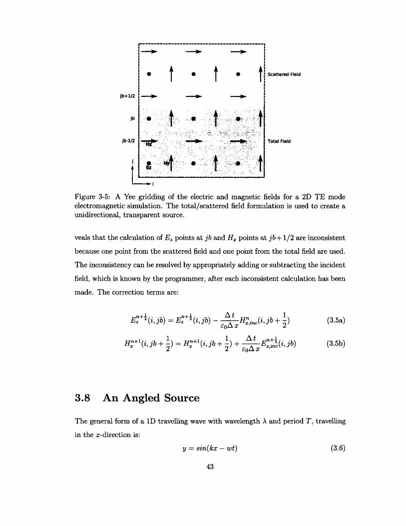
jb+1/2
jb
Jb-1/2
A A_ _ AScattered Field
Total Field
I
Figure 3-5: A Yee gridding of the electric and magnetic fields for a 2D TE modeelectromagnetic simulation. The total/scattered field formulation is used to create aunidirectional, transparent source.
veals that the calculation of Ez points at jb and Hz points at jb+ 1/2 are inconsistent
because one point from the scattered field and one point from the total field are used.
The inconsistency can be resolved by appropriately adding or subtracting the incident
field, which is known by the programmer, after each inconsistent calculation has been
made. The correction terms are:
Ezn+(i,jb) = En+2(i,jb)- --- Hin(ijb+-) (3.5a)
1 1 A t n+,H'+l(i, jb+ ) = Hn 1+l(i, jb ) + E (i, jb) (3.5b)
2 2 eA x , ' zinc,
3.8 An Angled Source
The general form of a 1D travelling wave with wavelength A and period T, travelling
in the x-direction is:
y = sin(kx - wt) (3.6)
43
, .· I * ''
.. : : . < .. 2 .I ? . ~ ::::~:t~::,,:: :,:, i, tH a 'I' ' ': ': : : ' ' : ', :,. ,,
zt : . : , : : * i $ e ?,,L · ': ·· ,·1. ·:·. I:* ·n~..: · ··_ _
-------------------------------------------

where k = 2 is the angular wavenumber, x is the position, w = 2 is the angular
frequency, and t is time. As time progresses, the amplitude at each x position changes
and the wave is observed to propagate. In the case of electromagnetic waves propa-
gating through a vacuum, the velocity at which the wave propagates is the speed of
light, c.
In 2D and 3D FDTD electromagnetic simulations, a periodic plane wave can
be generated from a line or plane of discrete gridpoints that oscillate in phase, as
illustrated in figure 3-3. A line of oscillating fields in 2D and a plane in 3D generate a
plane wave because, according to Huygens' principle, all points on a wavefront serve
as point sources of spherical secondary wavelets. After a time t, the new position
of the wavefront will be that of the surface tangent to these secondary wavelets[19].
Each point on the source line or plane contributes a spherical wavefront to the tangent
surface of a plane wave. However, creating an angled incident wave on a square FDTD
grid is troublesome. A simple solution would be to place the source line or plane at
an angle relative to the grid, but the plane wave source must be periodic so that it
is compatible with periodic boundaries. If the source is simply inclined relative to
the grid, the source is not periodic because the source is not continuous across the
periodic boundaries. The same periodicity argument can be made for keeping the
source fixed and simply rotating the dielectric structure - the rotated structure will
not be periodic. Placing the source at an angle relative to the grid introduces aliasing
as well because an angled line of points cannot be exactly represented on a square grid
- the sampling of points along the line will be non-uniform, and the nonuniformity
will depend on the angle of the source. Low inclination angles would be particularly
troublesome.
If the incident field varies periodically in time along the x-direction of the source
line, an angled plane wave will be generated. Because the systems being investigated
are periodic in the x-direction, the variation of the field in that direction must also
be periodic such that an integer number of wavelengths fits along the x-axis. The
consistency rule is:
mA = nx sin(O) (3.7)
44
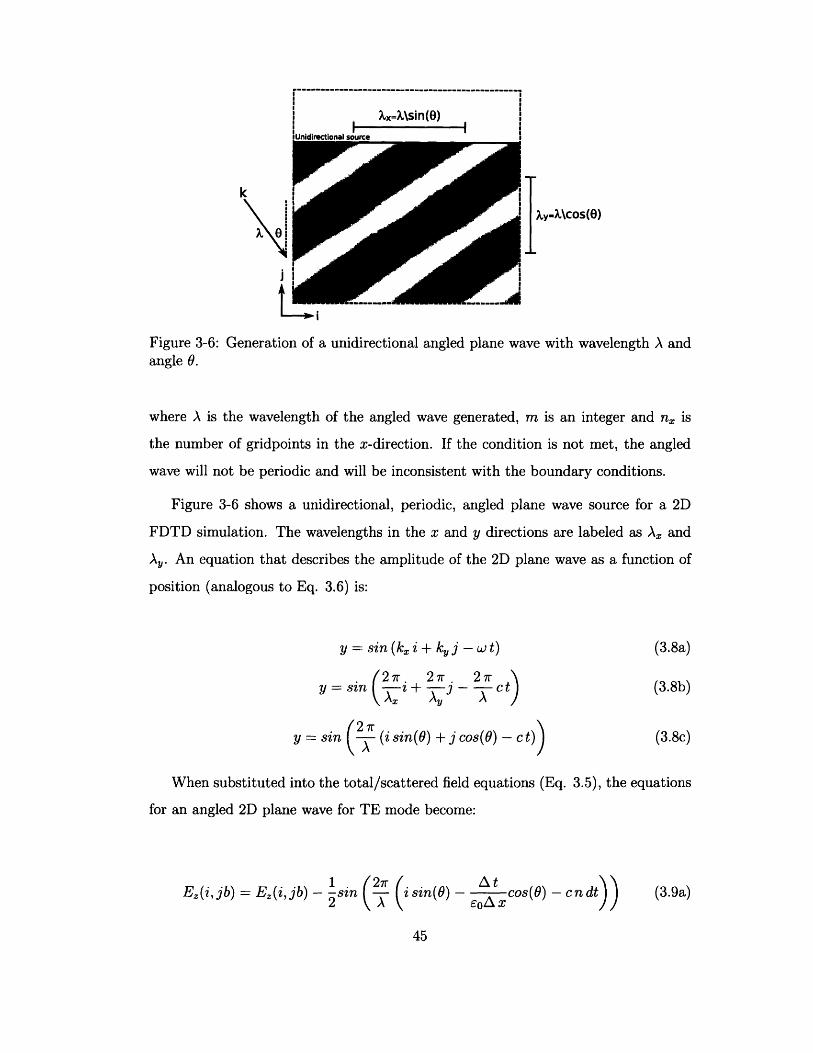
~~~~~~~~~I II IX=X\sin(e)I I* I I I
k
i
t
Figure 3-6: Generation of a unidirectional angled plane wave with wavelength A andangle 0.
where A is the wavelength of the angled wave generated, m is an integer and n is
the number of gridpoints in the x-direction. If the condition is not met, the angled
wave will not be periodic and will be inconsistent with the boundary conditions.
Figure 3-6 shows a unidirectional, periodic, angled plane wave source for a 2D
FDTD simulation. The wavelengths in the x and y directions are labeled as A, and
A. An equation that describes the amplitude of the 2D plane wave as a function of
position (analogous to Eq. 3.6) is:
y = sin (kx i + kj - wt) (3.8a)
= sin( i+ - ct) (3.8b)
y = sin (2 (i sin() + j cos() -c t)) (3.8c)
When substituted into the total/scattered field equations (Eq. 3.5), the equations
for an angled 2D plane wave for TE mode become:
1( ) = (2r ( - (td)) (3.9a)Ez,(i'.,jb)= E(i, jb) -s - i sin(O)C xOS(O) -cndt (3.9a)
2 A ~So'A
45
H.(i,jb+) =H (i, jb+)+ sin (isin(9) -c(n .5)dt) ( (3.9b)
The co() term in equation 3.9b projects the angled Hi,c onto the x-axis of the
grid's coordinate system. Similar arguments were used to derive angled sources for
TM mode and also in 3D.
3.9 Reflection Error
The PML described in section 3.4 is, unfortunately, not a completely perfect absorber
and this fact has important consequences for the periodic angled source. Because
the PML is terminated at the boundary of the simulation domain, there is a small
nonphysical reflection back into the simulation domain. This reflection error, R(O),
is found to be[2]:
R(O) = e- 2 q7dcosO (3.10)
where r and a are the characteristic wave impedance and conductivity of the PML.
Unfortunately for the angled periodic source, the reflection error increases with the
exponential of cos(O). This means that as the angle of incidence approaches 90°, the
PML becomes completely ineffective. The angle of incidence used in a simulation
should be kept as small as possible to minimize reflection error and the angled source
should be used cautiously. Reflection error should not prohibit the use of the angled
source because there will be very little error for small angles.
46

Chapter 4
2D Dielectric Structures
4.1 A new 2D structure
A quarter wavelength stack (section 2.2) was used as a starting point for developing
a new photonic crystal geometry that may possess desirable optical properties and
potentially a complete photonic bandgap. A drawing of a 2D version of the proposed
structure is shown in figure 4-1 (Chapter 5 deals with an analogous 3D structure).
The design consists of introducing periodic gaps in a D quarter wavelength stack, or
alternatively, placing rectangular quarter wavelength stacks on a D lattice. Figure 4-
1 also demonstrates the two configurations for which bandgap calculations were made.
Figure 4-1a shows the top configuration, and figure 4-lb shows the side configuration.
In both cases, the computational domain was periodic in the direction normal to the
incident wave vector. For the top direction, an infinite line of stacks with a finite
number of bi-layers was simulated, while for the side configuration a finite number of
stacks with an infinite number of bi-layers was simulated.
In all 2D calculations of the top configuration, 4 bi-layers were used for each
dielectric stack, as illustrated in figure 4-1. It was observed that the addition of more
bi-layers slowed the FDTD simulation but did not significantly change the bandgap
of the structure. However, if a smaller dielectric contrast was used, more layers would
be required to achieve optical performance comparable to that of an infinite stack.
For the side configuration, each stack effectively contained an infinite number
47
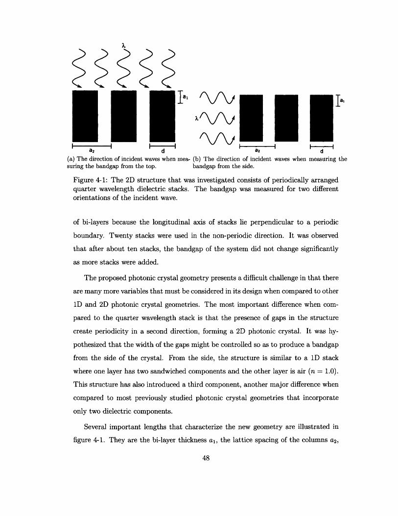
-I-
lal /VV Ial
a 2 d a2 d
(a) The direction of incident waves when mea, (b) The direction of incident waves when measuring thesuring the bandgap from the top. bandgap from the side.
Figure 4-1: The 2D structure that was investigated consists of periodically arrangedquarter wavelength dielectric stacks. The bandgap was measured for two differentorientations of the incident wave.
of bi-layers because the longitudinal axis of stacks lie perpendicular to a periodic
boundary. Twenty stacks were used in the non-periodic direction. It was observed
that after about ten stacks, the bandgap of the system did not change significantly
as more stacks were added.
The proposed photonic crystal geometry presents a difficult challenge in that there
are many more variables that must be considered in its design when compared to other
1D and 2D photonic crystal geometries. The most important difference when com-
pared to the quarter wavelength stack is that the presence of gaps in the structure
create periodicity in a second direction, forming a 2D photonic crystal. It was hy-
pothesized that the width of the gaps might be controlled so as to produce a bandgap
from the side of the crystal. From the side, the structure is similar to a 1D stack
where one layer has two sandwiched components and the other layer is air (n = 1.0).
This structure has also introduced a third component, another major difference when
compared to most previously studied photonic crystal geometries that incorporate
only two dielectric components.
Several important lengths that characterize the new geometry are illustrated in
figure 4-1. They are the bi-layer thickness al, the lattice spacing of the columns a2,
48
and the diameter or width of each column, d. Investigating the effects of each variable
independently would be time-consuming, but luckily the system can be simplified by
nondimensionalizing several variables. It can be derived from Maxwell's equations
(and was also verified computationally) that doubling the system size produces the
exact same optical response for wavelengths twice as large - there is no inherent length
scale associated with Maxwell's equations. Thus a good approach to characterize the
structure is to nondimensionalize the system by fixing the ratio l, which can bea2'
thought of as an aspect ratio, and to vary the column width, d. The ratio d willa2
be referred to as coverage fraction, because it represents the fractional area that the
dielectric stacks occupy. For all badgaps presented below, a = 23 = .7667. This ratioa2 30
was chosen somewhat arbitrarily because it allowed for integer values of gridpoints for
both dimensions and wavelengths. It is likely that the structure will behave differently
as the ratio is varied, and the effect of the ratio will be the subject of future work.
Wavelengths are reported in a nondimensional unit of A where A is the wavelength
and al is the bi-layer thickness. characterizes a dielectric stack because scaling theal
layer thickness will equally scale the quarter wavelength of the stack.
For all 2D studies, the largest realistic dielectric contrast, , was used. A large
dielectric contrast allows for fewer bi-layers in the simulation of a photonic stack.
Although the 1D stack is by definition infinite, a finite stack of high contrast can
have just a few bi-layers and approximate an infinite stack. Maxwell's equations are
also dielectric contrast independent; doubling the dielectric constants of the system
will produce the same behavior for wavelengths half as large. However, because the
system being investigated contains 3 different dielectrics and nair cannot be changed,
the absolute values of the dielectric constants will come into play. The effect of
absolute index of refraction remains to be investigated. Silicon has one of the highest
indices of refraction for a commonly used dielectric at n = 3.6, and air has the lowest
possible constant at n = 1. Thus for the 2D system described in the next section,
a dielectric contrast of was used. The values used for n and n2 were 4.5 and
1.25 respectively. These values were chosen with n2 > nair so that the system would
contain three components. nl = 4.5 is high for an index of refraction, but it not
49

completely unrealistic and could be lowered if the number of bi-layers in the stacks
was increased.
Unlike other photonic crystal structures that are known to posses full bandgaps,
this new geometry has the advantage of potentially being easy to manufacture. Meth-
ods are available to make 1D dielectric stacks via deposition processes, and gaps could
conceivably be introduced into the the structure with a masking process or with a
focused ion beam. The design also naturally lends itself to the introduction of con-
trolled defects. For a 1D quarter wavelength stack, a defect is created by changing the
thickness of one of the dielectric layers, and such a defect could be easily introduced
during deposition of the layers. The defect layer creates a localized region where
frequencies within the photonic bandgap can exist without decaying. The quarter
wavelength stacks on each side of the defect essentially act as mirrors and prevent
the light from escaping from the defect.
This new photonic crystal geomentry may be suitable for some special applica-
tions. The FDTD method has been used to study micropost microcavities[20], which
are quarter wavelength stacks with a defect layer that acts as a cavity. The optical
thickness of the defect layer can be controlled to define the wavelength of light that is
trapped. If a quantum dot is placed in the defect cavity, the quantum dot exhibits en-
hanced spontaneous emission of a stream of single photons[21]. Single photon sources
are necessary for quantum cryptography and quantum computation, and it has been
proposed that strategically designed arrays of microposts might be a candidate for a
new low-threshold, tunable lasing material. Such a structure with defects might also
be useful as a solar collector or tunable light filter.
4.2 2D Photonic Crystal Performance
Bandgaps for the 2D structure were computed using the software described in section
3.5, and important bandgaps are displayed in appendix A. Joannopoulos observed
that TE band gaps are favored in a lattice of isolated high-e regions, and TM band
gaps are favored in a connected lattice[12]. Kong also remarks that for a solid dielec-
50

tric surface, TE waves generally reflect more than TM waves[5]. The structure being
investigated consists of isolated stacks, and both trends was observed during TE and
TM calculations of the top and side bandgaps.
Following the observations of Joannopoulos and Kong, the top TM bandgap is
observed to disappear rather quickly as the periodic gaps are introduced and the
structure becomes disconnected (figure A-2). At a coverage fraction of 70% for in-
stance, the bandgap has already closed. For the TE mode however (figure A-1), the
top bandgap persists and remains wide, even at low coverage fractions. A sizeable
bandgap was found to exist at coverage fractions as low as 10%, as is shown in fig-
ure A-lj. The progression of the bandgap with decreasing coverage shows that the
bandgap narrows and shifts toward shorter wavelengths: a blue shift. The fact that
the bandgap persists reveals the suprising result that, for the top-down TE case, the
structure is a perfect dielectric mirror even though it is full of holes in the direction
of propagation of the incident light. For the 10% coverage case, consider that the
structure is 90% empty space yet maintains a bandgap. The same phenomenon is
observed in 3D in chapter 5, and an explanation for why a structure with such a large
fraction of holes may act as a perfect mirror is ventured in chapter 6.
Appendix figures A-3 and A-4 show bandgaps calculated from the side for both
TE and TM modes, respectively. The shape of the reflectivity plots is noticeably
different from the side than from the top for both polarizations. The TE plots in
figure A-3 show the existence of several bandgaps that persist over a wide range of
coverage fractions. These gaps appear to merge as coverage is decreased. As with
the top bandgap, the gaps appear to shift toward the blue frequency range as the
coverage fraction is decreased. The primary gap is the widest for coverage fractions
around 40%. The trends for TM mode from the side (figure A-4) are similar to TE.
Multiple bandgaps are observed at a few coverages but, unlike the TE case, the higher
order gaps are narrow and the primary gap is spike-shaped. Like the TE side gap,
the TM gap also appears to be largest around 40% coverage. However, unlike TE,
the gap does not quite open at very high and very low coverages.
For the structure to have a complete 2D bandgap, it is necessary for a gap to exist
51

TE bandgaps for a 2D dielectric stack array with coverage fraction of.3
0.8
0.6
0.4
0.2
a2 3 4 5 6 7 8
Nondimensionalized wavelength (. /a )
Figure 4-2: A comparison of the top and side TE bandgaps for the 1D array ofdielectric stacks with a coverage fraction of 30%. Significant overlap is observed forTE mode, suggesting that the 2D structure may have a full TE bandgap.
for both top and side directions and for both polarizations over the same frequency
range. Additionally, the gap must exist for all angles of incidence. Although angle
of incidence was not varied (all calculations were performed for normal incidence), it
can be concluded that this 2D structure does not have a complete gap because there
is no coverage fraction for which the top and side TM bandgaps overlap at a normal
angle of incidence. The top TM bandgap provides the most difficulty, appearing only
at high coverages where the side bandgaps are small or non-existant.
Significant overlap for the two TE bandgaps is observed and it is possible that
the structure may have a complete TE 2D bandgap. Figure 4-2 shows an overlay of
the two directional bandgaps for the coverage fraction of 30%, which produced the
largest overlap. The overlapping region is highlighted with a grey bar. The fractional
width of the overlapping region is approximately 30%, making it a very wide overlap.
Generally, a bandgap is considered to be wide when its fractional width, as measured
by dividing the width of the bandgap by the value at its center, exceeds 10%. The
TM side bandgap overlaps both TE gaps a small amount at 30% coverage, and it is
possible that optimizing the aspect ratio of the system might permit this overlap to
be increased. However, I am pessimistic that any dimensional changes could be made
that will maintain the top TM bandgap to low coverage fractions.
52
!~1 ' -'~l\ 'ntaonI top --. I
~~~~I~~~ -
Ii i ~I r

Chapter 5
3D Dielectric Structures
5.1 A new 3D structure
A 3D structure was designed and analyzed using the same strategy as for the 2D
structure of section 4.1. The 3D structure, illustrated in figure 5-1, is a square lattice
of rectangular-column quarter wavelength stacks. Rectangular columns were chosen
over cylindrical columns because the rectangle does not exhibit aliasing effects when
scaled on a square grid. If cylindrical columns were represented using the current
gridding scheme for instance, the grid resolution would be yet another variable to
consider. Cylindrical columns with a large diameter would be well resolved when
drawn on a rectangular grid, but those with a small diameter would be blocky and
rough. The error associated with representing a cylindrical column on a rectangular
grid for FDTD simulations is unknown, although it has been observed that perhaps
aliasing does not have much of an effect and instead it is the periodicity of the
structure that characterizes the bandgap[l]. Nonetheless, square columns were used
to eliminate this potential source of error.
Simulating the structure in 3D presents several challenges not encountered in 2D.
First, the running time of the simulation increases due to the fact that the number of
gridpoints has increased. The 2D simulations only had to store three field components
(Either Hz, H,, and E, for TE mode, or E., E,, and Hz for TM mode), but for 3D
all six field components (x, y, and z for both f and H ) must be stored. Thus in
53
addition to their being more grid points for the third dimension, the equation for
evolving each grid point contains more terms and is slower to compute.
Figures 5-lb and 5-1c show the dimensions that were used to characterize the 3D
structure. The bird's eye view shows that the the columns have a square cross-section
and are arranged on a square lattice. There is 4-fold rotational symmetry along this
axis. This means that, if the longitudinal axis of the columns is aligned along the
z-axis as shown in the figure, it is not necessary to distinguish between the x-axis
side bandgap and y-axis side bandgap because of symmetry. Thus the term "side
bandgap" now refers to either the x or y axis.
4-fold rotational symmetry simplifies the system considerably. Without it, the
columns would be characterized by two widths, there would be two lattice constants,
and bandgaps along all three axes would have to be calculated. Symmetry also allows
the system to be nondimensionalized and compared to its 2D counterpart. The 3D
structure was nondimensionalized in the same manner as the 2D structure (section
4.1) by setting the aspect ratio = 23. As with the 2D structure, plane wave
wavelengths are presented in nondimensional units of A, but in 3D the coverage
becomes (ad The squaring operation emphasizes that in 3D the the stacks have a
2D cross-section, whereas in 2D the stacks had a 1D cross-section.
Although TE and TM modes were defined as 2D concepts in section 3.2, analogous
modes exist in 3D but are dependant on the point group symmetry of the system.
Because of the superposition principle of electromagnetic waves, it is possible to break
any incident wave into two orthogonally polarized components. Consider the plane
wave illustrated in figure 5-lb that is incident upon the top of the array of stacks: the
Poynting vector of the plane wave is parallel to the z-axis of the columns, with the
E field and H field in the x-y plane. The dielectric structure has 4-fold symmetry
around the z-axis. As the E and H fields are rotated about the z-axis, the dielectric
environment they experience will change with the degree of rotation. After a rotation
of 90°, the two fields will be back in identical positions. Because of this rotational
symmetry, these two orthogonal polarizations must be equal. Thus the reflectivity of
any arbitrarily oriented polarization along the 4-fold axis will be isotropic.
54

The side configuration has 2-fold rotational symmetry along the incidence axis
(either x-axis or y-axis), and thus two polarization conditions exist. If E and H are
restricted to being parallel to principle axes for simplicity, one condition puts the E
field along the longitudinal axis of the columns (Ez-polarized), and the other puts
the H field along the longitudinal axis (Hz-polarized). Because of the principle of
superposition of waves, all other polarization angles can be broken into components
that are Ez-polarized and Hz-polarized.
5.2 3D Photonic Crystal Performance
The 3D structure, like its 2D counterpart, has indices of refraction of nl = 4.5 and
n2 = 1.25, and bandgaps for the top and side configurations of the structure can
be found in Appendix B. As discussed in the previous section, there is no need
to specify polarization for the top configuration due to the 4-fold symmetry axis,
but two polarizations, E and Hz, exist when measuring the side bandgap. The
trends observed for the 2D structure appear in analysis of the 3D structure. The
top bandgap (figure B-1) exists for high coverage fractions, and decreases in width
and shifts toward lower wavelengths as coverage is decreased. Because the top gap
persists with decreasing coverage, it suggests that an array of stacks may be a perfect
dielectric mirror under certain conditions. When compared to the 2D top bandgaps
in Appendix A, the 3D bandgaps appear qualitatively similar to the TE gaps at high
coverage, and similar to the TM gaps at low coverage. Recall that coverage fraction
for the 3D structure is () , so coverage fraction should not be used to directly
compare 2D and 3D results. Nonetheless, it is interesting to look for qualitative
similarities in the shapes of the 2D and 3D bandgaps. Whether there is any physical
explanation for such similarities remains to be investigated.
Bandgaps for Hz polarization are shown in figure B-2 and for Ez polarization
in figure B-3. The bandgaps for the two polarizations appear to be qualitatively
similar, with a primary bandgap opening at roughly 3 wavelengths for middle to low
coverages. The Hz gap is wider than the Ez gap and is also sustained over a larger
55
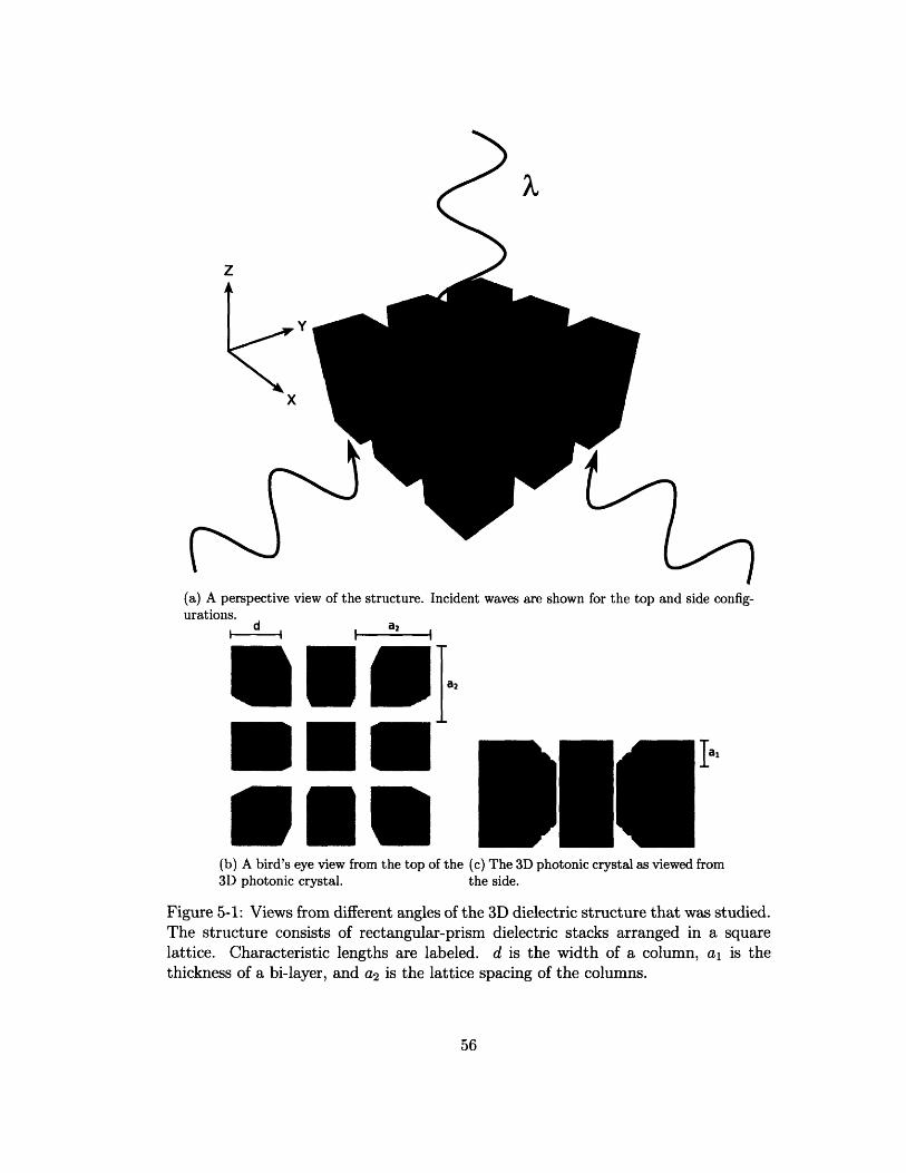
x
z
Y
x
(a) A perspective view of the structure. Incident waves are shown for the top and side config-urations.
I d I a2 I
a2
-I.
Iai
(b) A bird's eye view from the top of the (c) The 3D photonic crystal as viewed from3D photonic crystal. the side.
Figure 5-1: Views from different angles of the 3D dielectric structure that was studied.The structure consists of rectangular-prism dielectric stacks arranged in a squarelattice. Characteristic lengths are labeled. d is the width of a column, al is thethickness of a bi-layer, and a2 is the lattice spacing of the columns.
56
I
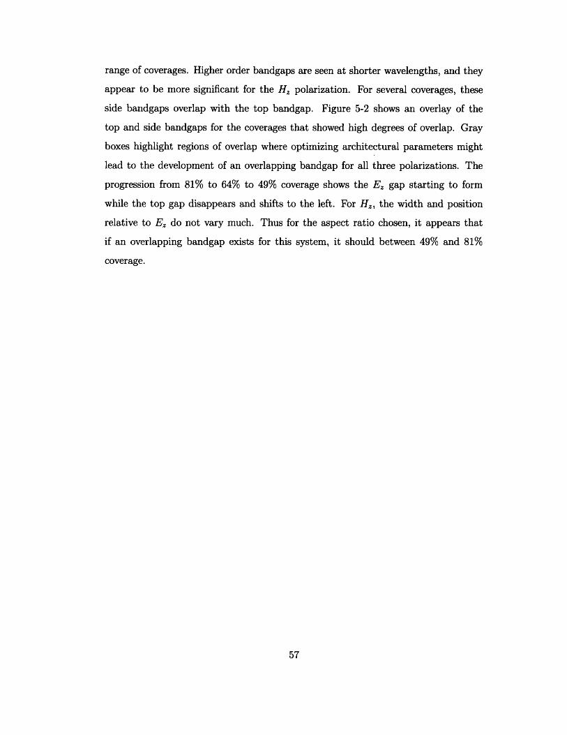
range of coverages. Higher order bandgaps are seen at shorter wavelengths, and they
appear to be more significant for the Hz polarization. For several coverages, these
side bandgaps overlap with the top bandgap. Figure 5-2 shows an overlay of the
top and side bandgaps for the coverages that showed high degrees of overlap. Gray
boxes highlight regions of overlap where optimizing architectural parameters might
lead to the development of an overlapping bandgap for all three polarizations. The
progression from 81% to 64% to 49% coverage shows the Ez gap starting to form
while the top gap disappears and shifts to the left. For Hz, the width and position
relative to Ez do not vary much. Thus for the aspect ratio chosen, it appears that
if an overlapping bandgap exists for this system, it should between 49% and 81%
coverage.
57
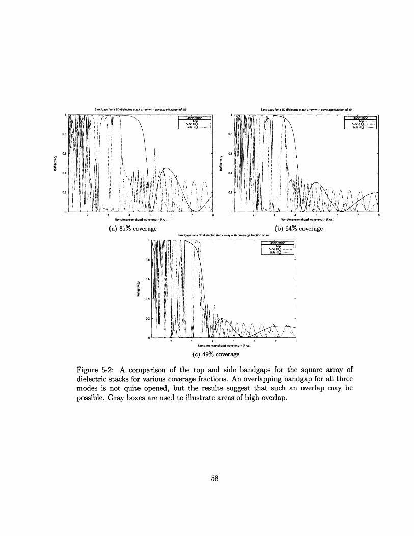
Bandgaps for a 3D dielectric stack array with coverage fraction of .81
0.8
0.6
0.4
0.2
3 4 5 6 7 6 2 3 4 5Nondimensionalhzed wavelength (i./a, Nondimensionalized wavelength (;. /a,)
(a) 81% coverage (b) 64% coverageBandgaps for a 3D dielectric stack array with coverage fraction of .49
0.8
0.6
0.4
0.2
0
i !jl i ' ldeiH--::~ l-
li'i~iiii~ ililIi~Sid']i I:0 SId.(E ........
~ iit ,.j '~ ~ ' :'T'
Io: ~ ~ ~ ~ I *I. i
2 3 4 5Nondimensionalized wavelength (;i/a.)
(c) 49% coverage
6 7 8
Figure 5-2: A comparison of the top and side bandgaps for the square array ofdielectric stacks for various coverage fractions. An overlapping bandgap for all threemodes is not quite opened, but the results suggest that such an overlap may bepossible. Gray boxes are used to illustrate areas of high overlap.
58
0.8
0.6
0.4
0.2
B..dgap f 3 dialect,,, m.,* .,,.y Mith -,werg fwb. &.64.~
DII

Chapter 6
Discussion
6.1 Discussion of results
The results of chapters 4 have several exciting consequences. The first is that an
array of dielectric stacks has unexpected optical properties, and there is potential for
a structure with overlapping bandgaps along different axes and potentially a complete
bandgap. It was also found that an array of dielectric stacks exhibit a bandgap from
the top, despite the fact that the structure is partially hollow. A plausible explanation
may exist for why a structure with holes completely through it can be a perfect mirror,
and it is possible that the physics may be exploited to make a variety of interesting
devices. If the distance between the gaps is roughly the same size as the wavelength
of the incident wave, the incident wave will be diffracted as it passes though the
gap. When the light is diffracted, it will spread out as it enters the structure and
eventually enter one of the dielectric columns. Because the columns are quarter
wavelength stacks that reflect frequencies of light that lie within the bandgap, they
will perfectly reflect the light that is diffracted into them. If the dielectric constants
of the components in the stack are large, the light will tend to be confined within the
column due to the principle of total internal reflection. The columns are surrounded
by air with the lowest possible dielectric constant, and electromagnetic waves tend to
be be confined within high refractive index materials. This confinement within the
column may result in the light being completely reflected.
59

A second observation is that the structure might be improved by switching to
a hexagonal lattice or by inverting the structure so that it consists of arrays of air
columns in a 1D dielectric stack. Simulating cylindrical columns may also prove
advantageous. Joannopoulos observed that, for 2D photonic crystals, a square lattice
of dielectric circles did not have a TM bandgap, but a hexagonal lattice of circles or
a hexagonal lattice of air holes possessed a complete 2D photonic bandgap[12].
The third observation is that these structures are geometrically simple and finite
yet exhibit large bandgaps. This suggests that useful structures might be able to
be manufactured for applications, and controlled defects could be introduced very
easily and may be used to optimize the behavior of the structure. When compared
3D photonic crystals that are known to have complete bandgaps such as dielectric
spheres on a diamond lattice[22], the Yablonovite structure[13], or several of the
triply periodic minimal surfaces[23], the stack array geometry is much simpler to
manufacture and might be modified to be self-supporting. The columns are not self-
supporting since they are surrounded by air, but it seems reasonable that if they
contain enough bi-layers, they could be attached to a substrate with no effect on the
optical performance of the crystal. Alternatively, a structure consisting of arrays of
air columns in a 1D stack would be self-supporting.
6.2 Discussion of software
6.2.1 Philosophy on Reusable Software
One of the goals of this work has been to develop a versatile toolbox of code that can
be used for a variety of simulations in place of developing many smaller stand-alone
programs. Often, scientific simulations are written such that the actual simulation
code, which is generally quite short, is embedded among housekeeping type functions
such as input/output routines, parsing routines, mathematical procedures, etc. Al-
though this approach is often quick to yield results, it is not at all modular and is thus
difficult to debug, modify, and re-use, and, most importantly, produces code that is
60

difficult for other scientists to use and understand. Considerable effort was invested
in this this work to make sure the software was written cleanly and efficiently and is
re-usable.
The design of this software is based on a grid object that can be used to write short
libraries of code (similar in nature to shell scripts) that solve finite difference prob-
lems on a single processor or in parallel. Currently, libraries implementing Maxwell's
equations, Cahn-Hilliard dynamics, and diffusion have been written, and the libraries
themselves are short and easy to comprehend. The grid framework consists of a C++
object class and a collection of optimized macros and functions defined to operate
on the grid. Grids can be written and loaded from files and there are functions that
initialize the grid, set the boundary conditions, and execute macros that calculate
spatial derivatives, laplacians, gradients, divergence, curls, cross products, dot prod-
ucts, and other mathematical operations. When run in parallel, the grid objects keep
track of their neighboring grids and exchange boundary values at the end of each
timestep.
Use of the grid objects will allow different simulations to be coupled. A grid object
could be used for a Cahn-Hilliard phase-field simulation, and then mapped to another
grid of dielectric constants which could then be analyzed using the Maxwell equations
library. The result would be a simulation that measures the optical properties of a
system undergoing Cahn-Hilliard evolution.
6.2.2 Implementation of Fourier Analysis
Application of Fourier analysis to the electromagnetic simulations presented in this
work is an important next step that should speed up the calculation of photonic
bandgaps by at least two orders of magnitude (see section 2.3). Such a speed up
will make investigation of angle of incidence in 3D possible. The current approach
for calculating reflectivity involves iterating over a range of incident wavelengths and
measuring reflectivity from the steady-state conditions that result at each wavelength.
With this method, a new simulation is run for each wavelength considered. This ap-
proach is easy to understand and implement, but very inefficient. An entire reflectivity
61

bandgap could be calculated from one simulation of a Gaussian pulse because, unlike
a plane wave that contains only one frequency, a pulse contains a wide frequency
spectrum. The Fourier transform of the response of the dielectric structure to the
pulse can be examined to determine the reflected power for each frequency contained
in the pulse. The response function of the system can also be used to determine how
the system will respond to any other input signal through the use of a convolution
[Eq. 2.21.
6.2.3 A Monte Carlo Method for Optimizing Bandgaps
The problems studied in this work may lend themselves to the application of a Monte
Carlo optimization method for finding geometries with unique optical properties.
Analysis of the 3D structure in this work showed, among other things, that many
variables characterize a system that behaves in unexpected ways. The selection of
dimensions and values for variables was, in some cases, arbitrary, and it is possible that
important behaviors are being missed. Additionally, much time is spent preparing
and managing input files and then plotting and analyzing results. Thus a Monte Carlo
method could be implemented to help automate the process of optimizing bandgaps
of dielectric structures. It would be necessary to write code to generate input files
and then analyze their bandgaps, perhaps by measuring the width of the bandgaps
and noting their centers. This code would then assign a ranking to the structure after
considering the bandgap at other angles of incidence and polarizations. A random
parametric perturbation would then be made to the structure, such as a change in
aspect ratio, coverage, or dielectric constants, and a new ranking would be calculated
and parametric derivatives obtained. If the new structure showed improvement, it
would be kept some fraction of the time related to the amount of improvement it
showed, and the process would be repeated until a more desirable structure is found.
62
6.2.4 Public software release
A preliminary public release of the software with an open source license is anticipated
in the near future after the code can be cleaned up and packaged for other users. The
software will be available for Windows, Linux, and Mac OS. The initial release will
contain libraries for running finite difference electromagnetic simulations, phase-field
simulations, and diffusion simulations in parallel. The eventual goal of the software
will be to couple these simulations with other methods such as finite element and
meshless techniques to solve complex physics problems.
6.3 The Future: Multi-physics Modeling
Materials behave in complex, extremely non-linear ways, and there are important
and novel material phenomenon that cannot be observed except through coupling of
properties. There is a class of materials including ferroelectrics and shape memory
alloys, where the application of one field could change a material's structure or ge-
ometry to effectively produce a different material. These interesting behaviors are
derived from coupled interactions within the materials. The possibility of coupling
many optical, electrical, and mechanical properties together in a computer simulation
toolbox of reusable code will aid in the development of active materials: materials
that react to their environment in intelligent ways and could be used to make novel de-
vices, switches, and sensors. Multi-physics modeling appears to be an important field
of scientific study in the computational domain in which there space for significant
progress to be made.
It has shown that the realistic bounds on materials property space have been
reached, and there is evidence to suggest that it is better to develop clever mixtures
and geometrical configurations of materials that optimize multiple properties rather
than looking for new materials that meet a strict list of design requirements[24].
Composite materials such as fiberglass, steel-reinforced concrete, and carbon-fiber
weaves are being utilized for their improved mechanical properties. Two materials,
each with a desirable mechanical property, are blended to create a new material
63
with the desirable properties of each of its components. Multi-physics computational
modeling seeks to expand upon this idea to create materials with novel behavior by
solving simultaneously for complex interactions between mechanical, optical, elec-
trial, magnetic, thermal, ordering, and symmetry properties. Materials that will be
particularly interesting to simulating include piezoelectrics, shape memory materials
(exotic shape memory polymers that react to light have recently been discovered[25]),
photonic crystals that can be used to mold the flow of light[26, 27], solar cells, liquid
crystals, semiconductors, and magnetic materials.
The study of multi-physics will open the door to the development of active mate-
rials: materials that, through coupling, react intelligently to their environment and
can be used as novel sensors. These could be things like a light filter that can be
tuned by an applied stress or electric field, materials that have a memory of their
environment, or materials that respond in unique ways to light, sound, heat, or other
fields. Novel geometrical constructions of these materials, such as triply periodic bi-
continuous minimal surfaces, which have been shown to optimize multiple properties,
will also be investigated[23, 28].
64

Appendix
Reflectivity band diagrams for the
2D structure
65
A
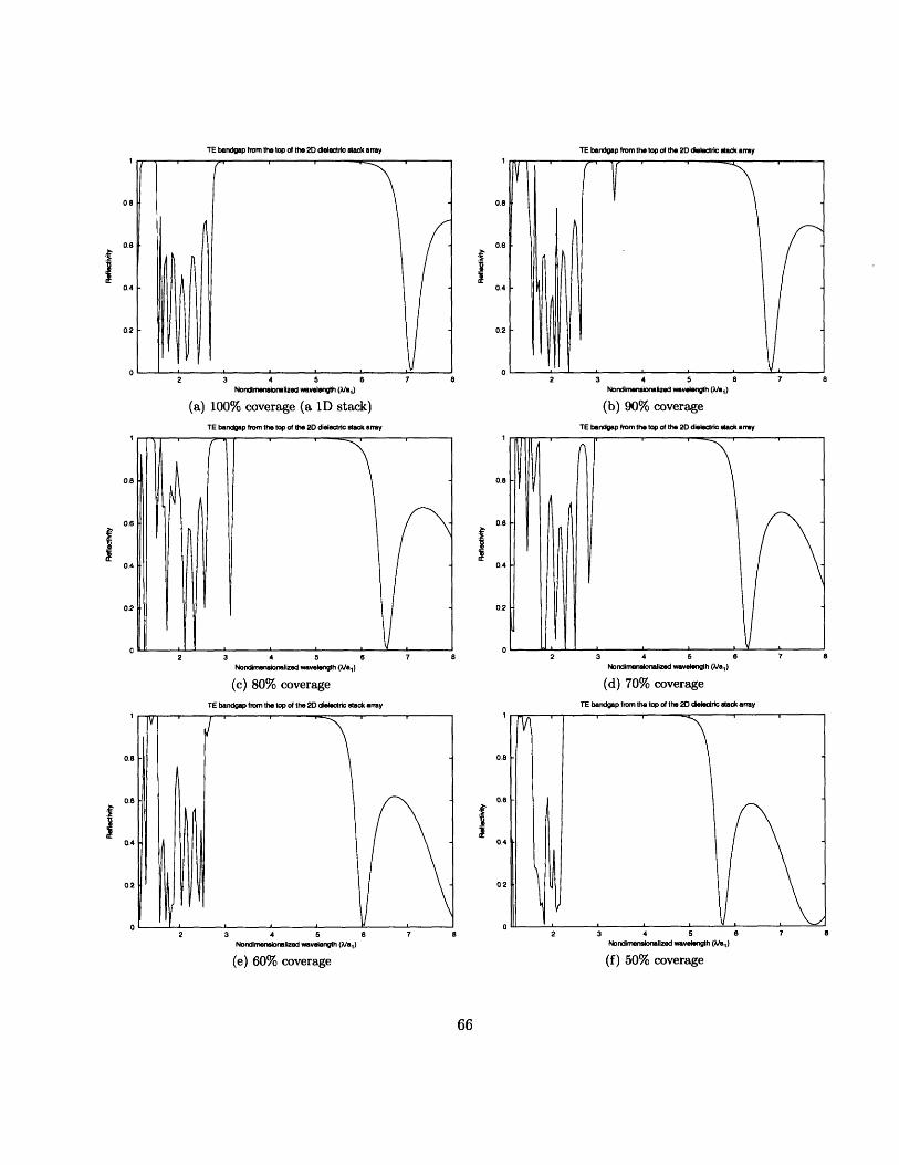
TE bandgap from the top of the 2D dielectric stack array
I
2 3 4 5 6 7 8Nondimeneionalized wavelergth (a , )
(a) 100% coverage (a 1D stack)
TE bandgap from the top of the 2D dielectric tack array
2 3 4 5 6 7 8
Nomndimnionalized wavelength (Ja/1)
(c) 80% coverage
TE bandgap from the top of the 2 dieleotric stack array
0.
0.8
0.6
0.4
02
Nondmenrionalized wavelength (a,)
(b) 90% coverage
TE bardgap from the top of the 2D dielectric sack array
Nondimenlonalized wavelength ())
(d) 70% coverage
TE bandgap from the top of the 2D dielectric Mack array
3 4 5 8 7 8 2 3 4 5Nondimernsionalized wavelength 0Jal) Nondimenloalized wavelength (A/a,)
(e) 60% coverage (f) 50% coverage
66
08
0.8
0.4
0.2
n1
0.8
0.8
0.4
0.2
Cl
1
0.8
0.6
0.4
0.2
TE bardigap from the top of the 2 dieledric, stac aay
fIN

TE bandgap from the top of the 2D diledtric stack array
Nondim ornalizad wavelength (A/a,) Nondimenonalized wavelangth (A/a,)
(g) 40% coverage (h) 30% coverage
TE bandgap from the top of the 2D delectric stack armray TE bandgap from the top of the 2D dielectri ack army
I
Nondimenaionalized wavelenglh (Jal)
(i) 20% coverage
0.8
f0.6
0.4
0.2
0 2 I 5 l- 2 3 4 5 6 7 a
Nondimanrioalized wavelength (/Jal)
(j) 10% coverage
Figure A-1: TE bandgap from the top direction of the 2D array of dielectric stackswith n = 4.5 and n2 = 1.25 for various coverage fractions (d/a 2 ).
67
0.
0.
0.
0.
TE bandgap from the top of the 2 cadc sta ay
I
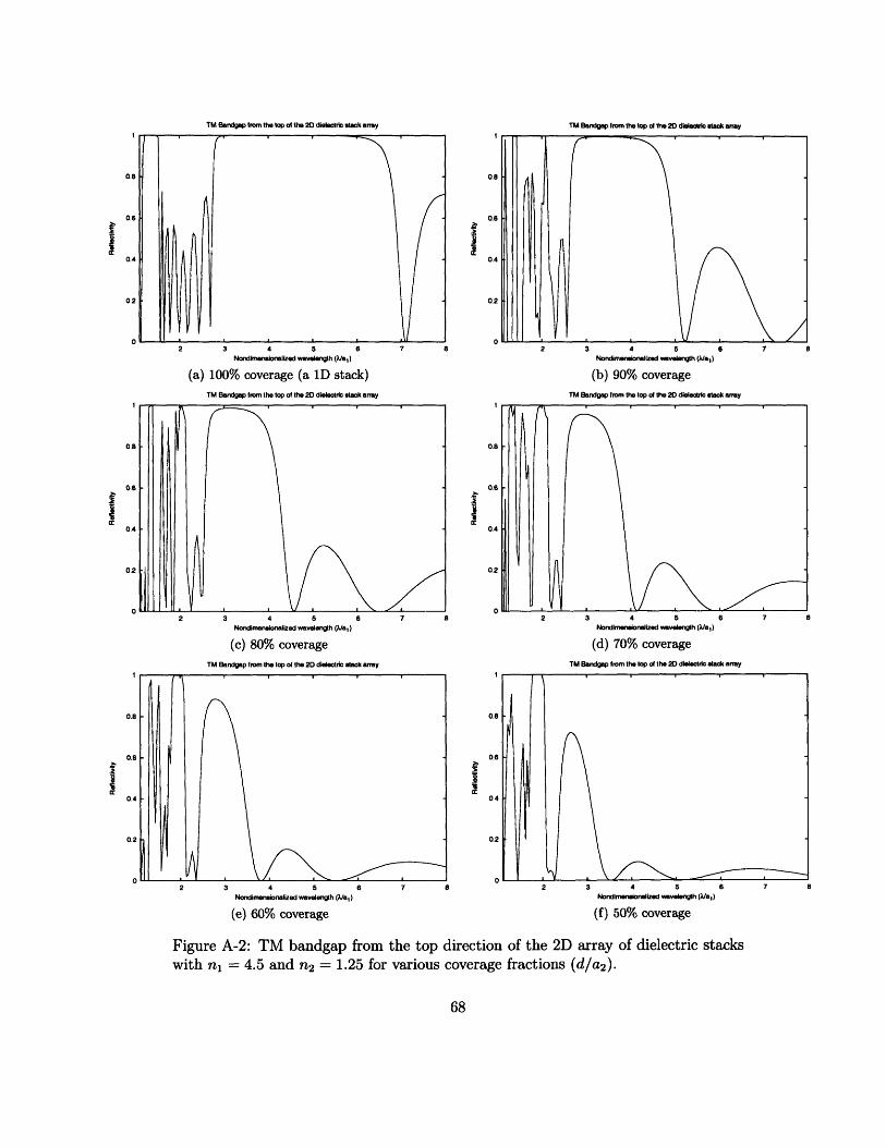
TM Bandgp from the top o the 2D die eoti stak array
3 4 5 6Nodmeionalized wavelength (a 1)
(a) 100% coverage (a 1D stack)TM Bandgap from the top of the 20 dieleotic stack aray
3 4 5 6Nondimenionalizd wavelength (Ja )
(c) 80% coverage
TM Bandgp from the top of the 2D deleotric tack aay
0.8
.5
1
0.6
0.4
0.2
0
1
0.8
0.6
0.4
0.2
8
2 3 4 5 6Nondimnionalizd wavelength (a 1)
(b) 90% coverageTM Bandgap from the top of the 2D dielecric ta aamy
2 3 4 5 6Nondimenionaizd wavelength (Aia)
(d) 70% coverage
TM Bandgap from the top d the 20 diectrc etaok army
2 3 4 5 6 7 8 2 3 4 5Nondime-ionaalizd wavelengh (A/a1) Nondimenlionalized wavelength (al)
(e) 60% coverage (f) 50% coverage
8
8
Figure A-2: TM bandgap from the top direction of the 2D array of dielectric stackswith nl = 4.5 and n2 = 1.25 for various coverage fractions (d/a 2 ).
68
0.8
0.6
0.4
0.2
tl
0.8
i0.6
0.4
0.2
0
1
0.8
2Icc
0.6
0.4
0.2
TM Bandgap Irmn the top od the 2D die in tack amay
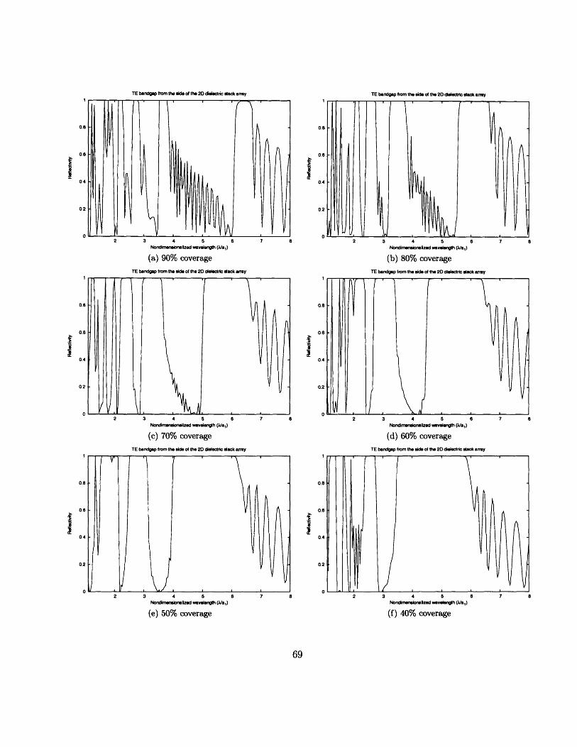
TE bandgap from the side of the 2D delric ack arramy
f
2 3 4 5 6 7 8Nondimenrioalized wavelength (J/a,)
(a) 90% coverage
TE bandgap from the ide of the 20 dielectric slack array
2 3 4 5 6 7 8Nondimrionalized wavelength (al)
(c) 70% coverage
TE bandgap from the side of the 20 dielectric stack array
2 3 4 5 6 7 8Nondimenrionalized wavelengh (/a,)
(e) 50% coverage
69
Nondimnrionalized wavelength (Ja l )
(b) 80% coverageTE bandgap from the ide of the 2 dielectric ack array
Nondimerminalized wavelength (/a 1 )
(d) 60% coverageTE bandgap from the side of the 20 dielectric stack array
2 3 4 5 6Norndimeionealzed wavlengh (/a,)
(f) 40% coverage
0.8
0.6
04
02
o
I
TE bandgap from the dle of the 2 dieric etack army
-f
.fI
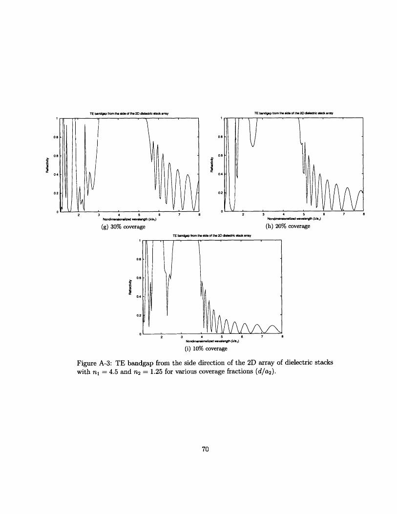
TE bandgap from the side of the 2D dielectric Mack array
.5I
Nondimenerionalized wavelength (/a) Nondimenalized wavelength (/a)
(g) 30% coverage (h) 20% coverage
TE bandgap from the side of the 2D dielectric Mstac array
.tI
2 3 4 5 6 7 8Nondimenuionalized wavelength (;Vat)
(i) 10% coverage
Figure A-3: TE bandgap from the side direction of the 2D array of dielectric stacks
with nl = 4.5 and n2 = 1.25 for various coverage fractions (d/a 2 ).
70
08
0.8
:f
04
0.2
0
TE banrdgap from the side of the 2D dielectric stack array

TM Bandgap from the kide of the 2D dielectric sack arrayI I , i _
3 4 5 6Nor irtmeneiorSized waverth (Ja,)
(a) 80% coverage
TM Bandgap from the side of the 2D dielectric stack array
2 3 4 5 6Nondmerionalized wavtnh (a 1)
(c) 60% coverage
1
0.8
.8I
0.6
04
0.2
08
I
8
2 3 4 5 6Norldmeruioaized wavllth (Ja,)
(b) 70% coverage
TM Bandgep from the ide of the 2D dielectric stack aray
7 8
4 5 6Nondimenionalized wavelength (al)
(d) 50% coverage
71
0.8
0.6
0.4
0.2
0
1
0.8
I
0.6
0.4
0.2
TM Bandgap from the side of the 2D dielectric stack array

TM Bandgap from the side of the 2D delectric stack array
3 4 5 6 7 8Nondimenrionalized wavelength (a,)
(e) 40% coverage
TM Bandgap from the side of the 2D dielectric Mtack aray
4 5 6Nondimerionalized wavelength (a)
(g) 20% coverage
Figure A-4: TM bandgap from the sidewith nl = 4.5 and n2 = 1.25 for various
0.8
0.6
0.4
0.2
0
1
0.8
0.6
0.4
02
08
TM Bandgap from the sde of the 2D dielectric stack army
2 3 4 5 6 7 8Nondimeiionalized wavelenrgth (a 1)
(f) 30% coverage
TM Bandgap from the aide of the 2 dielectric stack array
2 3 4 5 6 7 8Nondimenionalized wavelengh (/a)
(h) 10% coverage
direction of the 2D array of dielectric stackscoverage fractions (d/a 2 ).
72
08
0.6
0.4
0.2
0
1
0.8
0.6
0.4
0.2

Appendix B
Reflectivity band diagrams for the
3D structure
73
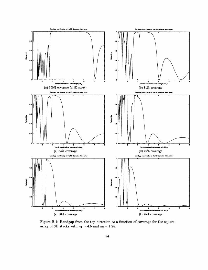
Bandgp from the top of te 30 dielectric tack anay
Nondimensionalized wavelength (Ja)
(a) 100% coverage (a 1D stack)
Bandgap from the top of the 3D dieleotric tack array
2 3 4 5 6Nondimeneionalzed wavelength (A/at)
(c) 64% coverage
Bandgap rom the top of the 3D dielecric atack array
4 5Nondimenionalied wavelength (Ja,)
(e) 36% coverage
0.8
.kI
0.6
0.4
0.2
0
0.8
c
0.6
0.4
0.2
0
1
0.8
I.j9
06
0.4
0.2
Figure B-1: Bandgap from the top direction as a function ofarray of 3D stacks with nl = 4.5 and n2 = 1.25.
2 3 4 5 6Nondimeionalized wavelength (a,)
(b) 81% coverage
Bandgap from the top of the 3D diectric tack array
2 3 4 5 6Nondimenionalized wavelngth (A)
(d) 49% coverage
Bandgap from the top ot the 30 dieletrio clack aray
2 3 4 5 6Nortmeionatlzed wavelength (Ja 1)
(f) 25% coverage
coverage for the square
74
8
8
Smdgap Irm th tp d th 3 de do r-k .- V

Bandgp Imm the side of the 3D dielectric ack aray (n=4.5, n=1 .25)
0.8
i
0.6
0.4
0.2
0
Nondimerionalized wavelength ( n2./a)
(a) 81% coverage
Hz polarized bandgap from the side of the 3D dielectric aack array
3 4 5 6Nondimeninaized wavelenglh (/a 1)
(b) 64% coverage
Hzpolarized bandgap from the eide of the 30 dieleltric tack array
Nondimenlonalized wavlengh (Val) Nondimenionalized wavelength (A/a)
(c) 49% coverage (d) 36% coverageHz polarized bandgap from the aide of the 3D dielectric atack array Hz polarized bandgap from the aide of the 30 dielectric tack array
4 0 a I z a o uNondimrmionalized wavelength (Ja) Nondimenlonalized wavength (al)
(e) 25% coverage (f) 16% coverage
Figure B-2: Hz polarized bandgap from the side direction as a function of coveragefor the square array of 3D stacks with nl = 4.5 and n2 = 1.25.
75
0.8
i
0.6
0.4
0.2
0
1
0.8
0.6
0.4
1f
(E
H plaried bndgap frwm the aide o the 3 dialeciric alsk array
x~ ^ ; R

E zpolarized bandgap Irom the aide the 3D dielectric tack aramy
0.8
0.8
0.4
0.2
2 3 4 5 6 7 8 2 3 4 5 6 7 8Nondimenionalzed wavelength (A/a) Nondimenlioralized wavdlength (A/al)
(a) 81% coverage (b) 64% coverage
E, polarized bandgap from the ide ot the 3D dielotrc clack array E zpolarized bandgap from the ide o the 3D dieectric ack amay
Nondimeraionalzed wavelength (A/)
(c) 49% coverage
E polarized bandgap from the aide o the 3D dielectric rtack array
Nondimerwionalzed wavelength (/a,)
(e) 25% coverage
0.8
fIM
0.6
0.4
0.2
0
0.8
fI
0.6
0.4
0.2
o
Nondimenioalized wavelength (A/al)
(d) 36% coverage
E, polarized bandgap from the aide of the 3D dielectric lack array
2 3 4 5 6ndmaonizd wavelength (Aal)
(f) 16% coverage
Figure B-3: E polarized bandgap from the side direction as a function of coveragefor the square array of 3D stacks with n1 = 4.5 and n2 = 1.25.
76
I
:E1
Itr
7 8l ..,.... . . , · ......... . . . . ..
E, polad-ed b.dgp -o th. id. th 3 dadric d..k -yy
A "\ - - - - - ��

References
[1] Steven G. Johnson and John D. Joannopoulos. Photonic Crystals: The Road
from Theory to Practice. Kluwer Academic Publishers, 2002.
[2] Allen Taflove and Susan C. Hagness. Computational Electrodynamics: The
Finite-Difference Time-Domain Method. Artech House, 2000.
[3] Basil Mahon. The Man Who Changed Everything. John Wiley and Sons, Inc.,
2003.
[4] John David Jackson. Classical Electrodynamics. John Wiley and Sons, Inc.,
1999.
[5] Jin Au Kong. Electromagnetic Wave Theory. EMW Publishing, 2000.
[6] Alfred Owen Aldridge. Benjamin Franklin Philosopher and Man. J.B. Lippincott
Company, 1965.
[7] Erwin Kreyszig. Advanced Engineering Mathematics. John Wiley and Sons Inc.,
1999.
[8] Marko Loncar, Tomoyuki Yoshie, and Axel Scherer. Low-threshold photonic
crystal laser. Applied Physics Letters, 81:2680-2682, 2002.
[9] Susumu Noda, Alongkarn Chutinan, and Masahiro Imada. Trapping and emis-
sion of photons by a single defect in a photonic bandgap structure. Nature,
407:608-610, 2000.
77

[10] Y Sugimoto, Y Tanaka, N Ikeda, K Kanamoto, Y Nakamura, S Ohkouchi,
H Nakamura, K Inoue, H Sasaki, Y Watanabe, K Ishida, H Ishikawa, and
K Asakawa. Two dimensional semiconductor-based photonic crystal slab waveg-
uides for ultra-fast optical signal processing devices. IEICE Transactions on
Electronics, E87C:316-327, 2004.
[11] DR Smith, WJ Padilla, DC Vier, SC Nemat-Nasser, and S Schultz. Composite
medium with simultaneously negative permeability and permittivity. Physical
Review Letters, 84:4184-4187, 2000.
[12] John D. Joannopoulos, Robert D. Meade, and Joshua N. Winn. Photonic Crys-
tals: Molding the Flow of Light. Princeton University Press, 1995.
[13] E Yablonovitch, TJ Gmitter, and KM Leung. Photonic band-structure - the
face-centered-cubic case employing nonspherical atoms. Physical Review Letters,
67:2295-2298, 1991.
[14] H. Joseph Weaver. Applications of Discrete and Continuous Fourier Analysis.
John Wiley and Sons, Inc., 1983.
[15] Kane S. Yee. Numerical solution of initial boundary value problems involving
maxwell's equations in isotropic media. IEEE Transactions on Antennas and
Propagation, 14:302-307, 1966.
[16] Jean-Pierre Berenger. A perfectly matched layer for the absorption of electro-
magnetic waves. Journal of Computational Physics, 114:185-200, 1994.
[17] Dennis M. Sullivan. Electromagnetic Simulation Using the FDTD Method. IEEE
Press, 2000.
[18] Karlene R. Maskaly. Computational Study and Analysis of Structural Imperfec-
tions in 1D and 2D Photonic Crystals. PhD thesis, MIT, 2005.
[19] David Halliday, Robert Resnick, and Jearl Walker. Fundamentals of Physics.
John Wiley and Sons Inc, 2001.
78
[20] Jelena Vuckovic, Matthew Pelton, Axel Scherer, and Yoshihisa Yamamoto. Op-
timization of three-dimensional micropost microcavities for cavity quantum elec-
trodynamics. Physical Review A, 66, 2002.
[21] Matthew Pelton, Jelena Vuckovic, Glenn Solomon, Charles Santori, Bingyang
Zhang, Jocelyn Plant, and Yoshihisa Yamamoto. An efficient source of single
photons: a single quantum dot in a micropost microcavity. Physica E, 17:564-
567, 2003.
[22] KM Ho, CT Chan, and CM Soukoulis. Existence of a photonic gap in periodic
dielectric structures. Physical Review Letters, 65:3125-3155, 1990.
[23] Alan H. Schoen. Infinite periodic minimal surfaces without self-intersections.
NASA Technical Note, 1969.
[24] M. F. Ashby. Multi-objective optimization in material design and selection. Acta
Materialia, 48:359-369, 2000.
[25] Andreas Lendlein, Hongyan Jiang, Oliver Junger, and Robert Langer. Light-
induced shape-memory polymers. Nature, 434(7035):879-882, 2005.
[26] D.N. Chigrin, A.V. Lavrinenko, D.A. Yarotsky, and S.V. Gaponenko. Observa-
tion of total omnidirectional reflection from a one-dimensional dielectric lattice.
Applied Physics A, 68:25-28, 1999.
[27] Emmanuel Centeno and David Cassagne. Graded photonic crystals. Optics
Letters, 30:2278-2280, 2005.
[28] S. Torquato, S. Hyun, and A. Donev. Multifunctional composites: Optimiz-
ing microstructures for simultaneous transport of heat and electricity. Physical
Review Letters, 89(26), 2002.
79