development of an enhanced lateral drift sensor
TRANSCRIPT
Development of an Enhanced Lateral Drift Sensor.
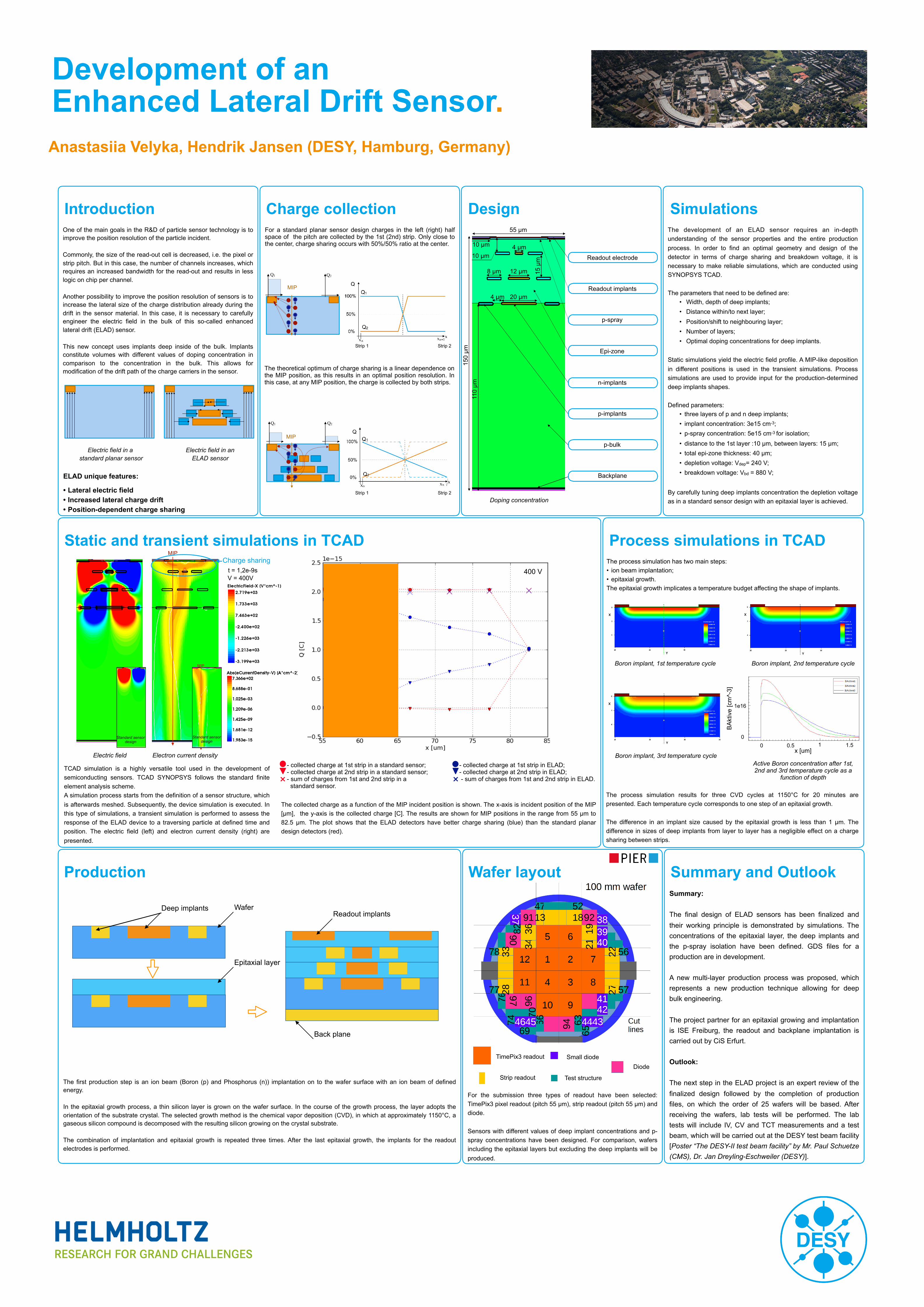
- collected charge at 1st strip in ELAD; - collected charge at 2nd strip in ELAD; - sum of charges from 1st and 2nd strip in ELAD.
IntroductionOne of the main goals in the R&D of particle sensor technology is to improve the position resolution of the particle incident.
Commonly, the size of the read-out cell is decreased, i.e. the pixel or strip pitch. But in this case, the number of channels increases, which requires an increased bandwidth for the read-out and results in less logic on chip per channel.
Another possibility to improve the position resolution of sensors is to increase the lateral size of the charge distribution already during the drift in the sensor material. In this case, it is necessary to carefully engineer the electric field in the bulk of this so-called enhanced lateral drift (ELAD) sensor.
This new concept uses implants deep inside of the bulk. Implants constitute volumes with different values of doping concentration in comparison to the concentration in the bulk. This allows for modification of the drift path of the charge carriers in the sensor.
The development of an ELAD sensor requires an in-depth understanding of the sensor properties and the entire production process. In order to find an optimal geometry and design of the detector in terms of charge sharing and breakdown voltage, it is necessary to make reliable simulations, which are conducted using SYNOPSYS TCAD.
The parameters that need to be defined are: • Width, depth of deep implants; • Distance within/to next layer; • Position/shift to neighbouring layer; • Number of layers; • Optimal doping concentrations for deep implants.
Static simulations yield the electric field profile. A MIP-like deposition in different positions is used in the transient simulations. Process simulations are used to provide input for the production-determined deep implants shapes.
Defined parameters: • three layers of p and n deep implants; • implant concentration: 3e15 cm-3; • p-spray concentration: 5e15 cm-3 for isolation; • distance to the 1st layer :10 µm, between layers: 15 µm; • total epi-zone thickness: 40 µm;
• depletion voltage: Vdep= 240 V; • breakdown voltage: Vbd = 880 V;
By carefully tuning deep implants concentration the depletion voltage as in a standard sensor design with an epitaxial layer is achieved.
- collected charge at 1st strip in a standard sensor; - collected charge at 2nd strip in a standard sensor; - sum of charges from 1st and 2nd strip in a standard sensor.
TCAD simulation is a highly versatile tool used in the development of semiconducting sensors. TCAD SYNOPSYS follows the standard finite element analysis scheme. A simulation process starts from the definition of a sensor structure, which is afterwards meshed. Subsequently, the device simulation is executed. In this type of simulations, a transient simulation is performed to assess the response of the ELAD device to a traversing particle at defined time and position. The electric field (left) and electron current density (right) are presented.
The collected charge as a function of the MIP incident position is shown. The x-axis is incident position of the MIP [µm], the y-axis is the collected charge [C]. The results are shown for MIP positions in the range from 55 µm to 82.5 µm. The plot shows that the ELAD detectors have better charge sharing (blue) than the standard planar design detectors (red).
ELAD unique features:
• Lateral electric field • Increased lateral charge drift • Position-dependent charge sharing
The first production step is an ion beam (Boron (p) and Phosphorus (n)) implantation on to the wafer surface with an ion beam of defined energy.
In the epitaxial growth process, a thin silicon layer is grown on the wafer surface. In the course of the growth process, the layer adopts the orientation of the substrate crystal. The selected growth method is the chemical vapor deposition (CVD), in which at approximately 1150°C, a gaseous silicon compound is decomposed with the resulting silicon growing on the crystal substrate.
The combination of implantation and epitaxial growth is repeated three times. After the last epitaxial growth, the implants for the readout electrodes is performed.
Readout electrode
Readout implants
p-spray
Epi-zone
n-implants
p-implants
p-bulk
Backplane
55 µm
150
µm
10 µm
20 µm
12 µm
4 µm
8 µm
4 µm
10 µm
15 µ
m
110
µm
× ×
Charge collection Design Simulations
Static and transient simulations in TCAD
The theoretical optimum of charge sharing is a linear dependence on the MIP position, as this results in an optimal position resolution. In this case, at any MIP position, the charge is collected by both strips.
For a standard planar sensor design charges in the left (right) half space of the pitch are collected by the 1st (2nd) strip. Only close to the center, charge sharing occurs with 50%/50% ratio at the center.
MIP
Production Wafer layout
TimePix3 readout
Strip readout
DiodeSmall diode
Test structure
For the submission three types of readout have been selected: TimePix3 pixel readout (pitch 55 µm), strip readout (pitch 55 µm) and diode.
Sensors with different values of deep implant concentrations and p-spray concentrations have been designed. For comparison, wafers including the epitaxial layers but excluding the deep implants will be produced.
Process simulations in TCAD
MIP
Q1 Q2
MIP
Electric field in a standard planar sensor
Electric field in an ELAD sensor
Anastasiia Velyka, Hendrik Jansen (DESY, Hamburg, Germany)
400 Vt = 1,2e-9s
Electric field Electron current density
Charge sharing
Boron implant, 1st temperature cycle Boron implant, 2nd temperature cycle
Boron implant, 3rd temperature cycleActive Boron concentration after 1st, 2nd and 3rd temperature cycle as a
function of depth
The process simulation results for three CVD cycles at 1150°C for 20 minutes are presented. Each temperature cycle corresponds to one step of an epitaxial growth.
The difference in an implant size caused by the epitaxial growth is less than 1 µm. The difference in sizes of deep implants from layer to layer has a negligible effect on a charge sharing between strips.
WaferDeep implants
Epitaxial layer
Readout implants
Back plane
BA
ktiv
e [c
m^-
3]
x [um]
1e16
0 0 0.5 1 1.5
Doping concentration
Strip 1
Strip 1
Strip 2
Strip 2
Summary and OutlookSummary:
The final design of ELAD sensors has been finalized and their working principle is demonstrated by simulations. The concentrations of the epitaxial layer, the deep implants and the p-spray isolation have been defined. GDS files for a production are in development.
A new multi-layer production process was proposed, which represents a new production technique allowing for deep bulk engineering.
The project partner for an epitaxial growing and implantation is ISE Freiburg, the readout and backplane implantation is carried out by CiS Erfurt.
Outlook:
The next step in the ELAD project is an expert review of the finalized design followed by the completion of production files, on which the order of 25 wafers will be based. After receiving the wafers, lab tests will be performed. The lab tests will include IV, CV and TCT measurements and a test beam, which will be carried out at the DESY test beam facility [Poster “The DESY-II test beam facility” by Mr. Paul Schuetze (CMS), Dr. Jan Dreyling-Eschweiler (DESY)].
Standard sensor design
Standard sensor design
The process simulation has two main steps: • ion beam implantation; • epitaxial growth. The epitaxial growth implicates a temperature budget affecting the shape of implants.
MIP
V = 400V
Q1 Q2