development of a two-dimensional tracker with plasma panel
TRANSCRIPT

CER
N-T
HES
IS-2
016-
225
21/1
2/20
16
D E V E L O P M E N T O F A T W O - D I M E N S I O N A L T R A C K E R W I T HP L A S M A PA N E L D E T E C T O R S
david reikher
Thesis submitted towards the degree of M.Sc. in physicsunder the supervision of Prof. Erez Etzion
Tel-Aviv UniversityRaymond and Beverly Sackler
Faculty of Exact Sciences
September 2015


A B S T R A C T
Plasma panel sensors are micropattern gaseous radiation detectorswhich are based on the technology of plasma display panels. Thisthesis summarizes the research that had been done on commerciallyavailable plasma display panels that were converted to plasma panelsensor prototypes and describes the construction of a two-dimensionaltracker consisting of four of those prototypes, with one-dimensionalreadout on each, used to detect tracks of cosmic muons. A largeamount of 2-point as well as 3 and 4-point tracks were detected. Quali-tative analyses as well as Pearson’s �2 tests are performed on the trackangular distribution and on a histogram of the linearity measure of3-point tracks to reject the hypothesis that these tracks result fromcompletely random panel hits. Some RF noise effects contributing tofalse positives are ruled out, while it is shown that other effects canbe ruled out only with a high-intensity minimum ionizing particlesource.
A significant part of the tracker construction was the developmentof a software toolbox to acquire and analyze signals coming fromplasma panel sensor devices, which enables long-term monitoring ofvarious aspects of the experiment. The software can be used in futuretracking experiments and in other scenarios of data acquisition fromplasma panel sensor devices. The software architecture and pulse de-tection algorithm are herein described.
iii


A C K N O W L E D G M E N T S
I had a lot of support along the way from friends, family and col-leagues, but without the help and support of some, I would not beable to finish this work.
First and foremost, I would like to express my sincere gratitude tomy thesis advisor, Professor Erez Etzion, for the guidance, the pos-itive, open-minded atmosphere, the freedom to make my own de-cisions and the constant availability and support, despite his tightschedule.
In addition, I would like to thank Meny Ben-Moshe for the count-less times he helped with the hardware setup and for being the go-toman whenever any kind of problem arose, whether related to thiswork or just for moral support and advice, July Daskal, who helpedgreatly with setting up the experiments, Dr. Yan Benhammou and Ita-mar Levi for their advice and Dr. Merlin Davies thanks to whom Ibuilt a strong basis from which I could expand. Additionally, I wantto thank Dr. Daniel Levin (UM), Dr. Peter Friedman (Integrated Sen-sors) and the entire PPS collaboration for their much needed adviceanytime I hit an obstacle.
Finally, I want to thank my family, my parents Michael and Elenafor their encouragement and for where I am today and my wife Olga,for supporting and pushing me to do what I love and (almost) nevercomplaining about me coming home late.
v


C O N T E N T S
1 introduction 1
i background 3
2 relevant physical background 5
2.1 Radiation 5
2.1.1 Beta Radiation Source 5
2.1.2 Cosmic Muons 6
2.2 Interaction Mechanism of Charged Particulate Radia-tion with Matter 6
2.3 Minimum Ionizing Particles 8
2.4 Ionization in Gases, Relevant Processes and Terminol-ogy 8
2.4.1 Interactions Between Electrons, Ions and GasParticles 10
2.4.2 Regions of Operation of Gaseous Particle Detec-tors 11
2.5 Signal Formation in Gas Detectors 16
2.6 Relevant Detector Characteristics 17
2.6.1 Dead Time 17
2.6.2 Spatial Resolution 18
2.6.3 Timing Resolution 18
2.7 Other Relevant Effects 18
2.7.1 Scattering Effects 18
2.7.2 Background Radiation 19
3 overview of plasma panel sensors 21
3.1 Operational Principles of PDPs 21
3.2 Converting PDP to PPS 22
3.3 Summary of Vishay PDP Characteristics as a PPS de-vice 24
3.3.1 Selection of an Appropriate Gas Mixture 24
3.3.2 Pulse Shape 25
3.3.3 Quench Resistance and Dead Time 25
3.3.4 Timing Resolution 26
3.3.5 Spatial Resolution 26
3.3.6 Constraints on the Efficiency of PDPs for Parti-cle Detection 28
4 preliminary theoretical tracker analysis 29
4.1 PPS-Based Tracker 29
4.2 Expected Rate of a Tracker 29
4.2.1 Rate of Muons through Two Vertically AlignedPlanes 29
vii

viii contents
4.2.2 Rate of Muons through Two or More VerticallyAligned Panels 31
4.2.3 Expected Rate of a Tracker 31
4.3 Rate of Random Coincidence 34
4.3.1 Uncorrelated Random Coincidence Rate 34
4.3.2 Random Coincidence from Correlated Noise 38
4.4 Monte Carlo Simulation of the Tracker 38
4.5 Analysis of Tracks 41
4.5.1 2-Point Tracks 42
4.5.2 3-Point Tracks 45
ii experimental procedure 47
5 preparation of the panels , electronics and the
tracker setup 49
5.1 Preparation of the Panels 49
5.2 Selection of Gas Mixture and Pressure 50
5.3 RO and HV Supply Cards 51
5.4 Determination of Operating Voltage 53
5.5 Tracker Setup 55
5.6 Terminology 56
6 daq using time multiplexing 59
6.1 DAQ Equipment 59
6.2 Implementation 59
6.3 Observation of the First Suspected Track 63
7 daq using a digitizer 67
7.1 Digitizer-PC interface 67
7.2 Digitizer-Panel Interface 67
7.3 Trigger Setup 68
7.4 Acquisition and Analysis Software 68
7.4.1 Architecture 69
7.4.2 Primary Pulse Tagging 69
7.4.3 Analysis and Monitoring Modules 73
7.4.4 Panel Hit Monitor 73
7.4.5 Panel Timing Monitor 73
7.4.6 Panel Degradation Monitor 73
7.4.7 Track Monitor 74
7.4.8 Configuration 74
iii analysis of results & conclusions 75
8 results 77
8.1 Monitoring 77
8.1.1 Monitoring the Trigger Rate and Arrival TimeDistribution 77
8.1.2 Monitoring Panel Activity 78
8.1.3 Monitoring and Analyzing Signal Waveforms 81
8.2 Analysis 83
8.2.1 Effects of Panels on Scintillators and Vice-Versa 85

contents ix
8.2.2 Effect of Panels on Each Other 85
8.2.3 2-Point Tracks 87
8.2.4 3-Point Tracks 89
9 conclusions 91
iv appendix 93
a data acquisition system 95
a.1 Triggering and DAQ Overview 95
a.1.1 Scintillator Trigger 95
a.2 DAQ Equipment Standards 96
a.2.1 NIM 96
a.2.2 ECL 96
a.2.3 VME 97
a.3 DAQ Equipment 98
a.3.1 Discriminator Units 98
a.3.2 Fan-In-Fan-Out Units 98
a.3.3 Coincidence Units 98
a.3.4 Timer Units 99
a.3.5 NIM to ECL Converter 99
a.3.6 Digital Oscilloscope 99
a.3.7 Digitizer 99
a.4 Impedance Matching and Termination 100
bibliography 103

L I S T O F F I G U R E S
Figure 1 Energy loss distribution for minimum ionizingparticles 9
Figure 2 Gaseous detector working modes 12
Figure 3 Townsend coefficient 13
Figure 4 Streamer formation 15
Figure 5 Gaseous detector cell wiring schematic 16
Figure 6 PDP structure 21
Figure 7 Vishay panel photograph 23
Figure 8 Vishay panel schematic 23
Figure 9 Pulse from Vishay panel 25
Figure 10 Vishay quench resistance plot 26
Figure 11 Vishay pulse arrival time distribution 27
Figure 12 Vishay hit map distribution 27
Figure 13 Two parallel planes representing the topmostand bottom-most panels in a tracker 30
Figure 14 Pulse and acquisition window widths 36
Figure 15 Tracker rendering 40
Figure 16 Closeup of rendered panels 41
Figure 17 Definition of �, ⇠ angles 42
Figure 18 First geometric effect distorting the track an-gular distribution 43
Figure 19 Monte Carlo generated track angular distribu-tion 44
Figure 20 Second geometric effect distorting the track an-gular distribution 45
Figure 21 Third geometric effect distorting the track an-gular distribution 46
Figure 22 Photograph of a panel attached to a tray 49
Figure 23 Effect of gas mixture on after pulsing 50
Figure 24 Photograph of a HV card 51
Figure 25 Photograph of a RO card 52
Figure 26 RO card schematic of a single line 52
Figure 27 Photograph of a flat-to-LEMO adapter 53
Figure 28 Voltage scan plot 54
Figure 29 Photograph of the tray holder for the tracker 55
Figure 30 Photograph of the tracker setup 56
Figure 31 Schematic of trigger and DAQ implementationfor time multiplexing 60
Figure 32 Expected signals with time multiplexing 60
Figure 33 Screenshot of after pulsing on scope 61
x

Figure 34 Photograph of panel alignment method withtime multiplexing 62
Figure 35 Scope screenshot of analog pulse and a result-ing digital pulse with time multiplexing 63
Figure 36 Scope screenshot of a track candidate with timemultiplexing 64
Figure 37 Schematic of acquisition and trigger implemen-tation with time multiplexing 65
Figure 38 VME DAQ schematic description 68
Figure 39 Normalization of waveforms 70
Figure 40 Healthy trigger timing monitor output 77
Figure 41 Trigger timing monitor output with a suddenrise in room temperature 78
Figure 42 Healthy panel degradation monitor output 79
Figure 43 Leaking panel degradation monitor output 79
Figure 44 Timing histogram for a single healthy panel 80
Figure 45 Timing histogram of all lines on a single panel 80
Figure 46 Healthy panel hit monitor output 81
Figure 47 Bad panel hit monitor output 82
Figure 48 Waveform display example 82
Figure 49 Single panel waveform and primary pulse tag-ging 83
Figure 50 Example of waveform with bad electric con-nection 84
Figure 51 Schematic of setup used to rule out PMT-paneleffects 85
Figure 52 Hit rate plot used to analyze panel-panel ef-fects 86
Figure 53 Measured track angle-distance distribution 88
Figure 54 Measured track angular distribution 88
Figure 55 Monte Carlo track angular distribution for ran-dom hits 89
Figure 56 Measured track �2/NDF distribution 89
Figure 57 Monte Carlo track �2/NDF distribution for ran-dom hits 90
Figure 58 A NIM crate with NIM modules 96
Figure 59 VME crate with digitizer and bridge 97
L I S T O F TA B L E S
Table 1 Some pure �- sources 6
Table 2 Characteristics of ionization by MIPs in vari-ous materials 10
xi

xii List of Tables
Table 3 Typical characteristics for various detector types 17
Table 4 Vishay panel characteristics 24
Table 5 Parameters used in theoretical track rate calcu-lation 33
Table 6 Expected track rates 33
Table 7 Parameters used in the Monte Carlo simula-tions 39
Table 8 Cable lengths used in time multiplexing DAQimplementation 65
Table 9 Modules and their settings used in time multi-plexing DAQ implementation 66
Table 10 Values of thresholds for pulse analysis 74

1I N T R O D U C T I O N
Plasma panel sensors (PPS) are a type of micropattern gaseous radi-ation detectors under development based on plasma display panels(PDP), having numerous advantages over the currently available de-tectors the most significant of which are the low price due to beingsupported by an industrial infrastructure of PDPs and the lack of ne-cessity in external gas flow-supply systems, which are used in today’sgaseous detectors.
While research and development of newer generations of PPS de-vices is underway (first results from the microcavity-type PPS devicecan be found in [1]), a lot of research has been done on the charac-teristics of commercially available PDP devices as PPS prototypes. Aspart of this research a proof-of-concept two-dimensional tracker fordetection of minimum ionizing particles (MIPs) was designed andconstructed from modified commercially available PDPs, with one-dimensional readout on each and is described in this thesis.
The structure of the thesis is as follows:
• Chapter 1 - this introduction.
• Chapter 2 - relevant physical background. Discusses radiationand interaction of radiation with matter in general, lists and de-scribes radiation sources used in this work, explains the processof ionization in gases and the various gaseous detector work-ing modes, talks about signal formation and characteristics ofgaseous detectors and some additional phenomena present indetectors.
• Chapter 3 - overview of plasma panel sensors. Describes the op-erational principles of PDPs, the modifications needed to con-vert a commercially available PDP to a PPS, briefly presents theresearch done on the PPS prototypes and summarizes the mainresults and conclusions of that research.
• Chapter 4 - preliminary theoretical tracker analysis. Describesthe analysis done as a preparation before constructing the tracker.Presents a detailed computation of the expected track rate in atracker with a given geometry, discusses possible noise sources,presents calculations of false positive rates and describes analy-sis that will be done on resulting track measurements.
• Chapter 5 - preparation of the panels, electronics and the trackersetup. Describes the process of preparing the panels, choosingthe right gas mixture and high voltage (HV), preparing the HV
1

2 introduction
and readout (RO) cards and the construction of the physicaltracker.
• Chapter 6 - data acquisition using time multiplexing. Describesa failed attempt at data acquisition, using a scope and a methodof time multiplexing the various tracker layers into the digital in-puts of the scope. Discusses why the attempt failed and presentsthe observed ‘first track’.
• Chapter 7 - data acquisition using a digitizer. Describes the sec-ond, successful attempt to acquire data using a VME digitizer.Presents the physical setup and gives a detailed description ofthe software that was developed for this purpose.
• Chapter 8 - results. Presents the acquired tracks in various formsand discusses them.
• Chapter 9 - conclusions.
• Appendix A - data acquisition (DAQ) overview and equipment.Describes the general process of data acquisition and discussesthe various standards and tools used for it.

Part I
B A C K G R O U N D


2R E L E VA N T P H Y S I C A L B A C K G R O U N D
2.1 radiation
As this is a work on radiation detector development, it is appropriateto discuss radiation sources. Though throughout the experiments wewill be using only two radiation sources - a ruthenium � source andenergetic muons resulting from collisions of cosmic rays with atomsin the upper atmosphere, it’s worthwhile to talk about radiation ingeneral.
For most practical purposes, radiation can be categorized into 4
general types [2]:
• Fast electrons (� particles)
• Heavy charged particles, which are charged particles with amass of around or greater than one atomic mass unit, such asprotons and ↵ particles
• Electromagnetic radiation, comprised of photons in different en-ergy ranges (such as X-rays, which is electromagnetic radiationwith energies in the range of 100 eV - 100 keV and �-rays, whichis the same radiation with energies greater than 100 keV)
• Neutrons.
In this work, two sources of radiation are used.
2.1.1 Beta Radiation Source
Mediated by the weak force, � decay of a nucleus results in a nega-tive or positive � particle (�-,�+), which is an energetic electron orpositron that accompanies a transformation of a neutron to a protonor vice versa, respectively, inside a nucleus. In addition to the emit-ted electron or positron, a neutrino is also emitted, but we almostnever see a neutrino using conventional detection techniques. The �
particle shares it’s energy with said neutrino and therefore it’s energyis spread in a range between it’s rest mass and the Q-value of the �
source, which is the energy of this particular beta decay transition.Most � sources do not decay directly to the ground state of the
product, but do so in two stages, the first one being the � decay andthe subsequent one resulting in an emission of a �-ray. Some pure �-
sources, that decay straight to a stable state, are given in table 1.In the current work we used ruthenium (106Ru), a pure �- emitter
with a Q-value of 39.4 keV. This isotope of ruthenium has a half-life
5

6 relevant physical background
Table 1: Some pure �- sources [2]
Nuclide Half-Life Q-value(MeV)
3H 12.26 y 0.018614C 5730 y 0.15632P 14.28 y 1.71033P 24.4 d 0.24835S 87.9 d 0.16736Cl 3.08⇥ 105 y 0.71445Ca 165 d 0.25263Ni 92 y 0.06790Sr 27.7 y 0.54699Tc 2.212⇥ 105 y 0.292147Pm 2.62 y 0.224204Tl 3.81 y 0.766
of about 1 year and decays to 106Rh, which is also a pure �- emit-ter with a Q-value of 3.541 MeV and a half-life of about 30 seconds,decaying into a stable 106Pd [3]. We should therefore expect to haveelectrons with energies up to to 3.541 MeV from this source.
2.1.2 Cosmic Muons
Muons are created in the upper layers of the atmosphere in collisionsof atmospheric particles with cosmic rays. Their life time is very short,but due to relativistic time dilation a large fraction of the atmosphericmuons reaches sea level. Their average energy at sea level is about 4GeV [3]. Since the muon’s rest mass is ⇠ 0.1 GeV, the muon is veryenergetic and is thus a minimum ionizing particle [3] (MIP, see section2.3).
The incidence rate of muons at sea level is approximated by theempirical formula
�(✓) = �0 cos2(✓), (1)
where ✓ is the polar angle from the zenith and �0 = 0.0083 cm-2s-1sr-1
[4].
2.2 interaction mechanism of charged particulate ra-diation with matter
The operation of a particle detector is based on the interaction mech-anism between the particle and the material of the detector. The de-

2.2 interaction mechanism of charged particulate radiation with matter 7
tectors in this work are gaseous detectors of charged particulate radi-ation (� particles and muons), so I will describe the nature of interac-tion between charged radiation and matter in general and of chargedparticulate radiation with gases in particular.
A charged particle interacts through the Coulomb force with the or-bital electrons present in the material of a detector and the positivelycharged nuclei. Generally, for different types of charged particles atintermediate projectile velocities (0.1 . �� . 1000) and intermediatevalues of the absorber medium’s atomic number, the energy loss isgoverned by the Bethe-Bloch formula [2] [3].
-dE
dx=
4⇡e4z2
mev2NZ
ln✓2mev
2
I
◆- ln
�1-�2
�-�2
�,
where the minus on the left-hand side makes the expression positiveand the parameters are
ze - charge of the particle,v - velocity of the particle,� ⌘ v/c,N - density of atoms in the medium,Z - atomic number of atoms in the medium,
me - electron rest mass,I - average excitation and ionization potential of the atomsin the medium.
From this form of the expression, we can see that the energy loss of aparticle is greater for lower velocities of the charged particle, higheratomic numbers and higher atom density of the absorbing mediumand a higher charge of the particle.
The loss of energy of charged particles in matter is due to eitherionization (removal of orbital electrons from the atom) and excitation(transition of an electron to a higher-level shell) of atoms in the medium,collectively termed as collisional losses or radiative effects, such asbremsstrahlung, which is the emission of photons by energetic chargedparticles due to their deceleration [2]. Which one of the effects domi-nates for a given absorber material, depends on the energy and typeof the projectile particle. For muons and electrons, we can define thecritical energy of the projectile, at which the contributions of radiativeand of collisional losses to the total energy loss are equal [3] and there-fore for electrons and muons with energies significantly lower thantheir corresponding critical energies, energy loss would be primarilydue to ionization and excitation. For muons, the critical energy rangesbetween hundreds of GeV for absorbers with high atomic numbers tothousands of GeV for those with low ones, while for electrons, thecritical energy ranges from a few MeV for high atomic numbers to a

8 relevant physical background
few tens of MeV for low ones [5] [3]. We can approximate the ratio be-tween the energy loss due to radiation and the one due to ionizationand excitation by
(dE/dx)r(dE/dx)c
⇡ ZE
700,
with E having units of MeV [2]. For our purposes, typical energies of� particles are below 5 MeV, typical energies of muons are 4 GeV andZ is of the order of 10, so radiative losses are negligible.
Worth mentioning is an occasional by-product of a close encounterof a charged particle with an orbital electron. When this encounteris close enough, the atom in which the orbital electron resides canbe ionized and the free electron could have enough kinetic energyto create further ions. These electrons are called delta rays and theyrepresent an indirect means by which the charged particle depositsit’s energy in the medium.
2.3 minimum ionizing particles
Looking at the distribution of the energy loss as a function of incidentcharged particle velocity in different materials (figure 1), we can seethat it’s very high for low velocity particles, reaches a minimum ata certain point and then slightly increases. The low end high energyloss is due to the charged particle feeling the effect of each electron inthe medium for a long time and thus losing more energy in Coulombinteractions [2]. The energy loss decreases until a minimum is reachedand increases after that point due to relativistic effects [3]. Note thatthe increase after the minimum has a weak dependence on the veloc-ity of the particle and we can therefore say that in the velocity rangearound the minimum and above, the particle is a minimum ionizingparticle (MIP), since it’s energy loss in any material is close to mini-mal. An interesting thing to note is that the energy loss for MIPs inmaterials with very different atomic masses such as lead and hydro-gen is of the same order of magnitude and the MIP regime incidencepoint is exactly the same for the entire range of materials given in fig-ure 1 for any given particle. A MIP is therefore a ’universal’ concept,not depending on the material through which it passes, so we don’tneed to specify this information when talking about them. We can saythat on average, MIPs lose around 1.5-2 MeVg-1cm2 when passingthrough matter [6].
2.4 ionization in gases , relevant processes and termi-nology
Throughout this discussion, we assume a simple geometry of a par-allel plate capacitor filled with gas and a voltage difference between

2.4 ionization in gases , relevant processes and terminology 9
Figure 1: A plot of the energy loss as a function of particle velocity for differ-ent particles and different materials. The colored area is the veloc-ity range where a particle is considered to be minimum ionizing[3].
the plates. The general idea of an ionization chamber like this is that acharged particle passing through this chamber ionizes atoms in thegas, creating pairs of positive ions and electrons, which, under theinfluence of the electric field between the plates, drift towards thecorresponding electrodes creating a signal that can be read out bysuitable electronics.
A charged particle passing through the gas excites or ionizes atomsalong it’s way, producing np primary ion-electron pairs. Electronmembers of some pairs which have an energy in excess of 100 eVcan ionize further atoms and liberate more electrons in the process.Assuming that Wi is the average energy loss per ion pair produced,the total number of ion pairs produced is
nT =�E
Wi,
where �E is the energy loss of the particle inside the gas. Values ofWi, nT and np for several gases are shown in table 2.
As some atoms become excited and not ionized, the energy fractionof the ionizing particle that went into their excitation is lost, in thesense that it does not contribute to the number of free charges in thegas and therefore to the number of charges collected at the electrodes.For that reason, a gas mixture called a Penning mixture is often usedin gaseous radiation detectors, which is comprised of two species ofgas, the secondary one having a lower ionization potential than the

10 relevant physical background
Table 2: Tables of average energy loss per ion pair Wi, number of primaryion pairs np and total ion pairs nT produced for MIPs, for severalgases at STP [7]
Gas Wi (eV) nP (cm-1) nT (cm-1)
H2 37 5.2 9.2He 41 5.9 7.8N2 35 ⇠10 56
O2 31 22 73
Ne 36 12 39
Ar 26 29.4 94
Kr 24 ⇠22 192
Xe 22 44 307
CO2 33 ⇠34 91
CH4 28 16 53
C4H10 23 ⇠46 195
primary. When an excited atom of the primary gas collides with anatom of the secondary gas, the latter is ionized and the resulting freecharges are collected by the electrodes. We can thus ‘see’ the energythat went into exciting the primary atom.
2.4.1 Interactions Between Electrons, Ions and Gas Particles
Regardless of field strength, positive ions and electrons will movedue to thermal energy. As such, they will experience collisions andwill tend to diffuse from high to low concentrations. When there isno electric field or at very weak fields (region I on figure 2), all ionpairs will undergo recombination, which is a process where a positiveion neutralizes by recombining with a free electron or exchangingelectrons with a negative ion. This process depends on the density ofpositive and negative particles in the gas and the equation governingit is, naturally,
dn-
dt=
dn+
dt= -↵rn
+n-,
where n+,n- are the densities of positive ions and negative parti-cles, respectively and ↵r is the recombination coefficient. This processtakes place also at higher electric fields, but in that case not all ionsrecombine. An ion pair created by a passing charged particle thatrecombines does not contribute to the charge that is collected at theelectrodes and therefore to the resulting signal, so this is an unwantedeffect.

2.4 ionization in gases , relevant processes and terminology 11
Another mechanism of interaction between gas particles and elec-trons is electron capture. This is a process where molecules with severalatoms accumulate low energy electrons, turning into negative ions,which behave similarly to the positive ions, but with an opposite sign.Being ’bulkier’, the negative ions have a factor of 1000 lower mobilitythan the electrons [2], so they will affect the shape of the signal, sincethe free electrons in the gas will collect faster to the anode, followedby the slower negative ions. The probability for electron capture is es-pecially high in electronegative gases such as oxygen and water vapor.A contaminating electronegative gas could significantly decrease theaverage time until electron capture in gases and thus adversely affectsignal formation. Another reason why we should minimize electroncapture is the fact that normally, the recombination coefficient be-tween positive and negative ions is orders of magnitude larger thanbetween positive ions and electrons [8], causing us to lose chargecarriers to recombination instead of them participating in signal for-mation.
Another process of ions in gases is charge transfer, which is the trans-fer of an electron from a neutral to a positive ion through a collision,swapping the charges of the two. This effect is particularly significantin mixtures of gases, in which the net positive charge is transferredto the species with the lowest ionization energy.
2.4.2 Regions of Operation of Gaseous Particle Detectors
The full range of possible electric fields at which the gas detectorcan operate can be subdivided into several regions, depending on thebehavior of the charge carriers in the gas, as shown on figure 2.
When we increase the electric field above zero, the positive ionsand electrons will start drifting towards the cathode and anode, re-spectively and will be collected there. At some point further smallincreases in the field will not significantly affect the collected chargeat the electrodes. This region is called the ion saturation or ionizationchamber region.
Above a certain value of the field (typically 106 V/m), the electronswill gain enough kinetic energy between collisions to create furtherion-pairs. Thus, Townsend avalanches are formed, where free electronsionize atoms, producing electrons which ionize further atoms and soon. The rise in charge carriers is exponential and can be character-ized by the first Townsend coefficient ↵. The change in the number ofelectrons with distance is governed by the equation
dn
dx= ↵n
the solution of which is n(x) = n(0)e↵x, assuming a simple casewhere ↵ does not depend on x. This way, the charge originating fromprimary ion pairs is amplified by the gas amplification factor A ⌘ e↵x.

12 relevant physical background
Figure 2: A plot of the number of ion pairs produced vs. the voltage appliedbetween them for two particles types (↵ and �). Various regions ofoperation are marked [9].
This is called the proportional region and is characterized by a linearrelation between the applied field and the collected charge with aproportionality factor A. In this region of operation, ↵ and thereforealso A increase with voltage (figure 3). The reason for this increaseare atoms that were not ionized but excited, which emit UV pho-tons when they return to their ground states. These UV photons cancause further ionization by interacting with the gas or with the ma-terial of the cathode, producing electrons, called photoelectrons. If n0
electrons are formed in the primary ionization, An0 electrons will beproduced and collected after the previously mentioned amplification,which will cause An0� photoelectrons to be produced in the gas, with� ⌧ 1. These will in turn be accelerated by the field and amplified bythe factor A, creating A2n0� electrons, which are collected and whichcause a further A2n0�
2 photoelectrons to be produced and A3n0�2
electrons to be collected and so on. The gas amplification factor in-

2.4 ionization in gases , relevant processes and terminology 13
Figure 3: A plot showing the rise in the value of ↵ as a function of electricfield strength for various gases [9].
cluding the contribution of photons A� is given by the sum over thisiterative process of all collected electrons:
n0A� = n0AX
n>0
(A�)n =n0A
1-A�. (2)
Above a certain value of the field, we enter the region of limited pro-portionality, where the relation between the applied electric field andthe collected charge is very non-linear. The main reasons for this non-linearity are the factor A� in eq. (2) approaching 1, meaning that thecontribution of photoelectrons to the signal is greater than the contri-bution of the primary electrons and the accumulation of positive ionsin the gas. Since positive ions are about a 1000 times less mobile thanelectrons, they accumulate with each ionization while slowly (rela-tive to electrons) drifting towards the cathode. Since the creation ofavalanches depends on the magnitude of the electric field, which isdiminished by the presence of the positive ions, which are created inavalanches, this will introduce higher order effects and non-linearity.
As we increase the electric field further, we enter the Geiger-Muellerregion of operation. Here, the eventual amount of produced electronsdoes no longer have a distinguishable dependence on the number ofion pairs produced in the primary ionization event. In addition, thecloud of positive ions that is left over, slowly drifting towards thecathode, diminishes the field in the space between it and the anodeand brings it to a low enough value to terminate the discharge. Theseeffects cause the amplitude of the resulting pulse due to the collectedelectrons at the anode to be of uniform height, regardless of the num-ber of primary ion pairs.

14 relevant physical background
Still in the same region, if the detector is filled with a single gas,all positive ions that are created are of the same species and theyslowly drift toward the cathode under the influence of the electricfield. When the ions reach the cathode, they mostly recombine withelectrons from it’s surface, but an energetic ion has a non-zero proba-bility of releasing a free electron from the surface of the cathode intothe gas volume. Once that happens, the electron will be accelerated to-wards the anode, creating avalanches and initiating a new discharge.This is an unwanted side effect of the discharge process in gaseousparticle detectors causing the readout to show additional pulses af-ter the primary pulse. This effect is known as multiple pulsing. To getan idea of the characteristic time intervals between a primary and asecondary pulse in a multiple pulsing scenario, we can use typical val-ues of drift velocities of positive ions, which can in turn be calculatedfrom typical electric field values and the mobility of positive ions intheir own gas at standard temperature and pressure (STP). The driftvelocity is defined by the mobility µ, pressure of the gas p and thestrength of the electric field E through the relation
v = µEp0
p,
where p0 = 1 atm. For example, the mobility of positive argon ionsin argon at STP is µ = 1.7 cm2/ (V · s) [8]. For a potential differencebetween the electrodes of 1300 V and a gas gap of 0.5 mm, which arethe parameters used in our experiment, we can expect an interval ofzero to around one microsecond between a primary and a secondarypulse. In order to minimize this phenomenon, we should quench thedischarge by one (or both) of two methods. The first method is con-necting a high-value resistor R, called a quench resistor, in series withthe detector element, so that when a discharge is initiated, a currentI will flow through it, causing a voltage IR to build across it, reduc-ing the voltage drop between the electrodes and thus stopping thedischarge. The resulting circuit is an RC circuit with a time constant⌧ = RC. The resistance R must be large enough, so that ⌧ is longenough to keep the electric field between the electrodes low enoughto let the positive ions recombine before reaching the cathode. An-other method is mixing the primary gas in the detector with a quench-ing gas. This mixture is comprised of a primary gas and a secondgas with a lower ionization potential and a more complex molecu-lar structure. When positive ions of the primary gas are formed inan avalanche, they drift towards the cathode, while colliding withother atoms. When a collision between such an ion and an atom ofthe quenching gas occurs, charge is transferred from the quenchinggas atom to the positive ion, neutralizing the ion. Now, instead of theoriginal positive ion, a positive ion of the quenching gas will reachthe cathode. If the concentration of the quenching gas is high enough,all ions reaching the cathode will be of the quenching gas and after

2.4 ionization in gases , relevant processes and terminology 15
being neutralized there, the excess energy will go into disassociatingthe quench gas instead of releasing an electron from the cathode. Aquench gas can be chosen so that the gas constituents recombine backinto the original quench gas after disassociation, so that the gas is notgradually consumed. A similar mixture is also used in proportionalmode, where the quenching gas has a different role of absorbing UVphotons before they create photoelectrons.
As we further increase the electric field, structures called streamerswill begin forming in the gas. This region is not seen on figure 2 andis to the right of the Geiger-Mueller region. When an avalanche isunderway, the electrons, as mentioned earlier, quickly drift towardsthe anode leaving behind a cloud of positive ions, forming a net pos-itive charge in the center of the avalanche (figure 4). At the same
Figure 4: Schematic drawing of streamer formation [10].
time, photoelectrons are formed in the vicinity of the avalanche. Ifthe value of the radial electric field formed between the photoelec-trons and the positive ions in the center of the avalanche (this fieldis in a direction roughly perpendicular to the electric field betweenthe electrodes and it’s field lines are pointing from the center of theavalanche outwards, thus it’s radial to the direction of the avalanche)is close to the value of the field between the electrodes, the photo-electrons, rather than being pulled towards the anode, will be pulledtowards the avalanche center, forming a conducting filament [11]. Inaddition, the spatial distribution of the positively charged ions leftbehind after an avalanche is of conic shape, with the tip located atthe tip of the avalanche. The electric field is thus very large at thetip of the avalanche, causing further avalanches to be formed in thatregion, extending the streamer towards the cathode. This way, a con-ducting filament propagates from the anode to the cathode, causingcomplete discharge of our parallel-plate capacitor-structured detectoronce the filament connects the two electrodes. A quench gas may beadded to keep the number of streamers formed to a minimum. The

16 relevant physical background
development time of such streamers is very fast (up to hundreds ofnanoseconds [11]). The threshold for the onset of the streamer phaseis the Raether limit [12]:
Raether limit: ⇠ 106 - 107 electrons. (3)
If the number of electrons produced in an avalanche is above it, theaforementioned space charge effects will be significant enough toform streamers. Note that officially, the Raether limit, as establishedby H. Raether in 1939 for large-gap parallel-plate detectors, is ⇠ 108
electrons [13], but for small-gap micropattern-type detectors this limitis lower.
2.5 signal formation in gas detectors
In the proportional mode of gas detectors, the signal consists of twocomponents - the fast electron component caused by the collectionof electrons by the anode and the slower ion component, caused bythe slow positive ions collected by the cathode. At very high volt-age differences between the electrodes, a complete breakdown occurs,through a formation of a streamer from the anode to the cathode.Since the formation of the streamer is very fast, the signal we expectin this case is a narrow pulse resulting from the discharge of ourparallel-plate capacitor-structured detector through the gas betweenthe electrodes (see section 3.3.2 for an example). If we wire the detec-tor as shown on figure 5, where C is the detector as a parallel-plate
Figure 5: Schematic of the RO and HV supply to a single detector cell (C).Rq is the quench resistance and Rt is the termination resistance[9].
capacitor, Rq is a quench resistance and Rt is a termination resistanceacross which the signal is read, the resulting voltage pulse will behaveas
Vpulse(t) = I(t)Rt =dQ(t)
dtRt. (4)
A typical value used for the termination resistance in the readoutelectronics is Rt ⇠ 100⌦. From experiment, the pulse rise time istypically �t ⇠ 1 ns and the resulting voltage pulse is of the order ofmagnitude of Vpulse ⇠ 100 V [9]. Plugging these values into eq. (4),
we get �Q = 10-9 C, or ⇠ 1010 electrons, which is indeed higher than

2.6 relevant detector characteristics 17
Table 3: Typical characteristics for various detector types [3]
Detector Type Spatial Res. Time Res. Dead Time
Bubble chamber 10-150 µm 1 ms 50 msProportionalcounter
50-300 µm 2 ns 200 ns
Silicon pixel de-tector
< 10 µm few ns < 50 ns
Liquid argon de-tector
175-450 µm 200 ns 2 µs
Scintillationtracker
100 µm < 100 ps 10 ns
Micropattern gasdetectors
30-40 µm < 10 ns 10-100 ns
the Raether limit (3). Therefore, the pulse is, as expected, a result of acomplete discharge of the capacitor through a streamer.
This can also be seen by a very rough approximation of the detec-tor capacitance. The capacitance is defined as C = ✏r✏0A/d, where✏r ⇠ 1 is the relative permittivity of the gas, ✏0 = 8.854 · 10-12 F ·m-1
is the vacuum permittivity, A ⇠ 1 mm2 is the area of the cell andd ⇠ 0.5 mm is the distance between the plates. From these values weget a capacitance of ⇠ 10 fF. Through the relation C = Q/V and a typ-ical value of applied HV V = 1000 V, we get that the stored chargeon the capacitor is Q ⇠ 10-11 C, or 108 electrons, where approxi-mately half is released in the discharge process [14]. The amount ofcharge is slightly above the Raether limit (3), but note that the actualcapacitance in the type of detectors we are using is higher becauseit is constructed as a set of intersecting read-out and high-voltageelectrodes, where each intersection defines a detector cell. The capac-itance of each cell is therefore higher than the above calculation foran isolated cell, giving even more stored charge.
2.6 relevant detector characteristics
We will now discuss three properties characterizing detectors work-ing in the Geiger and discharge modes. In order to establish a bench-mark for the values of these properties, typical values for a variety ofparticle detectors are given in table 3.
2.6.1 Dead Time
When a particle passes through a gas in a gaseous detector, varioustransient changes occur in the gas that reduce the detection efficiency.

18 relevant physical background
In order for the detector to return to it’s initial state, where the de-tection efficiency is at it’s highest, it needs to undergo a ‘cleanup’process, during which, for example, positive ions recombine and ex-cited atoms return to their ground states. The time it takes for thedetector to accomplish this is called the dead time of the detector. Acontributing factor to the dead time may also be the external readoutelectronics.
Within one dead time of a single detection the detection efficiencyis significantly diminished and therefore the dead time defines themaximum detection rate:
Max. detection rate =1
Dead time.
2.6.2 Spatial Resolution
The minimum distance between two locations where particles aresimultaneously detected in the plane of the detector (assuming it’sroughly planar) of which we can say with high certainty that theybelong to two distinct hits by looking at the signal coming out of thedetector is called the spatial resolution of the detector. We can definethe spatial resolution more rigorously by examining the probabilitydensity that the incident particle passed through a certain point giventhat a signal came from another point. The standard deviation of thatdistribution would be a good measure of the spatial resolution.
2.6.3 Timing Resolution
The arrival time of a pulse at the readout end of the detector comesa certain amount of time after a particle passes through the detector.This time has a stochastic element to it and the arrival time is roughlya Gaussian with µ as the mean arrival time and � as the timing resolu-tion of the detector. It’s noteworthy that timing histograms of gaseousdetectors, besides having a main Gaussian body, typically have an ex-ponential tail extending towards the higher end of the arrival timevalues. This effect is due to primary ion-pair creation occurring in re-gions of space where the electric field is relatively low, which meansa longer than usual drift time of the charges towards the electrodes.
2.7 other relevant effects
2.7.1 Scattering Effects
There are a couple of additional effects of the material a particle de-tector is made of on the incident radiation the particle is meant todetect. The first one is back scattering, which is a deflection of an in-cident particle by a large enough angle so that it goes back out of

2.7 other relevant effects 19
the entrance window and therefore some or all of it’s energy is notdeposited in the detector. This effect is significant primarily in lowenergy � radiation and high atomic number media, and is negligi-ble for heavy, energetic particles such as cosmic muons. The secondeffect that should be kept in mind is multiple scattering, in which aparticle passing through the detector is scattered several times viaCoulomb interactions with electrons in the material, which results inthe change of direction of travel of the particle between the one it hadbefore entering the detector and the one it has after leaving it. Thiscan be a major issue for tracking devices that are meant to reconstructthe trajectory of a particle without distorting it. In our case, however,we will be reconstructing tracks of MIPs, which are very energeticand thus only weakly affected by multiple scattering in the material.
2.7.2 Background Radiation
Unwanted background radiation is a source of noise in a detector.This radiation can originate from several sources, such as natural ra-dioactivity or radioactive impurities in the construction materials ofthe lab and the detector, airborne dust particles or trace amounts ofradioactive gases in the air and secondary cosmic radiation (mostlymuons) [2]. The effect of such radiation on a tracker the detector el-ements of which have low efficiencies is mostly creation of uncorre-lated random noise in those elements.


3O V E RV I E W O F P L A S M A PA N E L S E N S O R S
A Plasma Display Panel (PDP) is a principal component of flat panelplasma television displays. The technology of PDPs is supported byan industrial infrastructure with four decades of development. PlasmaPanel Sensors (PPS) is a new particle detector technology under de-velopment and it is based on PDP technology. The performance ofa PPS detector is potentially comparable to the modern standards ofparticle detectors with additional advantages, such as low price, lowpower consumption and the fact that they are, just like PDPs, hermet-ically sealed with a non-degrading gas, so that the cumbersome gasre-circulation systems used in today’s gaseous radiation detectors inhigh-energy particle physics experiments are rendered unnecessary[14]. PPS detectors fall into the subfamily of gaseous ionization detec-tors called micropattern gaseous detectors, which is a growing family ofpixelized detectors, in which the active volume is comprised of smallcells (pixels), each behaving as a separate gaseous detector.
3.1 operational principles of pdps
The most basic PDP is comprised of two sets of parallel electrodes de-posited on two glass plates, attached together so that the electrodeson one glass plate are perpendicular to the ones on the other (figure6). In between there is a gap that is filled with a suitable gas mix-
Figure 6: Inner structure of a matrix electrode configuration PDP (imagetaken from Wikipedia).
ture (usually a mixture of Xe and Ne [15]). This whole structure is
21

22 overview of plasma panel sensors
supported by dielectrics and incorporates a MgO layer, the purposeof which is to reduce damage to the electrodes caused by energeticion collisions (an effect called sputtering) and to increase the amountof secondary electrons emitted by collisions with some of those ions,which increases the efficiency of the device (in the case of PDPs - theamount of photons emitted per unit of energy consumed). Each pixelof a color PDP is comprised of three separate cells, each surroundedby either a red, green or blue phosphor, making it possible to set thepixel’s color by controlling the intensity of the discharge in the cell.This discharge is caused by applying a high voltage, above the break-down potential of the gas, at a specific cell, so that the atoms in thegas are ionized and form a plasma, which is a gas of free electronsand free positive ions, turning the gas into a conductor. As long asthe plasma is sustained by appropriate alteration of voltage betweenthe two electrodes, excited gas atoms in the cell volume emit UV pho-tons, which are transformed into visible photons with wavelengths inthe red, green or blue regions by the phosphors.
3.2 converting pdp to pps
A very general description of how a PDP might be used as a particledetector is basically the opposite of the operation of a PDP cell. Eachcell in the PDP now acts as a parallel-plate gaseous detector operatingin streamer mode. A high voltage is applied across all cells in thedevice. When a particle passes through the gas volume in one of thecells, some gas atoms in that cell will get ionized, which will initiatea discharge and plasma formation. The gas in the cell will becomeconductive, which will cause a voltage drop across that cell that canbe read out by suitable readout electronics.
Several things need to be done to convert a PDP to a particle de-tector. First, we need to remove any layers that might interfere withparticle detection operation, such as unnecessary dielectrics, the phos-phors and the MgO layer, which, as mentioned before, is used to in-crease ejection of electrons from ions colliding with it, which is aneffect we want to reduce as much as possible in a gaseous particledetector (the reason why is explained in detail in section 2.4). Second,we need to implement quick discharge termination for each cell, tostop the discharge in that cell as soon as possible after a passage of anionizing particle. Last, we want to implement a readout mechanism toread out the voltage pulses caused by a passage of a particle throughany one of the cells. Luckily for us, there are very basic monochromePDPs, without the MgO layer, dielectrics and phosphors available onthe market, manufactured by Vishay, as the one shown on figure 7.The dimensions and other properties of these devices are listed intable 4 and figure 8.

3.2 converting pdp to pps 23
Figure 7: Commercially available Vishay PDPs which are used as proof-of-concept PPS devices.
Figure 8: Dimensions of the Vishay panels used in this work [16].
In order to operate those PDPs as detectors, a lot of research needsto be done besides implementing a readout and discharge termina-tion mechanism: a suitable gas needs to be selected, optimal highvoltage ranges must be decided upon, characteristics such as effi-ciency, spatial resolution, timing resolution and localization of dis-charge must be measured, etc. This work is described in some pre-vious papers ([17] [18] [19] [20] [21] [22] [23] [24] [14]) and some ofit is still underway. However, satisfactory operation of those PDPsas particle detectors was achieved, which enables us to use them toconstruct a tracker.

24 overview of plasma panel sensors
Table 4: Some characteristics of the Vishay PDPs that will be used for trackerconstruction [9]
Name Value
Electrode material NiHigh-Voltage (HV) electrodes width 1.397 mmReadout (RO) electrodes width 1.27 mmHV electrodes pitch 2.54 mmRO electrodes pitch 2.54 mmHV electrodes length 81.3 mmRO electrodes length 325.4 mmActive pixel area 1.502 mm2
Packing fraction 23.5%Gas gap 0.483 mmGlass thickness 2.23 mm
3.3 summary of vishay pdp characteristics as a pps de-vice
Listed below are some important conclusions of previous researchdone with the Vishay PDPs.
3.3.1 Selection of an Appropriate Gas Mixture
The gas is perhaps the most important component of the PPS device.An ideally suitable gas will maximize the efficiency, timing resolu-tion and spatial resolution, reduce dead time to minimum while notdegrading with time. Degradation under discharges is not an issue,since it is solved in PDPs. PDPs sold in the 1970’s and operatingcontinuously are still functioning today, with the same gas [14]. PPSdevices, as opposed to PDPs, are meant to be placed in high-radiationenvironments which might cause the gas to degrade. Another prob-lem that arises in gaseous particle detectors are due to metastablestates and UV photons, created with each detection event. These mustbe controlled by using a Penning mixture to return excited states totheir ground states mixed with a quenching agent, which is a molecu-lar gas having non-radiative rotational and vibrational states, in orderto absorb UV photons into those states and keep them tightly local-ized around an avalanche. Additionally, the gas must be chosen inconjunction with the materials which a PPS should be made out ofdue to chemical reactions between the gas and the materials whichcould produce corrosive agents or deposits on the electrodes and di-electrics, speeding up the aging of the device.

3.3 summary of vishay pdp characteristics as a pps device 25
Proof of concept PPS devices were made of Vishay PDPs, filledwith a gas which is a mixture of Ar and CF4, that was proven tobe enough to detect MIPs and � particles. This gas is a mixture of aprimary mono-atomic gas (Ar) with a quenching agent (CF4), withouta Penning dopant. The quenching agent in this mixture acts as anabsorber of UV photons, thus mitigating the occurrence of unwantedsecondary pulses immediately following primary ones.
Figure 9: A pulse obtained from a single RO line of a Vishay panel. Thepanel was filled with 99% Ar and 1% CO2 to 600 torr and irradi-ated with a 106Ru source [18].
3.3.2 Pulse Shape
A pulse shape obtained from a Vishay panel is shown on figure 9.The pulse duration is roughly 2 ns and the rise time from 20% to 80%of the maximum is about 1.2 ns. Note that this pulse was obtainedby instrumenting just one HV line. In order to construct a tracker, wehad to instrument several HV lines and the pulses we could expectare therefore much noisier.
3.3.3 Quench Resistance and Dead Time
The optimal value for the quench resistance of our gas mixture wasdetermined to be in the range 100 M⌦- 1 G⌦. These values keepthe dead time low enough for a proof-of-concept detector on the onehand, while allowing for enough time to let transient effects such asmetastables and positive ions to dissipate on the other. A determi-nation of the quench resistance is done using a plot, an example of

26 overview of plasma panel sensors
which is shown on figure 10. Here, signal rates with a 106Ru source
Figure 10: Plot used to determine quench resistance values [19].
and background rates (panel rate without the source) for various val-ues of the quench resistance were measured. At low levels of theresistance (the right side of the plot) we see an abnormally high oc-currence of pulses, due to secondary pulsing caused by metastablesand positive ions which don’t get enough time to neutralize, while athigh values of the resistance we see the rates go down to zero, due toa very long dead time for each cell. The optimal range to work in isthe plateau. Note that different gases behave differently and thereforemay require different quench resistance values. The single-cell deadtime corresponding to a 1 G⌦ resistance is of the order of 10 ms.
3.3.4 Timing Resolution
A histogram of the time interval between the arrival of a signal froma panel and the arrival of the trigger is plotted on figure 11. Thisparticular plot was acquired using a panel filled with an Ar and SF6
mixture, however an Ar and CF4 mixture yields a similar result. Thetiming resolution is the standard deviation of the Gaussian part ofthis plot, which is around 5 ns. According to table 3, it’s already inthe lower (better) end of timing resolutions of modern detectors.
3.3.5 Spatial Resolution
The spatial resolution of the PDPs we are using is of the order ofthe electrode pitch, which is rather large in our case, 2.54 mm. Itwas measured to be 0.7 mm [19]. The resolution is measured using aposition scan, where a collimated radioactive source is moved acrossthe panel, and a hit map of all readout lines is plotted and fitted to

3.3 summary of vishay pdp characteristics as a pps device 27
Figure 11: Plot used to determine timing resolution [22].
find it’s mean and standard deviation. An example is shown on figure12.
Figure 12: An example of a hit map distribution with an appropriate fit tofind it’s standard deviation. This one was done with a differentkind of PDP, having a pitch of 1 mm [9].

28 overview of plasma panel sensors
3.3.6 Constraints on the Efficiency of PDPs for Particle Detection
For this discussion, we define the theoretical efficiency of a PPS asthe number of incident particles creating at least one ion pair in thedevice’s gas volume divided by the total number of incident particles.
One problem of using the PDPs described above as detectors is thelow packing fraction of the cells, which is defined as the area occu-pied by the cells divided by the total area of the panel. From table 4,this fraction is very low for this type of PDPs. Since to maximize theprobability of being detected, an ionizing particle must pass throughan area with a high electric field value or within the boundaries of acell, the odds of that happening, if the entire panel is illuminated, areroughly 0.235.
Another problem, which is more general and does not apply onlyto the panels we are using, is the fact that ionization of gas atoms bya passing particle is a Poisson process, which means that there is achance that no ion-pairs will be created during a passage of a particleand it will therefore go undetected. In our case, the gas that we wereusing is 90% Ar and 10% CF4. For a rough calculation we assume justAr, for which ⇠29 ions pairs per cm are created at STP for passage ofMIPs (from table 2). Detection will happen when at least one ion-pairis created, so the probability for detection is
P =1X
k=1
e-��k
k!= 1- e-�.
For a gas gap length of 0.483 mm (according to table 4), we get � = 1.2,which results in P = 0.75.
For a rough estimation of the upper limit on the efficiency (⌘max)of this kind of PDPs as particle detectors, we can say that in orderfor a particle to create an ion pair, it needs to pass through a cell andcreate at least a single ion-pair:
⌘max = 0.235⇥ 0.75 ⇡ 18%.
Therefore, the detection efficiencies we should expect from these pan-els are very low.

4P R E L I M I N A RY T H E O R E T I C A L T R A C K E RA N A LY S I S
4.1 pps-based tracker
A tracker based on PPS devices is constructed by vertically stacking,at fixed distances from each other, several Vishay panels and carefullyaligning them, so that each cell of one panel is situated directly aboveor below the corresponding cell in the adjacent one. The followingtheoretical analysis is based on this tracker model.
4.2 expected rate of a tracker
In order to estimate the rate of cosmic muon track detection we expectin a vertical tracker given a certain geometry, we need to first knowthe flux of muons at sea level. This figure is given in the literatureand is [3]
� = 0.01 cm-2s-1sr-1. (5)
In order to make our rate estimates precise, however, we cannot sim-ply use this figure but rather take into account the geometry of thetracker setup and the angular dependence of the muon flux due tothe significantly diminished solid angle subtended by the top panel,as seen by each cell of the bottom one, as opposed to the case of asingle panel, which sees muons coming from an entire hemisphere.The following sections analyze the tracker geometry.
4.2.1 Rate of Muons through Two Vertically Aligned Planes
The flux of muons is given by eq. (1). Assuming a setup depicted infigure 13, the number of muons passing through an area dA of thebottom plane in a time dt from a solid angle d⌦0 around the angle ✓
is
dN = �(✓)dAdtd⌦0 = �0 cos2 ✓dAdtd⌦0, (6)
using eq. (1). The differential solid angle subtended by an area ele-ment dA0, as seen by an observer in the origin is
d⌦0 =(r̂ · n̂)r2
dA0 =cos ✓r2
dA0,
where n̂ is the unit vector normal to dA0 and r̂ is a unit vector fromthe origin to dA0. At each point (x,y, 0) on the bottom plane, the solid
29

30 preliminary theoretical tracker analysis
✓
d⌦0
dA0
O0(x0, y0, z0)
O(x, y, 0)dA
~r
n̂
(Lt,Wt, z0)
(Lb,Wb, 0)
Figure 13: Two parallel planes representing the topmost and bottom-mostpanels in a tracker.
angle subtended by a surface area of a surface element dA0 located at(x0,y0, z0) on the top plane is therefore
d⌦0 =z0
h(x- x0)2 + (y- y0)2 + z02
i3/2dA0 (7)
The number of incident muons in a solid angle d⌦0 from that direc-tion, passing through a surface element dA of the bottom plane in thetime period dt is, from eq. (6),
dNOO0 = �0 cos2 ✓dAdtd⌦0 = �0z02
r2dAdtd⌦0.
Substituting eq. (7) for d⌦0, we get that the rate of muons incident onan area element dA of the bottom plane, located at (x,y, 0) from thedirection of the area element dA0 of the top plane, located at (x0,y0, z0)is:
dROO0 =�0z
03h(x- x0)2 + (y- y0)2 + z02
i5/2dAdA0.
In order to calculate the total rate of muons that pass through boththe entire bottom plane and the entire top plane, we need to performthe integration
R = (8)
�0
ZLt
0
dx0ZWt
0
dy0ZLb
0
dx
ZWb
0
dyz03dx0dy0dxdy
h(x- x0)2 + (y- y0)2 + z02
i5/2 ,

4.2 expected rate of a tracker 31
where Lt,Wt,Lb,Wb are, respectively, the length and width of thetop and bottom planes and we replaced dA and dA0 with dxdy anddx0dy0, respectively.
4.2.2 Rate of Muons through Two or More Vertically Aligned Panels
Assume we have a vertical stack of N panels separated by distances{di}
N-1i=1 , where dk is the vertical distance between panel k and k+ 1.
The rate of muons through the entire stack depends on the distancebetween the topmost and bottom-most panels only, since any muonpassing through these passes through the rest as well, so when com-puting the expression in (8), we set z0 =
PN-1i=1 di.
To a good approximation, the panels we are using can detect radi-ation only inside the volume of the cells, which are distributed uni-formly inside the panel, so that we can define a packing fraction, asdiscussed in section 3.3.6,
f =Area occupied by cells
Total area.
The probability that a muon track that passes through a panel hitsa cell in that panel is therefore f. The rate of detected muon tracksthrough the stack of N panels separated by the distances {di}
N-1i=1 in
which each panel has a packing fraction f and the distance betweenthe topmost and the bottom-most panels is z0 =
PN-1i=1 di is, using eq.
(8)
R(N, z0, f) = I0fNz03
Zdx0dy0dxdy
h(x- x0)2 + (y- y0)2 + z02
i5/2 .
Moreover, if each cell detects only a fraction ⌘c of the muons passingthrough it, the probability of registering a hit in some cell of a panelgiven a muon passed through that panel becomes ⌘ ⌘ f⌘c, where ⌘
is the efficiency of the entire panel and we can write
R(N, z0,⌘) = I0⌘Nz03
Zdx0dy0dxdy
h(x- x0)2 + (y- y0)2 + z02
i5/2 . (9)
4.2.3 Expected Rate of a Tracker
The muon detection rate for a single panel is 2⇡�A⌘, where � is theflux given in eq. (5), A is the surface area of the panel and ⌘ is theefficiency of the panel for muon detection. The factor 2⇡ is there dueto the fact that a single panel sees the whole upper hemisphere, sowe should multiply the flux per steradian by 2⇡ steradians.
For a vertical stack of two panels separated by a distance d andassuming we are interested in detecting the same muon in both pan-els, the rate of detection is R(2,d,⌘), assuming that ⌘ is the efficiency

32 preliminary theoretical tracker analysis
of each panel (and that the efficiency is the same for both, which istrue if we keep both panels at voltages resulting in roughly similarbackground rates). The expression can be computed by plugging theappropriate values into eq. (9). Similarly, The rate of 3-point tracks ina 3-panel tracker is R(3, 2d,⌘).
A vertical stack of 4 panels separated by a distance d has a differentcomputation of rate, since it’s enough to register hits in at least 2 outof 4 panels to get a track. Therefore, if we number the panels from1 to 4 and we are interested, for example, in 3 and 4-point tracks, atrack will be detected if it generates a hit in the panel numbers in anymember of the following set :
{(1, 2, 3) , (2, 3, 4) , (1, 2, 4) , (1, 3, 4) , (1, 2, 3, 4)}.
The distance z0 between the topmost and bottom-most panels for eachmember is, respectively, 2d, 2d, 3d, 3d, 3d. Thus, the rate of detectionof "interesting" tracks (in which the same muon generates a signal in3 or more panels) through this tracker is the sum of the rates throughthe collection of panels in each member of the set above:
R = R(3, 2d,⌘) + R(3, 2d,⌘) + R(3, 3d,⌘) + R(3, 3d,⌘) + R(4, 3d,⌘).
Our eventual goal in this analysis is to understand how many tracksper day we can expect from a given amount of readout lines anda given efficiency. We therefore further parametrize the problem byintroducing as a parameter the amount of connected readout lines.We assume that the amount of connected HV lines is constant, andis the largest possible with our HV cards, 30 lines. The Mathematicacode snippet shown in listing 1 is used to calculate the rate of 3 and4-point tracks in a 4-panel tracker. The values used for the differentparameters and their descriptions are given in table 5. Similar codewas used to generate table 6.
It’s worth to mention that the scintillators, which act as a trigger,are also a part of the stack of panels. If a muon doesn’t pass through
Listing 1: Code used to generate the rate of 3 and 4-point tracks in a 4-paneltracker, based on equation (9).
xMax = (panelLength/totalNumOfHvLines) * hvLines;yMax = (panelWidth/totalNumOfRoLines) * roLines;R[n_, d_, eta_] :=I0 * (eta^n) * (d^3) * NIntegrate[((x - u)^2 +(y - v)^2 + d^2)^(-5/2), {x, 0, xMax}, {y,0, yMax}, {u, 0, xMax}, {v, 0, yMax}, Method ->"MonteCarlo"];
rate = 2 * R[3, 2 * dist, eff] +2 * R[3, 3 * dist, eff] + R[4, 3 * dist, eff];
tracksPerDay = 60 * 60 * 24 * rate

4.2 expected rate of a tracker 33
Table 5: Values of the parameters used in the Mathematica code to calculatethe theoretical track rates. Those values reflect the physical dimen-sions of the tracker in the experiment
Name Description Value
I0 Muon flux coefficient (I0) 0.0083 cm-2s-1sr-1
panelLength Length of panels 323.85 mmpanelWidth Width of panels 80.01 mmtotalNumOfHvLines Number of HV lines 128
totalNumOfRoLines Number of RO lines 32
hvLines Number of instrumentedHV lines
30
roLines Number of instrumentedRO lines
4, 8, 16
eff Expected average effi-ciency of panels
0.05, 0.1, 0.15
dist Distance between adjacentpanels (d)
37 mm
Table 6: Estimates of the number of expected tracks per 24 hours
2-Point Tracks, 4-Panel Tracker
RO Lines /Efficiency
4 8 16
5% 14.4 54.0 187.310% 57.3 221.0 751.215% 131.1 484.6 1662.2
3, 4-Point Tracks, 4-Panel Tracker
RO Lines /Efficiency
4 8 16
5% 0.2 0.8 3.210% 1.7 6.7 25.315% 5.8 22.9 85.9
4-Point Tracks, 4-Panel Tracker
RO Lines /Efficiency
4 8 16
5% 0.0 0.0 0.010% 0.0 0.1 0.415% 0.1 0.6 2.2

34 preliminary theoretical tracker analysis
them, it’s track will not be registered by the DAQ system. Therefore,we need to take them into account when computing (9). Nevertheless,the efficiencies of the scintillators are very high and the scintillatorsare large enough so as to not diminish the solid angle subtended bythe top panel as seen by the bottom panel, even for the most obliquemuons.
4.3 rate of random coincidence
Looking for tracks is basically looking for simultaneous hits in severalpanels. Such hits can originate from muons, which we are interestedin, or they could just be randomly coinciding signals, which passthe DAQ system’s threshold for a ’hit’, coming from the panels orthe electronic equipment with which they are connected to the DAQsystem. The origin of such signals is unrelated to muons and can be,for example, RF noise inducing signals in the cables or radioactivedecays in the vicinity of the panels causing � particles to ionize thegas in a cell. Obviously, if this random coincidence rate is of the orderof magnitude of the expected track detection rate, we will not be ableto tell random coincidences apart from muon tracks. We thereforeneed to make sure that for the panel rates we are using, the rate ofrandom coincidence is low enough compared to the values in table6. There are two types of random coincidences - uncorrelated andcorrelated.
4.3.1 Uncorrelated Random Coincidence Rate
We will first look at a simple setup of a double scintillator triggerplaced above a single panel. The signal from the panel is acquiredas soon as the double scintillator triggers the DAQ. The acquisitionwindow is 400 ns wide and thus a random coincidence between thetrigger and the panel will occur when this window contains a signalfrom the panel, or, in other words, if the acquisition window overlapsa signal from the panel. Therefore, in order to approximate the ran-dom coincidence probability, we can take an arbitrary time t � 400 nsand ask what is the probability of overlap of the acquisition windowand a signal from the panel within t.
Assume Rt,W are the rate and acquisition window width of thetrigger and R,� are the rate and signal width of the panel, respec-tively. Within an interval t � W,� there could be 0 or more randomsignals from the trigger and the panel. The probability of coincidenceis
P(coincidence) =1X
i,j=1
P (coincidence|St = i,S = j)P (St = i,S = j) ,

4.3 rate of random coincidence 35
where St,S are the numbers of signals from the trigger and the panel,respectively. The first term is the conditional probability for coinci-dence given the trigger has i signals and the panel has j signals in theperiod t and the second term is the probability for that happening.
We assume, for simplicity, that the signals are temporally uncorre-lated. Generally, this is not true, since it was observed that signals inthe panels sometimes come in bursts lasting from several seconds toseveral minutes. However, if we look at a small enough t (that way"zooming into" such a burst), the signals can be treated as indepen-dent events. Following this logic, the number of signals in the period t
is, to a good approximation, a Poisson random variable with �t = Rtt
and � = Rt, for the trigger and the panel, respectively. Therefore,
P(coincidence) =X
i,j
P (coincidence|St = i,S = j) e-�t�iti!e-��
j
j!.
(10)
The only requirement on the time period t is t � W,� and t ⌧ tB,where tB is a characteristic duration of the aforementioned bursts.Since W is 400 ns, � is of the order of nanoseconds and tB is of theorder of seconds, we can take t to be of the order of 10-5 seconds.The rates Rt,R we will be getting will be well below 1KHz, so �t and� are small (at most ⇠ 10-2). We can therefore ignore higher terms ineq. (10) and approximate it with just the first one
P(coincidence) ⇡ P (coincidence|St = 1,S = 1) e-(�t+�)�t�
The probability P (coincidence|St = 1,S = 1) to have a coincidencegiven there is one signal from the trigger and one signal from thepanel, can be calculated with the help of figure 14. In principle, asingle pulse from the panel is much narrower than the acquisitionwindow and a coincidence is observed when the signal is containedentirely within the window, but we also need to consider cases inwhich we mistakenly interpret secondary pulses extending into thewindow as primary pulses. Therefore, a condition for coincidence,leading to the worst case (highest) value of the random coincidencerate is t1 -� < t2 < t1 +W or
-� < t2 - t1 < W, (11)
with � being the width of the bunch of pulses following and initiatedby a single primary pulse and is usually narrower than W.
The waiting times t1, t2 are independent waiting times for a Pois-son event and are therefore distributed as
ft1(⌧) = ft2(⌧) = C⇣e↵(t-⌧) - 1
⌘,
since exactly one event must happen between ⌧ = 0 and ⌧ = t and thedistribution of the waiting time until a Poisson event is exponential.

36 preliminary theoretical tracker analysis
0 t
�W
t1 t2Figure 14: A signal from the trigger of width W at time t1 and from the
panel of width � at time t2 within a time interval t. A coincidenceis registered only if t1 -� < t2 < t1 +W.
Here, ↵ is the rate of events, which in this case is 1/t and normal-ization gives C ⇡ 1.4/t. The probability for inequality (11) occurringis
P(-� < t2 - t1 < W) = (W +�)
Zt
0
hC⇣e↵(t-⌧) - 1
⌘i2d⌧
⇡ W +�
2t
where we used the fact that W,� ⌧ t and therefore the integrationis along a narrow strip of width W +� from (t1, t2) = (0, 0) to (t, t).Thus,
P (coincidence|St = 1,S = 1) = P(-� < t2 - t1 < W) ⇡ W +�
2t.
This, of course, is a reasonable approximation, since, in a small timeinterval, we can approximate the appearance time of a signal as a uni-formly distributed random variable and get the same result (just thewidth of both signals over the length of the interval). The probabilityof a signal from a panel occurring by chance inside an acquisitionwindow is therefore
P(coincidence) ⇡ W +�
2te-(�t+�)�t� =
W +�
2te-(Rt+R)tRttRt.
For our values of parameters, the exponent is almost 1, so we canfurther approximate:
P(coincidence) ⇡ W +�
2RtRt.
If we are looking at a longer period T � t, we can divide it intoN = T/t sections of duration t each. Every period t we have the abovecoincidence probability P, so there will be NP coincidences within thetime T . Therefore, the rate of random coincidence of a trigger and apanel, with rates Rt and R and signal widths of W and � is
Rr,1 =W +�
2RtR, (12)
where the subscript 1 stands for ’1 panel’.

4.3 rate of random coincidence 37
This can be generalized to two and more panels. For any practi-cal purpose, it is enough to calculate the worst case scenario of thedouble coincidence rate, so we can make a simplification and assumethat the rates of all panels involved are equal to the highest rate andthe signal widths are equal to the width of the widest signal. We’lldesignate these values as R and �, respectively, just as before.
For k panels, assuming the signals are uncorrelated, the randomcoincidence probability in the interval t given there is 1 signal fromthe trigger and 1 from each panel, is just
P⇣
coincidence|St = 1, {Si = 1}ki=1
⌘⇡✓W +�
2t
◆k
,
where Si is the number of signals in interval t from panel i. Theprobability for 1 signal from the trigger and all n panels is (takingthe most significant term, as before)
P⇣St = 1, {Si = 1}ki=1
⌘= e-�t�t
kY
i=1
�e-��
�⇡ Rtt(Rt)
k.
Therefore,
P(coincidence, k panels) ⇡✓W +�
2t
◆k
Rtt(Rt)k
=
✓W +�
2
◆k
RkRtt
and the rate is calculated, in analogy to the previous discussion aboutone panel, to be
Rr,k =
✓W +�
2
◆k
RkRt. (13)
In the case of a two-panel tracker, eq. (13) (with k = 2) is alsothe formula for the random track detection rate, since we need a hitlocation from two panels to define a track. If we add any more panels,however, the formula changes, since if just 2 out of those n panelshave signals, we assume it is a track. Therefore, randomly occurringtracks can come from pulses of all possible sets of 2 and more in astack of n panels. We can write an expression for the random trackrate from a stack of n > 2 panels as:
Rtracks =nX
k=2
n
k
!
Rr,k =nX
k=2
n
k
!✓W +�
2
◆k
RkRt.
For a 4-panel tracker, in which each panel is firing at R = 1 KHz,� = W = 400 ns and Rt = 3 Hz, which are larger than the real figures,we get a worst case random track detection rate of around 3 · 10-6
Hz, or one track in 4 days. Comparing this figure to the numbers in
38 preliminary theoretical tracker analysis
6 and remembering that the values of the parameters used for thiscalculation are exaggerated and thus the true rate will be at least oneorder of magnitude lower, we can say that the random coincidencerate is negligible with respect to the track rate we expect to get froma 4-panel, 8-line tracker. This should, however, be verified against theactual track detection rate we will get experimentally.
4.3.2 Random Coincidence from Correlated Noise
We have seen that the random coincidence rate from uncorrelatednoise is negligible relative to the expected track detection rate, butwhen noise-induced pulses are correlated, such as in the case whenthe noise is a RF signal coming from a pulse on a line on one of thepanels and causing a signal in multiple lines on other panels, we willsee a much higher contribution of this effect to the track detectionrate. To mitigate this problem, we need to place the panels and thePMTs of the scintillators each in its own Faraday cage. This can bedone by, for example, wrapping those components with aluminumfoil and grounding it. When using high-quality cabling this effectshould be minimal, however. The LEMO cables we have been usingare shielded coaxial cables, forming, along with the metal casings andgrounding connections of the equipment used, a well-grounded Fara-day cage surrounding the signal lines. In any case, effects of this kindhave not been calculated theoretically and hence we had to conductexperiments in order to measure their significance.
4.4 monte carlo simulation of the tracker
In order to help understand and analyze the angular distributionof the resulting tracks, a toy Monte Carlo simulation was done, inwhich a virtual to-scale 3D model of the tracker was constructed, asshown on figures 15 and 16. The simulation was implemented en-tirely in C++ and the visualization was implemented with ROOT. Forthe simulation, random tracks with spherical angles ✓,� were gener-ated, where ✓ (generated by a rejection sampling algorithm [25]) isdistributed as cos2 ✓ (due to eq. (1)) and takes values in the range[0,⇡/2] and � is uniformly distributed in the range [0, 2⇡). For eachsuch track, a point of intersection with a plane slightly above the topscintillator was randomly picked from a plane much larger than thescintillators (see table 7 for numerical values used in the simulation).During the run of the simulation, a track must be intercepted by bothscintillators to create a virtual ’trigger’ and it has to be intercepted byat least two panels to be registered as a track. Once a track is detected,the line numbers and panels which registered the points on the trackare sent to a track analysis code, which is the same code that per-

4.4 monte carlo simulation of the tracker 39
Table 7: Values of the parameters used in the Monte Carlo simulations
Parameter Value
Size of scintillators (x⇥ y) 270 mm ⇥ 125 mmCenter of scintillator 1 (x,y, z) 0, 0, 170 mmCenter of scintillator 2 (x,y, z) 0, 0, 0
Cell size in panels (x⇥ y) 1.397 mm ⇥ 1.27 mmCell pitch (both x and y directions) 2.54 mmNumber of cells (x direction) 30
Number of cells (y direction) 8
Center of panel 1 (x,y, z) 0, 0, 43 mmCenter of panel 2 (x,y, z) 0, 0, 80 mmCenter of panel 3 (x,y, z) 0, 0, 117 mmCenter of panel 4 (x,y, z) 0, 0, 155 mmPanel gas gap thickness 0.5 mmIon pairs produced per mm 2.5� of Gaussian used to determine location of dis-charging cell
2.5 mm
Location of rectangular domain from whichtracks originate (x,y, z)
0, 0, 175 mm
Size of rectangular domain from which tracksoriginate (x⇥ y)
1 m ⇥ 1 m

40 preliminary theoretical tracker analysis
Figure 15: A rendering of the virtual tracker used for the Monte Carlo sim-ulation. Shown here are four panels positioned between two scin-tillators. Each panel is a collection of cells. The green lines are afew randomly generated tracks.
forms the analysis for the data acquired from the tracker, making thesame analyses and plots.
A track is marked as intercepted by a scintillator if it passes withinthe scintillator’s boundaries with the acceptance probability depend-ing on the efficiency defined for the scintillator. For the panels, aslightly more elaborate detection mechanism was implemented, whichattempts to take into account the nature of ionization in gases. Firstand foremost, a track must obviously pass within the boundaries ofthe panels to be detected by it. The elaborate part is the following.Since the number of ionization events in a gas is a Poisson distributedvariable, the distance until the first ionization is exponentially dis-tributed. Therefore, if we define a gas gap length for the panels, wecan generate a number from an exponential distribution, which willact as the distance traveled in the gas until the first ionization andsee if that ionization event occurs inside the gas gap. If not, the panel’misses’ this track. After pinpointing the ionization location, we needto decide to which cell the ions drift (which cell will give the detec-tion signal). For that, we generate a random vector in the plane of thepanel with it’s starting point at the ionization location. The length of

4.5 analysis of tracks 41
Figure 16: A close-up of the structure of the panels. Each panel is made of30⇥ 8 cells, corresponding to 30 HV lines and 8 RO lines.
the vector is sampled from a narrow Gaussian distribution and the di-rection is distributed uniformly in the range [0, 2⇡). We then find theclosest cell to the tip of that vector and that cell is the detecting cell.Note that the panel efficiency value is hidden within the parameterof the exponential distribution.
This simulation approximates the real structure of the detector,however, it does not take into account the sizes of the cells, it treatsthe scintillators as having a thickness of zero and a rectangular formand it ignores small effects of multiple scattering by the glass surfaceof the panels. Nevertheless, it qualitatively emulates the effects of thediscrete geometry of the tracker on the results. We use results fromthe simulation to explain some geometric effects in the following sec-tion.
4.5 analysis of tracks
Once we detect simultaneous hits on more than one panel and ruleout RF effects, we can safely assume that those hits are from cosmicmuons, analyze them to reconstruct tracks and compare the result to aMonte Carlo simulation to see that we indeed get what we expect. Wethen plot the distribution of the number of tracks as a function of theangle of the track to analyze the measured angular distribution. Notethat the tracker is two dimensional and therefore the angle calculatedfrom a measured slope of a track is not the spherical angle ✓ thatappears in eq. (1), but a projection of that angle onto the observation

42 preliminary theoretical tracker analysis
plane - an angle � of a ’square pyramid’ set of coordinates which areof the form
� ⌘ tan-1 (tan ✓ cos') (14)
⇠ ⌘ tan-1 (tan ✓ sin') .
This can be easily seen by looking at figure 17.
Figure 17: The spherical angles ✓ and ' and the ’square pyramid’ coordi-nates �, ⇠. The tracker sees the tracks as they appear in the obser-vation plane.
In order to construct this angular distribution, we need to recon-struct the slope of a track from it’s points, which is done differentlyfor 2-point and 3-point tracks.
4.5.1 2-Point Tracks
We treat 2-point tracks because, according to table 6, we expect tohave a lot more of them than 3 or 4-point tracks and eventually ourdata set is dominated by them. It is straightforward to calculate theslope and therefore the angle � of a track from 2 points along the track.The less trivial part of the analysis is understanding the artifacts ofthe coarse discrete geometry of the tracker and of the fact that thetracker is two-dimensional that arise in the resulting distribution oftrack angles.
The first geometric effect can be explained by looking at figure18. Depicted here is a set of angles {�0,�1, ...}, sorted by magnitude,

4.5 analysis of tracks 43
where the first angle is the smallest (�0 = 0). It is easy to see that, fortwo-point tracks, the two points making up a track with angles �0or �4 can lie on panels (A,B), (B,C), (C,D), (A,C), (B,D) and (A,D).For �1 and �3, only the pair (A,D) contributes while for �2, the pairs(A,C), (B,D) contribute. Therefore, if we construct a histogram fromthe values of the angles of the tracks, we naively expect to see a pic-ture described by:
Figure 18: Panels A through D, where each point marks a cell and a set ofpossible 2-point tracks with their angles �0 = 0,�1,�2,�3 and �4.
Ni / cip(�i),
where Ni is the number of entries in the bin corresponding to theangle �i, p(�i) is the probability for a track with a � angle around �iand ci are given by
c0 = c4 = ⌘A⌘B + ⌘B⌘C + ⌘C⌘D + ⌘A⌘C + ⌘B⌘D + ⌘A⌘D ⌘ C1
c1 = c3 = ⌘A⌘D ⌘ C2
c2 = ⌘A⌘C + ⌘B⌘D ⌘ C3,
and so on, where ⌘k is the efficiency of panel k. The resulting his-togram looks ’layered’, as seen on figure 54. Each layer comes from adifferent value of ci. Note that we have just three possible values for

44 preliminary theoretical tracker analysis
the different ci coefficients, since we have just 4 panels in the tracker.Those values are marked by C1,C2 and C3 and they correspond tothe three possible distances there can be between panels. Therefore,we do not plot a one dimensional angular distribution histogram, buta two dimensional one, where the first axis is the angle � of the trackand the second axis is the distance between the two points definingthe track. This distinguishes between the layers of the histograms inthe direction of the distance axis, as shown on figure 19.
Figure 19: Separation of the layers of the track angular distribution by plot-ting a 2d histogram of angles and distance between points on2-point tracks.
We may try to normalize the various layers of the histogram in anattempt to make it single-layered by taking just this one geometriceffect into account, but we will see that the various layers will stillbe not of the same size and form and the histogram will remain lay-ered. This is due to a second geometric effect, shown in figure 20.Here, a track with a non-zero angle will be interpreted by the trackeras coming from lines 1 and 1 of panels A and B, respectively if it’sdetected by panels A and B, while if it’s detected by panels A andC, it will be interpreted as coming from lines 1 and 2 of panels Aand C, respectively. Thus, in the former case, the track will appear tohave an angle of �0 while in the latter case it will appear to have anangle of �1. The resulting distribution of the histogram layer gettingcontributions from tracks coming from panels which are separatedby a distance 2d (i.e. tracks with the angle �2 as well as �0 and �4)will therefore have less entries in the small angle bins and for thatreason will be more spread out than the layer getting contributionsfrom panels separated by a distance d (i.e. tracks with the angles �0and �4).

4.5 analysis of tracks 45
Figure 20: Another geometric effect affecting the histogram shapes.
An additional effect that significantly distorts the angular distribu-tion of the tracks can be understood by looking at figure 21, whichshows tracks coming from a single point above the tracker. All tracksin plane P0 are interpreted by the tracker as having an angle �0. Alltracks in plane P1 - �1 and so on. For any given angle ⇠, the polarangle ✓ which appears in the expected distribution of the angles ofincoming muons given by eq. (1), is larger on plane P1 than on planeP0 and therefore the density of tracks in plane P0 is higher than inplane P1. Therefore, in each layer of the histogram, the bins corre-sponding to the smaller values of the � angle will have more entriesthan the larger angles bins. In other words, the histogram will havea lot of it’s weight concentrated closer to the small � values and thisfurther distorts the already distorted picture.
It is hard to quantify those distortions, but we can qualitativelycompare the results from the measurements to a Monte Carlo simula-tion.
4.5.2 3-Point Tracks
In order to generate an angular distribution plot for 3-point tracks, wecalculate the slope of a line created by the three points making up thetrack. That can be done by simple linear regression. Then, the angle� (eq. 14) of the track can be calculated from the slope, just as in thecase of 2-panel tracks. The number of 3-point tracks is expected to besignificantly lower than the number of 2-point tracks and therefore itis not worthwhile to plot an angular distribution just for the 3-pointtracks, due to low statistics. The interesting thing to do for 3-pointtracks would be to plot a histogram of the measure of linearity of the

46 preliminary theoretical tracker analysis
Figure 21: Two planes - P0 and P1 are shown as well as two green linesrepresenting tracks that pass through point O - a track on P0 withit’s polar angle ✓0 and a track on P1 with it’s polar angle ✓1 andit’s ’square pyramid’ coordinates �1 and ⇠. This is to illustratethat for a given ⇠, a track on plane P1 has a larger value of thespherical ✓ angle than on plane P0.
three points comprising the track. The �2 per number of degrees offreedom measure given by the regression class in ROOT is suitable forthis purpose. It is then interesting to plot a histogram of the values ofthis measure and examine the resulting distribution. If the majorityof the 3-point data is coming from actual tracks, we expect to seemost of the weight of the distribution concentrated near the value0 (where all three points perfectly lie on a single line). Even thoughwe theoretically ruled out contribution of uncorrelated random noiseto track detection in section 4.3.1, this will verify the validity of theassumptions made. Another verification is obtained by using a MonteCarlo simulation to generate a similar histogram that would result ifthe hits on the panels were coming from completely random linesand performing a Pearson’s �2 test to reject this hypothesis. This isdone in section 8.2.4.

Part II
E X P E R I M E N TA L P R O C E D U R E


5P R E PA R AT I O N O F T H E PA N E L S , E L E C T R O N I C SA N D T H E T R A C K E R S E T U P
5.1 preparation of the panels
In order to effectively construct a tracker made out of plasma displaypanel elements, the panels were first connected to gas filling tubes,fixed to trays and labeled as shown on figure 22. Each panel was
Figure 22: A Vishay panel connected to a gas filling tube, labeled and se-cured to a tray.
tested for leaks with an Agilent helium leak detector. The maximumacceptable leak rate was of the order of 10-9 atm-cc/sec. Since thepanels were to be filled at pressures just slightly below 1 atm, suchleak rates would not significantly contribute to panel degradation atthose pressure differences, which was in fact the case during the vari-ous experimental runs. The panels were later placed into a specializedoven and kept for at least 24 hours at roughly 90
� C while connectedto a vacuum pump in order to evacuate products of outgassing fromthe electrodes and dielectrics. This value of the temperature was de-cided upon by observing that significant leaks were formed in thevacuum sealant paste used to seal the connection between the gassupply tube to the panel at a higher temperature and the necessity touse as high a temperature as possible to maximize outgassing. Next,the panels were filled with a pre-mixed gas comprised of 10% CF4
49

50 preparation of the panels , electronics and the tracker setup
and 90% Ar to a pressure of roughly 750 torr (following the discus-sion in section 5.2 below).
5.2 selection of gas mixture and pressure
The gas used in the panels was a gas that was successfully used beforeto acquire pulses from MIPs and � particles, as explained in section3.3.1. It’s a mixture of Ar with CF4. Increasing the percentage of CF4
in the mixture was observed to mitigate the occurrence of secondarypulses, as can be seen on figure 23. This plot was obtained by placing
Figure 23: The fraction of events having more than one secondary pulse outof the total number of events acquired as a function of the numberof connected HV lines for two gases with a different percentageof CF4.
a 106Ru source on a panel, using a scope to monitor four readoutlines and to visually determine if an event had secondary pulses oneither one of the lines. The amount of events with multiple pulseswas counted and a fraction of that number out of the total number ofevents acquired was plotted as a function of the number of connectedHV lines. This was repeated for two gases: 99% Ar + 1% CF4 and90% Ar + 10% CF4. For each gas separately, a higher voltage resultsin a higher secondary pulsing fraction so even with the voltage beinghigher for the 1% CF4 mixture, the secondary pulse fraction is muchlower, indicating that CF4 is a good quenching agent.
The dependence of the fraction of the secondary pulses on the num-ber of HV lines connected requires further investigation. It may be aresult of the increase in the number of active cells. As a result, we getan increase in the volume in which the electric field is high, where

5.3 ro and hv supply cards 51
photons, emitted as a result of decays of metastables and electrons,ejected from the cathode by positive ions, can form additional pulses.
The choice of gases in the lab at the time of the experiment designwas rather limited. We had a cylinder of pre-mixed 90% Ar + 10% CF4
and another one of a pre-mixed 99% Ar + 1% CF4 gases. In addition,we had a few cylinders of pure mono-atomic gases (Ne, Ar, Xe) anda few cylinders of quenching molecular gases (SF6, CF4, CO2), butno means to mix them in a controlled and precise way. Therefore, achoice was made to use the 90% Ar + 10% CF4 gas, due to it’s bettersuppression of secondary pulses.
The gas pressure inside the panels was chosen to be a little be-low 1 atm, for two reasons. One is that the panels are built to with-stand only negative pressure, so they can not be filled with a pressurehigher than 1 atm. The other is that the tracker system is meant to op-erate for long stretches of time and a very small pressure differencebetween the inside and outside of the panel will minimize leakage ofcontaminants into the panel in the case that small cracks are formed(which had in fact happened in some of the panels) and prolong theintervals between panel re-fills.
5.3 ro and hv supply cards
Figure 24: A HV card connected to a Vishay panel. The red wire is the HVsupply wire and the schematic can be easily deduced.
Readout and HV cards previously manufactured for measurementswith the PPS were unsuitable in their original form for our needs. In
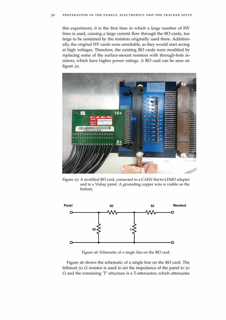
52 preparation of the panels , electronics and the tracker setup
this experiment, it is the first time in which a large number of HVlines is used, causing a large current flow through the RO cards, toolarge to be sustained by the resistors originally used there. Addition-ally, the original HV cards were unreliable, as they would start arcingat high voltages. Therefore, the existing RO cards were modified byreplacing some of the surface-mount resistors with through-hole re-sistors, which have higher power ratings. A RO card can be seen onfigure 25.
Figure 25: A modified RO card, connected to a CAEN flat-to-LEMO adapterand to a Vishay panel. A grounding copper wire is visible on thebottom.
Figure 26: Schematic of a single line on the RO card.
Figure 26 shows the schematic of a single line on the RO card. Theleftmost 50 ⌦ resistor is used to set the impedance of the panel to 50
⌦ and the remaining ’T’ structure is a T-attenuator, which attenuates

5.4 determination of operating voltage 53
the signal by 40 db, assuming the impedance is 50 ⌦ at the readout(right) side.
The HV cards were remade (figure 24). Their schematic design isdemonstrated by the wiring on the card.
The RO card flat output connector was connected to the DAQ sys-tem through a flat-to-LEMO adapter. Two (self made) of the fouradapters (figure 27) did not have a ground plane, as opposed to the
Figure 27: A self made flat-to-LEMO adapter. Note that there is no groundplane on the PCB.
CAEN adapters, so their resulting signals were slightly noisier, ascan be seen in the results section on figure 48. Panels C and E areconnected through the self made adapters, while B and H throughthe CAEN ones.
5.4 determination of operating voltage
It was observed that the rate of the panels increased with the ap-plied HV, starting from some minimal value below which the paneldid not produce pulses, as can be seen on a voltage scan on figure28. To generate this plot, starting from some minimal value, the HVsupply to the panel was increased by constant increments with anuncollimated �- source placed on four monitored readout lines. Thepulse rate was determined using a NIM counter module. The sameprocedure was done with the source removed, to determine the back-ground rate. Both the signal and the background pulse rates increasewith voltage.
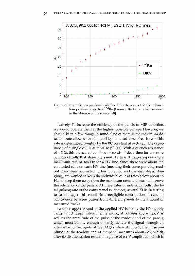
54 preparation of the panels , electronics and the tracker setup
Figure 28: Example of a previously obtained hit rate versus HV of combinedfour pixels exposed to a 106Ru � source. Background is measuredin the absence of the source [18].
Naively, To increase the efficiency of the panels to MIP detection,we would operate them at the highest possible voltage. However, weshould keep a few things in mind. One of them is the maximum de-tection rate allowed for the panel by the dead time of each cell. Thisrate is determined roughly by the RC constant of each cell. The capac-itance of a single cell is at most 10 pF [22]. With a quench resistanceof 1 G⌦, this gives a value of 0.01 seconds of dead time for an entirecolumn of cells that share the same HV line. This corresponds to amaximum rate of 100 Hz for a HV line. Since there were about tenconnected cells on each HV line (meaning their corresponding read-out lines were connected to low potential and the rest stayed dan-gling), we wanted to keep the individual cells at rates below about 10
Hz, to keep them away from the maximum rates and thus to improvethe efficiency of the panels. At these rates of individual cells, the to-tal pulsing rate of the entire panel is, at most, several KHz. Referringto section 4.3.1, this results in a negligible contribution of randomcoincidence between pulses from different panels to the amount ofmeasured tracks.
Another upper bound to the applied HV is set by the HV supplycards, which begin intermittently arcing at voltages above 1300V aswell as the amplitude of the pulse at the readout end of the panels,which must be low enough to safely deliver the signal through anattenuator to the inputs of the DAQ system. At 1300V, the pulse am-plitude at the readout end of the panel measures about 80V, which,after 60 db attenuation results in a pulse of 0.1 V amplitude, which is

5.5 tracker setup 55
acceptable by the DAQ. At 1300V the rate of each cell is well below 10
Hz. We therefore settle for a HV supply value of 1300V for all panelsin the tracker.
5.5 tracker setup
Figure 29: The tray holder built to hold the panel trays.
As a final step, the panels were connected to HV and RO cards andaligned on top of each other using two different methods. One, whichwas not successful, is discussed briefly in section 6.2 and shown onfigure 34 and the other one, successfully used, involves a custom-made tray holder shown on figure 29. Figure 30 shows a completesetup of the tray with four panels. The black plastic tray holdingstrips were manually aligned to be parallel with each other using amicrometer resulting in an estimated position uncertainty of up to± 1 mm. With the trays having a length of 65 cm and width of 39
cm, the maximum tilt (angle between the normal to the panel andthe vertical) resulting from those uncertainties is 0.3�. The verticaldistance between the holding strips was adjusted so that the verticaldistance between the center points of the gas gaps of two adjacentpanels is 37 mm. This was the lowest possible distance, due to thesize of the blue gas valves visible on figure 30. The uncertainty in thedistance is roughly estimated to be ± 2 mm (5%).

56 preparation of the panels , electronics and the tracker setup
Figure 30: A complete tracker setup with four trays. The fifth, inverted trayon the bottom holds a scintillator pad and another pad can beseen on top. Compare this to figure 38.
5.6 terminology
From now on, a few terms will be used to refer to various events andconfigurations of the experimental setup.
• Primary pulse - if an ionizing particle that passes through a PPScreates ion pairs inside a small volume in or near one of the ac-tive cells of the PPS, causing a discharge in that cell, the voltagepulse coming from that cell is called the primary pulse. Anypulse coming in a window of up to a microsecond after theprimary pulse from any one of the lines is considered to be asecondary pulse caused by unwanted physical phenomena inthe gas. In almost all acquisition events each panel had eitherzero or one primary pulse.
• Panel hit - a primary pulse from a panel which coincides withthe trigger. Whenever a trigger is generated, a snapshot is ac-quired of the outputs of all readout lines. If a panel has a pri-mary pulse withing that snapshot, we report a panel hit.
• Normal tracker setup - the tracker setup seen on figure 30 anddescribed schematically on the left side of figure 38, where fourpanels, with eight lines monitored on each are connected to aDAQ system and two scintillators, one above and one below the

5.6 terminology 57
stack of panels, so that the instrumented area of the panels andthe scintillators overlap.


6D A Q U S I N G T I M E M U LT I P L E X I N G
We tried two different approaches of DAQ system implementationsfor the tracker. The second approach will be described in the nextchapter. The first, failed approach was to use basic available equip-ment to make a "quick and dirty" solution, not involving any heavysoftware development. This chapter will briefly describe this attemptand present the first 2-point "track" observed.
6.1 daq equipment
We have used a set of NIM discriminators, logical and linear fan-infan-outs, NIM to ECL converters, timers and coincidence modulesalong with an Agilent MSO-X 4054A scope with four analog and 16
digital ECL logic inputs. In addition, we have utilized two NIM crates,LEMO cables and connectors.
6.2 implementation
Originally, we planned to do a 5-panel tracker with 16 lines moni-tored on each panel. The way to connect all panels to the scope wasto implement time-multiplexing of the panels, where all lines of panelk are delayed by an interval k�t, where �t is some constant time in-terval that is long enough to tell two signals apart. This way, ideally,a track would present itself as several digital pulses inside an acquisi-tion window, separated by intervals which are multiples of �t. Apartfrom connecting the lines of all panels to the digital scope inputs, weneeded to implement a triggering mechanism, to be fed into one ofthe analog inputs of the scope and used as the trigger for the DAQ.This triggering mechanism must be a fairly elaborate one, since wemust store the most interesting events, as the internal storage of thescope is limited to just 1000 acquisitions.
A simple implementation of DAQ and trigger for two panels andtwo connected lines is shown in figure 31. The lines coming out ofpanel B are delayed by �t with respect to the lines coming frompanel A. A resulting trigger and line signal is shown in figure 32. Insetups of this kind, we need to make sure that we set the discrimina-tor thresholds and widths of the resulting NIM logic signals from thevarious modules involved so that everything is synchronized prop-erly before the signals reach the coincidence modules. Note that inthe figure 31 setup, a trigger signal is generated when either panel Aor panel B has a signal.
59

60 daq using time multiplexing
Figure 31: The initial idea of DAQ and trigger implementation using NIMmodules.
Figure 32: Shown on the left are raw signals from the two scintillators andfrom lines 1,2 of panels A,B, respectively. On the right are theexpected inputs into the analog channel (trigger) and two digitalchannels of the scope, after being processed by the setup shownin figure 31. Also shown is the acquisition window of the scope,the width of which is configurable.
Ideally, this should work, but the panels we have, being first proto-types, are far from ideal and present a large amount of after-pulsingwhen several HV lines are connected, as shown, for example, on fig-ure 33, as well as inducing strong electromagnetic noise in the digitalinputs of the scope.
In order to solve the noise issue, a lot of shielding was successfullyused to eliminate the noise. At first, we tried to shield the cables, butthat did not produce any results. All cables used, besides the ones

6.2 implementation 61
Figure 33: Example of after-pulsing on one line of a panel recently filledwith 99% argon and 1% CF4 gas, connected to 930V with 3 HVlines. The first pulse is the primary, most likely caused by anelectron emitted by a 106Ru source and the one following it is anafter-pulse.
connected to the digital inputs of the scope, are coaxial cables whichare already well-shielded and the shielding is well-grounded. Oncethat didn’t work, we wrapped the trays holding the panels entirelywith aluminum foil and grounded them to the metal workbench. Wemade sure that the workbench, all ground connections and shieldingwere connected to common ground and firmly connected to the metalcasing of the power supply, with a thick copper braid. This eliminatedthe noise entirely and we could see clear digital signals on the scope.
The noise from a panel was eliminated only when the entire trayholding the panel was wrapped in aluminum foil. This preventedus from using the convenient tray holder, shown on figure 29 thatwas especially constructed to hold the trays so that they are almostperfectly aligned with each other. This required a new way of stackingand aligning the trays, which we did by using pieces of the rim ofthe tray, wrapped in aluminum foil for conductance and grounding,placed on the rims of the bottom tray, to support the upper tray, asshown on figure 34.
In order to solve the after-pulsing issue, we needed to make theimplementation even more complex, introducing generation of VETOsignals for the discriminators. Since each line could have after-pulses,we now needed to discriminate each line of each panel and when, forexample, panel A had a primary pulse on one of it’s lines, generate aVETO signal for all discriminators to which the lines of panel A are
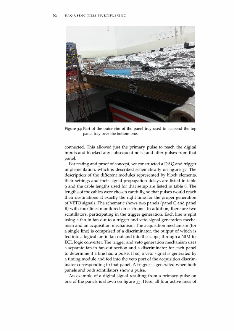
62 daq using time multiplexing
Figure 34: Part of the outer rim of the panel tray used to suspend the toppanel tray over the bottom one.
connected. This allowed just the primary pulse to reach the digitalinputs and blocked any subsequent noise and after-pulses from thatpanel.
For testing and proof of concept, we constructed a DAQ and triggerimplementation, which is described schematically on figure 37. Thedescription of the different modules represented by block elements,their settings and their signal propagation delays are listed in table9 and the cable lengths used for that setup are listed in table 8. Thelengths of the cables were chosen carefully, so that pulses would reachtheir destinations at exactly the right time for the proper generationof VETO signals. The schematic shows two panels (panel C and panelB) with four lines monitored on each one. In addition, there are twoscintillators, participating in the trigger generation. Each line is splitusing a fan-in fan-out to a trigger and veto signal generation mecha-nism and an acquisition mechanism. The acquisition mechanism (fora single line) is comprised of a discriminator, the output of which isfed into a logical fan-in fan-out and into the scope, through a NIM-to-ECL logic converter. The trigger and veto generation mechanism usesa separate fan-in fan-out section and a discriminator for each panelto determine if a line had a pulse. If so, a veto signal is generated bya timing module and fed into the veto port of the acquisition discrim-inator corresponding to that panel. A trigger is generated when bothpanels and both scintillators show a pulse.
An example of a digital signal resulting from a primary pulse onone of the panels is shown on figure 35. Here, all four active lines of
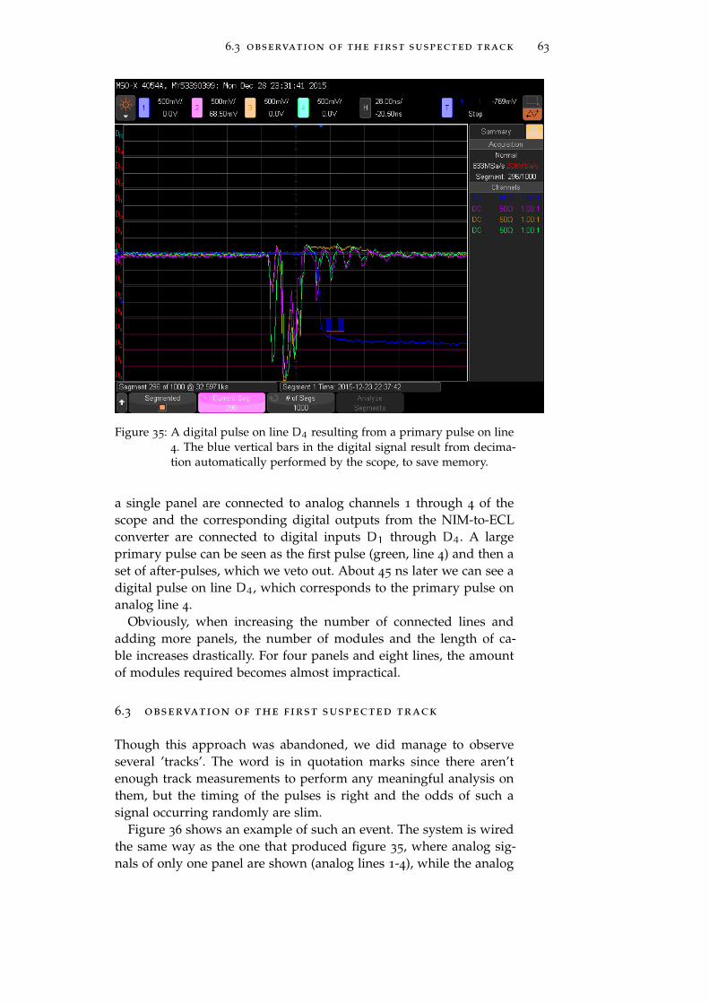
6.3 observation of the first suspected track 63
Figure 35: A digital pulse on line D4 resulting from a primary pulse on line4. The blue vertical bars in the digital signal result from decima-tion automatically performed by the scope, to save memory.
a single panel are connected to analog channels 1 through 4 of thescope and the corresponding digital outputs from the NIM-to-ECLconverter are connected to digital inputs D1 through D4. A largeprimary pulse can be seen as the first pulse (green, line 4) and then aset of after-pulses, which we veto out. About 45 ns later we can see adigital pulse on line D4, which corresponds to the primary pulse onanalog line 4.
Obviously, when increasing the number of connected lines andadding more panels, the number of modules and the length of ca-ble increases drastically. For four panels and eight lines, the amountof modules required becomes almost impractical.
6.3 observation of the first suspected track
Though this approach was abandoned, we did manage to observeseveral ’tracks’. The word is in quotation marks since there aren’tenough track measurements to perform any meaningful analysis onthem, but the timing of the pulses is right and the odds of such asignal occurring randomly are slim.
Figure 36 shows an example of such an event. The system is wiredthe same way as the one that produced figure 35, where analog sig-nals of only one panel are shown (analog lines 1-4), while the analog

64 daq using time multiplexing
signals from the other panel are not monitored. Here a primary sig-
Figure 36: A good track candidate.
nal on analog line 2 (purple) causes a digital signal to be generatedon line D2 roughly 45 ns later. A bunch of digital signals then fol-low, resulting from pulses coming from the seconds panel, with aleading digital signal also on line D2. The reason for the bunchingof the digital signals coming from the other panel is that we usedslightly different discriminators for the two panels - 4608B and 4608C(see figure 37). The discriminator used on the panel producing thebunched signals (4608C) cannot veto all the noise that comes afterthe initial primary pulse as fast as 4608B can, resulting in trailing dig-ital noise. Nevertheless, it was observed consistently that the leadingdigital pulse is located on a digital line corresponding to the analogline that produces the primary pulse. The interval between the startof the digital signal resulting from the first panel and the one result-ing from the second one is close to 26 ns, which is the actual planneddelay between the digital signals from the two panels, as can be ver-ified by the length of the L12 cable in table 8. Figure 36 is thereforean example of a good candidate for a vertical 2-point track. I will notelaborate any further on the results from this acquisition method.

6.3 observation of the first suspected track 65
Figure 37: Schematic of acquisition and trigger implementation for 2 panels,with 4 lines connected on each.
Table 8: List of cable lengths on figure 37. The length is measured by thetime it takes for a signal to propagate down the cable
Label Total Length (ns)L1, L10 2
L2, L11 20
L12 26
L3, L6, L13, L7, L19, L14, L8, L20, L15,L21, L22, L23, L9, L16, L17, L18
1
L4, L24, L25 10
L5 (digital probe cable) ~10

66 daq using time multiplexing
Table 9: List of the modules on figure 37, their descriptions, settings and thetime delays they introduce to the signal
Name Description Settings Max. delay428F Fan-in fan-out,
linearSet to “Normal” 6 ns
4608C Discriminator Threshold:lowest (-1.08V)width:narrowest
18 ns
4608B Discriminator Threshold :lowest (-9.1V) ,width:narrowest
18 ns
620CL Discriminator Threshold: -5V,Section A set to20 ns, B,C,D,Eset to widest (40
ns)
8 ns
622 Coincidencemodule
Width of allsections set to 1
µs
9.5 ns
429A Fan-in fan-out,logic
Main switch setto 4⇥4
6.5 ns
4616 NIM to ECLconverter
Connected sothat line 1
corresponds toD1 on scope,line 2 to D2, etc.
6.5 ns
MSO-X-4054A Digitaloscilloscope
Digital lines on,triggered on line1, at -750 mV
Panel B Top panel At 1380V ~5 ns (fromdischarge)
Panel C Bottom panel At 1380V ~5 ns (fromdischarge)
Scintillators 2 scintillatorsplaced on top ofeach other overthe active areaof the stackedpanels
At 1950V ~5 ns (from amuon passingthrough)

7D A Q U S I N G A D I G I T I Z E R
After realizing that time multiplexing is not practical, we decided toutilize a VME-based 32 channel CAEN V1742 digitizer. The digitizerspecifications are listed in section A.3.7 and it is sufficient to simulta-neously read out eight channels of four panels, thus making a small4-panel tracker with just one digitizer board. The advantage of thosedigitizers is their scalability, allowing for expansion to a larger num-ber of panels with increasing numbers of lines, which makes themrelevant for future tracking measurements with the next generationsof PPS.
Another major advantage of the digitizer is significant simplifica-tion of the trigger mechanism. The trigger in the time-multiplexingscheme was restrictive, to compensate for the limited amount of in-ternal memory in the scope, so we wanted to record just the mostinteresting events. In the case of the digitizer, however, this is not re-quired, because the amount of data we can store is now limited by theamount of PC storage, which is in the terabytes. We can therefore bemuch less restrictive when designing the trigger. In fact, it is enoughto use a simple double coincidence of two scintillators and to recordthe signals on all of the lines whenever the trigger fires.
An additional advantage is the fact that the data is being fed inreal-time into a PC, which enables elaborate analysis and monitoringof the whole setup in real time, enabling online monitoring of thesystem.
7.1 digitizer-pc interface
The accumulation of digitized samples in the digitizer is at the rateof the triggering. Since the trigger rate in our case is of the order of afew Hz, a slow digitizer-PC interface is sufficient to read all acquireddata in real time. It is therefore sufficient to connect the digitizer tothe PC through the slower but easier-to-use USB port of the VMEbridge and not through the optic fiber connection.
7.2 digitizer-panel interface
The connection between the panels and the digitizer is schematicallydescribed on figure 38. Since the digitizer’s inputs accept signals ina voltage range limited to ±0.5 V, further attenuation is needed afterthe RO cards, as the pulse height in the RO card output can reach am-plitudes of 5 V, depending on the HV the panel is connected to. The
67

68 daq using a digitizer
attenuators we used attenuated the signal by a further 20 db, givinga total attenuation of 60 db (the RO card has on-board attenuation of40 db).
Figure 38: A diagram of the complete setup using four PPS devices, twoscintillators, a coincidence and a discriminator module, 32 20dbattenuators and the CAEN V1742 digitizer. The thick arrows rep-resent eight cables and the attenuator blocks represent an attenu-ator on each one of the eight cables.
7.3 trigger setup
The trigger is a simple double coincidence of two scintillators. Thesetup is shown on figure 38. The scintillators are each fed into a dis-criminator, then into a coincidence module set to AND and then intothe TRG_IN input of the digitizer. Since the TRG_IN input does notacquire the trigger signal and is used just to signal the digitizer to ac-quire data, we split the trigger signal into the TR0 low-latency triggerinput, which stores the trigger waveform along with the rest of thechannels for timing analysis.
7.4 acquisition and analysis software
In order to fully utilize the power of the digitizer we need to writeproprietary software to read and analyze data from it. Though thereare some sample applications downloadable from CAEN’s website,they need to be heavily modified to suit our needs. The software foracquisition and analysis was written in C++ integrated within theROOT framework. The complete source code can be browsed anddownloaded from
https://github.com/davereikher/pps-daq

7.4 acquisition and analysis software 69
7.4.1 Architecture
The acquisition software is based on the CAENDigitizer library [26],which implements all the low-level details of communicating withthe digitizer through VME and provides a convenient interface to allof it’s required functionality. This library is not restricted to a singledigitizer model and can be used on any digitizer manufactured byCAEN.
The software was designed to be an analysis ’toolbox’, with a setof three executables:
• Acquisition - for acquisition, real-time analysis, monitoring andstorage of the acquired data into a ROOT file,
• Analysis - for offline analysis of the data in the ROOT file,
• Step - for looking at the acquired data event by event ("stepping"through them), to be used mainly for debugging and findinganomalies in individual events.
The acquisition and analysis tools perform the same operations onthe acquired data. There are two differences between them. The firstone is the delivery method of the data. In the acquisition tool thedata is being delivered by the digitizer, while in the analysis tool, thedata is being read from a ROOT file. The second difference is thefact that in the acquisition tool the data is processed in a separateexecution thread to avoid pileup of data in the thread performing theacquisition.
The analysis and acquisition tools are comprised of a set of analysisand monitoring modules, where each module is responsible for analyz-ing and monitoring a specific aspect of the experiment. For example,there is a track monitoring module, which is responsible for analyz-ing any potential tracks (hits on more than one panel in a single ac-quisition event), a degradation monitoring module, which monitorsthe activity of each panel and helps see if a panel degrades with timeand a few more, which are listed in the appropriate subsection below.
7.4.2 Primary Pulse Tagging
The most important part of the software toolbox (specifically of the ac-quisition and analysis tools) is the ability to read a set of samples fromthe digitizer, analyze them and decide whether there was a pulse com-ing from a primary discharge on one of the panels connected to thedigitizer. Very generally, each channel corresponds to a single line ona single panel. The channels are grouped together into panels in thesoftware (this grouping is provided in an external configuration filedescribed in section 7.4.8). At each acquisition event (once a trigger is

70 daq using a digitizer
generated), the digitizer interfacing code reads the data from the digi-tizer, passing it to the analysis code, which detects whether there wasa primary signal in any of the panels. The timing information and theresult of this analysis are sent to the various analysis and monitoringmodules which generate plots and activity logs (track characteristics,triggering rate, panel activity and so on).
A discharge signal coming from a panel is characterized by a lead-ing large negative pulse (the primary pulse) on a single line of thepanel, mixed with smaller, simultaneous induced pulses in the otherlines of the panel, followed by ringing and after-pulses on multiplelines. To find a primary pulse corresponding to a discharge signaland tag it as such, we need to find the channel corresponding to aline with the first pulse on the panel and make sure that this pulseis well-separated in time from the rest of the large pulses on thispanel and well separated in amplitude from the smaller simultane-ous pulses that are induced on the other lines. We must also makesure that no significant voltage fluctuation precedes it. The process isrealized using a set of configurable thresholds, listed in table 10 andexplained in the following sections.
Before looking for the primary pulse, it is necessary to fix differ-ences in per-channel DC offsets due to small differences in the resis-tances used in the attenuators connected to each channel. This is cor-rected in software, by bringing the zero of each waveform to 0 volts.This is done by working with several thresholds, IDLE_LINE_DURATION,which defines a duration of a flat line section in the waveform to cal-culate the DC offset from and IDLE_FLUCTUATION_AMPLITUDE, whichdefines the maximal amplitude of fluctuations below which a line isconsidered flat. A waveform before and after normalization is shownon figure 39. See section 7.4.2.1 for more details.
(a) (b)
Figure 39: The same signal, showing eight lines on a single panel beforebringing the waveforms from different channels to a commonzero voltage (a) and after (b).
In order to tag a pulse as a primary one, the following requirementsmust hold for it:
• it must come before any significant fluctuation in voltage takesplace (because it comes from the initial discharge),

7.4 acquisition and analysis software 71
• it must have a sufficient amplitude,
• it must appear enough time before any after-pulse.
For that, we define another three thresholds. PULSE_THRESHOLD, whichis a voltage threshold that defines the threshold of a primary pulse (ifa sample is found exceeding this threshold, the waveform potentiallycontains a primary pulse), EGDE_THRESHOLD, which is a voltage thresh-old that, similarly to a discriminator threshold, defines the voltagethat, once exceeded, marks the start of a primary pulse (location ofleading edge) and MIN_EDGE_SEPARATION, which is a time thresholdthat defines the minimum separation between the leading edge ofthe first pulse in a waveform and the one following it, so that the firstone could be considered as a primary pulse. There are a few moreauxiliary thresholds which are explained by going over the generaloverview of the source code in the next three sections.
7.4.2.1 Code Overview - Finding the DC Offset for Waveform Normaliza-tion
In order to normalize the waveforms, as discussed above, we need tofind the DC offset of each channel and then add to all samples in thatchannel the difference between the actual zero voltage and this DCoffset. The steps to finding the DC offset are:
• Divide a single channel waveform into sections of lengthIDLE_LINE_DURATION.
• For each section, make sure the section is flat, by verifying thatnone of the samples in it exceeds IDLE_FLUCTUATION_AMPLITUDE.
• Once a flat section is found, calculate the average value of thesamples in it and return this value.
• if a flat section is not found, this channel will not be adjusted(this almost never happens, since the sections are small and theacquisition window is wider than a typical signal, so there arealways flat sections).
7.4.2.2 Code Overview - Primary Pulse Tagging
The steps involved in tagging a primary pulse on a panel is as follows(this is done for each panel separately):
• Generate a list of pairs of the leading edge location and pulseminimum values (see section 7.4.2.3), where each pair corre-sponds to a single channel (a single line). The index in this listis the line number and the value is a pair (leading edge location,pulse minimum) for that line.

72 daq using a digitizer
• Look for the line with the earliest value of the leading edgelocation (call it line a).
• Look for the line with the next-to-earliest value of the leadingedge location (call it line b).
• If the distance between the leading edge location of line b andthat of line a is greater than MIN_EDGE_SEPARATION, then line a
has the primary pulse of this panel in this particular acquisitionevent and the pulse minimum is given by the pulse minimumvalue in the line’s corresponding pair.
• If the above difference is smaller than MIN_EDGE_SEPARATION,generate a list of lines for which the first pulse’s leading edgelocation is situated within a window of width MAX_EDGE_JITTER
after the earliest leading edge.
• In the above list, find the line with the lowest minimum ofthe pulse. This line and all lines in this list, the minima of thefirst pulses of which are situated within a window of heightMAX_AMPLITUDE_JITTER above that lowest minimum, are consid-ered as potentially having a primary pulse (there is an ambigu-ity in which line had the primary pulse if there are more thanone).
7.4.2.3 Code Overview - Generation of the List of the Leading Edge andPulse Minimum Pairs
This is an expansion of the first bullet in section 7.4.2.2, in which alist of leading edge locations and pulse minima needs to be generated.The steps for generating this list are as follows (this is done for eachline):
• Look for the first fluctuation in the voltage on the line by look-ing for a sample that exceeds PULSE_START_THRESHOLD.
• If such a sample is not found, this line doesn’t have a pulse anda corresponding reserved value is generated for the resultingpair to let the rest of the analysis code know that there is nopulse here.
• If such a sample is found, look for a later sample that exceedsPULSE_THRESHOLD within a window of width EXPECTED_PULSE_WIDTH
from the time of the initial sample.
• If such a sample is not found, this line doesn’t have a pulse anda corresponding reserved value is generated for the resultingpair.

7.4 acquisition and analysis software 73
• If such a sample is found, look for the first occurrence of a sam-ple that exceeds EDGE_THRESHOLD and find the lowest samplewithin a window of width EXPECTED_PULSE_WIDTH starting fromthat moment. Those two samples will constitute the pair corre-sponding to this line.
7.4.3 Analysis and Monitoring Modules
As mentioned earlier, the results of the primary pulse detection andtiming information are sent to various analysis and monitoring mod-ules which help visualize and log important information about the ex-periment run. It’s worth mentioning that each module can be turnedon and off by the user to avoid cluttering the screen with plots. Belowis the complete list of those modules.
7.4.3.1 Trigger Timing Monitor
Monitors the timing of the trigger (double coincidence of the scintil-lators) and produces a plot that can be seen on figure 40. The top padof the plot is the distribution of the time intervals between triggersand the bottom pad is the rate of the trigger.
7.4.4 Panel Hit Monitor
For each panel, this module monitors the number of panel hits and,for each panel, generates a plot of the number of hits versus line onthat panel (that way we can monitor the activity of each line) alongwith a second plot of the number of primary pulses detected on thatpanel per acquisition event as a function of time into the experimentrun. An example plot is shown on figure 46.
7.4.5 Panel Timing Monitor
Using the arrival time of the trigger signal and the arrival time ofthe primary pulse, this monitor generates two figures. The first oneis the timing distribution histogram (jitter of primary pulse arrivaltime after the leading edge of the trigger pulse) and the second oneis a figure with a similar histogram for each line. Those two figureshelp us see if the panel as a whole and the individual lines behave asexpected. An example is shown on figures 44 and 45.
7.4.6 Panel Degradation Monitor
Generates a figure for each panel, structured exactly as the one gen-erated by the trigger timing monitor (figure 40), where each entry isnow a panel hit. For an example, see figure 42.

74 daq using a digitizer
Table 10: A list of the most important parameters and their values in theconfiguration file.
Description Value
EDGE_THRESHOLD -0.11 VPULSE_THRESHOLD -0.13 VPULSE_START_THRESHOLD -0.02VIDLE_FLUCTUATION_AMPLITUDE 0.05 VIDLE_LINE_DURATION 5% of acq.
windowMIN_EDGE_SEPARATION 3 nsMAX_EDGE_JITTER 2 nsMAX_AMPLITUDE_JITTER 0.1 VEXPECTED_PULSE_WIDTH 3 nsTrigger pulse threshold (to detect leading edge oftrigger)
-0.2V
7.4.7 Track Monitor
After the raw signals were analyzed, a list of (panel, line) pairs aregenerated on which a hit was detected. This list is fed to the trackmonitor module which detects whether at least two panels had a hitin a single event (meaning a track was detected), calculates the slopesof the tracks, if any, and generates angular distribution histograms.An example of an angular distribution generated by this module canbe seen on figure 54.
7.4.8 Configuration
The entire suite is configurable through an external file written inJSON format. The configuration file contains the values of all thresh-olds listed above, a list of panels and the channels-to-lines associationfor each panel, digitizer settings (resolution, sampling rate, voltagerange), various parameters for the different analysis modules and pa-rameters for the Monte Carlo simulation. The configurable thresholdsused in the analysis are listed in table 10. The values of the variousthresholds were chosen by careful manual analysis of a large numberof waveforms with the step tool.

Part III
A N A LY S I S O F R E S U LT S & C O N C L U S I O N S


8R E S U LT S
8.1 monitoring
Every time an experimental run was concluded, the quality of thedata was assessed by looking at the various monitoring plots thatwere produced during the run. The resulting plots are shown below.
8.1.1 Monitoring the Trigger Rate and Arrival Time Distribution
A two-pad plot with the histogram of the time intervals between sub-sequent triggers on the top and the rate of the trigger on the bottom,calculated every 10 minutes is plotted. An example of such a plot isshown on figure 40. The occurrence of the trigger is a Poisson process
Figure 40: Trigger timing monitor. The trigger rate exhibits natural expectedlevel of fluctuation.
so the time interval between two subsequent triggers is exponentiallydistributed. The rate should stay relatively constant in time. Figure 40
shows a healthy trigger, with exponentially distributed intervals anda constant rate. Figure 41 shows an example of the need to monitorthe trigger rate. At some point the trigger rate falls, traced to a faultyair conditioner in the lab.
77

78 results
Figure 41: Trigger timing monitor. At 340000 seconds the air conditioning inthe lab stopped working, which is clearly seen by the decrease inefficiency of the scintillators and reduction in the triggering rate.
8.1.2 Monitoring Panel Activity
The panels are monitored for degradation (mainly due to leakage ofair into the panel and degradation of the gas in the panel with time)by observing each panel’s hit rate. The Poisson nature of the hitsis also monitored by plotting the distribution of the time intervalsbetween two adjacent coincidences, just as in section 8.1.1, forminga plot shown on figure 42. This figure shows a healthy panel, whichdoes not degrade, as opposed to the example shown on figure 43,where a leaking panel was monitored.
Another way to see that a panel behaves normally is to plot a tim-ing histogram, which is the time interval between the arrival of theleading edge of the trigger and the arrival of the primary pulse fromthe panel in any acquired event where this panel has a primary pulse.What we expect to get is a plot similar to figure 11 - a distributionwith a main Gaussian part with a variance which characterizes thetiming resolution of the panel and a power tail towards the high endof the histogram which is caused by passage of muons through areaswith relatively low electric field, causing the resulting ionization elec-trons to drift a longer time towards the anode. Examples of healthytiming histograms are shown on figures 44 and 45.
A pulse from a panel is tagged as a primary pulse by the softwareafter it passes certain criteria defined by thresholds set in the external

8.1 monitoring 79
Figure 42: Example of a panel degradation monitor output for a healthypanel. The structure of the plot is identical to the one of figure 40.
Figure 43: Example of a panel degradation monitor output for a leakingpanel. Note the hit rate going down to zero.
configuration file. In order to qualitatively make sure that we have thecorrect values for them for a given experiment run we also monitorthe number of primary pulses tagged by the software, for each panel,

80 results
Figure 44: Timing histogram for a single healthy panel.
Figure 45: Timing histogram of all lines on a single panel.
at every event, as seen on the bottom pad of figure 46. Ideally, all pan-els should have either null or one primary pulse per event. However,occasionally two and more primary pulses per event are tagged. Thelower pad on figure 46 shows a healthy distribution of the amountof primary pulses. The solid horizontal line is a dense occurrenceof single primary pulses (a similar zero primary pulses line is notplotted), and the data points at higher vertical axis values representevents with a higher number of primary pulses. This distribution is’healthy’ because it results when the thresholds are carefully adjustedby looking at individual waveforms (see section 8.1.3). When an ex-

8.1 monitoring 81
Figure 46: Line activity for eight lines connected to channels 24 to 31 (top)and primary pulse tagging monitoring plot (bottom) for a singlepanel. The latter shows events as a function of time, with thenumber of tagged primary pulses plotted.
perimental run produces a distribution which significantly deviatesvisually from this healthy one, such as, for example, on figure 47, weneed to check the thresholds by analyzing the waveforms on all thelines associated with the problematic panel.
In addition, the monitoring checks for equal activity levels in all thelines of each panel. To do that, we look at an individual line and countthe number of panel hits coming from that line. The result is shownon the upper pad of figure 46. A healthy panel with the thresholdsset appropriately has all lines roughly equally active, as seen on thisfigure. A panel with unequally active lines is shown on figure 47. Toget to the bottom of the problem we need to analyze the waveformsof the channels corresponding to the problematic lines.
8.1.3 Monitoring and Analyzing Signal Waveforms
In order to determine the thresholds used to tag primary pulses andto troubleshoot the system, we need to inspect individual waveforms.Figure 48 shows waveforms for all 32 channels used, grouped intofour panels with eight lines on each (each line has a different color).Panel H has a primary pulse while the other panels exhibit fluctua-tions induced in their corresponding channels by RF noise from theprimary pulse of panel H. A waveform showing a pulse coming from

82 results
Figure 47: A plot similar to the one on figure 46, showing a non-uniformactivity of the lines and bad primary pulse tagging, which can beseen by noting that there is a large number of events with threeprimary pulses and some events with four and five.
Figure 48: An example of the display of waveforms that is generated by thestep tool used to examine waveforms of individual events. Eachpad corresponds to a single panel, with eight lines monitored oneach (marked by a different color). On the bottom right panel apulse is visible and the line on which the pulse appears is auto-matically tagged and highlighted by a thicker line.

8.2 analysis 83
a healthy single panel with eight lines is shown on figure 49. Thelarge square pulse is the trigger signal and the two horizontal linesmark the thresholds EDGE_THRESHOLD (top line) and PULSE_THRESHOLD
(see section 7.4.2). The line that is tagged by the pulse tagging algo-rithm as carrying the primary pulse is plotted using a thicker line.
Figure 49: An example of a primary pulse waveform coming from a singlepanel with eight lines monitored. The channel with the primarypulse is highlighted by a thicker line.
An example of a waveform resulting from a bad connection on oneof the lines is shown on figure 50. We can see that the line correspond-ing to channel 16 shows a repetitive pattern with a large amplitude,as opposed to the other lines.
Generally, the signals obtained from the panels are rather noisyand not optimal for a particle detector. In our experiment, howevertrailing noise after a primary pulse does not affect our measurementssince it lasts for a very short time (hundreds of nanoseconds) com-pared to the trigger rate, having no noticeable effect on subsequentsignals.
8.2 analysis
Our goal is to look for tracks, which present themselves as eventswith a primary pulse on several panels. In order to confidently saythat such events represent actual tracks that result from MIPs passingthrough the tracker, we need to rule out random coincidence betweenpulses of separate panels and any significant effect of RF noise gener-ated by either the PMTs of the scintillators or by any one of the panels.

84 results
Figure 50: An example of a panel with 15 instrumented lines and a badcontact on the flat-to-LEMO adapter, on channel 16, exhibiting anabnormally large voltage fluctuation.
Such noise could create correlated pulses in some of the tracker ele-ments (the PMTs or the panels) which could lead us to mistakenlyinterpret them as tracks (referred from here onward as ’fake tracks’,as opposed to ’true tracks’).
The total track detection rate averaged about 10
-4 Hz, which is atleast one order of magnitude higher than the worst-case scenario rateof tracks resulting from random coincidences of pulses in the panelswe calculated in section 4.3.1. We can therefore safely say that thecontribution of random coincidence to the track rate is negligible.
RF noise poses a more serious problem. One problem with hav-ing fake tracks in our tracker setup is the low rate of total (true +false) track detection (as mentioned earlier, 10
-4 Hz), due to the lowefficiency of the panels. We need to make measurements that willshow, with a high confidence level, that the fake track rate is signif-icantly lower than the total track rate. For that, we had to collect a

8.2 analysis 85
large data sample while limited by our low-efficiency panels and thelimited rate of cosmic muons. In the following sections, wheneverpossible, we rule out RF effects while for more difficult cases I showthat the contribution of fake tracks, if not completely negligible, isnot obviously significant and propose experiments that can be doneto entirely dismiss those effects.
8.2.1 Effects of Panels on Scintillators and Vice-Versa
In order to show that the contribution of the panels affecting the PMTsof the scintillators and vice-versa to the amount of true tracks is neg-ligible we use the setup described schematically on figure 51, where
Figure 51: A schematic of the experimental setup used to test effects of PMTson track detection rate.
the normal setup of the tracker is used, with the exception that thescintillators are moved so that the scintillator pads overlap each other,but do not overlap the stack of panels and that their PMTs are directlyunderneath and above the stack. This way, MIPs will not contributeto any registered ’tracks’ at all and all we should see is contributionof RF noise from the PMTs on the panels and vice versa as well as ran-dom, uncorrelated pulses from the panels. The setup collected datafor 250000 seconds (four days). The result was the detection of two2-point tracks in four days.
If a significant number of tracks was originating from RF noise, wewould get a track detection rate of 10-4 Hz in this setup, but we got arate of the order of 10-6 Hz. We can therefore rule out any significantcontribution to the fake track rate of the effect of the PMTs on thepanels. In fact, this low rate is consistent with the rate we calculatedat the end of section 4.3.1, resulting from random coincidence, so itmight not even be a result of RF noise.
8.2.2 Effect of Panels on Each Other
Another effect that must be ruled out is the effect of panels on eachother. If pulses in one panel electromagnetically induce pulses in an-

86 results
other panel, we will see fake tracks, caused by this correlation be-tween panels. This effect should also cause an increase in pulsingrates of an active panel surrounded by active panels, versus an ac-tive panel surrounded by inactive panels. This was tested by usingthe normal tracker setup, running a single panel with the three sur-rounding panels off for a while and then applying the usual HV tothe surrounding panels all at once, all the while measuring the hitrate of the single panel. The result is shown on figure 52. It can be
Figure 52: Hit rate (calculated every 1200 seconds) as a function of time of asingle panel surrounded by three panels (two on the bottom andone on top) before and after the surrounding panels are turnedon. The arrow marks the moment when they were turned on.
seen that there is no significant difference in rate before and after theactivation of the surrounding panels. However, we will show that thisis not enough.
To further quantify any effect of panels on each other, we can lookat two-point tracks only, since they form the majority of acquiredtracks. Looking at a very long interval of time T , the total numberof tracks N acquired by the tracker within T can be written as thesum N = Nt +Nf of the number of true tracks (Nt) and fake tracks(Nf), resulting from panels affecting each other. We need to showthat Nf ⌧ N to reject this effect. The number of true tracks can befurther decomposed into a sum of contributions, each coming from adifferent pair of panels:
Nt = N12 +N13 +N14 +N23 +N24 +N34, (15)
where the subscript of each term are the two panels contributing inthat term. If the effect of surrounding panels on a single panel (say,panel 2) is an increase of the number of hits of that panel by �N,then each term involving panel 2 in eq. (15) gets a contribution ofthe order of �N or smaller (for panels farther away, as EM effectsdiminish as 1/r2). The contribution of the number of fake tracks to N
is therefore of the order of �N. Therefore, Nf ⇠ O(�N) and, since weare interested in placing an upper bound on Nf, we need to find anupper bound on �N.

8.2 analysis 87
If we mark the number of panel hits within the interval T beforeturning on the surrounding panels by N1 and after - by N2, the moredata we take, the smaller the uncertainties in N1 and N2 will become.We need to get enough data, so that those uncertainties are of the or-der of the maximal �N we allow, so that we could tell that N1 and N2
do not differ from each other by more than �N. Nf, and therefore also�N should be at least one order of magnitude below the measured to-tal track detection rate (N/T ⇠ 10-4 Hz). Since N1/T ⇡ N2/T ⇠ 10-2
Hz, as can be seen on figure 52, the maximum value for �N is
�N/T ⇡ 10-5 Hz ⇡ 10-3N1/T ⇡ 10-3N2/T ,
or
�N ⇡ 10-3N1 ⇡ 10-3N2.
The uncertainty needs to be of the order of �N, and since N1 and N2
are Poisson variables, their uncertainties are just their square roots,so
pN1 ⇡ 10-3N1
and similarly for N2. This gives N1 ⇡ N2 ⇠ 106. This amount ofhits at a rate of 10-2 Hz (the hit rate of a single panel) will takeabout 3 years to acquire, so it’s not practical and we therefore cannotcompletely reject inter-panel RF effects with our current setup andthe natural rate of cosmic muons. In order to reject inter-panel effects,we will need to make the same measurement with a much higherluminosity MIP source, such as using a beam of muons.
8.2.3 2-Point Tracks
The experimentally measured distribution of the � angle (see section4.5) is given on figure 53 and a histogram representing it’s projectiononto the observation plane is shown on figure 54. This is the form ofthose histograms we would expect to get for straight MIP tracks pass-ing through the tracker, as explained in section 4.5.1. The distortionof the histograms (described in section 4.5.1), limits us from furtherprecise angular analysis of their shape.
We use the Monte Carlo simulation to plot a similar angular dis-tribution that would result if the hits on the panels were completelyrandom. The result is shown on figure 55. For each iteration of thesimulation, a random 0 or 1 value was generated for each panel inthe stack. If the value is 1 for a panel, a hit is generated on that panelon a line the number of which is randomly selected from a uniformdistribution. We note that qualitatively, figures 55 and 54 differ fromeach other in their structure. The histogram on figure 54 exhibits amore ’layered’ structure than the one on figure 55. We also performed

88 results
Figure 53: Two-dimensional histogram of angular distribution. The axes arethe angle � of the track (see section 4.5.1) and the distance be-tween points on the track.
Figure 54: One-dimensional histogram representing the angular distribu-tion of tracks as seen from the observation plane. 97% of thetracks here are 2-point tracks. Note the layered structure, ex-plained in section 4.5.1.
a Pearson’s �2 test to compare the two histograms, and the resultingp-value was practically zero, rejecting the hypothesis that the two his-tograms originate from the same distribution.

8.2 analysis 89
Figure 55: One-dimensional histogram representing the angular distribu-tion of ’tracks’ that would result from completely random hitson the panels.
8.2.4 3-Point Tracks
Following the discussion in section 4.5.2, we plot the Distributionof the �2 per NDF of the resulting 3 and 4-point tracks (figure 56).Even though the histogram includes 4-point tracks, there are only a
Figure 56: �2/NDF histogram of the 243 3 and 4-point tracks we acquiredin a period of roughly two months.
few of them, so we cannot perform any significant statistical analysis

90 results
on them. We can already see that the majority of tracks have a verylow value of �2, which means that the 3 points comprising them arecollinear (for �2 = 0, about 125 tracks) or nearly collinear. To rule outthe option that this histogram could result from completely randomhits on the panels, we assume a null hypothesis that the hits are com-pletely random and run a Monte Carlo simulation, similar to the onewe did for 2-point tracks, that results in the �2/NDF plot shown onfigure 57. Using the Chi2Test method of the TH1 class in ROOT, which
Figure 57: �2/NDF histogram of 3 and 4-point tracks generated by a MonteCarlo simulation where each hit on each panel is assumed tocome from a random line.
implements Pearson’s �2 test, a comparison of the two histograms infigures 56 and 57 was performed and yielded a �2 value which cor-responds to a p-value of practically 0 (much lower than 0.01), so wereject the null hypothesis.

9C O N C L U S I O N S
Plasma panel sensors is a promising technology of particle detectorsin the micropattern gaseous detector category. Previous research onprototypes of PPS devices had shown potentially high-end values ofcharacteristics such as spatial resolution, timing resolution and deadtime, characterizing detectors operating in the Geiger-Mueller regionand beyond. An additional advantage of PPS devices is the low man-ufacturing cost, resulting from overlap of the manufacturing processwith the one of commercial PDPs as well as the lack of need in cum-bersome and expensive gas re-circulation systems used in today’sgaseous detectors.
The work described here has shown that it is possible to use pro-totype PPS devices, which are no more than PDP panels filled witha different gas mixture, to perform tracking measurements of cos-mic muons. In the tracker experimental setup, contribution to trackmeasurement rate of RF noise between tracker elements was partiallyruled out and we still need to perform an additional experiment witha high intensity MIP source in order to dismiss this effect completely.Nevertheless, we could not find anything that contradicts the hypoth-esis that the measured tracks are caused by cosmic muons.
As a part of the tracker development, a software suite for DAQ,storage and monitoring as well as real-time and offline pulse andtracking analysis and a toy tracker Monte Carlo model were imple-mented. These tools can be used for DAQ and analysis as well as forthe construction of tracking devices with newer generations of PPS.
As a final note, the tracker constructed and described in this thesisis a two-dimensional one, consisting of 4 panels with one-dimensionalreadout from each panel. Development of two-dimensional readoutfrom newer generations of similar panels is currently underway.
91


Part IV
A P P E N D I X


AD ATA A C Q U I S I T I O N S Y S T E M
a.1 triggering and daq overview
The process of data acquisition is comprised of two main operations.One is the acquisition of electronic signals coming from a detectorand their storage along with some basic analysis, and the other is ageneration of a trigger, which, as it’s name implies is used to trig-ger the DAQ system to perform the acquisition. Trigger setups rangefrom simple double-scintillator coincidence triggers to elaborate multi-channel triggers that analyze signals in real time and use patternrecognition techniques to detect specific signal forms. In our case, asimple double-scintillator coincidence trigger is sufficient, where dataacquisition is triggered whenever pulses from two overlapping scin-tillators coincide, which occurs when a MIP passes through both.
a.1.1 Scintillator Trigger
The scintillator in use is a solid-state detector of ionizing radiation. Itis comprised of a block of scintillating medium, which, with a highefficiency, emits photons whenever an ionizing particle (e.g. a MIP)passes through it. These photons are collected at one end of the scin-tillating block by a photomultiplier tube (PMT), which is comprisedof an interface that emits electrons through the photoelectric effectwhenever a photon interacts with it’s surface and a volume housingseveral electrodes (dynodes) with an increasingly large high voltageapplied to each subsequent one. The electrons emitted from the inter-face are accelerated in the volume, multiplying their numbers withevery hit of a subsequent dynode through secondary emission, untila significant current pulse is registered at the PMT’s output. Due tothe acceleration of charges inside, PMTs are sometimes a source of RFnoise in experimental systems. We deal with that issue in section 8.2.
In theory, it is enough to use a single scintillator at the detectorentrance to detect an incoming MIP and to use the resulting pulse totrigger data acquisition. In practice, a pulse from a scintillator couldresult from a variety of other sources, such as low-energy electronsfrom radioactive decays and RF noise induced in the PMTs by ex-ternal sources. Therefore, to reduce false-positives, a coincidence be-tween two scintillators is used as a trigger instead.
95

96 data acquisition system
a.2 daq equipment standards
In order to read a signal from a detector and process it, we needsuitable electronic equipment. For highly specialized experiments it’snot out of the ordinary to construct proprietary equipment, but forour purposes we chose to use some ready-made modules based onthe NIM, VME and ECL standards.
a.2.1 NIM
The Nuclear Instrumentation Module (NIM) system is a mechani-cal and electrical standard used in experimental particle and nuclearphysics. It provides electronics cards (modules), each with a distinctfunctionality. Some examples are discriminators (modules that con-vert an analog signal to a digital one using a voltage threshold), fan-infan-out, pulse counting, coincidence between pulses and pulse timingmodules. See section A.3 for further details about each module used.The modules are placed in a housing called a NIM crate. Figure 58
shows a photograph of a NIM crate with various NIM modules. The
Figure 58: A NIM crate with NIM modules [27].
NIM digital signals, used, for example, in discriminator and coinci-dence units, use a 0 voltage as a logic 0 and a negative voltage aslogic 1. This specification makes the NIM standard more susceptibleto RF noise, since the logic levels are measured relative to ground,and any RF-induced noise will distort the signal (ground potential isnot significantly affected by RF noise).
a.2.2 ECL
Emitter Coupled Logic (ECL) is a newer logic standard, where thesignals are transferred on two wires, one carrying the signal and theother carrying a complementary signal. The logic level is then de-termined by looking at the difference between the two signals. This

A.2 daq equipment standards 97
is more resistant to RF noise, since it affects both wires similarly. Inorder to convert NIM logic signals to ECL logic and vice versa adedicated module is used. Comparison between the NIM and ECLstandards can be found in [28].
a.2.3 VME
A standard architecture commonly used by nuclear physics and par-ticle physics experiments as well as medical and industrial studiesis the the computer bus “VERSAmodule Eurocard” (VME) standard[29]. This is a high-speed, high-performance bus system with power-
Figure 59: A VME Crate with a bridge (left) and a 32-channel digitizer mod-ule. The modules are plugged into the sockets visible on the backof the crate, which are connected to the VME bus. Gold-platedMCX-type inputs are visible on the front panel of the digitizermodule as well as larger LEMO-type inputs.
ful interrupt management and multiprocessor capabilities. Similarlyto a NIM system, a VME system is comprised of a VME crate andVME modules. The strength of the VME system is that VME mod-ules are connected to a bus and can therefore communicate with eachother and perform elaborate signal processing. Additionally, manymodules are programmable and thus much more flexible in function-

98 data acquisition system
ality than NIM modules. This enables us to build multi-channel DAQsystems with relative ease.
A VME crate with VME modules usually contains a master modulecalled the VME bridge, through which the user can send commandsand receive data to any module on the VME bus. Figure 59 shows anexample of a VME crate with a bridge and a digitizer module in ourlab.
a.3 daq equipment
a.3.1 Discriminator Units
An important element in detector signal analysis is the discriminator.Its purpose is to transform a signal from its analog form to a digital’true or false’ form, depending on the logic it’s based on. For example,a typical NIM-logic unit has an input port and several output ports.The input port is fed with a signal and the output ports show a NIM-logic 1 signal whenever the input signal passes a threshold which canbe set through turning a knob or screw on the discriminator frontpanel. The width of the output NIM-logic signal can also be set in asimilar manner. Discriminator units are usually comprised of severalsections, where each section is a separate discriminator and they allshare a single VETO input. As long as a logic 1 is fed into this input,all sections are inactive and output a logic 0 signal on their outputs,regardless of the input.
a.3.2 Fan-In-Fan-Out Units
A NIM-logic fan-in fan-out unit has several input and several outputchannels. The purpose of the unit is to superimpose all the signals inits inputs and have the result sent to all outputs. The fan-in fan-outmakes sure that all impedances are matched and therefore there isminimal signal deformation. A fan-in fan-out can be linear or logical,where the former linearly adds all the inputs and the latter behavesas a logical OR module for NIM-logic inputs.
a.3.3 Coincidence Units
A NIM-logic coincidence has two input ports and several outputports. The unit takes two logic inputs and outputs the result of theirlogic AND or logic OR operation. The choice is done by a switch onthe front panel.

A.3 daq equipment 99
a.3.4 Timer Units
Sometimes it is necessary to generate a logic signal of a certain length,at a certain timing. This can be done with a variety of timing units. Forexample, a NIM-logic timing unit can have an input through whicha signal can trigger generation of a signal on the output, of a lengthset by a knob on the front panel and delayed by a time set by anotherknob.
a.3.5 NIM to ECL Converter
A NIM to ECL converter is used to convert between NIM-logic andECL-logic signals in our case, where the digital oscilloscope expectsECL-logic signals in its digital inputs while most modules at our dis-posal are NIM modules.
a.3.6 Digital Oscilloscope
The scope we were using is a multi-functional Agilent MSO-X 4054Ascope. The features listed here are only the ones that are important forour purposes. It has 4 analog input channels and 16 digital ECL logicinputs. The sampling rate of the scope is 2.5 GHz and it can store upto 1000 snapshots of all the channels, in its internal memory, within avery wide window (hundreds of microseconds). The acquisition trig-gering is done by setting a threshold on one of the channels (digital oranalog), that, once reached, will trigger digitization of the waveformson all channels and will store them in the internal memory. Acquisi-tion of signals can be done in two ways. One is single-shot acquisition,where the waveform is displayed on the screen as soon as triggeringoccurs and remains there until the next triggering. Such acquisitionresults in a high-resolution image and is good for analyzing a singleevent during operation of the monitored equipment. The second oneis an acquisition of a pre-set number of snapshots of all the channelsinto internal memory. There can be up to 1000 such snapshots, butcare must be taken, however, when setting the higher-end settings,since the waveform samples are decimated if we are using the mostmemory-demanding settings, namely acquisition of all channels, withallocation of enough space for a 1000 snapshots. Additional featuresare a built-in waveform generator that can be used for tests and stor-age of the data (after acquisition is over) on an external USB drive invarious formats.
a.3.7 Digitizer
Generally, a digitizer takes analog signals as inputs and stores them,in digital form, in its internal memory for readout whenever a trigger

100 data acquisition system
is generated. The digitizer at our disposal was a CAEN V1742 VME32-channel digitizer (figure 59). This digitizer has the following set offeatures [30]:
• 1, 2.5, or 5 GHz sampling rate (configurable).
• 12 bit resolution digitization.
• 32 MCX analog input channels, divided into 4 8-channel groups.
• Input voltage must be in the range ±0.5V, adjustable by a ±0.5Voffset.
• 1 LEMO NIM-logic trigger input acting as an overall trigger.
• MCX low-latency trigger inputs (trigger signal should be fedhere in order to be saved along with the channel waveforms, fore.g. timing analysis).
• Each channel has a 128 event deep, 1024 sample long memorybuffer (each sample is 12 bits). Those buffers are filled as thetrigger fires and are emptied as data is read from them.
• USB and optic fiber data readout options (through a VME bridge).
• It is straightforward to connect more digitizers to accommodatemore channels.
In order to communicate with the digitizer it is necessary to use a setof libraries by CAEN supporting their digitizers [26]. The digitizercan be connected to a PC trivially through USB or, by using an ad-ditional PCI card, through an optical link. The latter option enablesmuch higher data transfer rates, however, the readout speed require-ments for the application discussed in this work are low enough touse the USB interface.
a.4 impedance matching and termination
When a signal propagates along a cable with a certain impedance andreaches a load which has a different impedance, the energy transferto the load is not maximally efficient, as some of the signal energywill be reflected back, causing unwanted ringing effects, which willpresent themselves as a decaying sinusoidal fluctuation in voltageafter each signal.
In order to maximize energy transfer and avoid those unwantedeffects, we need to make sure that the inputs and outputs of all elec-tronic modules and all cables used have the same impedance. All ofthe modules and cables at our disposal have the same input and out-put impedance - a standard 50⌦. We must also make sure that allcables that are not connected on either side are terminated there, to

A.4 impedance matching and termination 101
prevent reflection, since an open end of a cable is equivalent to havinga load at the end of it with a very high impedance.
The issue of reflection, termination and cable impedance can bebetter understood by looking at a coaxial cable as a long capacitor. Attime t = 0 a current step I starts flowing into the cable and chargingit. I depends on the capacitance of the cable. Assuming the voltageis V , the impedance seen from the input, as long as the current isflowing, is R = V/I. This is the impedance of the cable. When thecurrent step reaches the opposite end of the cable, a reflection intothe cable will occur, unless there is a termination resistance equal toR at that end, between the signal wire and the shielding of the cable,effectively making the cable seem ’infinite’, as seen from the input [2].


B I B L I O G R A P H Y
[1] R. Ball et al. “First results with a microcavity plasma panel de-tector.” In: Nucl. Instrum. Meth. A784 (2015), pp. 56–59. doi: 10.1016/j.nima.2014.11.028. arXiv: 1407.6491 [physics.ins-det].
[2] G.F. Knoll. Radiation detection and measurement. Wiley, 1989. isbn:9780471815044. url: https://books.google.co.il/books?id=dyBRAAAAMAAJ.
[3] K. A. Olive et al. “Review of Particle Physics.” In: Chin. Phys.C38 (2014), p. 090001. doi: 10.1088/1674-1137/38/9/090001.
[4] Bruno Rossi. “Interpretation of Cosmic-Ray Phenomena.” In:Rev. Mod. Phys. 20 (3 July 1948), pp. 537–583. doi: 10.1103/RevModPhys.20.537. url: http://link.aps.org/doi/10.1103/RevModPhys.20.537.
[5] Atomic and Nuclear Properties of Materials. http://pdg.lbl.gov/2015/AtomicNuclearProperties/.
[6] D. Green. The Physics of Particle Detectors. Cambridge Mono-graphs on Particle Physics, Nuclear Physics and Cosmology.Cambridge University Press, 2000. isbn: 9780521662260. url:https://books.google.co.il/books?id=xjHgxkhHlK0C.
[7] Fabio Sauli. “Principles of operation of multiwire proportionaland drift chambers.” In: CERN, Geneva, 1975 - 1976. CERN.Geneva: CERN, 1977, 92 p. url: https://cds.cern.ch/record/117989.
[8] Konrad Kleinknecht. Detectors for particle radiation. Cambridge:Cambridge Univ. Press, 1986. isbn: 9780521358521. url: http://cdsweb.cern.ch/record/108093.
[9] Yiftah Silver and Erez Etzion. “Search for Physics beyond theStandard Model with the ATLAS detector and the developmentof radiation detectors.” Presented 26 May 2014. PhD thesis. TelAviv U., Oct. 2013. url: http://cds.cern.ch/record/1756960.
[10] T. Francke and V. Peskov. Micropattern Gaseous Detectors. 2004.eprint: arXiv:physics/0404035.
[11] J. M. Meek. “A Theory of Spark Discharge.” In: Phys. Rev. 57
(8 Apr. 1940), pp. 722–728. doi: 10.1103/PhysRev.57.722. url:http://link.aps.org/doi/10.1103/PhysRev.57.722.
[12] V. Peskov and P. Fonte. Research on discharges in micropattern andsmall gap gaseous detectors. 2009. eprint: arXiv:0911.0463.
[13] H. Raether. “Die Entwicklung der Elektronenlawine in den Funkenkanal.”In: Zeitschrift fur Physik 112 (July 1939), pp. 464–489. doi: 10.1007/BF01340229.
103

104 Bibliography
[14] Robert Ball, John W. Chapman, Erez Etzion, Peter S. Friedman,Daniel S. Levin, Meny Ben Moshe, Curtis Weaverdyck, and BingZhou. “Plasma Panel Detectors for MIP Detection for the SLHCand a Test Chamber Design.” In: Proceedings, 2009 IEEE NuclearScience Symposium and Medical Imaging Conference (NSS/MIC 2009):Orlando, Florida, October 25-31, 2009. 2009, pp. 1321–1327. doi:10.1109/NSSMIC.2009.5402346. arXiv: 1007.0486 [physics.ins-det].url: https://inspirehep.net/record/860485/files/arXiv:1007.0486.pdf.
[15] J P Boeuf. “Plasma display panels: physics, recent developmentsand key issues.” In: Journal of Physics D: Applied Physics 36.6(2003), R53. url: http://stacks.iop.org/0022-3727/36/i=6/a=201.
[16] APD-128G032 Plasma Display Module Datasheet. Vishay. 2008.
[17] R. Ball et al. “Development of a plasma panel radiation detec-tor.” In: Nucl. Instrum. Meth. A764 (2014), pp. 122–132. doi: 10.1016/j.nima.2014.07.028. arXiv: 1403.3454 [physics.ins-det].
[18] Peter Friedman et al. “Plasma panel-based radiation detectors.”In: J. Soc. Info. Display 21 (2013), pp. 46–54. doi: 10.1002/jsid.151. arXiv: 1305.2277 [physics.ins-det].
[19] Peter S. Friedman et al. “Plasma Panel Sensors for Particle andBeam Detection.” In: Proceedings, 2012 IEEE Nuclear Science Sym-posium and Medical Imaging Conference (NSS/MIC 2012): Anaheim,California, USA, October 29-November 3, 2012. 2012, pp. 1775–1780. doi: 10.1109/NSSMIC.2012.6551416. arXiv: 1211.5399[physics.ins-det]. url: https://inspirehep.net/record/1203752/files/arXiv:1211.5399.pdf.
[20] Peter S. Friedman et al. “The Detection of Ionizing Radiation byPlasma Panel Sensors: Cosmic Muons, Ion Beams and CancerTherapy.” In: (2012). arXiv: 1204.0677 [physics.ins-det].
[21] D. S. Levin et al. “Development of a plasma panel muon de-tector.” In: Nucl. Instrum. Meth. A652 (2011), pp. 315–318. doi:10.1016/j.nima.2010.07.076.
[22] Yiftah Silver et al. “Development of a plasma panel radiationdetector: recent progress and key issues.” In: Proceedings, 2011IEEE Nuclear Science Symposium and Medical Imaging Conference(NSS/MIC 2011): Valencia, Spain, October 23-29, 2011. 2011, pp. 1881–1885. doi: 10.1109/NSSMIC.2011.6154379. arXiv: 1205.6829[physics.ins-det]. url: https://inspirehep.net/record/1116689/files/arXiv:1205.6829.pdf.
[23] Peter S. Friedman et al. “Large-Area Plasma-Panel RadiationDetectors for Nuclear Medicine Imaging to Homeland Securityand the Super Large Hadron Collider.” In: 48th SID InternationalSymposium, Seminar, and Exhibition 2010 Seattle, Wash., USA, May

Bibliography 105
23-28, 2010. 2010. arXiv: 1007.0487 [physics.ins-det]. url:https://inspirehep.net/record/860484/files/arXiv:1007.
0487.pdf.
[24] Robert Ball et al. “Progress in the development of a PlasmaPanel Detector.” In: Proceedings, 2010 IEEE Nuclear Science Sym-posium and Medical Imaging Conference (NSS/MIC 2010): Knoxville,Tennessee, October 30-November 6, 2010. 2010, pp. 1536–1539. doi:10.1109/NSSMIC.2010.5874033. arXiv: 1101.0045 [physics.ins-det].url: https://inspirehep.net/record/882991/files/arXiv:1101.0045.pdf.
[25] George Casella, Christian P. Robert, and Martin T. Wells. “Gen-eralized Accept-Reject sampling schemes.” In: A Festschrift forHerman Rubin. Ed. by Anirban DasGupta. Vol. Volume 45. Lec-ture Notes–Monograph Series. Beachwood, Ohio, USA: Insti-tute of Mathematical Statistics, 2004, pp. 342–347. doi: 10.1214/lnms/1196285403. url: http://dx.doi.org/10.1214/lnms/1196285403.
[26] UM1935 CAENDigitizer Library - Library of Functions for CAENDigitizers High Level Management. CAEN. 2016.
[27] Fermilab Equipment Catalog. http://prep.fnal.gov/Catalog.php.
[28] Electronics Standards and Definitions. http://www.ortec-online.com/download/electronics-standards-definitions.pdf. Or-tec.
[29] Introduction to VME / VXI / VXS Standards. http://file.wiener-d.com/documentation/General/WIENER_VME_VXI_VXS_introduction_
1.0.pdf. Wiener.
[30] Mod.V1742 32+2 Ch. 12bit 5GS/s Switched-Capacitor Digitizer. CAEN.2012.

�⇥⇤⌅⇧�⇥⇤⌅⇧�⌃ �⇤⇧ ⌦⇥⌃↵ �⇤⇤⌅⌦�⇥⌃ �⇤��✏ �⇣ ↵⇤⌦⇥✏⌘✓� �⇤ ⇤⇤⇣↵ ↵⌅⇤⌦✓ ⇤��✏ �↵ ↵⌃◆� ⇤�⌅ ✏⇥�⌃ �⇤��✏���⇥⇧⌃ ↵⌃◆� ⇤�⌅ ✏⇥�⌃ �⇤��✏ �⇣ ↵⇤✏⇥�⇥⌅ ⌘↵ .⇥⌃⌫⇠ ⇤⌅⇧ ⇤��✏ ↵⇥⇥↵⌃ ⇡↵⌃ �⇢� � ⌦⇣� ,�⇥⌦⇤⇠◆
�⇤⇤⌦⇢�⌃ ↵⌃◆� ⇤ �⌃ �⇠ ↵ �⇠ ↵⇣⇠⌅⇣ ⌦✓⇢⌃↵ �� �⌃ �⌃ ⇥◆ ↵�⇥⇧⇠ .↵⌃◆� ⇤ �⌃ �⇣ ⇥◆ �⇠⇤�⇥��⌃ ⌦◆⇢⇣⌃↵ ⌦⇤⇣ ⌃ �⇣ ↵⇤⌅⇧↵ �� �⇤⌘⌦� ⌦��⌃⇥ �"⌅↵ �⇤��✏↵ �⇣ �⇥⇤⌘-�⇥⇧�� ⇥⌦⌃⇥↵⇣
⌃ ⇧ ⌦⇥⌃↵ ("⌦✓�⌦⌘" ⇡�↵�) �⇤�⌃⌃ ⇤⌅⇣⇧ �⇤✓⇤✓�⇢4��⇤⌦✓ �⇠⌫⇧�⌃ ⌦⇣� �⇤��✏↵ �⇣ �⇥⇧ ⇣ .�⇤⌃�⇥✓ ↵⌅⇤⌦✓⇧ �⌦⇥✓⌃⇣ �⇤⌅⇥�⇥⇤⌃ ⇤�⇥��⌃ �⇣ ⇥�⇥⇠⌫⌃�⇧ ⌦⇥◆⇢⇣⇥ ⇤��✏ � ⌃ �⇤�⌃⌃!�⇢ �⇤�⌅✏⇤�
-⌃ �⇤⇧ ⌦⇥⌃↵ �⇤�⇥��⌃ �⇣ ↵�⇥�✏ �⇥⌃ 2-⌃ �⇤⇧ ⌦⇥⌃↵ �⇤�⇥��⌃ ⇥�⌫⌃⌅ ⇡ -⇥⌃ ⇥ ⇥↵⇥◆ �⇥�⇥✓⌅ 3-⇥ 4�⇣ �⇤�⇤⇥◆↵ �⇥✏��↵↵ �⇠ ⇥⇣⇠⌅ (�⇤⇤⌘�⇤⌘⌘� ↵�⇥⇥⇣↵ ⇤⌅⇢⇧⌃ �⇥⇠⌫⌃�⇧) ⇤�⇥⌃ ⇥ ⇤�⇥ ⇤� ⇢⇥�⇤⌅ .�⇥�⇥✓⌅
-⌃ �⇤⇧ ⌦⇥⌃↵ �⇤�⇥��⌃ �⇣ �⇥⇤⌦�⇤⌅⇤�↵ ��⇤⌃ �⇣ �⇥✏��↵↵ �⇠⇥ �⇤�⇥��⌃↵3$⇤⌦↵� �⌅⌃ �⇠ �⇥�⇥✓⌅ �⇣ �⇤⌘✓�↵⌃ ✓�⇢⇣ �⇤�⌦⌃ ⇥⌅� ,%�⇥⌅⇧ .⇥↵⇣� ⇤�⌦✓� $⇤�↵�⇧ �⇥↵ �⇥�⇥✓⌅↵ ⌦⇥✓⌃⇣ ↵⇢⌅↵↵ ���⇤⌦⇢�⇣ �⇥⇠⇧ �⇤⇤⌘⌅⇥⇥�⌦ �� �↵ �⇤�⇥��⌃ �⇤⇠⇥⌦� �⇣ ⇤⇥✏⇣ ⇤⇥↵⇤◆� �⇤⌃⌦⇥�↵ �⇤⌘⌅✏⌃⇥⌦⌘✓�� ↵�⌦⇣↵.⌦�⇥⇤ ↵⇧⌦↵ ↵↵⇥⇧✏ ↵⌃⌫⇥⇠ ⇤�⇠⇧ ↵⌅⇤⌦✓ �⇥⌦⇥✓⌃ �⇠ �⇤�⇥⌅ �⇤⇤⇥�⇤⌅ ⇠⇥⌫⇤⇧ ⇤"⇠ ✓⌦ ↵�� ✏⇥⇥�� ⇡�⇤⌅
⇤��✏↵⌃ �⇤⌅⇥�⌅ �⇣ ↵�⇤⌦✓ �⇤⌦⇣�⌃↵ ↵⌅ � ⇤� �⇣ ⇢⇥�⇤ ↵⇤↵ ⌦✓�⌦⌘↵ �⇤⇤⌅⇧⌃ ⇤�⇥⇠⌃⇣⌃ ✓�⇢⇤⇢⇥⇥⌘� ⌦✓�⌦⌘↵ ��⇥⇠ �⇣ �⇤⌅⇥⇣ �⇤⌘⇧⇤↵ �⇣ �⌦⇥⌘⇤⌅� � ⌦⇠⌃ �⇥⌅⇧� ↵⇤↵⇤ ⇡�⇤⌅⇣ ↵◆ ⇡⇥�⇧ �⇢⇥�⇤⌅⇥
⇡ ⇥ ↵⌃◆� ⇤�⌅ ✏⇥�⌃ �⇤��✏⇧ �⇤⌃⇥� �⇤⇤⇥�⇤⌅� �⇤�⇠⇧ ⇣⌃⇣� �⇤�⇥ ⇤ ⇥�� ↵⌅ � ⇤� .�⇤ ⇥⌦� ⇡⌃◆⇤� ⇣⇥⌃⇤⇣⇧ �⇤�⌫⌃⌅↵ �⇤⌃�⇤⌦⇥✏��↵⇥ ↵⌦⇥⌘✓⌘⇤ ⌦�↵ .⇥�� �⇤��✏⌃ �⇤⌅⇥�⌅ %⇥�⇤� �⇣ �⇤⌦⇢� �⇤⌘⇤⌦��⇧
.⇥◆ ↵�⇥⇧⇠⇧ �⇤⌦�⇥�⌃ �"⌅↵ ↵⌅ �↵

���������� ��-����������� ������ �������
�"� ������� ������ �����
����� ����� ������� ������� ������ ���� �����
����� �� ���� ���� �������� ����� ����������" "����������- M.Sc.����������� ��-����
����/�"��� ������� �������
�� ������ �����
������ ����� ������� ����� ��� ������� ��