development of a silicon bulk radiation damage model for
TRANSCRIPT

Folkestad, Å., Akiba, K., Beuzekom, M. V., Buchanan, E., Collins, P.,Dall’Occo, E., Canto, A. D., Evans, T., Lima, V. F., Pardiñas, J. G.,Schindler, H., Vicente, M., Diaz, M. V., & Williams, M. (2017).Development of a silicon bulk radiation damage model for SentaurusTCAD. Nuclear Instruments and Methods in Physics Research,Section A: Accelerators, Spectrometers, Detectors and AssociatedEquipment, 874, 94-102. https://doi.org/10.1016/j.nima.2017.08.042
Publisher's PDF, also known as Version of recordLicense (if available):CC BYLink to published version (if available):10.1016/j.nima.2017.08.042
Link to publication record in Explore Bristol ResearchPDF-document
This is the final published version of the article (version of record). It first appeared online via Elsevier athttp://dx.doi.org/10.1016/j.nima.2017.08.042 . Please refer to any applicable terms of use of the publisher.
University of Bristol - Explore Bristol ResearchGeneral rights
This document is made available in accordance with publisher policies. Please cite only thepublished version using the reference above. Full terms of use are available:http://www.bristol.ac.uk/red/research-policy/pure/user-guides/ebr-terms/

Nuclear Inst. and Methods in Physics Research, A 874 (2017) 94–102
Contents lists available at ScienceDirect
Nuclear Inst. and Methods in Physics Research, A
journal homepage: www.elsevier.com/locate/nima
Development of a silicon bulk radiation damage model for Sentaurus TCADÅ. Folkestad a,*,1, K. Akiba b, M. van Beuzekom c, E. Buchanan e, P. Collins a, E. Dall’Occo c,A. Di Canto a, T. Evans d, V. Franco Lima f, J. García Pardiñas g, H. Schindler a, M. Vicente b,M. Vieites Diaz g, M. Williams a
a European Organisation for Nuclear Research (CERN), Geneva, Switzerlandb Universidade Federal do Rio de Janeiro (UFRJ), Rio de Janeiro, Brazilc Nikhef National Institute for Subatomic Physics, Amsterdam, The Netherlandsd Department of Physics, University of Oxford, Oxford, United Kingdome H. H. Wills Physics Laboratory, University of Bristol, Bristol, United Kingdomf Oliver Lodge Laboratory, University of Liverpool, Liverpool, United Kingdomg Universidade de Santiago de Compostela (USC), Santiago de Compostela, Spain
a r t i c l e i n f o
Keywords:Silicon sensorSilicon pixel detectorRadiation damageTCADDevice simulation
a b s t r a c t
This article presents a new bulk radiation damage model for 𝑝-type silicon for use in Synopsys Sentaurus TCAD.The model is shown to provide agreement between experiment and simulation for the voltage dependence of theleakage current and the charge collection efficiency, for fluences up to 8 × 10¹⁵ 1 MeV neq∕cm2.© 2017 CERN for the benefit of the Authors. Published by Elsevier B.V. This is an open access article under the
CC BY license (http://creativecommons.org/licenses/by/4.0/).
1. Introduction
In particle physics experiments, silicon detectors are often operatedin harsh radiation environments, and understanding the impact ofradiation damage on the detector performance is key to their successfuloperation. Device simulations using Technology Computer Aided Design(TCAD) software packages are useful tools for investigating the effectsof radiation damage, in particular for linking macroscopic observablesto what is happening on small scales inside the sensor bulk.
In the following a radiation damage model for 𝑝-type silicon, im-plemented in Synopsys Sentaurus Device2 TCAD, is presented. Themodel has been developed in the context of the R&D programme forthe upgraded LHCb Vertex Locator (VELO), which will be installed inthe LHCb experiment at CERN in 2019/2020 [1]. The model aims toreproduce charge collection efficiencies (CCE) and current–voltage (I–V) curves up to a fluence 𝛷 of 8×10¹⁵ 1 MeV neq/cm2, the expectedmaximum fluence after an integrated luminosity of 50 fb−1. The modelis validated using measurements on irradiated 𝑛-on-𝑝 pixel sensors fromHamamatsu Photonics K.K.3 These sensors have a thickness of 200 μmand a pixel cell size of 55×55 μm2, and feature 𝑝-stop isolation betweenpixels.
* Corresponding author.E-mail address: [email protected] (Å. Folkestad).
1 Currently located at Norwegian University of Science and Technology (NTNU), Trondheim, Norway.2 http://www.synopsys.com/home.aspx.3 http://www.hamamatsu.com/us/en/index.html.
Radiation damage models for Synopsys Sentaurus TCAD, of varyingscope, have been developed in the past by different groups [2–6].Differences between the present model and other models with similarrange of validity in terms of fluence, in particular the Perugia model [3],are discussed in Section 2.4.
2. Simulations
The Sentaurus Device program allows for solving the Poissonand carrier continuity equations on two-dimensional (2D) and three-dimensional (3D) discretised semiconductor structures using finiteelement methods. In this work, two types of simulations wereperformed:
∙ steady-state simulations, where leakage current and electric fieldas function of voltage were simulated by solving the stationaryPoisson and charge transport equations,
∙ transient simulations, where the time dependent Poisson andcharge transport equations are solved for a given initial chargedistribution.
http://dx.doi.org/10.1016/j.nima.2017.08.042Received 1 May 2017; Received in revised form 13 July 2017; Accepted 22 August 2017Available online 5 September 20170168-9002/© 2017 CERN for the benefit of the Authors. Published by Elsevier B.V. This is an open access article under the CC BY license(http://creativecommons.org/licenses/by/4.0/).

Å. Folkestad et al. Nuclear Inst. and Methods in Physics Research, A 874 (2017) 94–102
Fig. 1. Close-up of the pixel region of a (left) 2D geometry with three pixels and (right) a 3D geometry with four quarter pixels. The 2D mesh used in CCE simulations contains twoadditional pixels, i.e. a total of five.
Table 1Physical and meshing parameters used in the simulations. 𝑁𝑑 and 𝑁𝑎 are concentrationsof phosphorus and boron, respectively.
Bulk doping concentration 4.7 × 1012 cm−3
Implant doping profile GaussianImplant width 39 μmImplant peak concentration 1 × 1019 cm−3
Implant depth (distance at which 𝑁𝑑 = 1 × 1012 cm−3) 2.4 μm𝑝-stop profile Gaussian𝑝-stop peak concentration 1 × 1015 cm−3
𝑝-stop depth (distance at which 𝑁𝑎 = 1 × 1012 cm−3) 1.5 μmOxide thickness 500nm
Minimum triangle dimension 0.2 μmMaximum triangle dimension 5 μmNumber of grid points (2D, stationary) ∼ 4000Number of mesh elements (2D, stationary) ∼ 7500Number of grid points (2D, transient simulation) ∼ 29 000Number of mesh elements (2D, transient simulation) ∼ 57 000Number of grid points (3D, transient simulation) ∼ 500 000Number of mesh elements (3D, transient simulation) ∼ 3 × 10⁶
2.1. Geometry
2.1.1. Doping profileThe sensors simulated in this work consist of a boron-doped bulk
in ⟨100⟩ orientation with phosphorus-doped 39 μm wide pixel implantsand 𝑝-stop regions (with a higher concentration of boron) between theimplants. A layer of SiO2 is placed on top of the bulk, and a positivesurface charge with a density of 1 × 1012 cm−2 is applied on the Si–SiO2 interfaces. Measurements reported in the literature show that theoxide charge saturates at around this value [7]. The doping profile is notknown in detail from the manufacturer. The bulk doping concentrationused in the simulation was tuned to reproduce the depletion voltage ofthe sensors to which the simulations are compared, 𝑉𝐹𝐷 = 140V. Forthe other parameters of the doping profile, which are less critical forsimulating bulk leakage current and CCE, order of magnitude estimateswere used. The doping profile is visualised in Fig. 1 and the mainparameters are listed in Table 1.
2.1.2. MeshingThe number of grid points was chosen as a compromise between
computing time and precision. Finer meshes were tried in several caseswithout significant changes in the results. Table 1 lists the number ofmesh points.
2.1.3. Symmetries and boundary conditionsVoltage boundary conditions are imposed on the electrode-silicon
and electrode-oxide interfaces, whereas Neumann boundary conditionsare applied at all other mesh boundaries.
A stationary solution of the Poisson and drift-diffusion equationswill reflect the periodicity of the pixel matrix. For simulating the bulkleakage current, it is therefore sufficient to simulate a single pixel andscale the result to the active area of the sensor. In order to simulate theleakage current of a sensor after exposure to the non-uniform irradiationprofile discussed in Section 3.2, separate simulations were performed forevery fluence level; the resulting leakage currents were then scaled to
Fig. 2. Top view of a 3 × 3 pixel area. The volume simulated in the 3D model isrepresented by the dark square, which includes a quarter of the charge deposited by aminimum-ionising particle (MIP) crossing the pixel centre. For reasons of symmetry, itis a good approximation to simulating the larger volume represented by the square withdashed lines.
the surface area that had been exposed to the respective fluence, andthe I-V curves of all regions were summed.
For 2D simulations of the collected charge, a mesh containing fivepixels was used, with the ionising particle passing through the centralpixel. Fig. 1 (left) shows three of the pixels in the five pixel mesh.For highly irradiated detectors, it is important to include neighbouringpixels since charge trapping causes a non-negligible net charge to beinduced on neighbouring pixels. Five pixels were found to be sufficientto account for this effect.
The geometry used for charge collection simulations in 3D is il-lustrated in Fig. 2, which shows a top view of a 3 ×3 pixel regionwith an ionising particle going through the central pixel. The darksquare intersecting a quarter of the deposited charge shows the areaimplemented in the 3D mesh. The particle goes through the corner ofthe mesh, and the deposited charge is one fourth of the 2D case. Forreasons of symmetry, the solutions in each quadrant should be identicalexcept for numerical effects. Instead of simulating the larger area witha dashed boundary, it is therefore sufficient to simulate one quadrant(with Neumann boundary conditions) and scale all currents by a factorof four. It should be noted that this argument only applies to trackspassing through the pixel centre, which is the case for all simulationsdiscussed below. In the 3D mesh considered, only quarter neighbouringpixels are included—in contrast to two full neighbouring pixels on eachside in 2D. The difference between 2D and 3D simulation results wasused for assigning a systematic uncertainty to the 2D CCE simulations.
2.2. Primary ionisation
The ionisation pattern produced by a charged particle crossing thedetector is modelled in terms of a cylindrically symmetric, continuous
95

Å. Folkestad et al. Nuclear Inst. and Methods in Physics Research, A 874 (2017) 94–102
Table 2Parameters of the proposed radiation damage model. The energy levels are given with respect to the valence band (𝐸𝑉 ) or theconduction band (𝐸𝐶 ). The model is intended to be used in conjunction with the Van Overstraeten–De Man avalanche model.
Defect number Type Energy level [eV] 𝜎𝑒 [cm−2] 𝜎ℎ [cm−2] 𝜂 [cm−1]
1 Donor 𝐸𝑉 + 0.48 2×10⁻¹⁴ 1×10⁻¹⁴ 42 Acceptor 𝐸𝐶 − 0.525 5×10⁻¹⁵ 1×10⁻¹⁴ 0.753 Acceptor 𝐸𝑉 + 0.90 1×10⁻¹⁶ 1×10⁻¹⁶ 36
Table 3Sensors used in this work. For uniformly irradiated sensors the value in the third columnis simply the fluence, while for non-uniform profiles it corresponds to the fluence in thearea 0mm < 𝑦 < 5mm.
Sensor Irradiation profile (Max.) fluence [1 MeV neqcm−2]
S4 Proton, uniform 4 × 10¹⁵
T1 Proton, non-uniform 4 × 10¹⁵
T2 Proton, non-uniform 4 × 10¹⁵
T3 Proton, non-uniform 8 × 10¹⁵
T6 Proton, non-uniform 4 × 10¹⁵
S6 Neutron, uniform 8 × 10¹⁵
charge distribution with a constant density (80 electron–hole pairs perμm) along the direction of the track, and a Gaussian distribution (1 μmstandard deviation) in the transverse direction. The collected charge isgiven by the integrated current (after subtracting the leakage current)on all pixels that cross a threshold of 1000 electrons (the thresholdused in data taking with the tested sensors). The integration time is25 ns; integrating for a longer time was found to make only a negligibledifference.
Only perpendicular tracks passing through the pixel centre weresimulated in both 2D and 3D. For tracks passing through the inter-pixel region, the charge collection properties are more sensitive to themodelling of surface damage, which is outside the scope of this work.
2.3. Physics models
In this work, the drift-diffusion model has been used, which impliesthat the temperature of the whole device remains constant. The con-tinuity equations contain one source term for every defect level, andan additional source term for avalanche generation. The defect sourceterms are given by the Shockley–Read–Hall generation–recombinationexpression [8,9]. Sentaurus TCAD allows for the use of neutral traplevels for current generation, but these have not been used. Otherphysics models taken into account include Fermi-statistics, avalanchemultiplication (Van Overstraeten–De Man model [10]), band gap nar-rowing (Slotboom model [11]), high field mobility saturation and trapassisted tunnelling (Hurkx model [12]). Detailed descriptions of thesemodels can be found in the Sentaurus Device User Guide [13] and thereferences therein.
2.4. Radiation damage modelling
Developing a TCAD radiation damage model consists in defining a setof defect states, characterised by their location (energy level) in the bandgap, electron and hole capture cross-sections (𝜎𝑒, 𝜎ℎ), concentration andtype (i.e. whether they are a donor or an acceptor). In theory, one couldimplement all defect levels that have been measured experimentally, butthis approach is at present computationally prohibitive. Alternatively,one can define a few effective defect states and tune their parameters sothat the model reproduces experimental observations. In this work thelatter approach is used.
The two energy levels (defects 1 and 2 in Table 2) proposed byEremin et al. [14] were used as a starting point. These levels, sometimescalled the EVL levels, comprise one donor and one acceptor and areknown to reproduce the double junction electric field effect [14–16].Eber has further shown that agreement with measured I-V curves, andto some extent CCE (up to 1×10¹⁵ 1 MeV neq/cm2), can be achievedby using only these two energy levels [5]. These levels has also been
combined with surface defects to model surface effects by Peltolaet al. [6].
In addition to the EVL levels, a third defect was introduced. Theprocedure used to tune these three defects is outlined below.
∙ The defect state concentrations are assumed to scale linearly with1 MeV neutron equivalent fluence with a proportionality factor(introduction rate) 𝜂.
∙ One of the irradiated sensors (assembly S4 in Table 3, uniformlyirradiated to a fluence of 4×10¹⁵ 1 MeV neq/cm2), was selectedas a reference.
∙ The cross-sections and introduction rates of the two EVL levelswere tuned to reproduce the measured I-V curve of the referencesensor.
∙ A second acceptor close to the conduction band, correspondingroughly to the position of the A-centre defect state [17], wasthen introduced. This ‘‘shallow’’ acceptor (only 0.2 eV from 𝐸𝐶 )has only a minor influence on the current generation and spacecharge, so that it allows for tuning the CCE independently of thebehaviour of the I-V curves.
∙ The parameters of the second acceptor (defect 3 in Table 2)were tuned so that at one given voltage the simulated CCEagrees with the measured CCE of the reference sensor. Varyingthe hole capture cross-section 𝜎ℎ within reasonable limits has anegligible effect on the CCE since the probability of hole captureis already very low due to the large distance from the valenceband. To limit the number of degrees of freedom when scanningthe parameter space, 𝜎ℎ was chosen to have the same value asthe electron capture cross-section 𝜎𝑒. In addition, as a check, aleast square fit of the simulated CCE curve with respect to themeasured CCE curve of the reference sensor was performed usingthe introduction rate of the shallow acceptor as a fit parameter.In doing this, the introduction rate came out only 2% higher thanwith the method of tuning at one voltage.
Table 2 summarises the parameters of the model used in this work.The cross-sections of the deep defects can be seen to be larger than thevalues used by Eremin et al. [14] (1 × 10⁻¹⁵ cm−2).
The most recent Perugia model [3] aims to be valid up to fluencesof 2×10¹⁶ 1 MeV neq/cm2 and is a natural basis for comparison. Boththe model presented here and the Perugia model contain three bulkdefect levels and are tuned for 𝑝-type silicon. The model used in thispaper differs from the Perugia model in that it aims only to reproducebulk effects, while the Perugia model also includes surface effects.Furthermore, our proposed model is compared to different types ofmeasurements, namely the voltage dependence of both the current andcharge collection efficiency. It is furthermore based on the trap levelsfrom the EVL-model that are also used by Eber and CMS, which differsfrom the traps used in the Perugia model. Both models use two acceptorsand one donor, but their parameters are different. While the Perugiamodel contains two deep acceptors, our model contains one shallowand one deep acceptor.
2.5. Sensitivity analysis
The parameters of the ‘‘deep’’ defects (i.e. the traps with energylevels close to the middle of the band gap) are highly correlated andthe effects of different trap states are not simply additive. In order toestimate the sensitivity of the CCE and I-V curves to uncertainties in the
96

Å. Folkestad et al. Nuclear Inst. and Methods in Physics Research, A 874 (2017) 94–102
(a) Deep donor (DD), defect 1. (b) Deep acceptor (DA), defect 2.
Fig. 3. Simulated I-V curves with parameter deviations from the baseline model. The curve with higher current at −1000 V corresponds to higher 𝜎 (or 𝜂).
(a) Deep donor, defect 1. (b) Deep acceptor, defect 2.
Fig. 4. Simulated change in collected charge with respect to the baseline model for the deep traps.
model parameters, it is nevertheless instructive to scan an individualparameter while keeping the others at their nominal values. Fig. 3 showsthe effect of varying the cross-sections and introduction rates of the deeptraps on the IV curves (at 𝑇 = −31 ◦C and 4×10¹⁵ 1 MeV neq/cm2). Mostof the deep level parameters can be seen to have a significant effect onthe current when they are changed by ±20%. The shallow trap does nothave a significant effect on the current and is not shown.
As can be seen from Figs. 4 and 5, which shows the effect of varyingthe trap level parameters on the charge collection efficiency, 𝜎𝐷𝐴
𝑒 , 𝜎𝑆𝐴𝑒and the introduction rates are particularly important for the CCE. It isclear from Fig. 5 that changing 𝜂𝑆𝐴 and 𝜎𝑆𝐴𝑒 approximately causes anoffset in the CCE curve. Changing 𝜎𝑆𝐴ℎ has no effect and was set equalto 𝜎𝑆𝐴𝑒 in the tuning procedure.
3. Measurements
3.1. Measured sensors
All measurements reported in this work were carried out with200 μm thick 𝑛-on-𝑝 sensors, bump-bonded to Timepix3 readoutASICs [18]. Two types of sensors were tested:
∙ sensors with 256 × 256 pixels (‘‘singles’’), covering one Timepix3ASIC, and
∙ sensors with 3 × 256 × 256 pixels (‘‘triples’’), covering a row ofthree Timepix3 ASICs.
Fig. 5. Simulated change in collected charge with respect to the baseline model for theshallow acceptor.
3.2. Irradiations
Both sensors irradiated with neutrons and sensors irradiated withprotons have been used in this work. Proton-irradiated sensors wereirradiated at the KIT cyclotron4 with ∼23 MeV protons. Most of the
4 https://www.ekp.kit.edu/english/264.php.
97

Å. Folkestad et al. Nuclear Inst. and Methods in Physics Research, A 874 (2017) 94–102
Fig. 6. Non-uniform irradiation profile of a ‘‘triple’’ sensor irradiated at KIT to a maximum fluence of 4×10¹⁵ 1 MeV neq/cm2.
proton-irradiated sensors were exposed to a non-uniform, piece-wiseconstant fluence profile intended to mimic the profile expected in theupgraded VELO. The fluence increases in seven steps up to either4×1015 1 MeV neq/cm2 or 8×10¹⁵ 1 MeV neq/cm2, depending on thesample. The uncertainty in the fluence calibration is estimated to be±20% [19]. Fig. 6 shows the profile for a sensor with a maximum fluenceof 4×10¹⁵ 1 MeV neq/cm2. For the sensor with a maximum fluence of8×1015 1 MeV neq/cm2, all values are doubled.
The neutron irradiated sensor were irradiated at JSI Ljubljana5 toa uniform fluence of 8×10¹⁵ 1 MeV neq/cm2. The uncertainty in thefluence has been estimated to be ±10% [20].
The annealing times of the proton sensors are estimated to betweenone and two days in room temperature, while the neutron sensor isestimated to have annealed about five days in room temperature.
A list of tested sensor assemblies and their irradiation profiles isshown in Table 3.
3.3. Leakage current measurements
The laboratory setup used for measuring the I-V curves comprisesa vacuum tank where the sensors were mounted on a Peltier-cooledcopper support plate. The heat generated by the Peltier cooler wasremoved using a chiller circulating a water/glycol fluid underneath thehot side of the Peltier. The temperature was monitored by a PT100sensor glued on the copper block. In order to determine a relationbetween the temperature of the copper block and the temperatureof the silicon itself, a PT100 was glued on top of a test sensor. Alinear relationship between sensor temperature and copper temperaturewas found, with the temperature difference increasing towards lowertemperatures.
3.4. Charge collection efficiency measurements
The CCE was measured in test beams at the H8 secondary beamline of the CERN Super Proton Synchrotron (SPS), using a beam ofcharged hadrons with a momentum of 180 GeV / 𝑐. The device undertest was placed in the centre of the Timepix3 telescope and orientedperpendicularly with respect to the beam. In order to be able to comparethe measured charge collection efficiency with the simulated scenariodiscussed in Section 2.2, only clusters associated to telescope trackspassing through a window of ±5 μm around the pixel centre were usedin the analysis. In addition, the arrival time of the clusters was requiredto be within ±200ns of the time of the corresponding telescope track.
5 http://www.rcp.ijs.si/ric/description-a.html.
Fig. 7. Example of a testpulse calibration curve.
To convert the time-over-threshold (ToT) measurements provided bythe Timepix3 ASIC to collected charge, calibration curves obtained fromtestpulses was used. These curves were determined for each pixel byinjecting delta pulses of known amplitude 100 times into the ASIC front-end, and fitting the average ToT as a function of the injected charge 𝑞to a function
ToT(𝑞) = 𝑝0 + 𝑝1𝑞 −𝑐
𝑞 − 𝑡, (1)
where 𝑝0, 𝑝1, 𝑐, 𝑡 are fit parameters. A typical example of a ToT cali-bration curve for a single pixel is shown in Fig. 7. The uncertainty inthe testpulse calibration constitutes the dominating contribution to thesystematic error of the charge collection measurements. The error wasdetermined by comparing the testpulse calibration curves to calibrationmeasurements using a 241Am source [21], and was found to be ≲5%.
The most probable value (MPV) of the collected charge was foundby fitting the charge spectrum with a Landau distribution convolutedwith a Gaussian. One of the sensors discussed in this work (assembly S6in Table 3) was characterised in beam tests before and after irradiation,and the pre-irradiation MPV at overdepletion, 15.8×10³ 𝑒−, was used fornormalising the CCE of all irradiated sensors.
4. Results
4.1. Leakage current
The simulated I-V curves presented below were obtained using a 2Dgeometry, as the results from 2D and 3D simulations were found to bevirtually identical.
98

Å. Folkestad et al. Nuclear Inst. and Methods in Physics Research, A 874 (2017) 94–102
Fig. 8. Measured and simulated I-V curves (at 𝑇 = −31.1 ◦C) for a sensor after uniformproton irradiation to 𝛷 = 4×10¹⁵ 1 MeV neq/cm2. The dashed lines represent simulationresults with the fluence at the upper and lower bound of the estimated uncertainty.
The measured I-V curve used for tuning the model (𝛷 =4×10¹⁵ 1 MeV neq/cm2, 𝑇 = −31.1 ◦C) is shown in Fig. 8, togetherwith the simulated I-V curve. Simulation and experiment agree (exceptat low bias voltage), which is expected since this curve was usedfor tuning the model. Fig. 9 compares predicted I-V curves at 𝛷 =8×10¹⁵ 1 MeV neq/cm2 with measurements from a neutron-irradiatedsensor, at two different temperatures. The simulated curves shows morestructure above ∼200 V than the measured ones, but the magnitudes ofthe current and the approximate slopes are in agreement. The level ofagreement is better at−31.8 ◦C (which is approximately where the modelwas tuned) than at −37.9 ◦C, where the simulated current at 1000 V biasis ∼25% lower than the measured one.
Fig. 10 compares measurements and predictions for non-uniformlyirradiated sensors, at temperatures ∼6 − 7 ◦C lower than the tem-perature at which the model was tuned. The measurements for thethree sensors with a maximum fluence of 4×10¹⁵ 1 MeV neq/cm2 agreewith simulation. For the sensor irradiated to a maximum fluence of8×1015 1 MeV neq/cm2, the simulated curve exhibits some features thatare not present in the measurement, but the order of magnitude of thecurrent is reproduced. The breakdown visible in the measured I-V curves
(a) 𝑇 = −31.8 ◦C. (b) 𝑇 = −37.9 ◦C.
Fig. 9. Measured and simulated I-V curves at two different temperatures for a sensor after uniform neutron irradiation to 𝛷 = 8×10¹⁵ 1 MeV neq∕cm2. The dashed lines showssimulation results with the fluence at the upper and lower bound of the fluence uncertainty.
(a) 𝛷max = 4 × 10¹⁵ 1 MeV neq∕cm2, 𝑇 = −38.3 ◦C. (b) 𝛷max = 8 × 10¹⁵ 1 MeV neq∕cm2, 𝑇 = −38.2 ◦C.
Fig. 10. Measured and simulated I-V curves for non-uniformly irradiated sensors in vacuum. The dashed lines shows simulation result with the fluence at the upper and lower bound ofthe uncertainty.
99

Å. Folkestad et al. Nuclear Inst. and Methods in Physics Research, A 874 (2017) 94–102
Fig. 11. Simulated I-V curves at 𝑇 = −38.1 ◦C for different fluence levels.
Fig. 12. Simulated current per volume at −1000 V (scaled to 21 ◦C).
is not expected to be reproduced since surface damage and edge effectswere not included in the simulation.
As can be seen from Fig. 11, the simulated I-V curve shows atransition from saturating to non-saturating behaviour as the fluenceincreases. For the I-V curves that do exhibit saturating behaviour, thedamage parameter
𝛼 = 𝛥𝐼𝛷𝑉
, (2)
can be calculated, where 𝛥𝐼 = 𝐼(𝛷) − 𝐼(𝛷 = 0) is the increase inleakage current after irradiation and 𝑉 is the depleted volume (whichis identical to the physical bulk volume in the low-fluence regime).Fig. 12 shows the simulated saturation current per volume as a functionof fluence at −1000 V. The simulation was performed at 𝑇 = −38.1 ◦C,but for comparison with literature data the simulated leakage currentwas scaled to 𝑇 = 21 ◦C, using the expression for the temperaturedependence of the bulk current [22],
𝐼(𝑇2)𝐼(𝑇1)
=(
𝑇2𝑇1
)2exp
(
−𝐸𝑔,eff2𝑘𝐵
[
1𝑇2
− 1𝑇1
])
, (3)
where 𝐸𝑔,eff = 1.214 eV [23] is the effective band gap after irradiationand 𝑘𝐵 is the Boltzmann constant. The damage parameter at 21 ◦C isfound to be 𝛼sim = (4.329 ± 0.001) × 10−17 A cm−1. Literature valuesfor 𝛼 at 21 ◦C after 0.3 and ten days of annealing at room tempera-ture are (6.40±0.43)×10−17 A cm−1 and (4.32±0.29)×10−17 A cm−1,respectively [24]. The damage parameter predicted by the model canthus be considered in agreement with what is expected for a sensor afteraround ten days of annealing at room-temperature.
Fig. 13. Simulated CCE at 4×10¹⁵ 1 MeV neq/cm2 for 2D and 3D models.
4.2. Collected charge
Fig. 13 shows that for estimating the collected charge at 𝛷 =4×10¹⁵ 1 MeV neq/cm2 a 2D strip-like model represents a close approx-imation of the full 3D pixel geometry, given that one is considering aparticle passing through the centre of a pixel. The deviation is largestat 400 V where ∼380 more electrons are collected in 2D, while theaverage deviation is ∼260 𝑒−. The 2D model can be seen to consistentlycollect more charge, which may be attributed to the fact that fewerneighbouring pixels are included in the 3D model. It is generally seenthat including nearest and next to nearest neighbours in 2D will causean increase in collected charge on the central pixel and thus the CCE. In3D, the neighbouring pixels are only partly included, and next to nearestneighbours are not included at all.
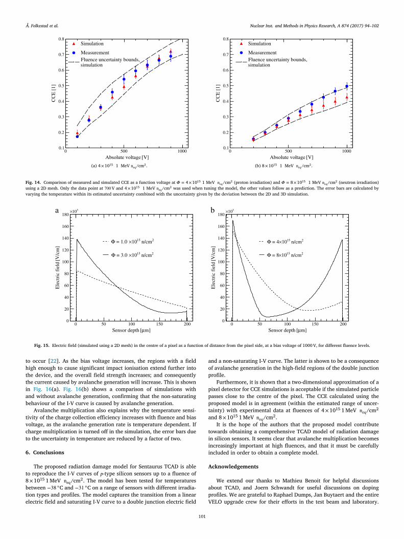
The measured charge collection efficiency for the reference sensor(𝛷 = 4×10¹⁵ 1 MeV neq/cm2) used for tuning the model is shownin Fig. 14(a) together with the simulated CCE (at 𝑇 = −32.1 ◦C). Asdiscussed in Section 2.4, only one CCE measurement (the point at 700 Vbias) was used for tuning the model; the voltage dependence is predictedby the model and is found to be in agreement with the data.
Fig. 14(b) shows simulated and measured CCE as a function ofbias voltage at a fluence of 8×10¹⁵ 1 MeV neq/cm2. The measuredCCE is close to the upper end of the fluence error band of the sim-ulation (i.e. the simulated CCE for a fluence at the lower bound ofthe estimated uncertainty). It should be noted that in Fig. 14(a), thesimulated CCE is compared to a proton-irradiated sensor, whereas at8×1015 1 MeV neq/cm2 it is compared to a neutron-irradiated sensor.
The temperature of the sensors in test beam was known to within±3 ◦C, and the variation in the simulated CCE resulting from varyingthe temperature within this range was factored into the simulation errorbars. At 4×10¹⁵ 1 MeV neq/cm2, the contribution of the temperature un-certainty to the error bars is negligible, while at 8×10¹⁵ 1 MeV neq/cm2
it becomes significant at bias voltages > 500V. In other words, thetemperature dependence of the simulated CCE increases with increasingfluence and bias voltage. An explanation for this observation is given inSection 5.
5. Discussion
Fig. 15 shows the absolute value of the electric field in the pixelcentre as a function of the depth in the sensor for fluences be-tween 1×10¹⁵ 1 MeV neq/cm2 and 8×10¹⁵ 1 MeV neq/cm2. ComparingFigs. 11 and 15, one can see that the double junction develops in thesame fluence range where the leakage current exhibits a transition fromsaturating to non-saturating behaviour. As can be seen from Fig. 15,at the fluence levels characterised by a double junction field, there areregions in the sensor where the electric field exceeds 1 × 10⁵ V cm−1,which is the order of magnitude at which avalanche multiplication starts
100
Å. Folkestad et al. Nuclear Inst. and Methods in Physics Research, A 874 (2017) 94–102
(a) 4×10¹⁵ 1 MeV neq/cm2. (b) 8×10¹⁵ 1 MeV neq/cm2.
Fig. 14. Comparison of measured and simulated CCE as a function voltage at 𝛷 = 4×10¹⁵ 1 MeV neq/cm2 (proton irradiation) and 𝛷 = 8×10¹⁵ 1 MeV neq/cm2 (neutron irradiation)using a 2D mesh. Only the data point at 700V and 4×10¹⁵ 1 MeV neq/cm2 was used when tuning the model, the other values follow as a prediction. The error bars are calculated byvarying the temperature within its estimated uncertainty combined with the uncertainty given by the deviation between the 2D and 3D simulation.
Fig. 15. Electric field (simulated using a 2D mesh) in the centre of a pixel as a function of distance from the pixel side, at a bias voltage of 1000 V, for different fluence levels.
to occur [22]. As the bias voltage increases, the regions with a fieldhigh enough to cause significant impact ionisation extend further intothe device, and the overall field strength increases; and consequentlythe current caused by avalanche generation will increase. This is shownin Fig. 16(a). Fig. 16(b) shows a comparison of simulations withand without avalanche generation, confirming that the non-saturatingbehaviour of the I-V curve is caused by avalanche generation.
Avalanche multiplication also explains why the temperature sensi-tivity of the charge collection efficiency increases with fluence and biasvoltage, as the avalanche generation rate is temperature dependent. Ifcharge multiplication is turned off in the simulation, the error bars dueto the uncertainty in temperature are reduced by a factor of two.
6. Conclusions
The proposed radiation damage model for Sentaurus TCAD is ableto reproduce the I-V curves of 𝑝-type silicon sensors up to a fluence of8×1015 1 MeV neq/cm2. The model has been tested for temperaturesbetween −38 ◦C and −31 ◦C on a range of sensors with different irradia-tion types and profiles. The model captures the transition from a linearelectric field and saturating I-V curve to a double junction electric field
and a non-saturating I-V curve. The latter is shown to be a consequenceof avalanche generation in the high-field regions of the double junctionprofile.
Furthermore, it is shown that a two-dimensional approximation of apixel detector for CCE simulations is acceptable if the simulated particlepasses close to the centre of the pixel. The CCE calculated using theproposed model is in agreement (within the estimated range of uncer-tainty) with experimental data at fluences of 4×10¹⁵ 1 MeV neq/cm2
and 8×10¹⁵ 1 MeV neq/cm2.It is the hope of the authors that the proposed model contribute
towards obtaining a comprehensive TCAD model of radiation damagein silicon sensors. It seems clear that avalanche multiplication becomesincreasingly important at high fluences, and that it must be carefullyincluded in order to obtain a complete model.
Acknowledgements
We extend our thanks to Mathieu Benoit for helpful discussionsabout TCAD, and Joern Schwandt for useful discussions on dopingprofiles. We are grateful to Raphael Dumps, Jan Buytaert and the entireVELO upgrade crew for their efforts in the test beam and laboratory.
101

Å. Folkestad et al. Nuclear Inst. and Methods in Physics Research, A 874 (2017) 94–102
Fig. 16. (a) Impact ionisation generation rate (simulated using a 2D mesh) in the centre of a pixel as a function of distance from the pixel side. (b) simulated I-V curves at 𝑇 = −38.1 ◦Cand 4×10¹⁵ 1 MeV neq/cm2 with and without avalanche generation activated.
This project has received funding from the European Union’s Horizon2020 Research and Innovation programme under Grant Agreement no.654168.
References
[1] LHCb Collaboration. LHCb VELO Upgrade Technical Design Report. CERN-LHCC-2013-021. LHCB-TDR-013, (Nov 2013). URL https://cds.cern.ch/record/1624070.
[2] M. Petasecca, F. Moscatelli, D. Passeri, G.U. Pignatel, Numerical simulation ofradiation damage effects in p-Type and n-Type FZ silicon detectors, IEEE Trans. Nucl.Sci. 53 (5) (2006) 2971–2976. http://dx.doi.org/10.1109/TNS.2006.881910.
[3] F. Moscatelli, D. Passeri, A. Morozzi, R. Mendicino, G.F. Dalla Betta, G.M. Bilei,Combined bulk and surface radiation damage effects at very high fluences in silicondetectors: Measurements and TCAD simulations, IEEE Trans. Nucl. Sci. 63 (5) (2016)2716–2733. http://dx.doi.org/10.1109/TNS.2016.2599560.
[4] D. Pennicard, G. Pellegrini, C. Fleta, R. Bates, V. O’Shea, C. Parkes, N. Tartoni,Simulations of radiation-damaged 3D detectors for the Super-LHC, Nucl. Instrum.Methods Phys. Res. Sect. A 592 (1–2) (2008) 16–25. http://dx.doi.org/10.1016/j.nima.2008.03.100.
[5] R. Eber, Investigations of new Sensor Designs and Development of an effectiveRadiation Damage Model for the Simulation of highly irradiated Silicon ParticleDetectors, Ph.D. thesis, Karlsruhe Institute of Technology, (2013).
[6] T. Peltola, A. Bhardwaj, R. Dalal, R. Eber, T. Eichhorn, K. Lalwani, A. Messineo,M. Printz, K. Ranjan, A method to simulate the observed surface properties ofproton irradiated silicon strip sensors, J. Instrum. 10 (04) (2015) C04025–C04025.http://dx.doi.org/10.1088/1748-0221/10/04/C04025.
[7] D.J. DiMaria, D. Arnold, E. Cartier, Impact ionization and degradation in silicondioxide films on silicon, in: C.R. Helms, B.E. Deal (Eds.), The Physics and Chemistryof SiO2 and the Si-SiO2 Interface 2, Springer US, Boston, MA, 1993, pp. 429–438.
[8] W. Shockley, W.T. Read, Statistics of the recombinations of holes and electrons, Phys.Rev. 87 (1952) 835.
[9] R.N. Hall, Electron-hole recombination in Germanium, Phys. Rev. 87 (1952) 387.[10] R.V. Overstraeten, H.D. Man, Measurement of the ionization rates in diffused silicon
p-n junctions, Solid-State Electron. 13 (5) (1970) 583–608. http://dx.doi.org/10.1016/0038-1101(70)90139-5. URL http://www.sciencedirect.com/science/article/pii/0038110170901395.
[11] J. Slotboom, H. de Graaff, Measurements of bandgap narrowing in Si Bipolartransistors, Solid-State Electron. 19 (1976) 857.
[12] G.A.M. Hurkx, D.B.M. Klaassen, M.P.G. Knuvers, A new recombination model fordevice simulation including tunneling, IEEE Trans. Electron Devices 39 (1992) 331.
[13] Sentaurus Device User Guide, J-2014.09. Synopsys, 2014.[14] V. Eremin, Z. Li, S. Roe, G. Ruggiero, E. Verbitskaya, Double peak electric field
distortion in heavily irradiated silicon strip detectors, Nucl. Instrum. Methods A535 (3) (2004) 622–631. http://dx.doi.org/10.1016/j.nima.2004.06.143. URL http://www.sciencedirect.com/scienc/se/article/pii/S0168900204014627.
[15] V. Eremin, E. Verbitskaya, Z. Li, The origin of double peak electric field distributionin heavily irradiated silicon detectors, Nucl. Instrum. Methods Phys. Res. Sect. A476 (3) (2002) 556–564. http://dx.doi.org/10.1016/S0168-9002(01)01642-4. URLhttp://www.sciencedirect.com/science/article/pii/S0168900201016424.
[16] V. Eremin, Z. Li, I. Iljashenko, Trapping induced Neff and electrical field trans-formation at different temperatures in neutron irradiated high resistivity sili-con detectors, Nucl. Instrum. Methods A 360 (1–2) (1995) 458–462. http://dx.doi.org/10.1016/0168-9002(95)00112-3. URL http://linkinghub.elsevier.com/retrieve/pii/0168900295001123.
[17] G. Lutz, Semiconductor radiation detectors, in: Device Physics Science, Springer,1999, pp. 1–353.
[18] T. Poikela, J. Plosila, T. Westerlund, M. Campbell, M.D. Gaspari, X. Llopart, V.Gromov, R. Kluit, M. van Beuzekom, F. Zappon, V. Zivkovic, C. Brezina, K. Desch, Y.Fu, A. Kruth, Timepix3: a 65K channel hybrid pixel readout chip with simultaneousToA/ToT and sparse readout, JINST 9 (2014) C05013 URL http://stacks.iop.org/1748-0221/9/i=05/a=C05013.
[19] A. Dierlamm, Irradiations in Karlsruhe, (December 2014). URL http://indico.cern.ch/event/86625/contributions/2103519/attachments/1080676/1541436/Irradiations_Ka.pdf.
[20] V. Cindro, Transnational access to TRIGA Mark III reactor at Jof Stefan In-stitute, Ljubljana, (December 2014). URL https://indico.cern.ch/event/342026/contributions/799516/attachments/672081/923628/aida_final_report_ijs.pdf.
[21] M.V.B. Pinto, Caracterizao do Timepix3 e de sensores resistentes radiao para upgradedo VELO, Ph.D. thesis, Universidade Federal do Rio de Janeiro, 2015. URL https://cds.cern.ch/record/2134709.
[22] S.M. Sze, Physics of Semiconductor Devices Physics of Semiconductor Devices,Wiley-Interscience, 1995, pp. 739–751. arXiv:9809069v1.
[23] A. Chilingarov, Temperature dependence of the current generated in Si bulk,JINST 8 (10) (2013) P10003–P10003. http://dx.doi.org/10.1088/1748-0221/8/10/P10003.
[24] S. Wonsak, A. Affolder, G. Casse, P. Dervan, I. Tsurin, M. Wormald, Measurementsof the reverse current of highly irradiated silicon sensors, Nucl. Instrum. MethodsA 796 (2015) 126–130. http://dx.doi.org/10.1016/j.nima.2015.04.027. URL http://www.sciencedirect.com/science/article/pii/S0168900215005008.
102