developing a laser ethernet transceiver to a final
TRANSCRIPT

Developing a laser Ethernet transceiver
to a final prototype assembly

Table of Contents
1. Introduction2. Principle of Operation3. Specification and Requirements4. Transmitter Design5. Receiver Design6. Power Supply Circuit7. Part Selection8. Software9. Administrative Content
2

IntroductionMotivation• Currently more than 15 billion Wi-Fi and cellular devices, estimated to be 100+
billion by 2020 causing a congested network (bandwidth is limited)• Some areas are sensitive to electromagnetic interference• Radio signals can easily be intercepted reducing their security• VLC using lasers is fiber optic ready• The visible spectrum is 100x larger than maximum radio spectrum
i.e. The radio spectrum is 3 Hz - 3 THz whereas VL is 400 - 800 THz (
3
Issues to execution• First thoughts were to make a Li-Fi system, full duplex, and 100 Mbps
speed meaning LEDs transmitting data.
• Originally we attempted to make a 100Base-T system using white LEDs as the data carrier
• Then we attempted to make a 10Base-T version also using white light as the data carrier.
• Each proved to be extremely costly in order to be effective as well as time consuming because of the advanced digital signal processing required.
• There were other factors such as non-linear light to current curves
• Final solution was to make a 10Base-T system using laser diodes
4

LiFi Prototyping and Initial Design
• The transmitter on the breadboard for the 10 Base-T VLC via white LED light.
• Problems include high SNR
• Range of frequency input limited at 10 kHz
• Testing required integration from a surface mounted IC into DIP packaging
• Non-linearity of the light to current curves
5

Prototyping for receiver
The breadboard build of the receiver.
6

Introduction
Real World Implementation• We’ve essentially created a small scale
model with the idea that it could be scaled using different equipment, keeping the same concept, to be used in real world applications
• A company called Koruza currently sells optical transceivers capable of 1-10Gbps speeds.
• In data centers companies are now transitioning to free space optics to connect server racks instead of fiber links
Image courtesy of Koruza
7

Introduction
Goals and Objectives• Create a scale-able wireless Ethernet link using visible light as the carrier
and free space as the medium• Provide a system ready to be integrated into existing infrastructure• Show that our system can wirelessly connect two routers without using
radios• Show that basic VLC systems have comparable speeds to Wi-Fi• Keep the design small and sleek, with low power consumption and
affordable price
8
Introduction
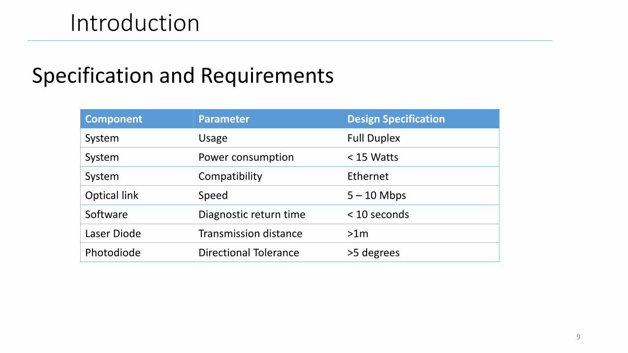
Specification and Requirements
Component Parameter Design Specification
System Usage Full Duplex
System Power consumption < 15 Watts
System Compatibility Ethernet
Optical link Speed 5 – 10 Mbps
Software Diagnostic return time < 10 seconds
Laser Diode Transmission distance >1m
Photodiode Directional Tolerance >5 degrees
9

Principle of Operation
Overall Block Diagram Data Line
Power Line
9V 9V
5V
5V
5V
5V32V
10

Principle of Operation
Input
• 10Base-T signal takes values of -1 or +1• Simplest form of OOK modulation• Sum DC bias of laser diode, with data signal creates modulation• When signal is -1 laser diode is dimmed• When signal is +1 laser diode is brighter
Sample data signal + =DC bias of LD Signal going into LD
11

Principle of Operation
Transmission & Collection
• Signal travels through free space to be collected by the photodiode
• Photodiodes produce current relative to the incident light (intensity)
• With the use of a transimpedance amplifier we convert the current based signal into a voltage based signal
12

Principle of Operation
Output
• After receiving the signal from the transimpedance amp it is sent through one final op amp
• The signal is then sent to the Rx lines of the Ethernet cable in the form of a differential
Ideal signal going into the receiving end of and Ethernet cable
13

Transmitter Design
14

Transmitter Design
Op Amp configuration
• The MAX 4390 is used as a constant current source, by making one of the resistors a potentiometer we can actively adjust the output current.
• This directly powers the laser diode with a DC signal set to about 20 mA
To laser diode15

Transmitter Design
Laser Diode configuration
• The laser diode has a threshold current which creates the stimulated emission process.
• Setting the resistor value we can control the modulation amplitude while above the current threshold.
• We use capacitors to block any kind of DC signal
• We use inductors to prevent the AC signal from reaching any other part of the circuit
16

Receiver Design
17

Receiver Design
Photo Diode configuration
• We reverse bias the photodiode (photoconductive mode), as we increase the bias voltage we decrease the capacitance of the diode and achieve a better response time
• The larger the reverse voltage the greater the dark current
• Passing the output of the photodiode to a transimpedance amplifier makes it ready to be processed
18
To comparator

Receiver Design
Output configuration
• A comparator converts the continuous signal received by the photodiode into discrete values
• The data signal is amplified one last time in order to be properly resolved by an Ethernet device
A sample signal and its output after passing a comparator
19

Power Supply Circuit
• The power supply system consists of a barrel jack, to be connected to a wall outlet, a fuse, a voltage regulator LM78M05CT, and a voltage booster the MIC2605.
• The fuse will break if the voltage regulator or booster is shorted, or overloaded, since these supply the power to the rest of the components they will be protected in this instance.
20

Strategic Components and Part Selections
1. Operational Amplifiers - MAX4390 and MAX4392
2. Transimpedance Amplifier - OPA695
3. Comparator - LT1713
4. Voltage Converter - MIC2605
5. Voltage Regulator - LM78M05CT
6. Photodiode - SFH203
7. Laser Diode - Jameco Valuepro 154145
21

Operational Amplifiers
22
Specifications MAX4390 THS4051 MAX4392 THS4052 OPA695
Operating Temperature
- 40 C to 85 C
- 40 C to 85 C
- 40 C to 85 C
- 40 C to 85 C
- 40 C to 85 C
Cost $1.84 $2.98 $1.20 $5.26 $4.37
Operation Bandwidth
85 MHz 38 MHz 85 MHz 38MHz 450 MHz
Supply Voltage 4.5 – 11 v 9 - 33 V 4.5 - 11 V 9 – 33 V 5 – 12 V
Mounting type
SMT SMT SMT SMT SMT
Channels 1 1 2 2 1
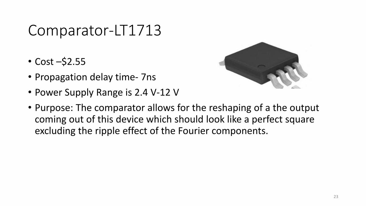
Comparator-LT1713
• Cost –$2.55
• Propagation delay time- 7ns
• Power Supply Range is 2.4 V-12 V
• Purpose: The comparator allows for the reshaping of a the output coming out of this device which should look like a perfect square excluding the ripple effect of the Fourier components.
23
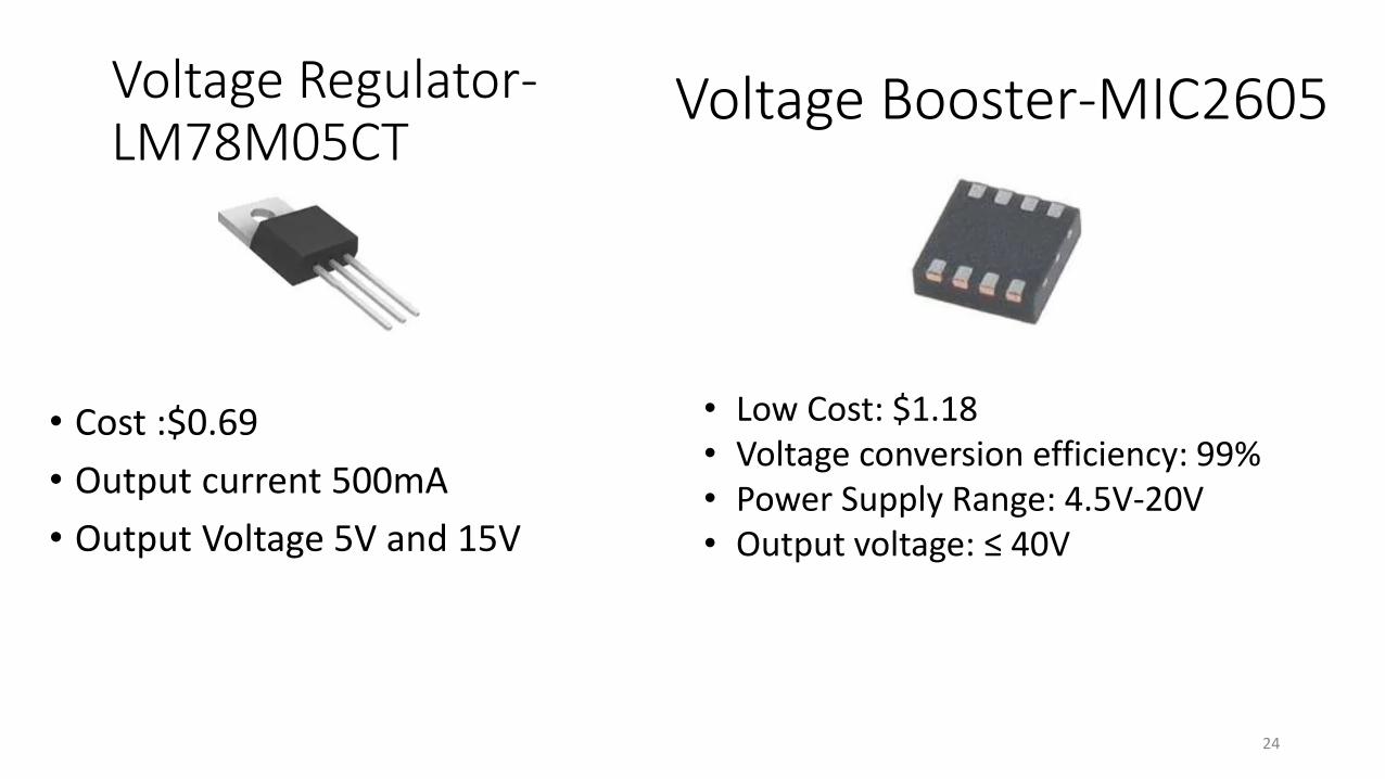
Voltage Regulator-LM78M05CT
• Cost :$0.69
• Output current 500mA
• Output Voltage 5V and 15V
24
• Low Cost: $1.18• Voltage conversion efficiency: 99%• Power Supply Range: 4.5V-20V• Output voltage: ≤ 40V
Voltage Booster-MIC2605

Photodiode- SFH203
• Purpose: To collect the data signal being emitted from the laser diode
25
Specifications BPV10 SFH 203 SXUV5
Operating Temperature - 10 ºC – 40 ºC - 10 ºC – 40 ºC - 10 ºC – 40 ºC
Cost $1.11 $0.29 $363.95
Response, Peak in nm400 – 1100 nm,
950 peak
400 – 1000 nm,
900 peakNear IR, 800 nm
Reverse Voltage 5 – 60 v 5 - 50 V 20 V
Mounting type Through hole Through hole Through hole
Forward Current 70 uA 9.5 uA 10 uA
Frequency Response 250 MHz 270 Mhz 1 GHz
Photodiode Advantage Disadvantage
BPV10Large response range, good
output current
High reverse voltage to
be effective
SFH 203 Cheapest, with good range Low output current
SXUV5Low reverse voltage, very
fast responseExtreme price

Laser-Jameco Valuepro 154145
• Purpose: The laser diode is the modulator for the data, its output acts as the carrier and its modulation is the data
26
Laser Specifications Jameco Valuepro
154145
Lilly Electronics
532MD-30-5V-
TTL
Thorlabs
ML925B45F
Operating Temperature -32.8°C to 149°C +15 ℃ - 35 ℃ -32.8°C to 85°C
Cost $3.49 $25.80 $48.50
Operating Voltage 3 V 5 V 1.5 V
Working Current < 40 mA > 265 mA < 50 mA
Wavelength 650 nm 532 nm 1550 nm
Output Power < 5 mW 30 mW 5 mW
Mounting Type Wires, through
hole 2 pins
Through hole 3
pins
Through hole 3
pins
Photodiode Advantage Disadvantage
Jameco Valuepro
154145
Operating voltage and
current value, low price, 2
pins
Low output power
Lilly Electronics
532MD-30-5V-TTL
High output power High price, high
current required
Thorlabs
ML925B45F
Low current and low
voltage
High price

Device Housing
• The box itself is quite small at only 3" x 3" x 1.5" in the order of length, width, then height.
• The front of the box contains two holes cut out for future lens placement
• The two sides are lined with vents to help keep the electronics cool while in operation.
• There is also a barrel jack opening for the power supply that is not shown in this rendering.
• A lid that is secured by 4 screws to keep the contents safe and locked inside.
27
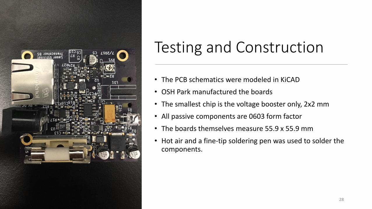
Testing and Construction
• The PCB schematics were modeled in KiCAD
• OSH Park manufactured the boards
• The smallest chip is the voltage booster only, 2x2 mm
• All passive components are 0603 form factor
• The boards themselves measure 55.9 x 55.9 mm
• Hot air and a fine-tip soldering pen was used to solder the components.
28

Software
29

Proposed System & Requirements
• Desktop-based system for file transfer and network information
• Can establish and terminate connection
• Can estimate transfer speed
• Can estimate the file size being sent
• Can check the status of the computers involved
• Can display the network information
30

Software Development Tools
• IDE : Visual Studio
• Language: C#
• Connection: .NET Framework
• OS: Windows
• GUI : Windows Forms
31

Why TCP Protocol?
• TCP vs UDP
• UDP was connectionless, sockets did not need connection.
• TCP needs connections, which it will only function if hardware connects
• FTP is the a layer working on top of the TCP through the application layer, we use a subset of the FTP in our interface
• Also we decided to work with the concept of TCP/IP protocol stack since it is simpler and standardized compared to ISO.
32
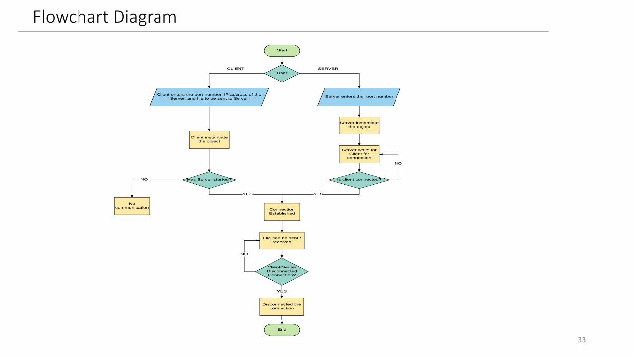
Flowchart Diagram
33

Design of the “TCP/IP Receiver” Side
• The Server GUI will function as the receiver from the Client.
Functionality:
• Start Connection
• Select port number
• Selected location where the file will be saved
34

Design of “TCP/IP Sender” side • The Client GUI is on one side of the
data transmission
• This GUI will provide us with the estimated information of the link communication when data is being transferred
Functionality:
• Select port number
• Select Server's IP address
35

Design of theNetwork Information “Terminal”
• Provides us with the information of the status of whatever network interface we are running on.
• Functionality:
• On the 'Network Interfaces' drop-down menu, select the type of network you want to check during the transmission of data that is executed.
36

Design of the Ping Testing
• The Ping Testing GUI is essential because it would verify if the specific laser Ethernet transceiver will function, essentially if it responds.
• Functionality:
• By writing the user's name on top blank space, we would get the IPv6 address and the time it took to reach the machine.
37

Software Conclusion
• The expectations of the software is that it will work over any network interface even where Visual Light Communication mean is NOT involved.
• This design of the system was made in a simple way so users can visualize the whole purpose of the software.
• GUI is lacking polish, but doesn't affect the goals of the software.
• The system is limited just to a LAN network
• The system is limited to Windows.
38

Administrative Content
Work DistributionRed - Benjamin Stuart and
Garrett BennettBlue - Zhitao Chen
Green - George SalinasPurple electrical and
photonics team
39
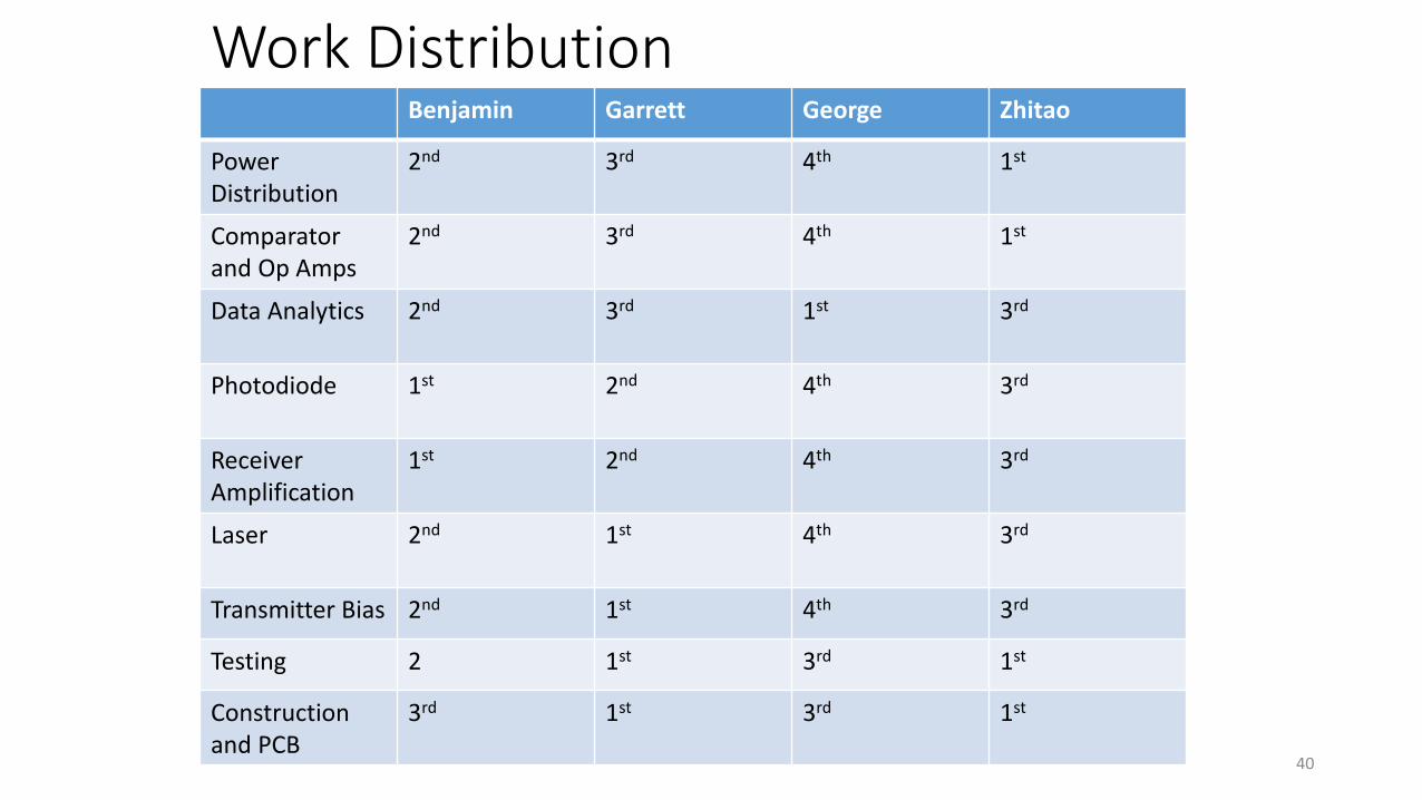
Work DistributionBenjamin Garrett George Zhitao
Power Distribution
2nd 3rd 4th 1st
Comparator and Op Amps
2nd 3rd 4th 1st
Data Analytics 2nd 3rd 1st 3rd
Photodiode 1st 2nd 4th 3rd
ReceiverAmplification
1st 2nd 4th 3rd
Laser 2nd 1st 4th 3rd
Transmitter Bias 2nd 1st 4th 3rd
Testing 2 1st 3rd 1st
Construction and PCB
3rd 1st 3rd 1st
40

Administrative Content
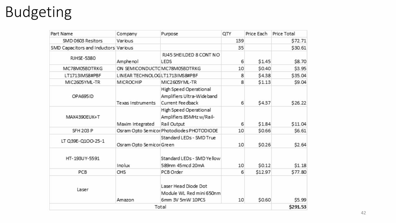
Budget• Overall the cost of the design is $49.69 per board.
• Each component was ordered for the fact that we have six PCB’s and that there would be some initial mistakes in creating such a device for the first time.
• Of course, if there was more of a reason to pursue this product professionally, there are companies which can manufacture every one of the components on to the PCB via machine vision and assembly technology such as smallbatchassembly.com.
• The 500 Ω specialty resistors cost $5.33 each.
41
Budgeting
42

Questions?
43