deterministic trapping, encapsulation and retrieval of single cells · 2017-05-31 · those...
TRANSCRIPT
Lab on a Chip
Supplementary Information
Deterministic trapping, encapsulation and retrieval of single cells M. Sauzade and E. Brouzes
1 METHODS
1.1 CHIP FABRICATION Chips were fabricated following typical protocols.1 Designs were created on Autocad 2000, printed onto
Fuji transparent masks at 25,400 dpi (CAD/Art Services,Inc., OR). We fabricated a photoresist mold on a
3’’ silicon wafer (UniversityWafer, MA) using two steps photolithography. The first layer of negative
photoresist (SU8-2010, MicroChem, MA) was about 12 µm thick, and the second layer (20 µm thick) was
obtained after finely aligning the second mask to overlap with the design of the first one. The master was
treated with a vapor of a fluorinated 1H,1H,2H,2H-Perfluorooctyltrichlorosilane (007146, Oakwood
Chemical, SC) for 90 minutes. A single layer of PDMS (Sylgard 184 Silicone Elastomer Kit, Dow Corning)
obtained by molding was bonded, using an O2 plasma cleaner (Harrick plasma), onto a glass slide
previously spin-coated with PDMS (1,000 rpm for 40 seconds). This ensured comparable surface
properties on the four walls of our circuit.
1.2 SURFACE TREATMENT As our process necessitates a hydrophobic and fluorophilic device, we inject a solution of Novec 17202
(3M) for 20 minutes at 100 µL/h just after bonding; (2) the chip is left to dry at room temperature for 20
minutes; (3) before being placed on a hotplate at 150 degree Celsius for 30 minutes. We found that this
protocol reliably provided high-quality surface treatment, displaying a static contact angle with purified
water of θstatic = 106° +/- 3 (n=16).
The device is reusable by washing the channels with FC40 fluorinated oil and then placing it onto a hot
plate at 100 degree Celsius for a couple hours. Extra care must be given to ensure that no water is present
in the circuit after the washing step. The cleaned device can then be used as such. If the chip is left unused
for more than 10 days, it is recommended to run an additional surface treatment procedure Novec 1720.
1.3 CHIP OPERATION The fluorinated oil, HFE 7500 (3M), is combined with a peg-based krytox surfactant3 at 2% weight to
ensure reproducible droplet generation and stability while guaranteeing good wetting on the treated
walls.
The microfluidic chip is placed on an inverted microscope (Diaphot-TMD, Nikon) and the flow is observed
using a 10X objective (Ph1 10/0.30 DL 160/0.17, Nikon) under bright-field illumination. A 1 mL Gastight
Electronic Supplementary Material (ESI) for Lab on a Chip.This journal is © The Royal Society of Chemistry 2017

syringe (Hamilton) driven by a 290N Nemesys syringe pump (Cetoni GmbH) delivers the flow rate
necessary. Images are recorded using a CCD camera (XCD-V60, Sony).
1.4 NORMALIZED LATERAL POSITION- FIGURE 3 MAIN TEXT The goal is to normalize the position of the center of the cell so that it is null when the cell is in contact
with the wall on the side of the overhang and equal to 1 when sliding against the opposite wall.
Schematic for the normalization of the center of the cell.
If r is the estimated cell radius, yc the position of the center of the cell and wch the width of the channel,
then we define the normalized lateral position of the cell y by:
𝑦 =𝑦𝑐 − 𝑟
𝑤𝑐ℎ − 2𝑟
1.5 CELL CULTURE AND VIABILITY ASSAY Those experiments demonstrate that the trapping-encapsulation strategy developed has a marginal effect
on cell viability with an additional 5-10% of the cells being compromised compared to the control. Finally,
there was no position effect as cell viability did not correlate with specific traps along the circuit.
A498 cells and HeLa cells were maintained in complete medium consisting of Eagle's Minimum Essential Medium (EMEM, Quality Biological 112-018-101 ) and DMEM (Gibco 11965092), respectively, supplemented with 10% fetal bovine serum (Corning 35-011-CV) and 1% Penicillin-Streptomycin (Gibco 15140122) in a standard tissue culture incubator (HERACELL VIOS 160i) at 37 degrees C and 5% CO2.
For device loading, cells are washed with DPBS, after detachment from culture dishes with Accutase (Innovative Cell Technologies) and kept on ice until loading.
Calcein AM (Molecular Probes C1430) and Sytox orange (Molecular Probes S11368) were used to quantify cell viability. Optimal concentrations were found to be 0.2 µM for both dyes. The Live-Dead assays were conducted on a Nikon Eclipse Ti-E, using excitation filters 395/25 and 545/30 and emission filters 460/50 and 620/60 for Calcein AM and Sytox Orange respectively. When both signals were visible, the cell was considered compromised.
1.6 DROPLET VOLUME ESTIMATE- FIGURE 4 MAIN TEXT The volume of a droplet is calculated immediately after generation by multiplying the droplet surface area
by the height of the chamber.
With Sdroplet the droplet surface area, hch the height of the channel and Vdroplet the estimated volume of the
droplet:
𝑉𝑑𝑟𝑜𝑝𝑙𝑒𝑡 = ℎ𝑐ℎ×𝑆𝑑𝑟𝑜𝑝𝑙𝑒𝑡
2 SUPPLEMENTAL FIGURES
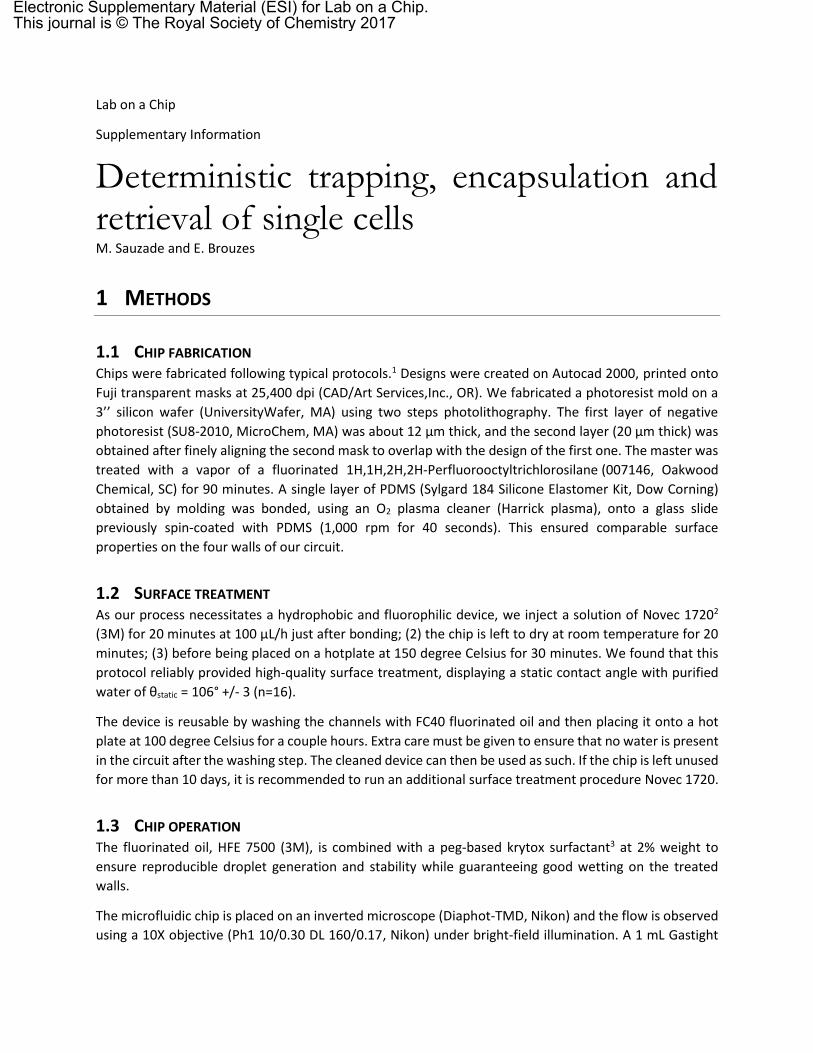
Figure S1. Squeezed out cell during encapsulation. Typically, no droplet is generated when a cell is squeezed out of the trapping channel. See Supplementary movie 3. Scale bar: 50 µm.
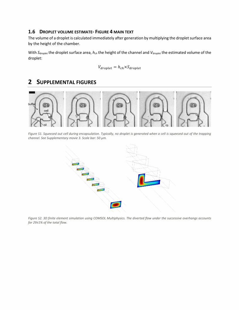
Figure S2. 3D finite element simulation using COMSOL Multiphysics. The diverted flow under the successive overhangs accounts for 29±1% of the total flow.

Figure S3. Impact of the number of overhangs on cell displacement. Comparing the displacement due to 6 overhangs (a) versus a single overhang (b) shows that the latter elicits a smaller displacement of the cells.
Figure S4. 3D finite element simulation using COMSOL Multiphysics. The geometry is based on the actual circuit dimensions. The first two traps are closed to mimic the presence of trapped single-cells. The last two traps are unoccupied and exhibit a flow rate ratio Qtrap/Qbypass = 0.18.

Figure S5. The oil progressing through an empty trap does not generate empty droplets. Scale bar: 50 µm.
Figure S6 Size distribution of HeLa and A498 cells.
Figure S7 Cell viability during trapping and encapsulation as measured by C alcein-AM and Sytox orange staining.
0
10
20
30
40
50
60
70
80
90
100
Control Trapped (n=444) Encapsulated(n=472)
Perc
enta
ge o
f cells
Live Compromised Dead

3 OTHER FILES
3.1 CAD FILE The file Sauzade_Brouzes_SingleCellEncapsulation.dwg contains the design of our device. The layer “0” is
the first layer to be exposed on the wafer, while the layer “1” is the second layer.
3.2 SUPPLEMENTARY VIDEOS Supp. Movie 1: SM1-cell_trapping.avi. Successive trapping of single live A498 cells in the series of
hydrodynamic traps. The movie is displayed at real time.
Supp. Movie 2: SM2-bypass-mode-encapsulation.avi. Successive encapsulation of live A498 cells. The
movie is slowed down 5 times.
Supp. Movie 3: SM3-wetting-mode-encapsulation.avi. Encapsulation of a live A498 cells following the
wetting-driven mode. The movie is accelerated 1.6 fold.
Supp. Movie 4: SM4-cell_squeezed_out.avi. Encapsulation of three single cells followed by the failure of
the encapsulation of the cell in trap #27. The trap where the cell is squeezed out is highlighted by a dark
box throughout the movie.
Supp. Movie 5: SM5-droplet_retrieval.avi. Droplets containing cells retrieval after inverting the oil flow.
The movie is displayed at real time. Scale bar: 50 µm.
4 REFERENCES
1. E. Brouzes, Single-Cell Analysis: Methods and Protocols, 2012, 105-139. 2. A. Mongersun, I. Smeenk, G. Pratx, P. Asuri and P. Abbyad, Anal Chem, 2016, 88, 3257-3263. 3. C. Holtze, A. Rowat, J. Agresti, J. Hutchison, F. Angile, C. Schmitz, S. Köster, H. Duan, K. Humphry
and R. Scanga, Lab Chip, 2008, 8, 1632-1639.