designing with 4g modulated signals for optimized multi …€¦ · optimized multi-standard...
TRANSCRIPT

Designing with 4G Modulated Signals for
Optimized Multi-standard Transceiver ICs
Juergen Hartung
RFIC Product Planning &
Foundry Program Manager
Agilent EEsof
Andy Howard
RFIC Application Development Engineer
Agilent EEsof
© Agilent Technologies 2013
“Designing with 4G Modulated Signals for
Optimized Multi-standard Transceiver ICs”

Agenda
• Introduction
• RF Design Challenges for 4G Systems
• Enabling RF-System Simulation within the RFIC environment
• Going beyond RF System Verification
• Summary
2
Copyright © Agilent Technologies 2013
“Designing with 4G Modulated Signals for
Optimized Multi-standard Transceiver ICs”

Time-to-Market – Today’s Tablets as an example
Data
Wi-Fi® 802.11a/b/g/n
Now: 802.11ac
Personal Connectivity
Bluetooth v4.0
Now: 802.11ad
Location
A-GPS possible: Galileo, Beidou, GLONASS
Communications
4G LTE
Now: LTE-Advanced
HSPA, HSPA+
DC-HSDPA Also: GSM/EDGE, WCDMA,
Multi-Standard Radio (MSR)
o Multiple different complex systems placed in close proximity
o Tight design specs through increased bandwidth
Copyright © Agilent Technologies 2013
“Designing with 4G Modulated Signals for
Optimized Multi-standard Transceiver ICs” 3

Some RF Design Challenges for 4G
• Increased bandwidth to 100 MHz (LTE-A) and 160 MHz (802.11ac)
• Drives Peak-to-Average Power Ratio (PAPR) to extreme levels and requires
Efficiency trade-offs
• Exposes frequency-dependence as well as Memory Effects and Nonlinearities
• No transmit filter definition in LTE, as for 3G technologies
• In-channel performance (i.e. EVM) and out-of-channel performance (i.e. ACLR,
SEM (Spectrum Emission Mask)) requirements need to be met by the design
• Dramatically increased Verification task
• Fragmented spectral bands (e.g. – 43 defined bands for LTE)
• Co-existence with older/multiple standards (MSR testing)
• Advanced compensation techniques require RF/BB interaction
• Digital Pre-Distortion (DPD) or Envelope Tracking
4
Copyright © Agilent Technologies 2013
“Designing with 4G Modulated Signals for
Optimized Multi-standard Transceiver ICs”

Example: Enhancements from 802.11n to 802.11ac
5
Copyright © Agilent Technologies 2013
“Designing with 4G Modulated Signals for
Optimized Multi-standard Transceiver ICs”
Feature Mandatory Optional
Channel bandwidth 20 MHz, 40 MHz, 80 MHz 160 MHz, 80+80 MHz
FFT size 64, 128, 256 512
Data subcarriers / pilots 52 / 4, 108 / 6, 234 / 8 468 / 16
Modulation types BPSK, QPSK, 16QAM, 64QAM 256QAM
MCS supported 0 to 7 8 and 9
Spatial streams 1 2 to 8
…
Modulation Coding Rate 802.11n
EVM (dB)
802.11ac
EVM (dB)
… … … …
64QAM 3/4 -25 -25
64QAM 5/6 -28 -27
256QAM 3/4 N/A -30
256QAM 5/6 N/A -32

RF Design Challenges for 256 QAM Modulation
• 256QAM requires better error vector magnitude (EVM) performance
• Transmitter relative constellation error (EVM) spec for 256QAM is -32 dB vs. -28 dB for 64QAM
• Achieving better EVM requires better linearity and phase noise
• Errors may be due to imperfections in
• IQ modulator,
• phase noise in LO
• amplifier nonlinearity
6
Copyright © Agilent Technologies 2013
“Designing with 4G Modulated Signals for
Optimized Multi-standard Transceiver ICs”
But what means “better” exactly? How do you translate real RF
limitations back up to system-level performances?
Phase noise
I/Q-Imbalance
Quadrature offset

Need for “true” RF System simulations Example: Expand test coverage
• Using modulated signals can point to problems that cannot be uncovered
by traditional RF simulations
7
Copyright © Agilent Technologies 2013
“Designing with 4G Modulated Signals for
Optimized Multi-standard Transceiver ICs”
LNA in the linear region
LNA close to compression
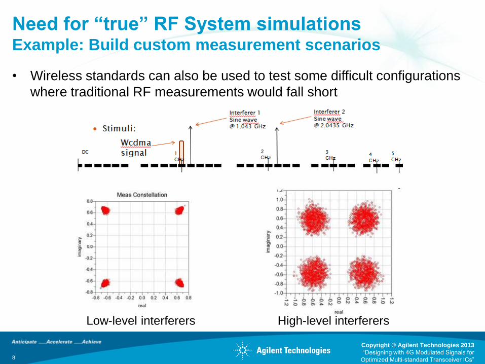
Need for “true” RF System simulations Example: Build custom measurement scenarios
8
Copyright © Agilent Technologies 2013
“Designing with 4G Modulated Signals for
Optimized Multi-standard Transceiver ICs”
Low-level interferers High-level interferers
• Wireless standards can also be used to test some difficult configurations
where traditional RF measurements would fall short

802.11ac Transmitter and Receiver Tests
9
Copyright © Agilent Technologies 2013
“Designing with 4G Modulated Signals for
Optimized Multi-standard Transceiver ICs”
Transmitter Tests
(Section 22.3.19 in 802.11ac std)
• Transmit spectrum mask
• Spectral flatness
• Transmit center frequency tolerance
• Packet alignment
• Symbol clock frequency tolerance
• Modulation accuracy
• Transmit center frequency leakage
• Transmitter constellation error (EVM)
Receiver Tests
(Section 22.3.20 in 802.11ac std)
• Minimum input level sensitivity
• Adjacent channel rejection
• Nonadjacent channel rejection
• Receiver maximum input level
• Clear Channel Assessment (CCA)
sensitivity
No mention of IP3, NF, …!

Need for “true” RF System simulations
In summary:
• Some system specifications are very hard to budget, because it involves mechanisms not modeled in the system simulations
• Example: TX EVM involves third order nonlinearities, am/am and am/pm conversions, spectral regrowth, memory effects … while system studies are mainly based on simple models.
• This usually results in non optimal design (meaning that margin is taken to be “sure” to get the final spec) and potential overdesign (cost in die size, current consumption …)
• Traditional approaches are no longer sufficient
• Example: IM3 is often used as approximation of ACLR
Only solution is to optimize the design monitoring the final spec
• This is particularly true for EVM/ACPR in TX and desensitization in RX
10
Copyright © Agilent Technologies 2013
“Designing with 4G Modulated Signals for
Optimized Multi-standard Transceiver ICs”

Cluttered Design Flows Prevent Efficient
Design & Test
11
Copyright © Agilent Technologies 2013
“Designing with 4G Modulated Signals for
Optimized Multi-standard Transceiver ICs”
Ideas Validated
Design
Measurement
World EDA
World
Mfg
RFIC Implementation
virtual physical
Connecting
Design to
Validation
System Design
RF Test
Pictures are courtesy of Chipworks

Enablement of “true” RF System simulations
OK, I agree with the value of using modulated signals during my
RFIC design, but:
• Can I really run EVM or ACPR measurements in reasonable
simulation times?
• Where do I get modulated signals from and how can I
perform such measurements in my IC environment?
• Does every designer has to understand a wireless standard?
Looking at all these “system” parameters is really
overwhelming!
• Can I perform the same measurement as later in the lab?
12
Copyright © Agilent Technologies 2013
“Designing with 4G Modulated Signals for
Optimized Multi-standard Transceiver ICs”

How to address the simulation speed bottleneck?
• You can’t perform RF System measurements
(ACPR, EVM, …) with HB analysis and
Transient would be too slow
• Envelope analysis can simulate complex
signals much faster than a Transient engine
(> 100x speed-up)
13
Copyright © Agilent Technologies 2013
“Designing with 4G Modulated Signals for
Optimized Multi-standard Transceiver ICs”
• But also “Standard” Envelope engines can’t be used effectively as part of
the design cycle
• GoldenGate offers a “Fast Envelope” option as part of its Envelope
Transient (ET) analysis that provides another dramatic speed
improvement (up to several 1000x)
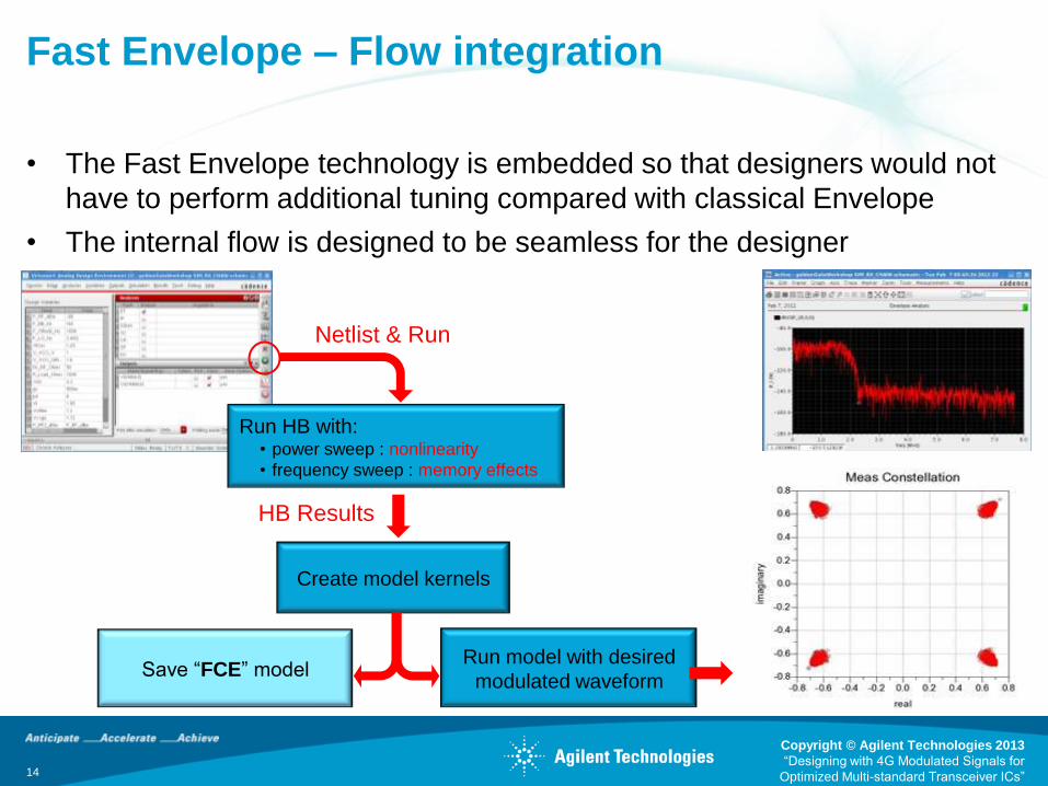
Fast Envelope – Flow integration
14
Copyright © Agilent Technologies 2013
“Designing with 4G Modulated Signals for
Optimized Multi-standard Transceiver ICs”
• The Fast Envelope technology is embedded so that designers would not
have to perform additional tuning compared with classical Envelope
• The internal flow is designed to be seamless for the designer
Run HB with: • power sweep : nonlinearity
• frequency sweep : memory effects
Create model kernels
Netlist & Run
HB Results
Run model with desired
modulated waveform Save “FCE” model
Envelope & Fast Envelope Engines
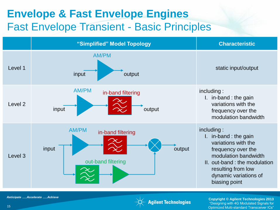
Fast Envelope Transient - Basic Principles
15
Copyright © Agilent Technologies 2013
“Designing with 4G Modulated Signals for
Optimized Multi-standard Transceiver ICs”
“Simplified” Model Topology Characteristic
Level 1 static input/output
Level 2
including :
I. in-band : the gain
variations with the
frequency over the
modulation bandwidth
Level 3
including :
I. in-band : the gain
variations with the
frequency over the
modulation bandwidth
II. out-band : the modulation
resulting from low
dynamic variations of
biasing point
AM/PM
output input
AM/PM
output input
in-band filtering
AM/PM
output input
in-band filtering
out-band filtering

Provide RF System Test benches in an IC
Environment
• GoldenGate offers various approaches to enable standard-compliant system tests
within the Virtuoso platform
• These scalable links support various levels of interaction ranging from simple
input/output file exchange to full co-simulation with data flow engines
• 4G sources and sinks are either available through SystemVue and Agilent test
equipment (Signal Studio / VSA software)
16
Copyright © Agilent Technologies 2013
“Designing with 4G Modulated Signals for
Optimized Multi-standard Transceiver ICs”
Direct Conversion
Receiver
RF Input
Baseband
I&Q Output

Consistent RF System Verification System Design – RFIC Design – Lab Test
17
Copyright © Agilent Technologies 2013
“Designing with 4G Modulated Signals for
Optimized Multi-standard Transceiver ICs”
Direct Conversion
Receiver
RF Input
Baseband
I&Q Output
RFIC in Virtuoso
Signal Generator Signal Analyzer
Signal Studio VSA
Lab Test
WLAN 11ac Receiver Sensitivity Testbench in SystemVue
RF RX
Model
VTB
source
VTB
sink
Read Write
FCE
Cre
ate
cu
sto
m
tes
t s
ign
als
Pictures are courtesy of Chipworks

Enabling RF System simulations for RFIC Designer New Verification Test Benches (VTB)
• VTB are parameterized, pre-configured Test Benches from SystemVue
• Allows RFIC designer using GG to easily validate his circuit performance
against modulated metrics like EVM, BER, or ACPR
• User can also create custom VTBs
18
Copyright © Agilent Technologies 2013
“Designing with 4G Modulated Signals for
Optimized Multi-standard Transceiver ICs”

Enabling RF System simulations for RFIC Designer New Verification Test Benches (VTB)
19
Copyright © Agilent Technologies 2013
“Designing with 4G Modulated Signals for
Optimized Multi-standard Transceiver ICs”
4G pre-configured VTB test benches:
Also other examples are available: ACPR & EVM measurement, QAM16_SER_vs_EbNo

Demo 1: New Verification Test Benches (VTBs)
20
Copyright © Agilent Technologies 2013
“Designing with 4G Modulated Signals for
Optimized Multi-standard Transceiver ICs”
2. Set
“ET Stimulus”
to VTB
1. Setup your ET analysis
3. Select a pre-defined
VTB testbench
4. Run Envelope simulation
5. Results display

Going beyond RF System Verification Leverage Modulated Signals during the Design Phase
• Refine the RFIC specification and optimize your design
against RF-system critical metrics early on
• Demo: Leverage FYC-ET to optimize the ACPR of a Power Amplifier
• Provide an accurate RF model representation back to the
System lead for his comprehensive verification runs
• Demo: FCE model used in an LTE Uplink test in SystemVue
• Using modulated signals to design and optimization
compensation against true system metrics
• Demo: Envelope Tracking
21
Copyright © Agilent Technologies 2013
“Designing with 4G Modulated Signals for
Optimized Multi-standard Transceiver ICs”

Optimize your design against RF-system metrics Fast Yield Contributor (FYC)
22
Copyright © Agilent Technologies 2013
“Designing with 4G Modulated Signals for
Optimized Multi-standard Transceiver ICs”
• GoldenGate provides a Fast
Monte Carlo analysis mode
• FYC permits fast mismatch &
process variation analysis
– Up to 60X speed improvement in
harmonic-balance simulations
– Little to no loss in accuracy
• Contribution Tables can optionally
be produced
– Provide detailed breakout of the
impact of each device in the design

Demo 2: Using FYC in Envelope to optimize ACPR
23
Copyright © Agilent Technologies 2013
“Designing with 4G Modulated Signals for
Optimized Multi-standard Transceiver ICs”
R1 and R5 = 380 Ohms
R1 and R5 = 300 Ohms
R1 & R5 show most contribution
Histograms of Output Power and ACPR for different R1 and R5 values
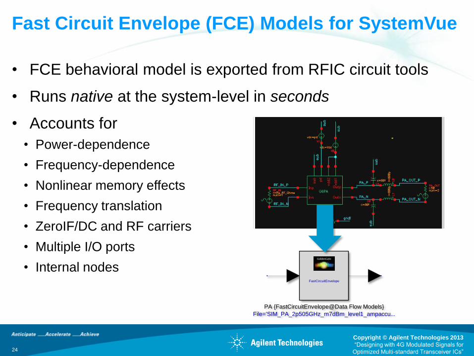
Fast Circuit Envelope (FCE) Models for SystemVue
24
Copyright © Agilent Technologies 2013
“Designing with 4G Modulated Signals for
Optimized Multi-standard Transceiver ICs”
• FCE behavioral model is exported from RFIC circuit tools
• Runs native at the system-level in seconds
• Accounts for
• Power-dependence
• Frequency-dependence
• Nonlinear memory effects
• Frequency translation
• ZeroIF/DC and RF carriers
• Multiple I/O ports
• Internal nodes FastCircuitEnvelope
File='SIM_PA_2p505GHz_m7dBm_level1_ampaccu...
PA {FastCircuitEnvelope@Data Flow Models}

Demo 3: FCE model used in an LTE Uplink test
25
Copyright © Agilent Technologies 2013
“Designing with 4G Modulated Signals for
Optimized Multi-standard Transceiver ICs”
123
StartStopOption=Samples
BB_Sig
1 1 0 1 0
DataPattern=PN9
B3 {DataPattern@Data Flow Models}
1 1 0 1 0
DataPattern=PN9
B2 {DataPattern@Data Flow Models}
1 1 0 1 0
DataPattern=PN9
B1 {DataPattern@Data Flow Models}
1 1 0 1 0
DataPattern=PN9
B4 {DataPattern@Data Flow Models}
LTE Uplink Transmitter Measurements
HARQ_Bits
DataIn
RI_In
HARQACK_In
CQI_In
Frame
FRM_FD
Data_FD
PUSCH_ModSymbols
SC_Status
PUSCH_ChannelBits
LTE
UL
Src
PUSCH_n_DMRS2=0 [[0]]
PUSCH_n_DMRS1=0 [[0]]
PUSCH_Delta_ss=0
SeqHop_Enable=NOGroupHop_Enable=NO
RB_Alloc=0;25 [[0, 25]]
RB_AllocTy pe=StartRB + NumRBs
PUSCH_TransMode=Data and Control Multiplexing
PUSCH_HoppingEnable=NO
MappingTy pe=0;0;0;0;0;0;0;0;0;0 [[0, 0, 0, 0, 0, 0, 0, 0, 0, 0]]PUCCH_PUSCH=PUSCH
FrameIncreased=NO
FrameNum=0
n_RNTI=0
CellID_Group=0
CellID_Sector=0Cy clicPref ix=Normal
Ov ersamplingOption=Ratio 2 [Ov ersamplingOption]
Bandwidth=BW 5 MHz [Bandwidth]
FrameMode=FDD
LTE_UL_Src_1 {LTE_UL_Src@LTE 8.9 Models}
Spectrum Analyzer
ResBW=30000Hz
Start=0ms [Start_Time]Mode=ResBW
SpectrumAnalyzer
CCDF
Stop=0.01s [Stop_Time]
Start=0s [Start_Time]
CCDF
Re
Im
CxToRect
Adjust input signal magnitude
SampleRate=15.36e+6Hz [SamplingRate]
Power=0.01W
Frequency =2.505GHzO1
Manage-Model1. GoldenGate Cosim2. FCE level 1, amplitude accuracy 52. FCE level 3, amplitude accuracy 5, frequency accuracy 12. FCE level 3, amplitude accuracy 5, frequency accuracy 2
FastCircuitEnvelope
File='SIM_PA_2p505GHz_m7dBm_lev el1_ampaccu...
PA {FastCircuitEnv elope@Data Flow Models}
ModOUT
QUAD
OUT
FreqPhaseQ
I
Amp
InputTy pe=I/Q
Modulator
VSA_89600_Sink
VSATitle='Simulation output
V1 {VSA_89600_Sink@Data Flow Models}
NomGain = -15
-50 -15
Gain=0.178 [10 (̂NomGain/20)]
G1 {Gain@Data Flow Models}
Coded LTE UL
5 MHz source
SystemVue W1910/W1918 library
RFIC CMOS PA
“FastCircuitEnvelope” model
exported from GoldenGate
89600 VSA
LTE demod
TUNE MODE
SCRIPTABLE ENVIRONMENT
SCRIPTABLE PARAMETERS

Reliable system-level performance in seconds
26
Copyright © Agilent Technologies 2013
“Designing with 4G Modulated Signals for
Optimized Multi-standard Transceiver ICs”
Pout = +19.3dBm, ACLR=23dBc
CPU time = 3 sec (150k points)
Pout = +10.6dBm, ACLR=37dBc
CPU time = 3 sec (150k points)
Nominal LTE result (0.4% EVM) LTE result – Compressing PA (20% EVM)

Demo 4: Using modulated signals for Envelope
Tracking
27
Copyright © Agilent Technologies 2013
“Designing with 4G Modulated Signals for
Optimized Multi-standard Transceiver ICs”
Simulate power
amplifier with
modulated input signal
and corresponding
envelope tracking bias
voltage
Summary
• Bridging design and system-level verification by introducing
new formalisms & technologies
• Fast Envelope enables reasonable simulation performance
for “true” RF System measurements at IC level
• Pre-defined test benches allow RFIC designer to easily
validate RF system performance specs
• Provides a complete solution across System Design, RFIC
Design and Lab Test
Go and try it out yourself!!
28
Copyright © Agilent Technologies 2013
“Designing with 4G Modulated Signals for
Optimized Multi-standard Transceiver ICs”
Additional Resources
29
Copyright © Agilent Technologies 2013
“Designing with 4G Modulated Signals for
Optimized Multi-standard Transceiver ICs”
• GoldenGate: http://www.agilent.com/find/eesof-goldengate
• SystemVue: http://www.agilent.com/find/eesof-systemvue
• Previous webcasts on this topic:
• LTE-Advanced: Overcoming Design Challenges for 4G PHY Architectures
• Accelerate 802.11ac/ad System-Level Design & Verification for Next-
Generation WLAN
• Memory Effects in RF Circuits: Manifestations and Simulation
• A Model Based Approach for System Level RFIC Verification
• A Practical Approach to Verifying RFICs with Fast Mismatch Analysis
• RF Power Amplifier Design Series: Part 5: Envelope Tracking Simulation
and Analysis
• YouTube Video: “Fast Circuit Envelope Models for RFIC verification” http://www.youtube.com/watch?v=7k8TS2Due70

You are invited to our next webcast
Register for our live and recorded webcasts here:
www.agilent.com/find/eesof-innovations-in-eda
www.agilent.com/find/eesof-webcasts-recorded
Automating SPICE Library Validation
October 22 – 10AM PT
Shuang Cai
Device Modeling
Application Engineer
Agilent EEsof EDA
Thank you
Please complete the short survey following the end of this webcast.