designing biomedical imaging hardware using network …save.seecs.nust.edu.pk/downloads/uzma...
TRANSCRIPT

DESIGNING BIOMEDICAL IMAGING HARDWARE
USING NETWORK on CHIP (NoC)
By
UzmaMushtaq
2009-NUST-MSEE(S)-27
Supervisor
Dr. Osman Hasan
A thesis submitted in the partial fulfillment of the requirements for the degree of
Masters of Electrical Engineering (MSEE)
School of Electrical Engineering and Computer Science (SEECS)
National University of Sciences and Technology (NUST)
January 2012

IN THE NAME OF ALLAH
THE MOST GRACIOUS
THE MOST MERCIFUL

IV
Certificate
Certified that the contents of thesis document titled “DESIGNING BIOMEDICAL
IMAGING HARDWARE USING NETWORK on CHIP (NoC) ” submitted by Miss
UzmaMushtaqhas been found satisfactory for the requirement of degree.
Advisor: Osman Hasan
Committee Member1: Dr. Rehan Hafiz
Committee Member2: Dr. ShahzadYounis
Committee Member3: Dr. HammadQureshi
NUSTSchool of Electrical Engineering and Computer Sciences A center of excellence for quality education and research

IV
DEDICATION
Dedicated to my parents, my husband, friends and
teachers who helped us a lot in every field and in every
step of our lives.

V
CERTIFICATE OF ORIGINALITY
I here by declare that the research paper titled “DESIGNING BIOMEDICAL
IMAGING HARDWARE USING NETWORK on CHIP (NoC)” my own hard work
and to the best of my knowledge. It contains no materials which was
previously published or was written by another person, nor material which to
a certain extent has been accepted for the award of any degree or diploma at
NIIT or any other education institute, except where due acknowledgment, is
made in the thesis. Any other contribution made to the research by others,
with whom I have worked at NIIT or elsewhere, is explicitly acknowledged in
the thesis.
I also declare that the intellectual content of this thesis is the product of my
own work, except to the extent that assistance from others in the project’s
design and conception or in style, presentation and linguistic is acknowledged.
I also verified the originality of contents through plagiarism software.
Author Name: UzmaMushtaq
Signature: ______________

VI
Acknowledgement
I would like to thank Almighty Allah, who is the most beneficent and the greatest forgiver,
who guided me in through every difficulty.
At the beginning I was totally unaware what to do but thanks to my project supervisor Dr.
Osman Hasan and co-supervisor Dr.FalahAwwad who lead me to the correct direction and
extended every support to me any time I needed it.
I would like to express my gratitude to Dr. ShahzadYounis and Dr. Rehan Hafiz, who co-
operated with me and helped me in every aspect of my thesis.
The hand of Dr. Habeel Ahmed behind the scene was always a reason for me to do what I
did in SEECS. He made sure that every facility is extended towards the students even in
late hours and through internet as well.
I would also like to thank all the teachers who taught me in my two years of education and
made me capable of doing all this.
It was all possible because of the support of my friends morally and technically. And more
importantly I express my extreme gratitude towards my family. I want to thank my husband
as his patience, support, and, tolerance was the driving force for me. Without him I would
have not been able to do all this work.

VII
TABLE OF CONTENTS ACKNOWLEDGEMENT VI
TABLE OF CONTENT VII
LIST OF ABBREVIATIONS VIII
LIST OF FIGURES IX
LIST OF TABLES XI
ABSTRACT XII
CHAPTER #1 INTRODUCTION 1
1.1 Motivation 2
1.2 Problem Statement 3
1.3 Proposed Solution 3
1.4 Outline Of The Report 4
CHAPTER # 2 LITERATURE REVIEW 5
2.1 NoC 6
2.2 B-Spline 10
CHAPTER # 3 METHODOLOGY 15
3.1 Implementation of PNoc 16
3.2 Implementation of FFD 25
3.3 Implementation of FFD on PNoC 35
CHAPTER # 4 RESULTS AND DISCUSSION 44
CHAPTER # 5 CONCLUSION AND FUTURE WORK 51
5.1 Conclusion 52
5.2 Future Work 53
REFERENCES 54
APPENDIX 1 60
Affine Transformation 60
APPENDIX 2 61
Optimization steps for the cost function transformation 61

VIII
LIST OF ABBREVIATIONS
3-D Three Dimensional
CDG Communication Dependency Graph
CP Control Point
FFD Free Form Deformations
FIFO First In First Out
FSM Finite State Machine
GP Grey Point
LUT Look Up Table
MI Mutual Information
MLD Mission Level Designer
MRI Magnetic Resonance Imaging
NMI Normalized Mutual Information
NoC Network on Chip
PNoC Programmable Network on Chip
PETCT Positron Emission Tomography and Computerized Tomography
S&F Store and Forward
VC Virtual Channel

IX
LIST OF FIGURES
FIG 2.1: Example of NoC 8
FIG 2.2: Switching Techniques 10
FIG 3.1: PNoC network topology 17
FIG 3.2: Snapshot of router 18
FIG 3.3: Buffer 19
FIG 3.4: Verilog modules for PNoC 20
FIG 3.5: FIFO control 21
FIG 3.6: Memory 22
FIG 3.7: Mux 23
FIG 3.8: Simulation diagram of NoC 24
FIG 3.9: Pipelined system for FFD computation 25
FIG 3.10: Pixels of image under the influence of control point lattice 26
FIG 3.11: FFD Verilog modules 27
FIG 3.12: B-Spline LUT 28
FIG 3.13: Calculating B for 16 input pixels 29
FIG 3.14: Memory contents of image file 30
FIG 3.15: loop code 31
FIG 3.16: FFD module 32

X
FIG 3.17: FFD module another view 33
FIG 3.18: Simulation diagram for FFD 34
FIG 3.19: PNoC architecture for FFD 35
FIG 3.20: FFD on PNoC schematic 37
FIG 3.21: Main module of FFD on PNoC (1) 38
FIG 3.22: Main module of FFD on PNoC (2) 39
FIG 3.23: Main module of FFD on PNoC (3) 40
FIG 3.24: Value of output pixels for first 310ns 41
FIG 3.25: Value of output pixels from 520-630ns 42
FIG 3.26: Value of output pixels from 670-790ns 43
FIG 4.1: Xilinx simulation report for NoC 45
FIG 4.2: Simulation report for FFD 47
FIG 4.3: Xilinx simulation report for FFD on PNoC 49
XI
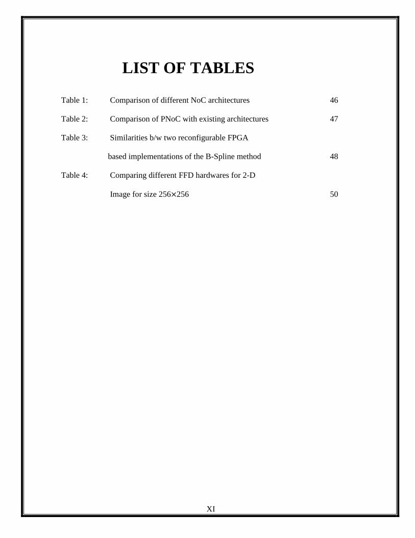
LIST OF TABLES
Table 1: Comparison of different NoC architectures 46
Table 2: Comparison of PNoC with existing architectures 47
Table 3: Similarities b/w two reconfigurable FPGA
based implementations of the B-Spline method 48
Table 4: Comparing different FFD hardwares for 2-D
Image for size 256 256 50

XII
ABSTRACT
The document describes the technique for implementing FFDs on NoC. The FFD
technique uses B-spline algorithm for the modeling of 3-D deformable objects. Until
now reconfigurable hardware like FPGA has not been applied widely to the area of
image registration. Fixed-point implementation is required for effective
implementation and high speed. The NoC described is lightweight circuit-switched
architecture called PNoC. PNoC is a very flexible architecture that suits the FPGA-
based systems. Our design description is captured in Verilog language and
implemented on Xilinx XC2V6000 device at 37 MHz is parametrizable at the compile
time and supports a range of the image resolutions and computational precisions.

1
Chapter # 1
INTRODUCTION Motivation
Problem Statement
Proposed Solution
Outline of the Report
2
Chapter # 1 Introduction
This project is aimed at implementing medical imaging application on NoC. There are
three phases in the system-NoC implementation, FFD implementation and Implementation
of FFD on NoC.
1.1 Motivation
Free Form Deformation (FFD) [1, 2] based algorithms are primarily used for modeling
geometric shapes in a computerized environment. Recently, FFD algorithms have found
many interesting applications in the domain of medical imaging.
Traditionally, in the medical domain, multiple radiological images of a patient are acquired,
printed and then analyzed by viewing them on a light box. However, the computer based
image registration techniques [2,4] are increasingly being used these days in the area of
medical imaging as they offer significant benefits for aligning different images together
and for visualizing their combined images. For example, it is quite difficult to localize
tumors using CT and MR scans based images because the contrast between the tumor and
its surrounding tissues is of very low intensity [1,2]. However, image registration has been
shown to enhance the tumor detection significantly [3,4].

3
1.2 Problem Statement
Medical image registration methods are primarily based on iterative algorithms that tend to
minimize some cost or energy factor, which is usually defined in terms of thedifference of
geometry or intensity between images. Thus, the efficiency of image registration is directly
dependent on the performance of the underlying algorithms. A significant amount of
research has been conducted to explore efficient algorithms for medical image registration.
For example, a non-rigid registration algorithm based on the FFD and modeled by B-
splines is explained in [5]. Similarly, another algorithm for the non-rigid registration of 3-D
breast MRI is investigated in [6]. This work is based on normalized mutual information.
One of the common problems associated with the image registration algorithms is their
enormous computation complexity due to the high resolution and complex nature of the
medical images that are to be analyzed. For example, processing a 3D image of
256x256x64 voxels takes 15-30 minutes to be processed using the FFD algorithm, which
acts as a local motion model in this context, on a Sun Ultra 10 workstation [7].
1.3 Proposed Solution
In order to overcome the above mentioned computation time limitation, dedicated hardware
platforms have been proposed to be used for executing non-rigid image registration
algorithms [1,3,4]. Due to the vast applicability of FFD based algorithms; one of the prime
objectives of this research has been to optimize the performance of FFD algorithms by

4
modeling them on hardware platforms [8,9]. One of the most recent works, oriented
towards this direction of research is the reconfigurable hardware based FPGAs
implementation to compute the B-spline based FFDs for medical imaging [7]. The current
thesis contributes towards enhancing the performance of the B-spline based FFD algorithm
further as we propose to use a Network-on-Chip (NoC) [10,11] based hardware
implementation for this purpose.
1.4 Outline of the Report
The rest of the report is organized as follows: Chapter 2 provides literature review of the
NoC architectures and the B-Spline FFD algorithm. We present the methodology in chapter
3. Chapter 4 describes the results. In chapter 5, we present the conclusions and future work.

5
Chapter # 2
Literature Review NoC
B-Spline based FFD

6
Chapter # 2 Literature Review
2.1 NoC
The NoC technology tends to provide high performance and low power consumption for
system-on-chip architectures. NoCs have been implemented in different configurations and
provide various capabilities. This section provides a summary of some of the existing NoC
architectures.
Xpipes [10] architecture is based on a heterogeneous model unlike NoCs, which are
primarily based on a homogeneous model. Due to its heterogeneous nature, Xpipes requires
an enormous amount of effort during the implementation phase. Agarwal and Shankar
exploited the high performance computing capability of NoCs and proposed a layered
architecture for the NoC based systems [11]. Their architecture constitutes different
domains, including protocol on a NoC environment, algorithms, applications, and RTOS.
Their proposed design was parametrized. This implementation uses Mission Level
Designer (MLD), which is not a commonly used environment and thus is not suitable for
our development where we want to provide a generic NoC implementation. One of the
commercially available NoC is Arteries. [23]. However, using Arteris involves hefty
licensing fee due to its commercial nature. The virtual channel (VC) is an important
ingredient 0f NoC. Bjerregaard proposed a new model for a router for virtual channel and
used the asynchronous techniques for the circuit layout on hardware[24,25]. Mapping
hardware onto this kind of an asynchronous circuit involves significant amount of design

7
efforts. Al-Tawil provides a survey of different switching techniques with main
emphasison wormhole routing technique [22]. The CLICHÉ NoC implementation uses
store-and-forward (S&F) switching [21]. This type of technique uses a huge buffer area
available at every node. Millberg implemented Nostrum NoC using S&F switching [26].
Various switching techniques can be combined to develop Ad-hoc switching techniques
[27,28]. Siebenborn used Communication Dependency Graph (CDG) for inter-process
communications [29]. For using the CDG, we have to perform load balancing, placement,
and fanout routing, which is quite cumbersome. Neeb compared torus, mesh, and cube
networks [30].
In this thesis, our focus is on a NoC based implementation of a FFD algorithm and thus for
this purpose, our requirement is to use a flexible and lightweight NoC architecture. Most of
the above mentioned NoC architectures, are either too complex to be used for this specific
purpose or are not very generic. To fulfill our requirements, we identified a lightweight
circuit-switched NoC for FPGA based systems, described by Hilton and Nelson in [13].
This architecture, called programmable NoC or the PnoC, is designed having three goals in
mind. Firstly, the approach is flexible. Secondly, it is a simple architecture that uses
standardize interfaces for network and simplified protocols. Finally, it offers a lightweight
network, that require a low number of FPGA sources, and is available for smaller as well as
FPGA-based systems on larger scale. However, the architecture has been described using

8
JHDL, which is not a commonly used HDL. In order to facilitate broad usage of PNoC
proposed in [13], we ported its design to Verilog in the current thesis and then used this
ported model todevelop the NoC based implementation of the B-Spline FFD algorithm.
As the system complexity increases, the bus based communication systems are not efficient
in terms of scalability, and design and verification times. Moreover, the demand for higher
computational speeds and lower power consumption is essentially required in most of the
consumer electronics and medical equipment. The NoC technology provides a possible
solution to all these problems.
The basic ingredients of a NoC architecture, depicted in Fig. 2.1, include the processing
elements, connection topology, routing technique, switches, and programming model.

9
Fig. 2.1 Example of NoC
There are various connection topologies from the communication perspective. Torus,
octagon, mesh, ring, and irregular connection networks are some of the communication
topologies [16, 17]. Several researches have shown that the 2-D mesh architecture is easy
to implement and provides the most efficient solution for low latency [18].
Different architectures for routing have been proposed but the most widely used ones are
packet switched and circuit switched. The packet switched routing architecture [19]
requires some amount of buffering. Buffers are provided at input, output or both input and
input. In the circuit switched architecture [20], there is a dedicated channel for the data
flow so no buffering or queuing is required.
10
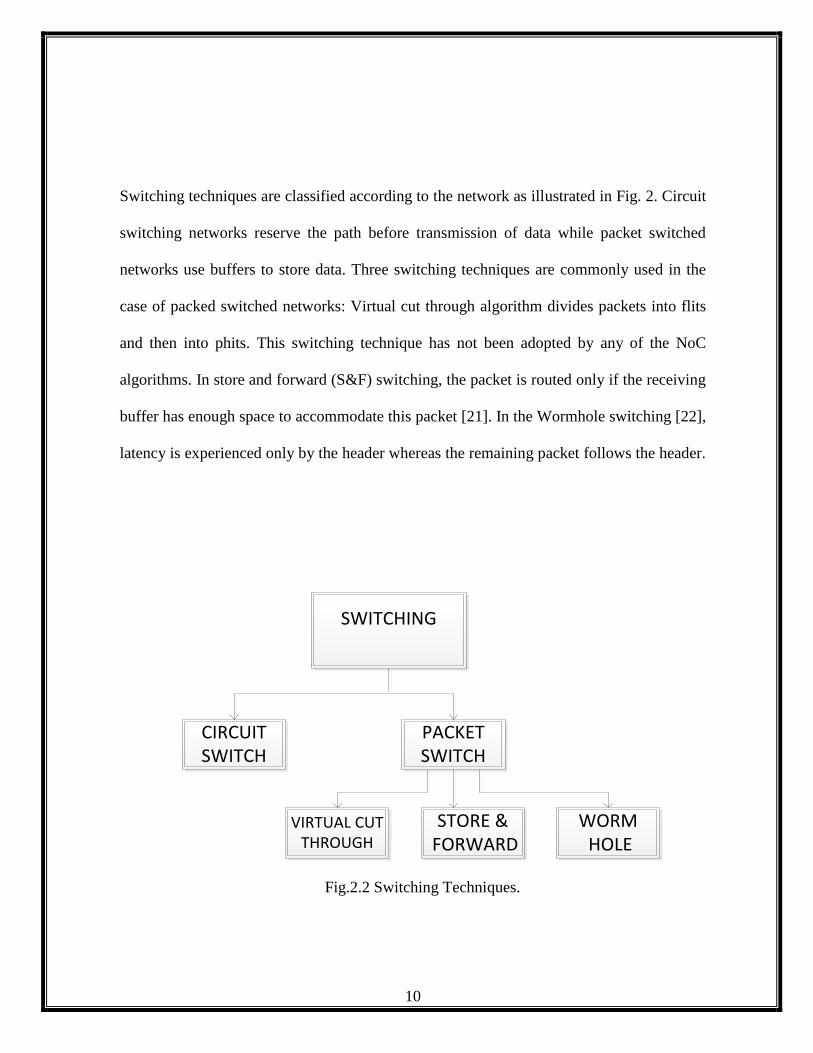
Switching techniques are classified according to the network as illustrated in Fig. 2. Circuit
switching networks reserve the path before transmission of data while packet switched
networks use buffers to store data. Three switching techniques are commonly used in the
case of packed switched networks: Virtual cut through algorithm divides packets into flits
and then into phits. This switching technique has not been adopted by any of the NoC
algorithms. In store and forward (S&F) switching, the packet is routed only if the receiving
buffer has enough space to accommodate this packet [21]. In the Wormhole switching [22],
latency is experienced only by the header whereas the remaining packet follows the header.
SWITCHING
CIRCUIT SWITCH
PACKET SWITCH
VIRTUAL CUT
THROUGH
STORE & FORWARD
WORM HOLE
Fig.2.2 Switching Techniques.
11
2.2 B-Spline based FFD
The computer based image registration techniques [2,4] are increasingly being used these
days in the area of medical imaging as they offer significant benefits for aligning different
images together and for visualizing their combined images. For example, it is quite difficult
to localize tumors using Computer Tomography and Magnetic Resonance scans based
images because the contrast b/w the tumor area and its subsequent tissues is of very low
intensity [1,2]. However, image registration has been shown to enhance the tumor detection
significantly [3,4].
Medical image registration methods are primarily based on iterative algorithms that tend to
minimize some cost or energy factor, which is usually defined in terms of the difference of
geometry or intensity between images. Thus, the efficiency of image registration is directly
dependent on the performance of the underlying algorithms. A significant amount of
research has been conducted to explore efficient algorithms for medical image registration.
For example, a non-rigid registration algorithm based on the FFD and modeled by B-
splines is explained in [5]. Similarly, another algorithm for the non-rigid registration of 3-D
breast MRI is investigated in [6]. This work is based on normalized mutual information.
One of the common problems associated with the image registration algorithms is their
enormous computation complexity due to the high resolution and complex nature of the
medical images that are to be analyzed. For example, processing a 3D image of

12
256x256x64 voxels takes 15-30 minutes to be processed using the FFD algorithm, which
acts as a local motion model in this context, on a Sun Ultra 10 workstation [7].
The B-Spline based FFD algorithm is considered to be one of the most powerful techniques
for modeling 3-D deformable objects in the domain of non-rigid image registration [6],
which is a special kind of image registration used specifically for images with nonlinear
geometric differences. The main motivation behind the optimization of this algorithm in the
current thesis is the increasing utilization of non-rigid registration for the analysis of brain
images and thus an associated enormous performance requirement to be able to analyze
huge and complex brain images.
For non-rigid image registration only rigid or affine transformation (see appendix 1) is not
sufficient for motion correction. A combined transformation (T) using global and local
transformation is used [6].
In FFD, a grid of control points is used to deform an object.For B-Spline FFD image
volume is defined as . denotes the mesh
of control points .The FFD is written as the product of 3 1D cubic B-Splines

13
Where
And
Birepresents ith
basis function as follows:
Where
The image intensities might change between the pre-contrast and the post-contrast image so
direct image intensity comparisons as sum of squared differences (SSD) or correlation
cannot be used. Mutual Information (MI) can be chosen as a similarity measurement to
measure the extent of alignment between the images. NMI (Normalized Mutual
Information) has been recommended to be used for image alignment to remove any
dependence on the quantity of overlap of the images[6].

14
+ + + (5)
We minimize the cost equation connected with local and global parameters of
transformation in order to find the optimal transformation(see appendix 2). The
term , given in Equation (4), corresponds to the image similarity, while the term
, given in Equation (5), corresponds to the image smoothness.
In the above equation the weighing parameter λ shows the tradeoff between transformation
smoothness and the alignment between image volumes, θ represents the global
transformation parameter, and, represents the local transformation parameter

15
Chapter # 3
Methodology Implementation of PNoC
Implementation of FFD
Implementation of FFD on PNoC

16
Chapter # 3 METHODOLOGY
3.1 Implementation of NoC
The NoC technology tends to provide high performance and low power consumption for
system-on-chip architectures. NoCs have been implemented in different configurations and
provide various capabilities.
PNoC is a circuit switched technique that simplifies system design by providing flexible
networking approach and is efficient in design and verification methodologies. The
network consists of subnets, in which each subnet has one router and a bunch of nodes for
network as in Figure 3.1.
The circuit switching between the nodes is performed by the router and every node is
connected to the router by the router-port interface For the connection a dedicated
connection is established using light handshaking mechanism for the data exchange and
connection removal.
The connection is established when mater node A sends the request signal along with the
address of the target node to the router. The second router sends the grant signal to first
router that port B is available and the connection is established.
A dedicated connection path is used for data transfer so no acknowledge signal is required.
Data transaction can occur on successive clock cycles if master rx c ts is low. The read and
write requests can be pipelined.

17
Fig. 3.1 PNoC Network Topology
The router is the main component of the PNoC. The router includes the routing table,
queue, and switch box. The snapshot for the router is shown in figure 3.2.
A CPU is connected to the PNoC like any other module. The interfacing circuit constitutes
FIFO’s and FSM to communicate with the router.

18
Fig 3.2. Snapshot of the router
Another part of the PNoC is the buffer which is a parametrizable feature. Buffer is
necessary in two cases. Firstly, if nodes and routers are running at different clock rates, and

19
secondly, when there is a difference between the transmitting and receiving rate. The
snapshot of our Xilinx implementation of the buffer is shown in Figure 3.3. The buffer
consists of address pointer, memory pointer, buffer full and buffer empty signals.
Fig. 3.3 Buffer
Our Verilog code consists of 1 main or top level Router module and three sub-modules and
its overall structure is illustrated in Figure 3.4.

20
MUXFor Selection of data
lines
ROUTERoute for data to
take
BUFFERFOR queuing and storage of data
MemoryFor storage of
data
FIFOCONTROLFor controlling buffer signals
TOP LEVEL MODULEROUTER
Fig. 3.4 Verilog Modules for PNoC
The Buffer module performs two main functionalities, i.e., FIFO control and the memory.
This FIFO control monitors different signals for the buffers like the buffer empty, buffer
full, memory pointer etc.

21
Fig.3.5 Fifo Control
The memory is used to store the data that comes into the buffer.

22
Fig. 3.6 memory
The Mux module is basically used for the selection of data lines on the basis of its select
lines. The select lines of the mux correspond to the address lines of the memory.

23
Fig. 3.7 mux
The Route module is the switching module for the implementation. It directs the data to a
path, which is decided on the basis of data and address coming from the Buffer and the
Mux. The Router is the main top level module which connects all the lower level modules.
The simulation report for the NoC is shown below.

24
Fig. 3.8 Simulation diagram
The datai in the diagram shows the input data and the numbers 1-7 shows the node
number.Wr denotes the enable signal for the selection of data. Addr refers to the memory
address of the data and datao is the output data of the node. Whenever the enable is high
and the router gets the address of the node the respective data transaction takes place else
the data is retained.

25
3.2 Implementation of FFD
The FFD is implemented on the PNoC using a pipelined architecture, illustrated in Fig. 3.9.
X,Y,Z are the input pixels that are already stored in the external memory.
INTEGER PART FRACTION PART
Phi_X,Y,ZLUT
B-SPLINE
MULT_P MULT_P
MULT_P
ACC_P
X,Y,Z
X,Y,Z
STAGE 1
STAGE 2
STAGE 3
STAGE 4
Fig. 3.9 Pipelined system for FFD computation.
The first stage of this pipeline, i.e., Stage 1 processes input data in fixed point format. The
second, third and fourth stages use three pipelined multipliers and a pipelined adder to
produce the end result. Stage 2 and 3 require six clock cycles each for one execution, while
Stage 4 uses three execution cycles. The number of execution cycles is

26
where is the number of pixels in the axis of the image, denotes the B-spline order and
the dimension is denoted by . The basis function are stored in Look Up Tables (LUTs) of
splines each with 1024 entries.
The integer part of the input data points to the grid of control point stored in external
memory while fraction part denotes the pointer to LUT for B-Spline. MULT_P shows the
pipelined multiplier and ACC_P shows the pipelined adder.
The control points (cp) from (0,0) to (3,3) manipulate the central 16 grey points (gp), as
illustrated in Fig. 3.10. Seven memory banks are needed for the processing of 2-D images,
two for input data, and two banks for the CPs, and one for B-Spline data, and, two for the
output data.
.
CP1 CP2 CP3
CP5CP6GP1
GP2 GP3CP7GP4
GP5 GP6 GP7 GP8
GP9 GP10 GP11 GP12
CP9CP10GP13
GP14 GP15CP11GP16
CP4
CP8
CP12
CP13 CP14 CP15 CP16
CP1= φ(0,0) CP16=φ(3,3)
GP1=X0GP16=X16
Fig.3.10 Pixels of the Image under the Influence of Control Points Grid
27
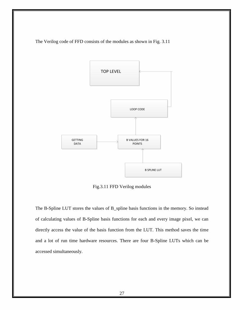
The Verilog code of FFD consists of the modules as shown in Fig. 3.11
B SPLINE LUT
TOP LEVEL
LOOP CODE
GETTING DATA
B VALUES FOR 16 POINTS
Fig.3.11 FFD Verilog modules
The B-Spline LUT stores the values of B_spline basis functions in the memory. So instead
of calculating values of B-Spline basis functions for each and every image pixel, we can
directly access the value of the basis function from the LUT. This method saves the time
and a lot of run time hardware resources. There are four B-Spline LUTs which can be
accessed simultaneously.

28
The figure below shows how B-Spline LUT is implemented in hardware
Fig. 3.12 B-Spline LUT

29
The second module “calculating B-Spline for the 16 points” gets the values of B-Splines
from the LUTs in the memory. These values are then assigned to respective B’s on the
basis of the input values of the image pixels.
The hardware implementation of this module is shown in fig. 3.13
Fig. 3.13 Calculating B for 16 input pixels
The module getting data reads the image file (gray scale) saved as text file in the memory
and assigns the respective values to the control points and the data points.

30
The image contents of the memory as displayed in Xilinx are shown in Fig. 3.14.
Fig.3.14 memory contents of the image file
The “loop code” calculates the effect of CPs on the image pixels on the basis of B-Spline
values. The hardware implementation of loop code is shown below.

31
Fig.3.15 Loop Code
32
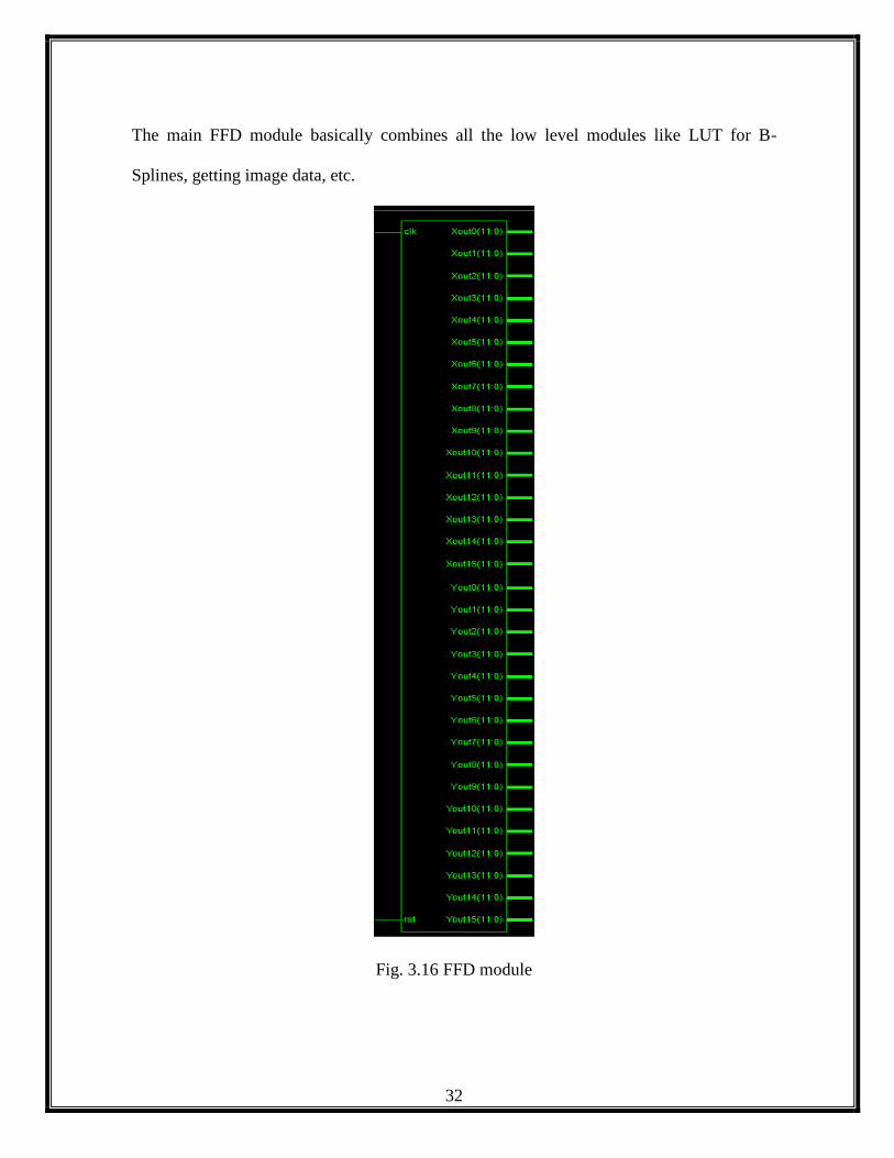
The main FFD module basically combines all the low level modules like LUT for B-
Splines, getting image data, etc.
Fig. 3.16 FFD module

33
Fig.3.17 FFD module another view

34
The simulation diagram for the FFD shows the signals for clk and rst both are operated on
positive edge. X0-X16and Y0-Y16 shows the 16 grey points of the image which have
undergone the whole process of FFD. The input data is taken directly from the text file
(containing pixelsof the image) from the memory.
Fig. 3.18Simulation diagram for FFD

35
3.3 Implementation of FFD on NoC
The basic architecture of the PNoC for the B-Spline based architecture is shown in Fig.
3.14. There are total 16 control points for each grid of image pixels. The central 8 pixels
are fed into block 1A and the effect of control point (1-4) is calculated on these pixels. The
other 8 central pixels are fed into the block 1B and the effect of CP1-CP4 is calculated.
Fig. 3.19PNoC architecture for FFD

36
The first 8 central pixels from the block 1A are fed into block 2A and effect of CP5-8 is
calculated on them. Similarly, pixels from 1B are fed into 2B for the calculation of effect of
CP5-8. The effect of all the 16 control points on these pixels is calculated. All these steps
are repeated until all the pixels in the image are processed.
The coordination of the image data transfer between different nodes is the main design
challenge of the system. There are two major communications. The first one involves the
CPU to communicate with the block processors and the second one is between different
block modules.
PNoC is very well suitable for this system as more than one connection are active at any
instant so inter-block data transfer can occur simultaneously. The choice of window to be
chosen is made by the router and no extra hardware is required for that, and, if no module
is available the connection request can be queued up until the availability of a block. As
this system is flexible so additional blocks can be added to the present design as well.
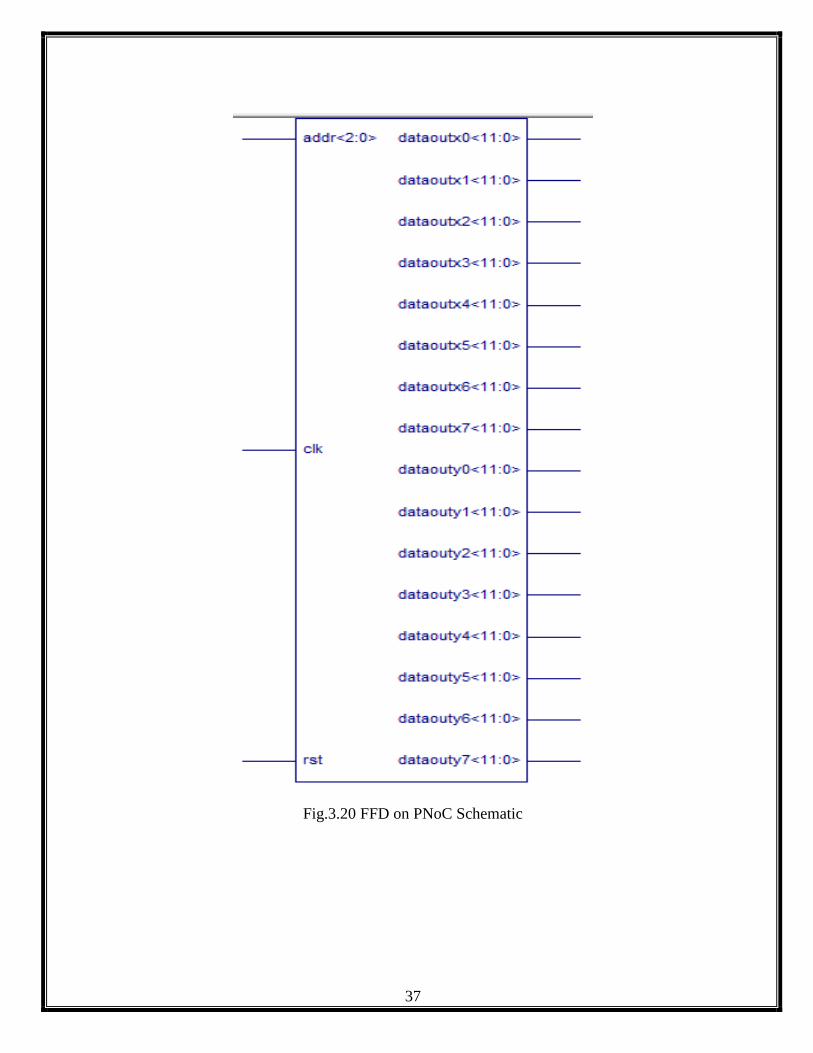
The top level implementation schematic for the FFD on PNoC is shown
37
Fig.3.20 FFD on PNoC Schematic
38
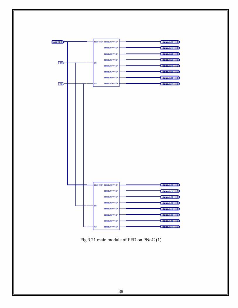
Fig.3.21 main module of FFD on PNoC (1)
39
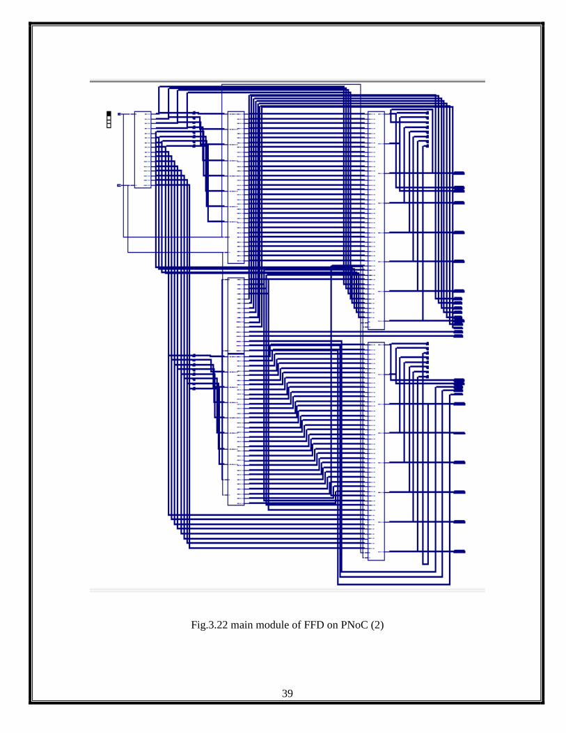
Fig.3.22 main module of FFD on PNoC (2)

40
Fig.3.23 main module of FFD on PNoC (3)

41
The simulation diagrams for the final implementation are shown below. The simulation
diagram shows the signals for clk and rst both are operated on positive edge. dataoutx0-
dataoutx15 and dataouty0-dataouty15 shows the 16 grey points of the image which have
undergone the whole process of FFD. The input data is taken directly from the text file
(containing pixels of the image) from the memory. The addrvalue showsthe position of the
pixel in the given node.
Fig.3.24 value of output pixels for first 310ns

42
Fig.3.25 Values of pixels from 520-630ns

43
Fig.3.26 Values of pixels from 670-790ns

44
Chapter # 4
Results and Discussion

45
Chapter # 4 Results and Discussion
The figure 4.1 shows the simulation report of the NoC architecture module
Fig. 4.1 Xilinx simulation report for NoC
Table 1 shows the comparison of Hilton and Nelson’s and the proposed NoC
implementations. The setup was designed to exhibit maximum data transfer ability. The
same device and port and data widths were used. We got similar results for both
implementations in spite of different languages used for implementing the architectures.

46
Table 1. Comparison of different NoC architectures
Table 2 shows the advantage of using PNoC over conventional architectures. Although
PNoC requires more hardware resources as compared to shared and locked bus, but its
efficiency is more in terms of speed and timing. The circuit switched NoC is better in area
and speed as compared to packet switched network.

47
Table 2. Comparison of PNoC with existing architectures
The figure 4.2 shows the timing report for the FFD architecture
Fig. 4.2 Simulation report for FFD
48
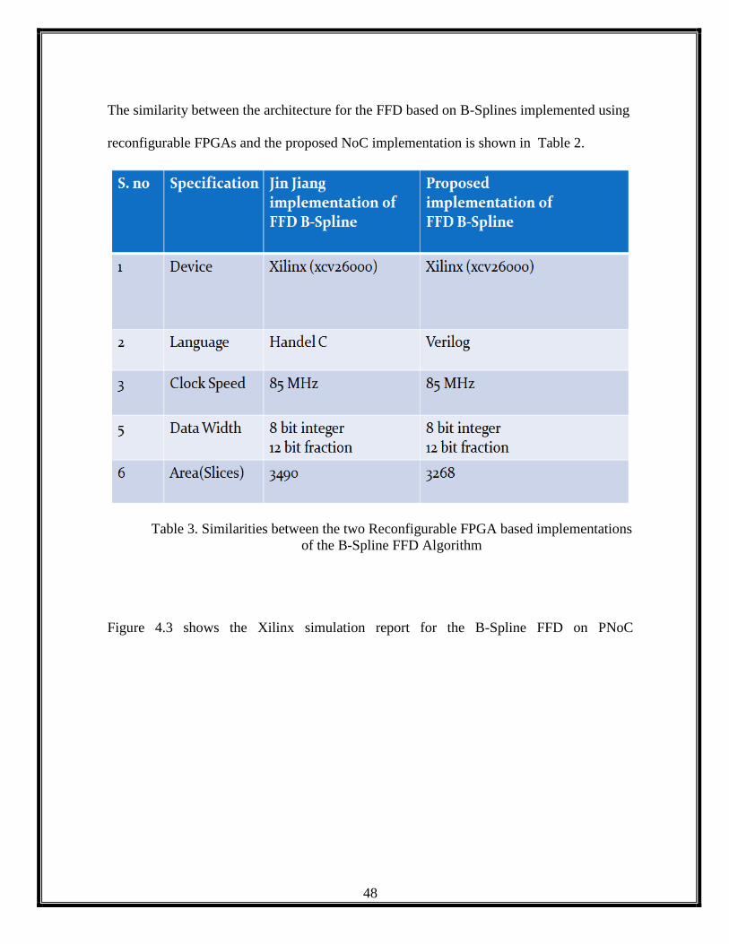
The similarity between the architecture for the FFD based on B-Splines implemented using
reconfigurable FPGAs and the proposed NoC implementation is shown in Table 2.
Table 3. Similarities between the two Reconfigurable FPGA based implementations
of the B-Spline FFD Algorithm
Figure 4.3 shows the Xilinx simulation report for the B-Spline FFD on PNoC

49
Figure 4.3 Xilinx simulation report for FFD on PNoC
The final design for FFD on PNoC is implemented on XC2v6000 device. Table 3 shows
the comparison of different hardware implementations of the FFD algorithm. The clock
speed of the proposed design is approximately 67MHz and the execution time is recorded
to be as 60ms. The area is increased as compared to the Reconfigurable FPGA based
implementation by Jiang [7]. However, the proposed implementation provides the best
performance as illustrated by the throughput in terms of pixels/seconds as shown in Table
3. The throughput was better than all the other FFD implementations for 2D images. The
clock speed and execution time was a little slow as compared to other implementations;
this may be due to the increase in the area.

50
Table 4. Comparing different FFD hardwares for the 2D images for size of 256 x 256

51
Chapter # 5
Conclusion and Future
Work Conclusion
Future Work

52
Chapter 5 Conclusion and Future Work
5.1 Conclusion
As the system complexity increases, the bus based communication systems are not efficient
in terms of scalability, and design and verification times. Moreover, the demand for higher
computational speeds and lower power consumption is essentially required in most of the
consumer electronics and medical equipment. The NoC technology provides a possible
solution to all these problems.
The NoC technology tends to provide high performance and low power consumption for
system-on-chip architectures. NoCs have been implemented in different configurations and
provide various capabilities.
The B-Spline based FFD algorithm is considered to be one of the most powerful techniques
for modeling 3-D deformable objects in the domain of non-rigid image registration, which
is a special kind of image registration used specifically for images with nonlinear geometric
differences. The main motivation behind the optimization of this algorithm in the current
thesis is the increasing utilization of non-rigid registration for the analysis of brain images
and thus an associated enormous performance requirement to be able to analyze huge and
complex brain images.
The thesis describes a NoC based implementation of the B-Spline FFD algorithm. For this
purpose, we used PNoC, which is a very flexible architecture that suits the FPGA-based
systems. Our design description is captured in Verilog language and implemented on
53
Xilinx XC2V6000 device at 37 MHz. The proposed design is parametrizable at the compile
time for the computational precisions and to support a range of image resolutions. The
experimental results have shown a significant improvement in performance when
compared with the other hardware implementations of the B-Spline FFD Algorithm.
5.2 Future Work
To the best of our knowledge, this is the first implementation of a medical registration
algorithm that is based on NoC. Our promising results illustrate the usefulness of NoC in
the medical registration algorithms and thus other algorithms, such as non-rigid registration
for breast MR images, PETCT image registration in the chest, can also be implemented
using our generic PNoC model. Another interesting future extension is to partition the
images into 3 by 3 sub-images and then use 9 pipelined processors for a single block in
parallel for each one of the sub-image that contains 12-bit fixed-point data. The slice
resources for this system would be around 31410 for each block and it would allow us to
further enhance the performance.

54
References:
[1] Y.-C. Tai, K. P. Lin, C. K. Hoh, S. C. H. Huang, and E. J. Hoffman, "Utilization of 3-D
elastic transformation in the registration of chest X-ray CT and whole body PET," IEEE
Transactions on Nuclear Science, volume 44, pgs.1606-1612, 1997.
[2] ] D. Mattes, D. R. Haynor, H. Vesselle, T. K. Lewellen, and W. Eubank, "PETCT
image registration in the chest using free-form deformations," IEEE Transactions on
Medical Imaging, volume22, pgs. 120-128, 2003.
[3] M. R. Kaus, T. Netsch, S. Kabus, V. Pekar, T. McNutt, and B. Fischer,"Estimation of
organ motion from 4D CT for 4D radiation therapy planning of lung cancer," in Lecture
Notes in Computer Science, vol. 3217: Springer-Verlag GmbH, 2004, pgs. 1017-1024.
[4] G. C. Sharp, S. B. Jiang, S. Shimizu, and H. Shirato, "Prediction of respiratory tumour
motion for real-time image-guided radiotherapy," Physics in Medicine & Biology,
volume49, pgs. 425-440, 2004.
[5] Rueckert D, Aljabar P, Heckemann RA, Hajnal JV, Hammers “Diffeomorphic
Registration using B-Splines”. MICCAI.;4191:702–709, 2006.

55
[6] D. Rueckert,* L. I. Sonoda, C. Hayes, D. L. G. Hill, M. O. Leach, and D. J. Hawkes
“Nonrigid registration using free-Form deformations: application to breast MR
images,” IEEE Transactions on Medical Imaging, volume18, pgs. 8, 2009.
[7] J. Jiang, W. Luk and D. Rueckert, “FPGA-based computation of free-form
deformations in medical image registration,” ,” IEEE International Conference on
Field-Programmable Technology, pgs. 407-410, 2002.
[8] C. Berthaud, E. Bourennane, M. Paindavoine and C. Milan, “Implementation of a real
time image rotation using B-Spline interpolation On FPGA’s Board,”International
Conference on Image Processing, pgs. 995-999,1998.
[9] J. Jiang, W. Luk and D. Rueckert, “An FPGA-based Computation of Free-Form
Deformations”, In Field-Programmable Logic and Applications, Lecture Notes in
Computer Science, pages 1057 – 1061, 2003.
[10] D. Bertozzi and L. Benini, “Xpipes: A network-on-chip architecture for gigascale
systems-on-chip”, IEEE Circuits and Systems Magazine, volume4, Issue 2, pgs. 18-31,
2004.

56
[11] A.Agarwal and R. Shankar, “A layered architecture for NOC design methodology”,
IASTED International Conference on Parallel and Distributed Computing and Systems,
pgs. 659-666, 2005.
[12]L. Benini and G. De Micheli, “ Networks on Chip: a New SoC Paradigm”, IEEE
Computer, volume1, pgs. 70–78, 2002.
[13] C.Hilton and B. Nelson, PNoC: “A flexible circuit-switched NoC for FPGA-based
systems,” IEEE proceedings computers and digital techniques, volume153 Issue 3,
2006.
[14]E. Salminen, V. Lahtinen, K. Kuusilinna, and T. Hamalainen, “Overview of bus-based
system-on-chip interconnections,” in Proceedings of the IEEE International Symposium
on Circuits and Systems. ISCAS 02, , pgs. 372–375 vol.2, 2002.
[15] Hutchings, B., Bellows, P., Hawkins, J., Hemmert, S., Nelson, B., and Rytting, M.,
“A CAD suite for high-performance FPGA design”, in Pocek, K.L., and Arnold, J.M.
(Eds.). Proc. IEEE Workshop on FPGAs for Custom Computing Machines, Napa, CA,
USA, pgs. 175-184, 1999, (IEEE Computer Society).
[16]J. Dally and B. Towles Principles and Practices of Interconnection Networks, Morgan
Kaufmann, 2004.

57
[17]A. Ivanov, C. Grecu, M. Jones, P. PratimPande, and R. Saleh, P. PratimPande, C.
Grecu, M. Jones, A. Ivanov, and R. Saleh, “Performance evaluation and design trade-
offs for network-on-chip interconnect architectures”,IEEE Transactions on Computers,
volume54, no. 8, pgs. 1025-1040, 2005.
[18]A. Adriahantenaina, H. Charlery, A. Greiner, L. Mortiez, and C.A. Zeferino, article
“SPIN: a scalable, packet switched,on-chip micro-network”, The Proc. IEEE
Conference on Design, Automation and Test, pgs. 70-73, 2003.
[19]J. W. Dally and B. Towles, “Route packets, not wires: article ”On-Chip
interconnection networks”, The Proc. IEEE International Conference on Design and
Automation, pgs. 684-689,2001.
[20]P. T. Wolkotte, G. J. M. Smit, G. K. Rauwerda, and L. T. Smit, article “An energy-
efficient reconfigurable circuitswitched network-on-chip”, The Proc. 19th IEEE
International Conference on Parallel and Distributed Processing Symposium, pgs. 155-
163, 2005.

58
[21]M. Millberg, E. Nilsson, R. Thid, S. Kumar, and A. Jantsch.article “The Nostrum
backbone - A communication protocol stack for networks on chip”, The Proc. IEEE
International Conference on VLSI Design, pgs. 693, 2004.
[22] K. M. Al-Tawil, M. Abd-El-Barr, and F. Ashraf, article “A survey and comparison
of wormhole routing techniques in mesh networks”, The IEEE Network, volume11,
pgs. 38–45, 1997.
[23] ARTERIS. A comparison of network-on-chip and buses.Whitepaper,2005.
http://www.arteris.com/nocwhitepaper.pdf.
[24] T. Bjerregaard and J. Sparsø, article “A router architecture for connection-oriented
service guarantees in the MANGO clockless Network-on-Chip”, The Proc. Of IEEE on
Design Automation and Test, volume2, pgs. 1226-1231, 2005.
[25] E. Bolotin, I. Cidon, R. Ginosar, and A. Kolodny,article “QNoC: QoS architecture
and design process for network on chip”, The Journal of Systems Architecture, Volume
50, Issue 2-3 (Special Issue on Network on Chip), pgs. 105-128,2004.
[26] S. Kumar, A. Jantsch, J-P. Soininen, M. Forsell, M. Millberg, J. Oberg, K. Tiensyrja,
and A. Hemani, article“A network on chip architecture and design methodology”, The
IEEE Computer, pgs. 117-124, 2002.
59
[27] E. Rijpkema, K. Goossens, A. Radulescu, J. Dielissen, J. van Meerbergen, P.
Wielage, and E. Waterlander, article “Trade-offs in the design of a router with both
guaranteed and best-effort services for networks on chip”,The IEE Proc. on Computers
and Digital Techniques, volume150, Issue 5, pgs. 294-302, 2003.
[28] K. Goossens, J. Dielissen, and A. Radulescu,article “A Ethereal network on chip:
Concepts, architectures, and implementations”, TheIEEE Design & Test of Computers,
volume22, Issue 5, pgs. 414-421,2005.
[29] A. Siebenborn, O. Bringmann, and W. Rosenstiel, article “Communication analysis
for network-on-chip design”,The Proc. IEEE International conference on Parallel
Computing in Electrical Engineering, pgs. 315-320, 2004.
[30] C. Neeb, M. Thul, and N. Andwehn,article “Network on-chip-centric approach to
interleaving in high throughput channel decoders”, The Proc. IEEE International
Symposium on Circuits and Systems, pgs. 1766–1769, 2005.

60
Appendix1:
Affine Transformation
3-D affine transformation is written as
in above equation are the global transformation parameters and shows the 12 degrees of
freedom.
Affine transformations consists of rotation,scaling, and shearing
For 2-D case
in above equation are the global transformation parameters and shows the 6 degrees of
freedom.
Rotation Matrix
Scaling Matrix
Shear Matrix
Now if rotation is – then and scaling is with no shear then
61
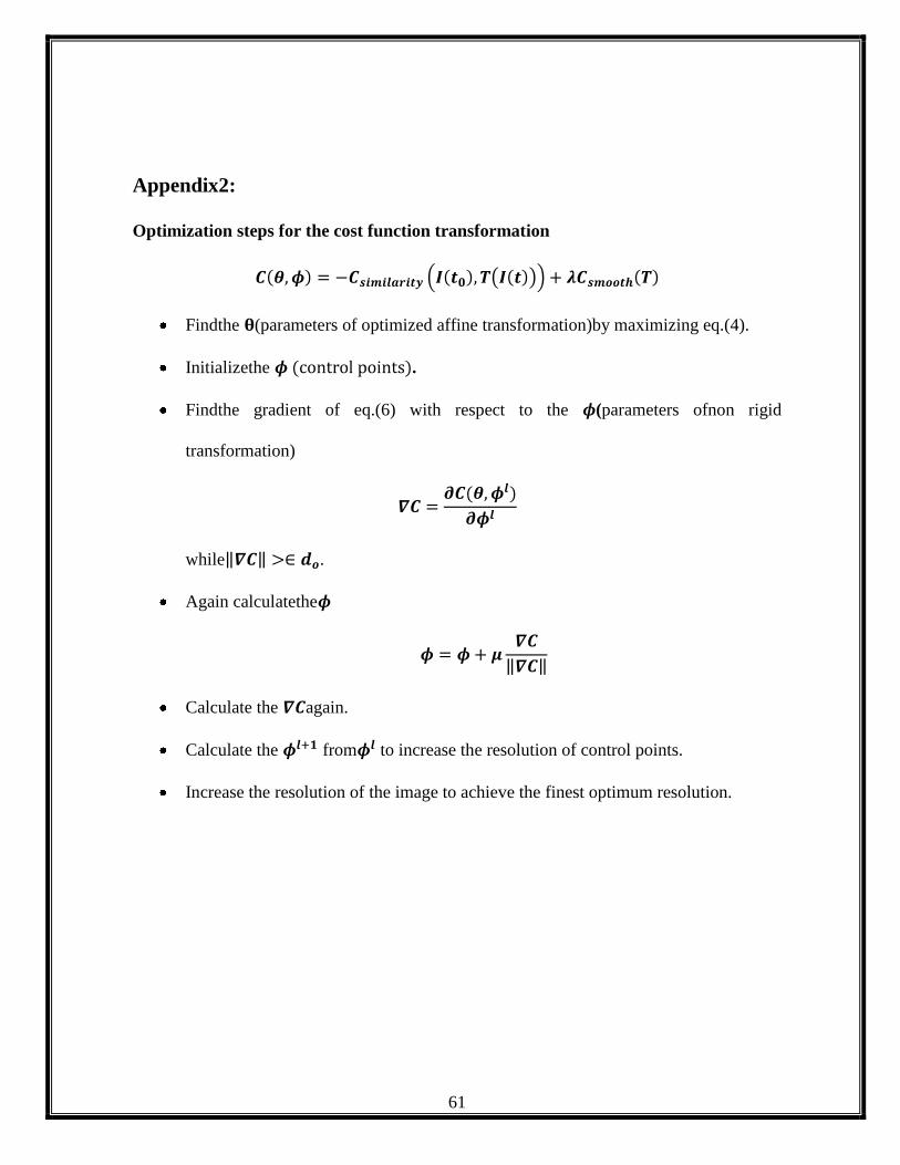
Appendix2:
Optimization steps for the cost function transformation
Findthe (parameters of optimized affine transformation)by maximizing eq.(4).
Initializethe .
Findthe gradient of eq.(6) with respect to the (parameters ofnon rigid
transformation)
while .
Again calculatethe
Calculate the again.
Calculate the from to increase the resolution of control points.
Increase the resolution of the image to achieve the finest optimum resolution.