design of the nios ii system for the playing of wave files ...ijetch.org/papers/576-t911.pdf · hdl...
TRANSCRIPT

Abstract—The motivation behind this study is the impact
made on today’s social media by music players, which include features like portability, size and equalizer functionality for the best possible sound output quality. The objective of this study was to develop a system that reads the wave files present on the Secure Data (SD) card, adjust the equalizer settings incorporated on it, and play them on the speaker with the best possible quality sound output. This was done with the help of the SD card slot provided on the DE2 board, and its implementation on the board using Altera’s SoPC (System-on-a-Programmable-Chip) Builder in the Altera Quartus 9.1 environment. Nios II is a 32-bit soft-core embedded processor architecture designed specifically for the Altera family of FPGAs. Programming of the Nios II processor is done using the Nios II 9.1 IDE tool. An extension of this work could include incorporation of video—along with the audio on the DE2 board since there is a VGA slot included on the board features and the movement of the wave files on the SD card with the help of the keys present on the DE2 board.
Index Terms—Embedded processor, Nios II embedded design, SoPC builder, and system on a programmable chip builder.
I. INTRODUCTION Indicative of the popularity of being able to read wave
files on SD (secure data) cards, there is no shortage of entries in the literature, on blogs and discussion boards, and postings of schematics. In this study, though, the authors address design advancements of the DE2_SD audio board in accordance with conceptual design methods [1-8] offering extended user control with features such as pause, reset and start, and—with the implementation of switches—an equalizer. The objective of this study was to develop a system that reads the wave files present on the SD card and plays them on the speaker with the best possible quality sound output.
This was done with the help of the SD card slot provided on the DE2 board and its implementation on the board using Altera’s SoPC (System-on-a-Programmable-Chip) Builder in the Altera Quartus 9.1 environment. Other increases in functionality include the resetting of songs to the start of the
Manuscript received November 20, 2012; revised April 8, 2013. S. Moslehpour is with the College of Engineering, Technology, and Ar-
chitecture at Hartford University, Hartford, CT, USA (e-mail: [email protected]).
K. Jenab is with the Socitey of Reliability Engineering-Ottawa Chapter, Ottawa, Ontario, Canada (e-mail: [email protected]).
P. D. Weinsier is EEET Program Director at the Bowling Green State University-Firelands, USA (e-mail: [email protected]).
B. K. Matcha was with the College of Engineering, Technology, and Architecture at Hartford University, Hartford, CT, USA (e-mail: [email protected]).
playlist. As an example, red and green LEDs on the DE2 board are
controlled by the frequency of the music. Advanced features include an LCD display to provide feedback to the user not the least of which is a welcome message when the board is programmed which is important as user functionality increases.
A. SoPC Builder Sensor network research began, like many of today’s
technological advances, with the military in such applications as battle-field surveillance and enemy tracking [9]. After the technology proved itself, it quickly spread to civilian applications such as data centers, industrial settings and environmental observation and forecasting. However, due to non-standard communications protocols and electrical properties, sensor networks tend to be expensive, in spite of their broad use for Internet Protocol (IP) and platforms such as Hyper Text Transfer Protocol (HTTP), Simple Mail Transfer Protocol (SMTP) and Simple Network Management Protocol (SNMP) [10].
As chip technology has advanced to Ultra Large-Scale Integration (ULSI) and Giga-Scale Integration (GSI), System-on-a-single-Chip (SoC) technology has brought prices way down. Adding programmability to these devices, a System-on-a-Programmable-Chip (SoPC) can be designed right onto high-density devices such as Field Programmable Gate Arrays (FPGAs), thereby offering flexibility to embedded systems design [11]. Now, SoC designs are moving from single-processor-based systems toward the integration of multi-processor architectures on a single chip (MPSoCs), due to intensive data communication requirements [12].
SoPC is a new technology which has emerged that enables designers to utilize a large FPGA that contains memory blocks, interface blocks, logic elements and analog blocks [13]. These blocks, along with an intellectual property (IP) processor core, can be combined on a single chip in order to target a specific application. Designers use SoPC for creating an FPGA which is composed of memory blocks, interface blocks, logic elements and analog blocks [14]. These blocks, along with an intellectual property (IP) processor core, can be combined on a single chip in order to target a specific application, thereby offering the user a very powerful system development tool. SoPC Builder [15] is a general-purpose tool that has the advantage of faster development times over manual integration methods [16] and is part of the Altera’s Quartus II software.
There is no doubt that some designers still prefer to manually program and wire each piece of a given system. For most, though, the preference is to move beyond writing
Design of the Nios II System for the Playing of Wave Files on an Altera DE2 Board
S. Moslehpour, K. Jenab, Sr. Member, IEEE, P. D. Weinsier, and B. K. Matcha
IACSIT International Journal of Engineering and Technology, Vol. 5, No. 3, June 2013
361DOI: 10.7763/IJET.2013.V5.576
HDL (Hardware Description Language) modules by hand. For them, SoPC Builder makes system design easier by allowing them to simply specify a component in a GUI from which Builder automatically provides the logical interconnects. Furthermore, Builder is capable of delivering Verilog HDL or VHDL designs, affording yet more flexibility to designers, who prefer one over the other.
B. Nios II Processor The Nios II processor is a configurable soft-core
processor that allows features to be added or removed on a system-by-system basis to meet performance requirements. Users can configure the Nios II processor and add peripherals to meet their specifications, and then program the system into an Altera FPGA. On this single Altera chip or Nios II processor core the user can implement both peripherals and memory (both on- and off-chip). Such a system is similar to a microcontroller or computer on a chip having a CPU.
C. SoPC Design Flow While there are CAD tools available commercially, which
are available to the user for either their HDL or schematic design entry methods, manufacturers of FPGAs such as Altera (Quartus II) and Xilinx (ISE) provide such tools through their own software packages. These tools actually help step the designer through the process as follows:
• Package your component for SoPC Builder using the
Component Editor • Simulate at the unit-level, possibly incorporating
Avalon BFMs (Bus Functional Models) to verify the system
• Complete the SoPC Builder design by adding other components, specifying interrupts, clocks, resets, and addresses
• Generate the SoPC Builder system • Perform system-level simulation • Constrain and compile the design • Download the design to an Altera device • Test the design on the hardware
A major consideration here is that designers can still choose to develop their designs in the traditional piecemeal way, or move forward and allow more user-friendly software programs to do the leading, thus allowing the design more time to, well, design. As noted earlier, SoPC Builder provides a tool block to customize the configuration of a processor-core for a given application via a GUI interface with configurable parameters such as data-path width, memory and address space. A number of peripherals are also configurable and include UARTs, general-purpose I/O, Ethernet and memory controllers. After the parameters are chosen and the GUI interface completed, the HDL or net-list file and a number of other library files are generated relative to the new processor core being generated. Using standard files from SoPC Builder [17], the design is then compiled onto an FPGA. Subsequent programming of the design onto the processor is accomplished via a C/C++ compiler.
The final step, then, is to load the new program file into the program and data memories of the processor. This can be accomplished in a multitude of ways, dependent on the processor’s memory configuration. In general, processor cores are classified as either hard or soft [18]. The designa-tion of a core being either hard or soft refers to its flexibility or ability to be configured. That is, hard cores generally have the advantage of higher performance characteristics but at the cost of configurability. Soft cores use existing pro-grammable logic elements from the FPGA to implement the processor logic. Soft cores have the advantage in flexibility additional features, more ALU functionality, adjustable memory width, and user-specified peripherals and memory address space but at the cost of higher power and slower clock speeds [19].
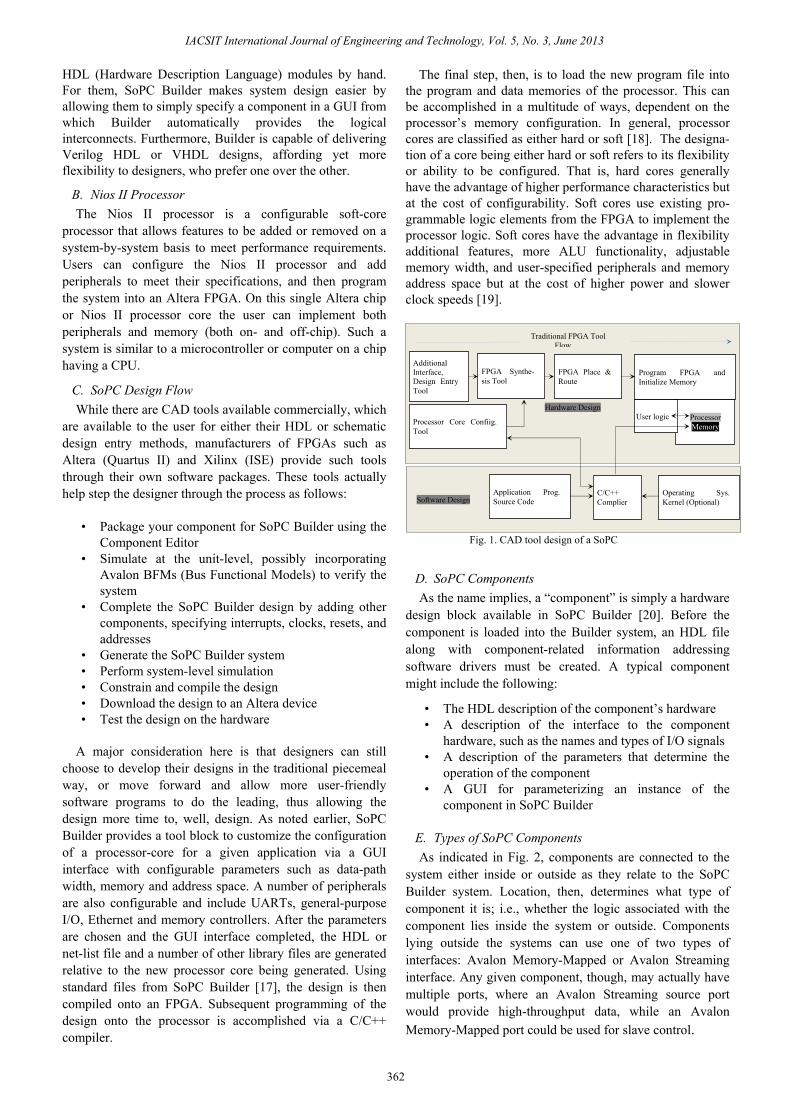
Fig. 1. CAD tool design of a SoPC
D. SoPC Components As the name implies, a “component” is simply a hardware
design block available in SoPC Builder [20]. Before the component is loaded into the Builder system, an HDL file along with component-related information addressing software drivers must be created. A typical component might include the following:
• The HDL description of the component’s hardware • A description of the interface to the component
hardware, such as the names and types of I/O signals • A description of the parameters that determine the
operation of the component • A GUI for parameterizing an instance of the
component in SoPC Builder
E. Types of SoPC Components As indicated in Fig. 2, components are connected to the
system either inside or outside as they relate to the SoPC Builder system. Location, then, determines what type of component it is; i.e., whether the logic associated with the component lies inside the system or outside. Components lying outside the systems can use one of two types of interfaces: Avalon Memory-Mapped or Avalon Streaming interface. Any given component, though, may actually have multiple ports, where an Avalon Streaming source port would provide high-throughput data, while an Avalon Memory-Mapped port could be used for slave control.
Software Design
Hardware Design
Additional Interface, Design Entry Tool
FPGA Synthe-sis Tool
FPGA Place & Route
Program FPGA and Initialize Memory
Processor Memory
User logic Processor Core Confiig. Tool
Traditional FPGA Tool Flow
Application Prog. Source Code
C/C++ Complier
Operating Sys. Kernel (Optional)
IACSIT International Journal of Engineering and Technology, Vol. 5, No. 3, June 2013
362

Fig. 2. System components
F. Avalon Switch Interconnect Taken together, the resources for connecting Avalon
master and slaves on a system component represent the system interconnect fabric. Details of the connection are,
then, addressed by SoPC Builder as it attempts to match them with the system interconnect fabric. The job of the interconnect fabric is to ensure that signals are correctly routed between master and slaves. The following items are supported by memory-mapped interfaces, noting that there can be almost any combination in the number of masters and slaves.
• Any number of master and slave components • On-chip components • Interfaces to off-chip devices • Master and slaves of different data widths • Components operating in different clock domains • Components using multiple Avalon-MM ports
In cases requiring more complex interfaces than a single
Avalon Memory-Mapped interface, SoPC Builder is capable and, in fact, is its primary purpose [7] of creating and connecting components with system interconnect fabrics for multiple interfaces (see Fig. 3), given that they conform to Avalon Interface Specifications.
Fig. 3. System interconnect fabric
G. Address Decoding The logic in charge of address decoding forwards the
appropriate addresses from master to slave through the system interconnects fabric. It is not necessary, however, for slaves to decode addresses, as long as they are properly aligned to the interface. It should be noted that manual edits of the HDL file are not necessary in order to modify the system’s memory map. Fig. 4 offers an example of how address decoding is accomplished for one master and two slaves. Fig. 5 shows an example of how each master in the system is assigned its own decoding logic. The job of this logic is to coordinate the difference in address widths
between the master and each slave.
Fig. 4. Address decoding logic
IACSIT International Journal of Engineering and Technology, Vol. 5, No. 3, June 2013
363
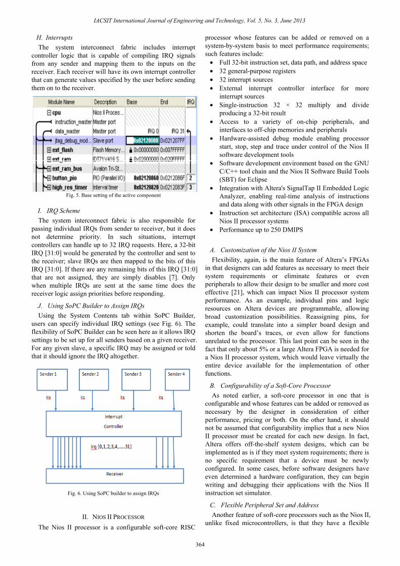
H. Interrupts The system interconnect fabric includes interrupt
controller logic that is capable of compiling IRQ signals from any sender and mapping them to the inputs on the receiver. Each receiver will have its own interrupt controller that can generate values specified by the user before sending them on to the receiver.
Fig. 5. Base setting of the active component
I. IRQ Scheme The system interconnect fabric is also responsible for
passing individual IRQs from sender to receiver, but it does not determine priority. In such situations, interrupt controllers can handle up to 32 IRQ requests. Here, a 32-bit IRQ [31:0] would be generated by the controller and sent to the receiver; slave IRQs are then mapped to the bits of this IRQ [31:0]. If there are any remaining bits of this IRQ [31:0] that are not assigned, they are simply disables [7]. Only when multiple IRQs are sent at the same time does the receiver logic assign priorities before responding.
J. Using SoPC Builder to Assign IRQs Using the System Contents tab within SoPC Builder,
users can specify individual IRQ settings (see Fig. 6). The flexibility of SoPC Builder can be seen here as it allows IRQ settings to be set up for all senders based on a given receiver. For any given slave, a specific IRQ may be assigned or told that it should ignore the IRQ altogether.
Fig. 6. Using SoPC builder to assign IRQs
II. NIOS II PROCESSOR The Nios II processor is a configurable soft-core RISC
processor whose features can be added or removed on a system-by-system basis to meet performance requirements; such features include:
• Full 32-bit instruction set, data path, and address space • 32 general-purpose registers • 32 interrupt sources • External interrupt controller interface for more
interrupt sources • Single-instruction 32 × 32 multiply and divide
producing a 32-bit result • Access to a variety of on-chip peripherals, and
interfaces to off-chip memories and peripherals • Hardware-assisted debug module enabling processor
start, stop, step and trace under control of the Nios II software development tools
• Software development environment based on the GNU C/C++ tool chain and the Nios II Software Build Tools (SBT) for Eclipse
• Integration with Altera's SignalTap II Embedded Logic Analyzer, enabling real-time analysis of instructions and data along with other signals in the FPGA design
• Instruction set architecture (ISA) compatible across all Nios II processor systems
• Performance up to 250 DMIPS
A. Customization of the Nios II System Flexibility, again, is the main feature of Altera’s FPGAs
in that designers can add features as necessary to meet their system requirements or eliminate features or even peripherals to allow their design to be smaller and more cost effective [21], which can impact Nios II processor system performance. As an example, individual pins and logic resources on Altera devices are programmable, allowing broad customization possibilities. Reassigning pins, for example, could translate into a simpler board design and shorten the board’s traces, or even allow for functions unrelated to the processor. This last point can be seen in the fact that only about 5% or a large Altera FPGA is needed for a Nios II processor system, which would leave virtually the entire device available for the implementation of other functions.
B. Configurability of a Soft-Core Processor As noted earlier, a soft-core processor in one that is
configurable and whose features can be added or removed as necessary by the designer in consideration of either performance, pricing or both. On the other hand, it should not be assumed that configurability implies that a new Nios II processor must be created for each new design. In fact, Altera offers off-the-shelf system designs, which can be implemented as is if they meet system requirements; there is no specific requirement that a device must be newly configured. In some cases, before software designers have even determined a hardware configuration, they can begin writing and debugging their applications with the Nios II instruction set simulator.
C. Flexible Peripheral Set and Address Another feature of soft-core processors such as the Nios II,
unlike fixed microcontrollers, is that they have a flexible
IACSIT International Journal of Engineering and Technology, Vol. 5, No. 3, June 2013
364
peripheral set. This flexible peripheral set allows designers to target each system to a specific application [7] with software constructs. These are used to generically independent of address location—access both memory and peripherals. The fact that a flexible address map comes from having a flexible peripheral set is not lost of the designer as it has no effect on application developers. Peripherals can be
classified as either standard peripherals or custom peripherals.
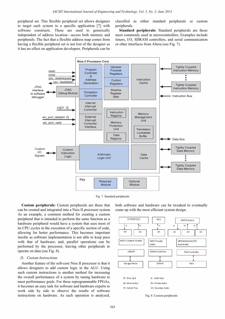
Standard peripherals: Standard peripherals are those most commonly used in microcontrollers. Examples include timers, I/O, SDRAM controllers, and serial communication or other interfaces from Altera (see Fig. 7).
Fig. 7. Standard peripherals
Custom peripherals: Custom peripherals are those that
can be created and integrated into a Nios II processor system. As an example, a common method for creating a custom peripheral that is intended to perform the same function as a hardware peripheral would have a system that uses most of its CPU cycles in the execution of a specific section of code, allowing for better performance. This becomes important insofar as software implementation is not able to keep pace with that of hardware; and, parallel operations can be performed by the processor, leaving other peripherals to operate on data (see Fig. 8).
D. Custom Instructions Another feature of the soft-core Nios II processor is that it
allows designers to add custom logic in the ALU. Using such custom instructions is another method for increasing the overall performance of a system by tuning hardware to meet performance goals. For these reprogrammable FPGAs, it becomes an easy task for software and hardware experts to work side by side to observe the results of software instructions on hardware. As each operation is analyzed,
both software and hardware can be tweaked to eventually come up with the most efficient system design.
Fig. 8. Custom peripherals
IACSIT International Journal of Engineering and Technology, Vol. 5, No. 3, June 2013
365
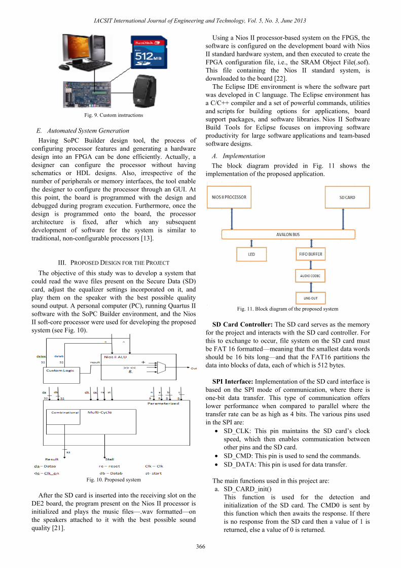
Fig. 9. Custom instructions
E. Automated System Generation Having SoPC Builder design tool, the process of
configuring processor features and generating a hardware design into an FPGA can be done efficiently. Actually, a designer can configure the processor without having schematics or HDL designs. Also, irrespective of the number of peripherals or memory interfaces, the tool enable the designer to configure the processor through an GUI. At this point, the board is programmed with the design and debugged during program execution. Furthermore, once the design is programmed onto the board, the processor architecture is fixed, after which any subsequent development of software for the system is similar to traditional, non-configurable processors [13].
III. PROPOSED DESIGN FOR THE PROJECT The objective of this study was to develop a system that
could read the wave files present on the Secure Data (SD) card, adjust the equalizer settings incorporated on it, and play them on the speaker with the best possible quality sound output. A personal computer (PC), running Quartus II software with the SoPC Builder environment, and the Nios II soft-core processor were used for developing the proposed system (see Fig. 10).
Fig. 10. Proposed system
After the SD card is inserted into the receiving slot on the
DE2 board, the program present on the Nios II processor is initialized and plays the music files—.wav formatted—on the speakers attached to it with the best possible sound quality [21].
Using a Nios II processor-based system on the FPGS, the software is configured on the development board with Nios II standard hardware system, and then executed to create the FPGA configuration file, i.e., the SRAM Object File(.sof). This file containing the Nios II standard system, is downloaded to the board [22].
The Eclipse IDE environment is where the software part was developed in C language. The Eclipse environment has a C/C++ compiler and a set of powerful commands, utilities and scripts for building options for applications, board support packages, and software libraries. Nios II Software Build Tools for Eclipse focuses on improving software productivity for large software applications and team-based software designs.
A. Implementation The block diagram provided in Fig. 11 shows the
implementation of the proposed application.
Fig. 11. Block diagram of the proposed system
SD Card Controller: The SD card serves as the memory
for the project and interacts with the SD card controller. For this to exchange to occur, file system on the SD card must be FAT 16 formatted—meaning that the smallest data words should be 16 bits long—and that the FAT16 partitions the data into blocks of data, each of which is 512 bytes.
SPI Interface: Implementation of the SD card interface is based on the SPI mode of communication, where there is one-bit data transfer. This type of communication offers lower performance when compared to parallel where the transfer rate can be as high as 4 bits. The various pins used in the SPI are:
• SD_CLK: This pin maintains the SD card’s clock speed, which then enables communication between other pins and the SD card.
• SD_CMD: This pin is used to send the commands. • SD_DATA: This pin is used for data transfer.
The main functions used in this project are: a. SD_CARD_init()
This function is used for the detection and initialization of the SD card. The CMD0 is sent by this function which then awaits the response. If there is no response from the SD card then a value of 1 is returned, else a value of 0 is returned.
IACSIT International Journal of Engineering and Technology, Vol. 5, No. 3, June 2013
366

b. SD_read_lba() This function allows multiple blocks to be read from the SD card after which the CMD17 represents the READ command. Next, lba value—representing specific locations on the SD card—reads each byte individually from the SD card location.
Audio Codec: Audio Codec—located between the Buffer
and the Line-Out—is the part of the system where digital-to-analog conversion (DAC) takes place in order for the music to play on the speakers [23]. The modules included in this system are:
• FIFO Module: This module is used to bridge the Nios and DAC. With a buffer size of 256 x 16, the data stream is serialized and moved from the Nios to the buffer.
• I2C Module: This module basically controls the flow of data in the Audio Codec.
• PPL Module: This module generates a clock frequency of 18.4Mhz.
Before being sent to the DAC, the data are latched onto the AUD_DATA variable. This occurs at the positive edge of the AUD_LRCLK which is produced by the Audio Codec. As the 48kHz sampling is based on the Wolfson WM8731 Audio Codec (see Table I), the frequency of the DAC is also set to 48kHz and the .wav file is sampled at this frequency.
TABLE I: NORMAL MODE SAMPLING RATE LOOKUP TABLE
• AVALON TRISTATE BRIDGE: This connects off-chip devices to the system inter-connect fabric. The tri-state bridge creates input and output signals for the SoPC Builder system.
• FLASH and SRAM: These are basically off-chip
devices with non-volatile storage. • JTAG-UART: The Universal Asynchronous
Receiver/Transmitter (UART) controller is the key component of the serial communications subsystem of a computer.
• LCD DISPLAY: This is used to for the character display on the DE2 board [24].
• SD_DAT, SD_CMD, SD_CLK: These are the PIO that are used in the system to communicate with the DE2 board.
The customized components in the system
AUDIO_DAC_FIFO (Buffer), SEG_7 (Seven segment display) and SRAM have been incorporated into the system to meet the goals of this study. These components were provided by Terasic Technologies Inc.
Fig. 12. The SoPC system
Nios II Processor: Three core versions of the Nios II
processor are offered by the SoPC Builder (see Fig. 13). • Nios II/f core (Fast) • Nios II/s core (Standard) • Nios II/e core (Economy)
Fig. 13. Nios II core configuration
IACSIT International Journal of Engineering and Technology, Vol. 5, No. 3, June 2013
367
SoPC Builder: The Audio Codec, SPI interface and other
components are connected together via the SoPC Builder.
Assignment of the base addresses and the IRQs are basically
done by the SoPC Builder by various read and write
operations that can be performed. With the exception of the
SD-RAM controller—which provides the memory for the
Nios II processor—all of the modules operate at 100MHz.
The various components present in the generated system
(see Fig. 12) are:
1) Nios II/f Core (Fast) The Nios II/f core is a high-performance device with lim-
ited core size. Limiting the core size is the tradeoff for the faster execution times. If neither a memory management unit (MMU) nor a memory protection unit (MPU) is includ-ed, the Nios II/f ends up being about 25% larger than the Nios II/s core. The Nios II/f is designed to maximize the instructions-per-cycle execution efficiency, optimize inter-rupt latency and maximize fMAX performance of the pro-cessor core.
2) Nios II/s Core (Standard) For medium-performance applications requiring only a
small core while not sacrificing performance the Nios II/s core is a logical choice. In this case, execution performance is reduced in order to conserve on-chip logic and memory resources. This standard core uses roughly 20% less logic than the fast core, but at the expense of about a 40% drop in execution performance [7].
3) Nios II/e Core (Economy) For designs needing to reduce resource utilization to a
minimum while still maintaining hardware resources the Nios II/e core is designed with the smallest possible core size. This is the smallest core size available that still retains compatibility with the Nios II instruction set architecture. This economy core is about half the size of the standard core, but with significantly reduced execution performance.
B. Nios Flow Nios II top-level function controls the flow of the
operation of the system. Once the board is switched ON, “AUDIO play from SD” is displayed on the LCD panel and waits for the SD card to be inserted into the SD card slot provided on the DE2 board. Next, initialization begins after the insertion of the SD card when the system searches for the .wav file in the FAT16 file system. Operation of the system, at that point, is taken over by the top-level function controls of the Nios II. When the initialization is complete, it plays all of the songs from start to end, with the provision of the KEY button to reset the system.
IV. CONCLUSION The objective of this study was to develop a system that
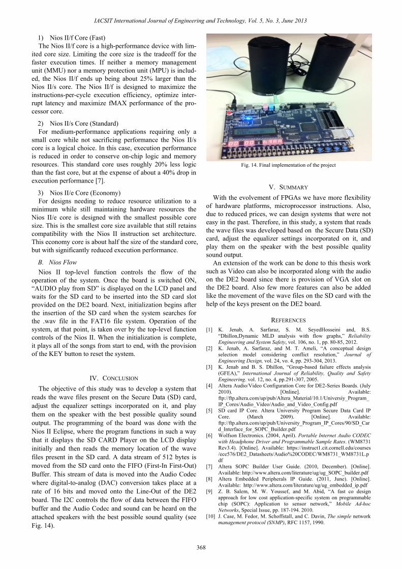
reads the wave files present on the Secure Data (SD) card, adjust the equalizer settings incorporated on it, and play them on the speaker with the best possible quality sound output. The programming of the board was done with the Nios II Eclipse, where the program functions in such a way that it displays the SD CARD Player on the LCD display initially and then reads the memory location of the wave files present in the SD card. A data stream of 512 bytes is moved from the SD card onto the FIFO (First-In First-Out) Buffer. This stream of data is moved into the Audio Codec where digital-to-analog (DAC) conversion takes place at a rate of 16 bits and moved onto the Line-Out of the DE2 board. The I2C controls the flow of data between the FIFO buffer and the Audio Codec and sound can be heard on the attached speakers with the best possible sound quality (see Fig. 14).
Fig. 14. Final implementation of the project
V. SUMMARY With the evolvement of FPGAs we have more flexibility
of hardware platforms, microprocessor instructions. Also, due to reduced prices, we can design systems that were not easy in the past. Therefore, in this study, a system that reads the wave files was developed based on the Secure Data (SD) card, adjust the equalizer settings incorporated on it, and play them on the speaker with the best possible quality sound output.
An extension of the work can be done to this thesis work such as Video can also be incorporated along with the audio on the DE2 board since there is provision of VGA slot on the DE2 board. Also few more features can also be added like the movement of the wave files on the SD card with the help of the keys present on the DE2 board.
REFERENCES [1] K. Jenab, A. Sarfaraz, S. M. SeyedHosseini and, B.S.
“Dhillon,Dynamic MLD analysis with flow graphs,” Reliability Engineering and System Safety, vol. 106, no. 1, pp. 80-85, 2012.
[2] K. Jenab, A. Sarfaraz, and M. T. Ameli, “A conceptual design selection model considering conflict resolution,” Journal of Engineering Design, vol. 24, vo. 4, pp. 293-304, 2013.
[3] K. Jenab and B. S. Dhillon, “Group-based failure effects analysis (GFEA),” International Journal of Reliability, Quality and Safety Engineering. vol. 12, no. 4, pp.291-307, 2005.
[4] Altera Audio/Video Configuration Core for DE2-Series Boards. (July 2010). [Online]. Available: ftp://ftp.altera.com/up/pub/Altera_Material/10.1/Universiy_Program_IP_Cores/Audio_Video/Audio_and_Video_Config.pdf
[5] SD card IP Core. Altera University Program Secure Data Card IP Core. (March 2009). [Online]. Available: ftp://ftp.altera.com/up/pub/University_Program_IP_Cores/90/SD_Card_Interface_for_SOPC_Builder.pdf
[6] Wolfson Electronics. (2004, April). Portable Internet Audio CODEC with Headphone Driver and Programmable Sample Rates. (WM8731 Rev3.4). [Online]. Available: https://instruct1.cit.cornell.edu/courses /ece576/DE2_Datasheets/Audio%20CODEC/WM8731_WM8731L.pdf
[7] Altera SOPC Builder User Guide. (2010, December). [Online]. Available: http://www.altera.com/literature/ug/ug_SOPC_builder.pdf
[8] Altera Embedded Peripherals IP Guide. (2011, June). [Online]. Available: http://www.altera.com/literature/ug/ug_embedded_ip.pdf
[9] Z. B. Salem, M. W. Youssef, and M. Abid, “A fast co design approach for low cost application-specific system on programmable chip (SOPC): Application to sensor network,” Mobile Ad-hoc Networks, Special Issue, pp. 187-194. 2010.
[10] J. Case, M. Fedor, M. Schoffstall, and C. Davin, The simple network management protocol (SNMP), RFC 1157, 1990.
IACSIT International Journal of Engineering and Technology, Vol. 5, No. 3, June 2013
368
[11] S. Moslehpour, K. Jenab, and B. S. Pabla, “Implementing a soft core NIOS II processor for VGA application,” International Journal of Engineering Research and Innovation, vol. 4, no. 2, pp. 12-26, 2012.
[12] K. Popovici, F. Rousseau, A. A. Jerraya, and M. Wolf, Embedded software design and programming of multiprocessor system-on-chip. New York: Springer, 2010.
[13] S. Moslehpour, K. Jenab, and S. Valiveti, “GPS time reception using altera SOPC builder and Nios II: Application in train positioning,” International Journal of Industrial Engineering and Production Research. vol. 23, no. 1, pp. 13-21, 2012.
[14] A. K. Swain, and K. K. Mahapatra, “Low cost system on chip design for audio processing,” in Proceedings of the International Multi-Conference of Engineers and Computer Scientists, vol. 2, Hong Kong, 2010.
[15] B. Fort, D. Capalija, Z. G. Vranesic, and S. D. Brown, “A multithreaded soft processor for SOPC area reduction,” in Proc. 14th Annual IEEE Symposium and IEEE Transactions on Field-Programmable Custom Computing Machines, FCCM '06. pp. 131-142, 2006.
[16] S. Sharma and A. Pal, “Implementation of web-server using altera DE2-70 FPGA development kit,” Bachelor’s Thesis. Department of Electronics and Communication Engineering. National Institute of Technology, Rourkela, India, 2010.
[17] X. Wang, “Multi-core system education through a hands-on project on FPGAs,” in Proc. of the Frontiers in Education Conference, FIE, 2011.
[18] J. Robinson, S. Vafaee, J. Scobbie, M. Ritche, and J. Rose, “The super soft small processor,” IEEE Transactions on Programmable Logic Conference (SPL), VI, pp. 3-8, 2010.
[19] M. Leeser, S. Hauck, and R. Tessier, “Field-programmable gate arrays in embedded systems,” EURASIP Journal on Embedded Systems. V2006, pp. 1-2, 2006.
[20] Z. Wang and P. Ning, “image capture and storage system based on SOPC,” in Proceedings of the 2010 3rd International Congress on Image and Signal Processing, CISP 2012, vol. 4, no. 1, pp. 1999-2002, 2010.
[21] J. O. Hamblen and T. S. Hall, “Using system on a programmable chip technology to design embedded systems,” IJCA, vol. 13, no. 3, pp. 1-11, 2006.
[22] My First NIOS II Software, Altera Corporation based on Altera Complete Design Suite Vrsion9.1. January 2010. [Online]. Available: http://www.altera.com/literature/tt/tt_my_first_nios_sw.pdf
[23] H-W. Liang, J-A. Li, and L-L. Kan, “Implementation of SD card music player using altera DE2-70,” in Proceedings of the 2011 International Conference on Multimedia and Signal Processing (CMSP), vol. 2, no. 1, 150-153, 2011.
[24] M. Zhang and H. T. Liu, “The design of the displaying system based on the SOPC embedded chips,” in Proc. International Conference on Electric Information and Control Engineering, ICEICE 2011, art. no. 5777471, pp. 5477-5480, 2011.
Saeid Moslehpour is an associate professor and department chair in the Electrical and Computer Engineering Department in the College of Engineering, Technology, and Architecture at the University of Hartford. He holds Ph.D. (1993) from Iowa State University and Bachelor of Science (1989) and Master of Science (1990) degrees from University of Central Missouri. His research interests include logic design, CPLDs, FPGAs,
Embedded electronic system testing and distance learning.
Kouroush Jenab is a senior member of IEEE, received the B.Sc. degree from the IE Department at Isfahan University of Technology (1989), the M.Sc. degree from the IE Department at Tehran Polytechnic (1992), and the Ph.D. degree from the Department of Mechanical Engineering at the University of Ottawa (2005). He served as a senior engineer/manager in auto, and high-tech industries for 18 years. He joined the National Research
Council Canada as a research officer where he participated in several international research projects. In 2006, he joined the Department of Mechanical and Industrial Engineering at Ryerson University, Toronto, as an assistant professor. Currently, Dr. Jenab is education chair of the Society of Reliability Engineering (SRE)-Ottawa Chapter. He has published over 81 papers in international scientific journals and conferences, edited a special issue on Applied Computational Techniques in Engineering and Technology for the International Journal of Industrial Engineering Computations, and produced over 29 technical reports.
Philip Weinsier is currently an associate professor and EEET program director at Bowling Green State University-Firelands. He received B.S. degrees in Physics and Industrial Education (1978), an M.S. degree in Industrial Education and Ed.D. degree in Vocational/Technical Education from Clemson University (1979 and 1990, respectively). Philip is a Fulbright Scholar, a lifetime member of the International Fulbright Association, and a member
of the European Association for Research on Learning and Instruction since 1989. Additionally, he has over 25 years of experience teaching applied engineering at the university.
Bharath Kumar Matcha received his bachelor of
technology degree in electronics and communication
engineering in May, 2008, from Vardhaman College
of Engineering affiliated with Jawaharlal
Technological University, India. He worked at
Infosys Technologies Limited as a Software Engineer
for a year. He got his degree in Electrical and
Computer Engineering from University of Hartford,
CT, with Embedded Systems as his major.
IACSIT International Journal of Engineering and Technology, Vol. 5, No. 3, June 2013
369