design of the line driver for adsl communication systems ... of the line driver for adsl...
TRANSCRIPT

Design of the Line Driver
for ADSL Communication Systems
by
Sergey Taryshkin
A thesis submitted to the Faculty of Graduate and Postdoctoral
Affairs in partial fulfillment of the requirements
for the degree of
Master of Applied Science
in
Electrical and Computer Engineering
Ottawa-Carleton Institute for Electrical and Computer Engineering
Carleton University
Ottawa, Ontario
©2011
Sergey Taryshkin

Library and Archives Canada
Published Heritage Branch
Bibliotheque et Archives Canada
Direction du Patrimoine de I'edition
395 Wellington Street Ottawa ON K1A0N4 Canada
395, rue Wellington Ottawa ON K1A 0N4 Canada
Your file Votre reference
ISBN: 978-0-494-87827-9
Our file Notre reference
ISBN: 978-0-494-87827-9
NOTICE:
The author has granted a nonexclusive license allowing Library and Archives Canada to reproduce, publish, archive, preserve, conserve, communicate to the public by telecommunication or on the Internet, loan, distrbute and sell theses worldwide, for commercial or noncommercial purposes, in microform, paper, electronic and/or any other formats.
AVIS:
L'auteur a accorde une licence non exclusive permettant a la Bibliotheque et Archives Canada de reproduire, publier, archiver, sauvegarder, conserver, transmettre au public par telecommunication ou par I'lnternet, preter, distribuer et vendre des theses partout dans le monde, a des fins commerciales ou autres, sur support microforme, papier, electronique et/ou autres formats.
The author retains copyright ownership and moral rights in this thesis. Neither the thesis nor substantial extracts from it may be printed or otherwise reproduced without the author's permission.
L'auteur conserve la propriete du droit d'auteur et des droits moraux qui protege cette these. Ni la these ni des extraits substantiels de celle-ci ne doivent etre imprimes ou autrement reproduits sans son autorisation.
In compliance with the Canadian Privacy Act some supporting forms may have been removed from this thesis.
While these forms may be included in the document page count, their removal does not represent any loss of content from the thesis.
Conformement a la loi canadienne sur la protection de la vie privee, quelques formulaires secondaires ont ete enleves de cette these.
Bien que ces formulaires aient inclus dans la pagination, il n'y aura aucun contenu manquant.
Canada

The information provided in this thesis is part of the research program
conducted by Professor T. Kwasniewski and his associates.
All research results provided in this thesis including tables, graphs and figures
but excluding the narrative part of the thesis can be used by Prof. T. Kwasniewski and
his associates for educational and research purposes including open publications. The
matter of intellectual property may be pursued collaboratively by Carleton University
and Prof. T. Kwasniewski as appropriate.
i i

Abstract
System solution for ADSL line driver is presented. The proposed solution
includes high-resolution 2mi-order AZ modulator as data encoder and high-efficiency
switching power amplifier. The modulator has two-state analog output signal that
allows easy integrating it with the amplifier.
The Verilog code of the A£ modulator is written, integrated in Cadence Virtuoso
Automated Design Environment and simulated. The signals delays within the modulator
are evaluated. They are found to be 10 times less compared to the clock signal period
provided that 0.18 |Lim CMOS is used for the modulator fabrication.
Full H-bridge architecture is selected for the switching power amplifier. The
dimensions of output switching NMOS/PMOS transistors in 0.18 ^m CMOS are
determined for the output signal power 20 dBm. The simulation showed that the power
efficiency of the amplifier is close to theoretical 50% level. The matching circuitry is
suggested to be implemented off-chip. This allows reducing on-chip power dissipation.
The proposed line driver is simulated thoroughly in Cadence Virtuoso ADE. It is
found that the dynamic range of the driver is 83 dB that corresponds to the data
resolution 13.5 bits. Missing Tone Power Ratio of the driver is more than 65 dB. The
frequency response of the line driver is flat within entire ADSL band. Demonstrated
performance of the proposed line driver meets all relevant ADSL specifications.

Table of Contents
Abstract iii
Table of Contents iv
List of Figures viii
List of Tables xii
Abbreviations xiii
1 Introduction 1
1.1 Motivation 1
1.2 Thesis Objective 3
1.3 Thesis Outline 4
2 ADSL Signal Specifications 5
2.1 ADSL Standards Overview 5
2.2 ADSL Signal Structure 8
2.3 Line Interface Considerations 13
3 Discussion of A£ Modulator for ADSL Line Driver 15
3.1 AZ Modulator Technique Overview 15
3.1.1 Sampling and Quantization 17
iv
3.1.2 Signal and Noise Transfer Functions of AE Modulators
3.2 Practical Implementations of AL Modulators
3.3 Selection of AS modulator Architecture for ADSL SLD
3.4 Conclusion
4 Switching Power Amplifier as a Potential ADSL Line Driver
4.1 The Discussion of Class D Power Amplifier
4.2 Efficiency of Switching Power Amplifiers with Matching Circuit
4.3 Efficiency of Switching Power Amplifiers with Low-pass Filter
4.4 Self-oscillating Power Amplifiers for ADSL Applications
4.5 Implementations of Switching Power Devices in Low-voltage CMOS
4.6 Switching Output Buffer with Wideband Transformer
4.7 Conclusions
5 ADSL Switching Line Driver with AE Modulator
5.1 AI Modulator Design
5.1.1 The Topology of AX Modulator
5.1.2 Verilog Modules
5.2 Switching Amplifier Design
5.3 System Verification
5.3.1 Test Benches and Tests Overview
39
5.3.2 The Test Bench and Verification of the AX Modulator 85
5.3.3 Line Driver Characterization 93
6 Conclusions and Future Work 101
6.1 Summary 101
6.2 Results Comparison 102
6.3 Thesis Contribution 107
6.4 Recommendations and Future Work 109
7 References Ill
Appendix A - Matlab Processing Toolbox 117
A. 1 SDM Main Processor 117
A2 calcSNR 121
A.3 sinusx 123
A.4 hannSTD 123
A.5 histo 123
A.6 dbp 124
Appendix B AE Modulator Source Code 125
B.l Integrator 125
B.2 Adder 1 127
B.3 Adder 2 128
vi

B.4 Relay 129
Appendix C VerilogA Source Code 131
C. 1 16-bit Analog-to-Digital Converter 131
C.2 16-bit Digital-to-Analog Converter 134
vi i

List of Figures
Figure 2.1 ADSL Spectrum Allocation, Not-overlapped Spectrum Operations 7
Figure 2.2 Data Allocation in Noisy Lines 9
Figure 2.3 Frequency Representation of OFDM Signal 10
Figure 2.4 ADSL Transmitter, OFDM Modulator 11
Figure 3.1 lsl Order Sigma-Delta Modulator 16
Figure 3.2 Signal Sampling 17
Figure 3.3 Probability Distribution of Quantization Error 18
Figure 3.4 Power Spectrum Density of Quantization Error 18
Figure 3.5 Power Spectral Densities of Quantization Errors 20
Figure 3.6 Oversampling Example, L=2 21
Figure 3.7 N-Order AI Modulator Functional Block Diagram 22
Figure 3.8 Signal and Noise Transfer Functions of Low-Pass A£ Modulators 23
Figure 3.9 Band-pass AZ Modulator of 2nd Order 24
Figure 3.10 Switched Capacitor Integrator 25
Figure 3.11 Switched Current Integrator 26
Figure 3.12 Missing Tone Power Ratio [24J 29
Figure 3.13 Simulink Model of 2ml-order AZ Modulator 30
Figure 3.14 Internal Signals of 2nd Order AI modulator 33
vi i i

Figure 3.15 Signal Spectrum of 2nd-order AS Modulator's Simulink Model,
fiN = 250 kHz 34
Figure 3.16 Signal Spectrum of 2nd-order AS Modulator's Simulink Model,
fiN = 250 kHz 35
Figure 3.17 MTPR Test Toolbox 36
Figure 3.18 Bits Loading Distribution 38
Figure 3.19 Signal Spectra at the Input and Output of 2nd-Order AS Modulator ...38
Figure 4.1 Class D Power Amplifier 42
Figure 4.2 Power Transfer Efficiency 44
Figure 4.3 Equivalent Electric Diagram of Switching Amplifier 45
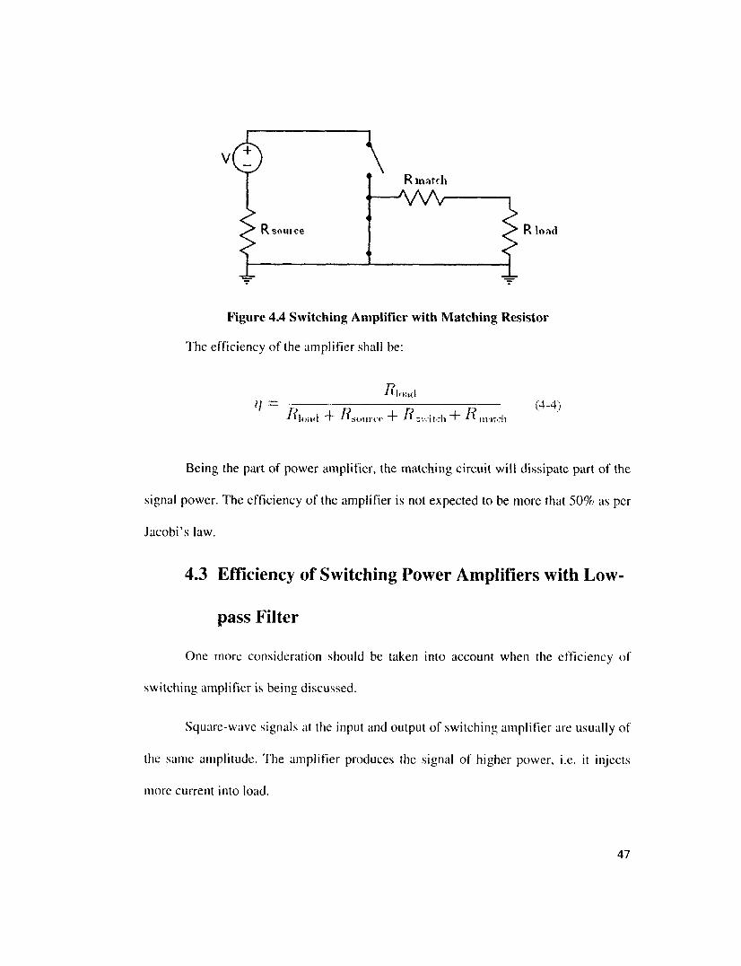
Figure 4.4 Switching Amplifier with Matching Resistor 47
Figure 4.5 Switching Amplifier with Low-pass Filter 48
Figure 4.6 Basic Zero-order SOPA 50
Figure 4.7 First-order SOPA 50
Figure 4.8 Dual SOPA Topology 51
Figure 4.9 Block Schematic of High-voltage Driver 53
Figure 4.10 Output CMOS Buffer with Impedance Transformer and LPF 56
Figure 4.11 Full H-bridge Switching Buffer 57
Figure 5.1 2nd Order Sigma-Delta Modulator 63
ix

Figure 5.2 Functional Block Diagram of Ideal Integrator 65
Figure 5.3 Saturation Schematics 67
Figure 5.4 Signal Code Space 70
Figure 5.5 AS Modulator Schematic 71
Figure 5.6 Functional Block Diagram of Switching Amplifier with Connected Load
74
Figure 5.7 Half H-bridge Switching Amplifier Schematic 75
Figure 5.8 Half H-bridge Amplifier Pulses Shape 78
Figure 5.9 Full H-bridge Switching Amplifier 80
Figure 5.10 Full H-bridge Switching Amplifier Pulses Shape 83
Figure 5.11 Sigma-Delta Modulator Test Bench 86
Figure 5.12 AS Modulator's Internal Signals 87
Figure 5.13 Signals Histograms of the AS Modulator 88
Figure 5.14 Signal Spectrum of 2nd-order AS Modulator, fiN = 250 kHz,
BW = 500 kHz 89
Figure 5.15 Signal Spectrum of 2nd-order AS Modulator, f|N = 250 kHz,
BW = 500 kHz 90
Figure 5.16 DMT Signal Instantiation at the AS Modulator's Input 91
Figure 5.17 ADSL Signal Processor for MTPR Evaluation 92
x
Figure 5.18 MTPR of 2nd-order AZ Modulator 92
Figure 5.19 ADSL Line Driver Schematic 94
Figure 5.20 Signal Spectrum of the Line Driver with Switching Power Amplifier,
f,N = 250 kHz, BW = 500 kHz 95
Figure 5.21 Signal Spectrum of the Line Driver with Switching Power Amplifier,
fiN = 250 kHz, BW = 500 kHz 96
Figure 5.22 Dynamic Range of the Line Driver, f^ = 250 kHz, BW = 500 kHz....97
Figure 5.23 Dynamic Range of the Line Driver, fiN = 250 kHz, BW = 500 kHz....98
Figure 5.24 Frequency Range of the Line Driver, BW = 1 MHz 98
Figure 5.25 MTPR of the ADSL Line Driver 100
Figure B. 1 Integrator Symbol 126
Figure B.2 Adder I Symbol 128
Figure A.3 Adder 2 Symbol 129
Figure B.4 Relay Symbol 130
Figure C.l 16-bit ADC Symbol 134
Figure C.2 16-bit DAC Symbol 135
xi

List of Tables
Table 1 AL Modulator's Modules Delay 69
Table 2 Half H-bridge Switching Amplifier 77
Table 3 Half H-bridge Switching Amplifier 79
Table 4 Full H-bridge Switching Amplifier 81
Table 5 Full H-bridge Switching Amplifier 82
Table 6 AX Modulators 104
Table 7 Switching Power Amplifiers 106
xi i

Abbreviations
ADE - Automated Design Environment
ADSL - Asymmetric Digital Subscriber Line
BW - Band Width
CF - Crest Factor
CO - Central Office
CPE - Customer Premises Equipment
CSV - Comma Separated Values
DFT - Digital Fourier Transform
DMT - Discrete Multi-Tone
DR - Dynamic Range
DSL - Digital Subscriber Line
EDA - Electronic Design Automation
FFT - Fast Fourier Transform
IFFT - Inverse Fast Fourier Transform
ITU - International Telecommunication Union
MASH - Multi-stage Noise Shaping
OFDM - Orthogonal Frequency Division Multiplexing
xi i i

OSR - Over - Sampling ratio
PA - Power Amplifier
PAPR - Peak to-Average Power Ratio
POTS - Plain Old telephone Service
PSD - Power Spectrum Density
QAM - Quadrature Amplitude Modulation
SC - Switched Capacitors
SFDR - Spurious Free Dynamic Range
SI - Switched Currents
SLD - Switching Line Driver
SNR - Signal-to-Noise ratio
SNDR - Signal-Noise Distortion Ratio
SOPA - Self-Oscillating Power Amplifier
RTL- Register Transfer Level
VDSL - Very High Speed Digital Subscriber line
UWB - Ultra Wide Band
xiv

1 Introduction
1.1 Motivation
Modern DSL communication systems require signal processors dealing with
high data rates combined with data conversion resolution of 12 - 14 bits. This
requirement goes along with the progress in silicon fabrication processes. Advanced
functionalities built in the digital part of the communication system can be easily
implemented with modern CMOS technologies that allow fabricating less expensive
devices of smaller size.
At the same time, small physical dimensions of the transistor built with modern
silicon technologies make the design of analog part of the devices difficult. In
particular, the design of line drivers for copper cable gets challenging. The line drivers
create a power bottleneck due to high Peak-to-Average Power Ratio (PAPR) of DSL
signal [ 11.
Class A/B power amplifiers are still often used in DSL products. However, their
efficiency and performance drop down significantly with low supply voltage headroom
of modern CMOS devices. Class A/B line drivers might be replaced with Class G, Class
H, Class K and other high-efficient power amplifiers 11, 2). Even though, it is very
difficult to implement these solutions in low-voltage silicon processes due to high
PAPR and high linearity requirements of the quadrature amplitude modulation of
Discrete Multitone (DMT) signal used in most DSL systems.
1

Class D Power Amplifiers (PA) are considered as very promising solution in
low-voltage devices. Switching Line Drivers (SLD) based on Class D PAs are well
known for their high efficiency, for example, in audio applications.
The Self-Oscillating Power Amplifier (SOPA) proposed by T. Piessens and M.
Steyaert [3] can also be classified as a switching line driver. The authors claimed
relatively high power efficiency of the line driver when it used for ADSL and VDSL
applications.
The SLD can be built with Delta-Sigma (AX) modulator as a driving circuit [ 11.
One-bit data stream from the AX modulator is suitable to feed baseband switching
power amplifier. AX modulators of a proper order provide quite reasonable signal
dynamic range. The combination of the modulator and switching amplifier can be a
power-effective solution for DSL line drivers.
AX modulators are widely used in DSL products. In particular, the modulators
allow cost-effective solutions for A/D converters in the receiver path of DSL Analog
Front End. However, the number of publications on AX modulators in SLD is very
limited. This solution seems challenging. AX modulators in the Rx path of DSL systems
often have multi-bit internal feedback and output to get required accuracy and dynamic
range. When used as a driver for the switching power amplifier, multi-bit AX
modulators are not convenient. The necessity to have single-bit output signal forces a
designer to increase the sampling frequency to maintain required accuracy/resolution of
the modulator, but the frequency headroom is always limited due to technology
restrictions. The trade-off between the accuracy and the sampling frequency is
2

application specific and is determined based on relevant requirements.
The switching power amplifiers are attractive as line drivers due to their high
power efficiency. The other advantage of using the switching PAs is the opportunity to
employ mixed CMOS technology that doesn't require fine schematic tuning.
It should be noted that the AZ modulators of order two and higher are usually
implemented as analog circuits. It is beneficial to design the modulator as pure digital
device and then to build it using standard CMOS process. Together with the switching
PA, this would allow getting cost-effective solution of DSL line driver.
1.2 Thesis Objective
This work represents the study of AZ modulator and switching power amplifier
when they are used as the DSL line driver. Accordingly, the thesis objectives can be
defined as follows:
• Analysis and justification of AZ modulator's topology suitable for DSL
applications;
• Design of the AZ modulator and its verification in Cadence Virtuoso ADE;
• Design of switching power amplifier of 20 dBni peak power and its
verification in Cadence Virtuoso ADE;
• Characterization of the line driver composed of the AZ modulator and the
switching power amplifier against the relevant DSL specifications.
1.3 Thesis Outline
The thesis is organized in accordance with the objectives defined above.
Section 2 provides the overview of DSL specifications that are relevant to the
subject of the thesis. The signal structure and the modulation schemes used in the DSL
systems are discussed. Details of the electrical interface specific to the DSL lines are
studied.
Section 3 is devoted to the design of the AL modulators. The section begins with
the discussion of the modulator's topologies and their performance. The overview of the
modulator's implementations is given accompanied by the relevant technical
publications. The architecture of the AZ modulator proposed in this thesis work is
justified.
The design of the switching power amplifier is discussed in Section 4. The
signal features and the details of the line interface that might affect the efficiency of the
switching PAs are studied.
The detailed design of the switching line driver proposed in this work is
provided and then characterized in Section 5. The performance of the line driver is
evaluated based on the simulations in Cadence Virtuoso ADE. The simulation results
are processed using Matlab and Simulink.
The final section provides the summary of the work.
The Matlab scripts used in this work and Verilog code of the AS modulator are
given in the Appendixes.
4

2 ADSL Signal Specifications
DSL technology takes advantages of comprehensive digital signal processing
(DSP) algorithms and data coding schemes. DSL communication systems have built-in
intelligence to accommodate the wide varieties of data transmission signal conditions
encountered with each connection through the telephone switching network.
Sophisticated ASIC devices have been developed for DSL lines to implement real-time
processing algorithms for these communication links [4. 5, 6|.
At the same time, as in case with almost any system, DSL ones still require
analog electronics to put the signal into the phone line and to pick up small signals
received at the other end. These analog subsystems should be designed properly to
address specific requirements of DSL communication links.
There are several DSL technologies in a market, such as HDSL, VDSL, ADSL,
to name the most generic ones. The major difference between the technologies, as they
affect the line driver, is the signal structure and the amount of power put in the line by
the line driver. The further discussion and study will be focusing on ADSL standard.
2.1 ADSL Standards Overview
Main ADSL specifications are contained in two documents published by
International Telecommunication Union (ITU). The first document is G.992.1 |7| for
the systems being referred to as full-rate ADSL or G.DMT, and the second one is
5

G.992.2 18], a lower data rate solution often called G.Lite. Both systems use the DMT
technique to encode transmitted data.
In full-rate ADSL systems a frequency band BW =1.1 MHz is split for up to
256 separate tones (also called sub-carriers or sub-channels) each spaced 4.3125 KHz
apart. With each tone carrying separate data, the technique operates as if 256 separate
modems were running in parallel. To further increase the data transmission rate, each
individual tone is quadrature-amplitude modulated (QAM). The data to be transmitted is
used to create a unique amplitude- and phase-shift combination for each carrier tone by
using I and Q components of the signal. This combination defines so-called data
symbol, which is updated at 4.3125 KHz rate. Full rate ADSL uses up to 15 bits of data
to create each symbol. This results in a theoretical maximum of 60Kb/s for each tone. If
all 256 tones are used in parallel, the total data rate can be as high as 15.36 Mb/s.
In G.Lite ADSL system the frequency band is limited to BW = 0.55 MHz,
accordingly, the maximum number of sub-carriers is reduced to 128, and eight bits per
sub-carrier are used only. This brings the theoretical maximum data rate down to 4.096
Mb/s.
In ADSL applications, the tones are allocated depending on the direction of
communication, as shown in Figure 2.1. Most of the tones are used for data transfer
from the Central Office (CO) to an end-user modem often referred to as Customer
Premises Equipment (CPE). This direction of communication is called "downstream".
The direction of communication from the CPE to the CO is called "upstream". The
assignment of more tones for the downstream direction makes sense from an Internet-
6

access point of view as most users download more information than they upload. Most
upstream communication with a server is simply to request information to be sent
quickly downstream. This difference in data rates up- and downstream is the reason that
ADSL is called asymmetric DSL.
Maximum Power Spectral Density (PSD) of all tones is specified in G.922.1 and
G.992.2 standards as shown in Figure 2.1 below. The PSD specifications determine the
amount of signal power that has to be put on the phone line. The power levels are
restricted to minimize crosstalk and interference into other phone lines contained in
wire bundle en route to and from the central office.
N 5 E 00 TS £ </> £ CD a
B a> a (A a> s o a
-34.5 dBmJHz
36.5 dBm/Hz
UPSTREAM J DOWNSTREAM
25.875 138
U-BOTH-
552
-O.LITE
- G.DMT-
1104 Frequency, kHz
Figure 2.1 ADSL Spectrum Allocation, Not-overlapped Spectrum Operations
The downstream signal power is much higher than the upstream one because of
wider bandwidth used for the transmission. For the same reason, full-rate G.DMT
ADSL carries more line power than G.Lite for downstream transmissions. Upstream
power is the same for both full-rate and G.Lite DSL implementations.

ADSL line driver should be able to generate the signal with power 13 dBm for
upstream and up to 20 dBm for downstream channels.
2.2 ADSL Signal Structure
As mentioned above, DMT technique splits the frequency bandwidth into a set
of smaller sub-channels. The data is encoded in each sub-channel using Quadrature-
Amplitude Modulation (QAM). The QAM order in each sub-channel is defined by
Signal-Noise Ratio (SNR) that is measured dynamically for each tone.
The intelligence is built in DSL modems mostly to obtain the fastest data rate for
any set of line conditions. In order to gauge the conditions on a line CO modem initiates
so-called "training-up" session. During this session, the modems at both ends of a line
transmit maximum and equal amount of data per tone/sub-channel. When "training-up"
signal sequence is received at the opposite side of the line, the modems processors
calculate errors and determine the signal-noise ratio in each sub-channel. The SNR
distribution throughout the tones is then sent back to an originating modem. The
modem's DSP automatically allocates less data in "noisy" sub-channels using QAM of
lower order. Accordingly, QAM of higher order is used in "clean" sub-channels that
allow pumping more data in them. This algorithm maximizes the data throughput for a
particular line. Figure 2.2 illustrates the algorithm of data allocation used in DSL
systems.
Noise can contaminate any number of sub-channels to render them completely
unusable, or useful, but with less than maximum possible data capability. Additionally,
8
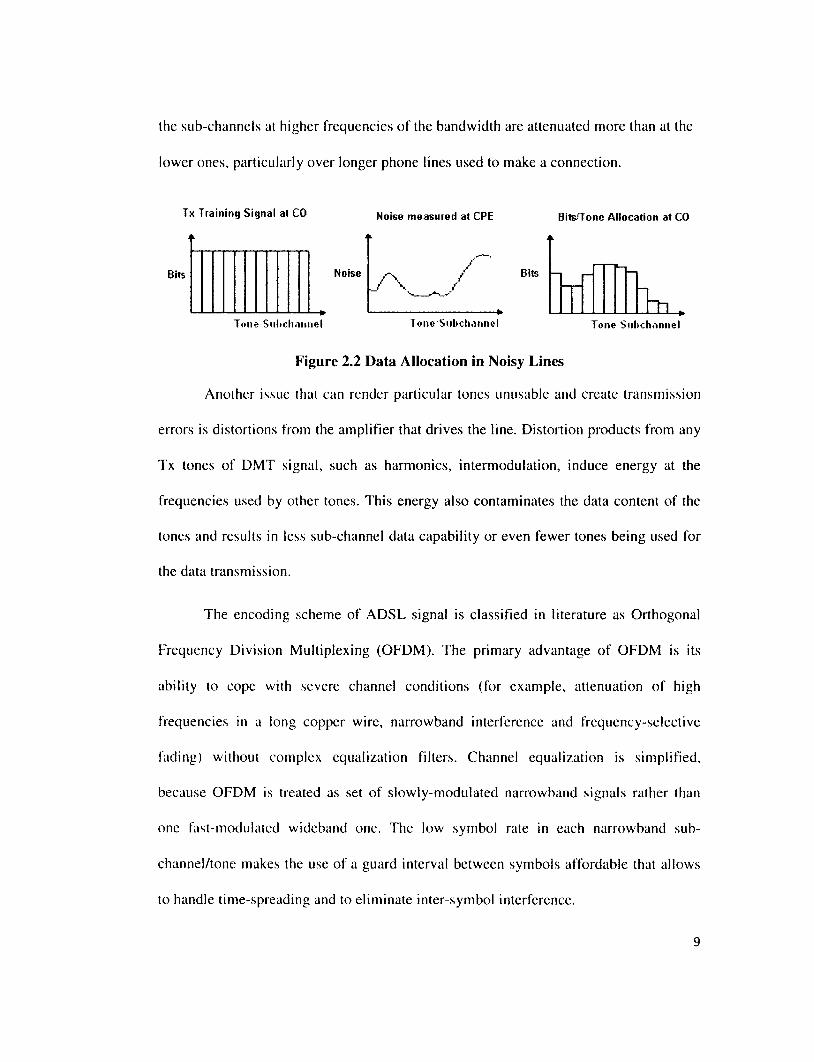
the sub-channels at higher frequencies of the bandwidth are attenuated more than at the
lower ones, particularly over longer phone lines used to make a connection.
Tx Training Signal at CO Noise measured at CPE Bits/Tone Allocation at CO
Bits
Tone Subchannel Tone.'Subchannel Tone Subchannel
Figure 2.2 Data Allocation in Noisy Lines
Another issue that can render particular tones unusable and create transmission
errors is distortions from the amplifier that drives the line. Distortion products from any
Tx tones of DMT signal, such as harmonics, intermodulation, induce energy at the
frequencies used by other tones. This energy also contaminates the data content of the
tones and results in less sub-channel data capability or even fewer tones being used for
the data transmission.
The encoding scheme of ADSL signal is classified in literature as Orthogonal
Frequency Division Multiplexing (OFDM). The primary advantage of OFDM is its
ability to cope with severe channel conditions (for example, attenuation of high
frequencies in a long copper wire, narrowband interference and frequency-selective
fading) without complex equalization filters. Channel equalization is simplified,
because OFDM is treated as set of slowly-modulated narrowband signals rather than
one fast-modulated wideband one. The low symbol rate in each narrowband sub
channel/tone makes the use of a guard interval between symbols affordable that allows
to handle time-spreading and to eliminate inter-symbol interference.
9
Noise Bits
_Lh_

In OFDM, the sub-channel frequencies are selected so that the narrowband
signals are orthogonal to each other, meaning that cross-talk between the sub-channels
is eliminated and inter-carrier guard bands are not required.
The orthogonality requires that the space Af between sub-channel frequencies is
reverse proportional to the duration of data symbol T:
Af = 1/T
Orthogonality increases the spectral efficiency of OFDM signals by allowing the
overlapping of spectra of the sub-channel signals. The representation of 4-tone OFDM
signal in frequency domain is shown in Figure 2.3 below [91.
Figure 2.3 Frequency Representation of OFDM Signal
The harmonics of narrowband signals/tones around their sub-channel central
frequencies overlap and partially compensate each other as their phase switches by 180°
from one harmonic to the next one. As a result, the noise floor due to interference
between sub-channels is relatively low and grows slower with the number of sub
channels compared to non-orthogonal signals.
10

The orthogonality allows an easy implementation of OFDM receiver and
transmitter using FFT and IFFT algorithms respectively. Simplified block diagram of
Tx modulator is shown in Figure 2.4 below.
Constellation Mapping
XN
DAC Parallel
Serial Inverse
FFT
Figure 2.4 ADSL Transmitter, OFDM Modulator
Sn is a serial stream of binary digits. This data stream is first de-multiplexed into
N parallel streams, and each one mapped to a symbol stream Xj using modulation
constellation (QAM for ADSL). The constellations could be of different order, so some
streams may carry a higher bit-rate than others.
An inverse FFT is computed on each set of symbols, producing a set of complex
time-domain samples. The real and imaginary components are first converted to the
analogue domain using Digital-to-Analog Converters (DAC's). The analog signals can
be then up-converted to higher frequency and quadrature-mixed for further
amplification in the transmitter.
11

No signal up-conversion is required in DSL devices, and baseband signal from
DAC output is applied to line terminals directly or through power amplifier, if
necessary.
Baseband DMT signal placed on the line looks basically like white noise
because many signals of changing amplitude and phase are combined simultaneously.
The changes of each signal are considered random as they result from an arbitrary
sequence of data bits comprising the transmitted information. The signals can stack
from time to time and create a large peak signal. If this peak is not processed properly
(for example, if the line-driver amplifier clips), data error can occur.
Term Peak-to-Average Power-Ratio (PAPR) is used in literature to characterize
such signal behavior. This term is similar to the term of Crest Factor (CF). The PAPR
determines the peak value of the voltage put on the line over a time with respect to the
RMS voltage level:
Vpeak = PAPR * Vrms (2-1)
For OFDM signals, PAPR depends on the number of tones/sub-carriers
comprising the signal. For ADSL signal with 256 tones PAPR can be as high as 12 dB.
In reality, the number of tones used during some particular communication session is
less than maximum possible. Also data capability of each sub-carrier/tone is different.
This usually reduces PAPR value a bit.
However, the PAPR remains high enough to challenge the design of ADSL line
driver. This factor determines both the minimum supply voltage required to prevent
clipping of the signal at the output of analog line driver and also the peak output power
12

capability of the driver. The PAPR actually defines the dynamic range of the line driver
and, hence, its efficiency, in particular, when power amplifiers of Class A and B are
used.
2.3 Line Interface Considerations
The characteristic impedance of ADSL communication line is 100 f2. This
determines the current at the line input terminals if the supply voltage of the line driver
is defined.
A transformer is usually used to connect the DSL transceiver to the line. The
transformer is selected for a flat, distortion-free frequency response from 20 kHz to 1-2
MHz to cover the full operational frequency band.
One of the functions of the transformer is to provide DC isolation between DSL
modem front-end and the line. At the same time, the turn's ratio of the transformer can
be used to provide a voltage gain to the signal routed to the line. The turn's ratio is
defined mostly by the power supply voltage for the line-driver amplifiers. By stepping
up the signal from the driver to the line via the transformer, the signal voltage swing at
the amplifiers output can be reduced. As an ideal transformer has unity power gain, i.e.
equal power in the primary and secondary coils, while the voltage is stepped up, the
current is stepped down. The consequence of using a step-up transformer is beneficial in
that lower, more convenient supply voltage can be used, but the amplifiers must have
higher current driver capability.
The negative impact of step-up transformer is that it steps down the signal
coming back from the phone line, so the sensitivity of DSL modem might saturate.
13

Appropriate modem's front-end architectures should be employed to avoid or to
minimize the sensitivity degradation of the modem with transformer line interface.
14

3 Discussion of A£ Modulator for ADSL Line
Driver
As shown in Figure 2.4 above the signal generated by the OFDM modulator is
routed to the DAC to produce its analog representation. The DAC might be followed by
an amplifier that is necessary to increase the power of the analog signal to the required
level.
The manipulations with OFDM signal in analog domain are challenging.
Although the design solutions of 15-16 bit DACs are known, their application for
ADSL systems might be impractical due to unique set of resolution, speed and dynamic
range parameters. Also, the design of linear power amplifier for the signals with high
PAPR is difficult. As noted earlier, the linear amplifier appears to be a bottleneck of
ADSL modem.
As an alternative design solution of ADSL transmitter path, Switching Line
Driver composed of AI modulator followed by the switching power amplifier can be
used. The AL modulator converts the signal from the IFFT DSP to single-bit data
stream, which is then appropriately amplified to maintain required signal swing at the
input terminals of the line.
3.1 AL Modulator Technique Overview
AZ modulator presents attractive solution. It samples signals at much higher rate
than the Nyquist rate. The over-sampling relaxes anti-alias requirements and actually
15
trades the resolution in time for resolution in signal amplitude. Noise shaping property
of the AS modulator allows it to achieve high resolution even when simple components
such as single-bit quantizer are used.
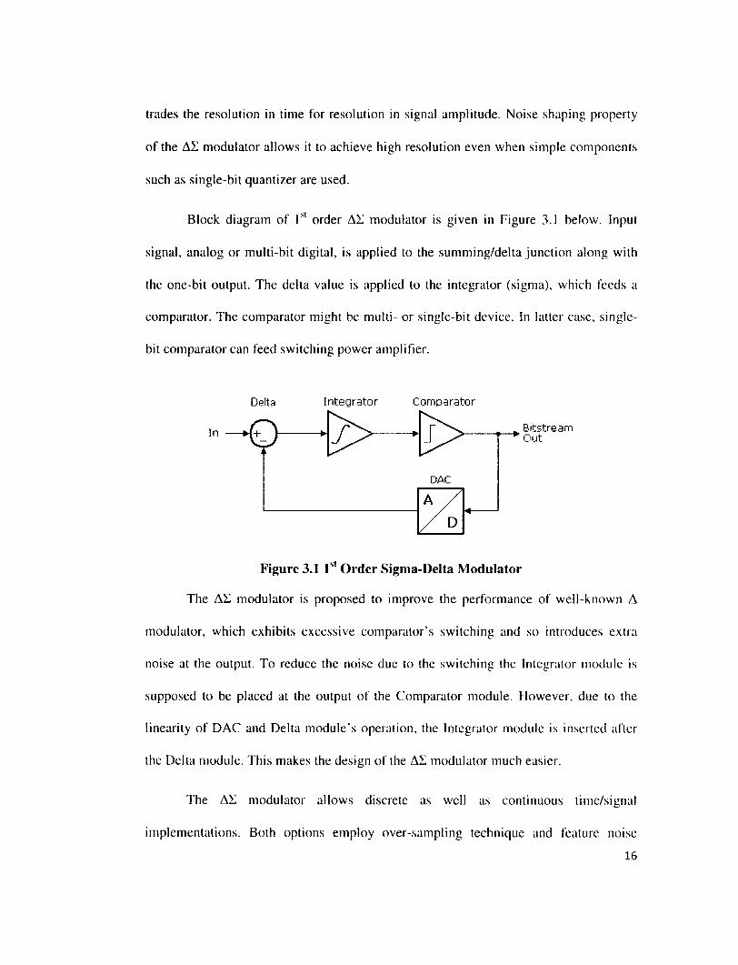
Block diagram of 1st order AS modulator is given in Figure 3.1 below. Input
signal, analog or multi-bit digital, is applied to the summing/delta junction along with
the one-bit output. The delta value is applied to the integrator (sigma), which feeds a
comparator. The comparator might be multi- or single-bit device. In latter case, single-
bit comparator can feed switching power amplifier.
Delta Integrator Comparator
Bitstrearn Out
Figure 3.1 1st Order Sigma-Delta Modulator
The AS modulator is proposed to improve the performance of well-known A
modulator, which exhibits excessive comparator's switching and so introduces extra
noise at the output. To reduce the noise due to the switching the Integrator module is
supposed to be placed at the output of the Comparator module. However, due to the
linearity of DAC and Delta module's operation, the Integrator module is inserted after
the Delta module. This makes the design of the AS modulator much easier.
The AS modulator allows discrete as well as continuous time/signal
implementations. Both options employ over-sampling technique and feature noise
16

shaping to achieve high signal resolution. Discrete AI modulator is studied further for
the sake of the application being considered.
A quick review of quantization noise theory and signal sampling theory is useful
before diving deeper into the AE modulator details.
3.1.1 Sampling and Quantization
In discrete applications signals are represented by sequence of the signals
samples taken at equidistant time intervals Ts. Each sample is approximated by a digital
code of finite length, or quantized.
Shannon's sampling theorem states that the sampling frequency fs=l/T.s should
be at least twice higher that the signal bandwidth F^w in order to recover the sampled
signal back to continuous-time without distortion. Sampling frequency fs=2-Fnw is
called Nyquist frequency. Also, when signal is sampled, its spectrum is copied and
mirrored at multiples of the sampling frequency as shown in Figure 3.2 below.
Continuous Signal X(t) Oescrete Signal Xn
Ampiltude Power Spectrum Density Amplitude Power Spectrum Density
Frequency 1
fs fs 3fs 2fs Frequency T T
Figure 3.2 Signal Sampling
Mirrored signal spectrum components are called aliases. Since aliasing is
produced above and below signal original spectrum, the signal must be low-pass filtered
before being sampled. Otherwise, its high-frequency content will produce aliases in the
17

baseband. Also, since high-frequency aliases are usually unwanted, they must be
filtered out during signal conversion to continuous-time signal representation. Both pre-
sampling and post-sampling filtering is referred to as anti-alias filtering.
The signal sampled at some moment of time is represented by some number that
corresponds to its amplitude at that time. With a B-bit code length, there are 2B different
available numbers that can be used to characterize the signal amplitude. The amplitude
is rounded off to the closest number. This is called signal quantization. The quantization
error e|n|, i.e. the difference between the actual signal amplitude and its round-off
value, is considered as a white noise with zero mean value and uniform probability
distribution function P(e) as shown in Figure 3.3 below.
P(e) A
-Q/2
P -1
( )
Q/2
Figure 3.3 Probability Distribution of Quantization Error
In the drawing above Q is a quantization step.
Since the quantization error is random, i.e. white noise, the power spectrum
density of the error Se is also uniform within Nyquist frequency band.
S„(f] S =
-> f -fs/2 U 2
Figure 3.4 Power Spectrum Density of Quantization Error
18

The variance or the power of the quantization error is calculated as follow.
Signal-to-quantization-noise ratio (SQNR) is one of the most important
parameters when evaluating digital systems. For sinusoidal signal of maximum-level
amplitude A =2HIQ the SQNR can be easily calculated and is as follow.
When signal sampling frequency is higher than Nyquist frequency fso = L*fs,
the quantization error e'[n], i.e. the difference between the actual signal amplitude and
its round-off value, is the same as with sampling frequency fs. It is safe to assume that
there is no change in the variance, i.e. in the power, of the quantization errors e[n] and
e'lnj:
It is also evident that since the sampling interval is TSo = l/fso» the power of the
quantization error is spread in [-fso/2, +fso/2] frequency band, which is larger that
| -fs/2. +f.s/2 ] Nyquist band. Since the power of the error is the same, the power spectral
density is smaller by a factor L.
( P \ SNOR-10 • log - -*• =10 -log
^ U; £1 12
*6.025 + 1.76 [dBJ (3-2)
(3-3)
19

s , ( i i S
' ' f.
<J2
Figure 3.5 Power Spectral Densities of Quantization Errors
As in the case of over-sampling, the signal bandwidth |-fs/2, +fs/2] is not
changed, the power of quantization error in the frequency band of interest is smaller by
a factor L.
SNOR = 10-los P
P i'L 6.02 • 5 +1.76 +10• log{ L ) . [dB]. (3-4)
/ L
The over-sampling has another immediate advantage: it relaxes the anti-aliasing
filter requirements by allowing a gentle roll-off of the filter. Due to high sampling
frequency, the replicas of the signal spectrum at multiples of the sampling frequency are
spaced far away from each other, so a large stop-band is allowed for the anti-aliasing
filter. Low-order simple LPF's can be used.
20

J-U, ¥ 1 ¥ r-1 / 2 f,, 3f.,/2 2f,,
->t
I X \ \ -r r
f. 2 f.. 3iJ2 21
Figure 3.6 Over-sampling Example, L=2
3.1.2 Signal and Noise Transfer Functions of AE Modulators
One of the inherent features of AE modulators is noise shaping. In combination
with the over-sampling, noise shaping allows to further reduce the quantization noise
within the band of interest. Noise shaping, as the name implies, involves attenuating the
in-band quantization noise at the expense of amplifying noise in the out-of-band region.
The resulting spectrum at the output has minimum in-band quantization noise and large
out-of-band noise. If a low-pass filter is applied to the output, the out-of-band noise can
be eliminated at all, if necessary.
For the sake of analysis the quantization noise is often modeled as a random
noise from the generator applied to the output of the modulator as shown in Figure 3.7
below.
21
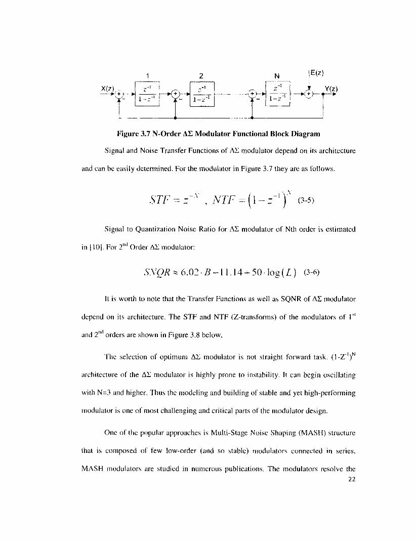
Y(z)
V-1 -z
Figure 3.7 N-Order AT, Modulator Functional Block Diagram
Signal and Noise Transfer Functions of AE modulator depend on its architecture
and can be easily determined. For the modulator in Figure 3.7 they are as follows.
STF = ;"*v . NTF = (1 - r 1)' tw>
Signal to Quantization Noise Ratio for AE modulator of Nth order is estimated
in 1101. For 2 ,Hl Order AX modulator:
SXOR * 6.02 -5-11.14 + 50 • log (L ) (3-6)
It is worth to note that the Transfer Functions as well as SQNR of AS modulator
depend on its architecture. The STF and NTF (Z-transforms) of the modulators of 1M
and 2ml orders are shown in Figure 3.8 below.
The selection of optimum AE modulator is not straight forward task. (1-Z"')N
architecture of the AE modulator is highly prone to instability. It can begin oscillating
with N=3 and higher. Thus the modeling and building of stable and yet high-performing
modulator is one of most challenging and critical parts of the modulator design.
One of the popular approaches is Multi-Stage Noise Shaping (MASH) structure
that is composed of few low-order (and so stable) modulators connected in series.
MASH modulators are studied in numerous publications. The modulators resolve the
22

stability problem of high-order structures in the expense of more complicated
architecture.
i •
i; • • : •'
i 1st Order
NTF
STF
. ...f.
• , ;
c - i :
i '
Freauency (rad'sec
NTF i 1
STF
2nd Order . . . ' ]
!
. . . . . . . . . . . . . . . . I • i > 1 ! 1 l i , . . . ! : •
. ; , . f.
Figure 3.8 Signal and Noise Transfer Functions of Low-Pass AE Modulators
The AS modulator in Figure 3.7 above is classified as low-pass modulator. Low-
pass modulator can be modified to band-pass by replacing the integrator z '*(l-z for
the resonator with transfer function z"2*( 1 -z 2)"'.
23

2 E(z)
X( 7 ) 2
>l" -f v • • A" 1-
+ . — 1 Figure 3.9 Band-pass A£ Modulator of 2nd Order
Band-pass AS modulators maintain the advantages of their low-pass
counterparts, i.e. reduced quantization error due to over-sampling and noise shaping.
The central frequency and bandwidth of the modulators depends on over-sampling
frequency value, the order and architecture of the modulator.
The publications related to band-pass AI modulators discuss mostly the devices
with signal central frequency 2-10 MHz and bandwidth up to 200 kHz 112, 13, 14],
These modulators are very convenient for digitizing narrowband IF signals. At the same
time, they are not suitable for DSL applications, which spectra are located close to the
base band, and the bandwidth can cover few MHz range.
Further study will consider low-pass AS modulators only.
Switched-capacitor (SC) technique is dominated approach in the design of
discrete-time AX modulators. The technique uses linear on-chip capacitors to store a
signal (or charge). By controlling switches and employing operational amplifiers, the
charges can be manipulated and shifted from one capacitor to the other.
3.2 Practical Implementations of AZ Modulators
24
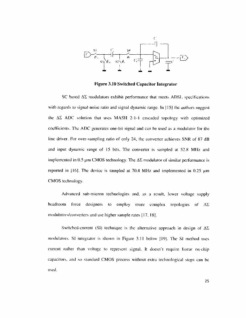
c
Figure 3.10 Switched Capacitor Integrator
SC based AL modulators exhibit performance that meets ADSL specifications
with regards to signal-noise ratio and signal dynamic range. In [ 151 the authors suggest
the AL ADC solution that uses MASH 2-1-1 cascaded topology with optimized
coefficients. The ADC generates one-bit signal and can be used as a modulator for the
line driver. For over-sampling ratio of only 24, the converter achieves SNR of 87 dB
and input dynamic range of 15 bits. The converter is sampled at 52.8 MHz and
implemented in 0.5 pm CMOS technology. The AL modulator of similar performance is
reported in |I6|. The device is sampled at 70.4 MHz and implemented in 0.25 |jm
CMOS technology.
Advanced sub-micron technologies and, as a result, lower voltage supply
headroom force designers to employ more complex topologies of AX
modulators/converters and use higher sample rates [ 17, 18].
Switched-current (SI) technique is the alternative approach in design of AS
modulators. SI integrator is shown in Figure 3.11 below [19|. The SI method uses
current rather than voltage to represent signal. It doesn't require linear on-chip
capacitors, and so standard CMOS process without extra technological steps can be
used.
25

p'
\ Io
r "T" ^~ox
Figure 3.11 Switched Current Integrator
SI technique was introduced in early 90s (19, 20J. Potentially, a current domain
operations offer greater ease for signals algebraic manipulation and allow lower power
supply voltages compared to voltage domain operations.
High-sampling frequencies and low voltage supply make SI AE modulators well
suited for advanced submicron technologies. That is why most low-power and low-
voltage designs of AS modulators are based on SI technique. However, Sl-based
modulators often have lower figures of merits [21, 22, 23]. Just few designs of SI AX
modulators exhibit the performance of the same level as of SC-based modulators. For
example, in (241 the authors declare dynamic range of 12 bit and signal-noise-ratio of
80 dB.
A comparative study of SC and SI integrators that are the main functional units
of AZ modulators [251 revealed that with early CMOS technologies SC circuits
performed much better than their SI counterparts. However, as the technologies head
towards low power supply voltages, the performance of SC circuits drops steadily while
that of SI remains almost constant. It is expected that with advanced CMOS
26

technologies the performance of SI circuits will match and eventually surpass the
performance of SC circuits.
AL modulators, either SC or SI, as they are presented in most publications, are
made as analog circuits with analog inputs. The modulators are convenient for analog-
to-digital conversion and well fit a receiver path. As for the transmission circuitries the
input signal is not necessary to be analog. This is particularly applicable for DSL line
drivers. The output of IF FT processor in Figure 2.4 is digital. If so, it is reasonable to
implement the AL modulator for the Tx path as pure digital circuit.
Digital implementation of AL modulator has certain advantages. The main of
them is that a digital circuit is well suited for most CMOS technologies. Timing
parameters of circuit components (signal rise/fall time, delay) appear to be essential
only as no analog signals are used at all. The advanced CMOS technologies are very
attractive for such applications as they allow higher sample rates and less signal delays.
Of course, it is obvious that all internal operations used in the AS modulator (delay,
amplification, signals adding/subtraction) can be done digitally in discrete time domain.
Existing tools such as Matlab and Simulink provide very convenient and fast
way to synthesize any AI modulator topology at a system level and then to simulate its
performance. The HDL Coder, which is part of Simulink design environment, can be
used to generate the HDL code that is suitable for FPGA or ASIC implementations.
This essentially reduces the design time and makes the development of the AI
modulator a routine procedure.
27
3.3 Selection of AL modulator Architecture for ADSL
SLD
The AS modulator as it is used in DSL transmitter chain converts multi-bit
signal from IFFT module to single-bit data stream that is suitable for switching power
amplifier. The AS modulator should meet the requirements defined in J7, 8, 26). The
main of them, that are applicable for AS modulator design, are outlined below.
• DMT sub-carriers spacing Af = 4.3125 kHz.
• Max number of sub-carriers is N=256.
• Max number of bits per sub-carrier supported by the transmitter 8< Bit,n;ix
<15.
• Missing Tone Power Ratio MTPR > (3 x Bitmax +20) dB
Each sub-carrier is quadrature-amplitude modulated with modulation order from
64 to 256 (64-QAM through 256-QAM). The MTPR is measured as a ratio of the RMS
value of the tone at some sub-carrier frequency to the RMS value of all the non-tone
signals in Af = 4.3125 kHz frequency band centered on that sub-carrier frequency.
MTPR varies from 44 dB for 64-QAM to 65 dB for 256-QAM.
28

dBm per subcamer
V.__ .-y Frequency
A comb of A f-spaced tones with one tone suppressed G &g; j^r&e-rr,
Figure 3.12 Missing Tone Power Ratio [24]
There are few power spectrum masks defined in G.992.1 |7) and G.992.2 |8|
documents. The mask shown in Figure 2.1 above outlines the ADSL signal spectrum for
non-overlap up- and down-spectrum operations.
AS modulators are studied by many authors using Matlab and Simulink. These
tools provide very convenient and effective way to build any AZ modulator's
architecture and then to simulate it. The method and tool box presented in [27] is used
in this work to characterize the AS modulator for ADSL applications. The models
discussed in [271 are designed mostly for audio applications. The model studied in this
work is adjusted to match specific ADSL requirements, in particular, related to the
signal bandwidth.
Based on the subject analysis, 2nd order low-pass AL modulator topology is
selected as an initial model for ADSL application. The topology is unconditionally
stable and has signal and noise transfer functions shown in Figure 3.8 above that are
suitable for ADSL bandwidth.
Simulink model of the AZ modulator is shown in Figure 3.13 below.
29
Noil-linear distortion component

Ideal Integrator 1 Ideal Integrator 2
Figure 3.13 Simulink Model of 2nd-order AL Modulator
The input signal of the model is analog. Single-tone sine wave is usually applied
at the input to evaluate the distortion of the signal passed through the modulator. The
signal at the model's output takes one of two possible states, which levels are defined
by the Relay module. The output can be connected to the following switching line
driver. The high voltage at the output can be treated as logical-high signal; accordingly,
the low voltage corresponds to logical-low signal. At the same time, the feedback signal
is analog.
It is worth to note that the analog signals in Matlab/Simulink are usually
represented by 64-bit digital code.
The output signal is analyzed with FFT processor in order to determine the level
of signal distortion. The FFT processor itself introduces some level of errors/noise due
to the finite number of signal samples collected at the measurement interval, which is
limited in time. To minimize the processing errors, the number of input signal samples
N=65536, the number of sine-wave periods NPEr = 128 and the value of Over-Sampling
30

Ratio OSR=128 are selected to be multiple of 2. The OSR is supposed to be high
enough to benefit from noise shaping feature of the AS modulator.
The sample frequency and input signal frequency are calculated using the
following expressions:
• fs = 2-OSR BW = 128 MHz, where BW = 500 kHz is the signal processing
bandwidth;
• fiN = NpFjrfs /N = 250 kHz.
Although the OSR value is relatively high, the sampling frequency fs = 128
MHz is reasonable for most CMOS technologies that can be used to implement the AS
modulator in silicon.
It is worth to note that the BW parameter above is not the model's operational
characteristic, but the value, which defines, together with OSR, N, Npkr values, the
parameters of the algorithm that processes the results of the model simulation. The
processing bandwidth defines the noise power that is used to calculate the Dynamic
Range (DR) of the modulator. By definition, the DR is a ratio of distortion-free
maximum signal power to the noise power within the processing bandwidth. The
dynamic range can be roughly estimated as Signal-Noise Ratio (SNR) provided that no
signal distortion products are observed within the processing bandwidth.
The Dynamic Range is close to the Signal-Noise Distortion Ratio (SNDR),
which is used for the modulator's evaluation when quantization noise is taken into
account only. The SNDR can be estimated for single-bit AS modulator as follow 128].
31

SNDR. - (2ft - 1 }• OSRV2" J)
(3-7.1 •max — .y
where n is the order of the modulator. The calculation shows that the SNDR
value for the modulator model in Figure 3.13 above (n = 2, OSR = 128) is expected to
be SNDR = 94 dB.
The model of the AS modulator in Figure 3.13 has its intrinsic parameters that
have been adjusted during simulation to get the highest possible signal-noise ratio and
accordingly the DR at the output of the modulator. The model's parameters are as
follows.
• Gain coefficient bl =0.5
• Gain coefficient b2 = 0.5
• Saturation voltage of integrators Vsat = 1.5 V
• Amplitude voltage at Relay output VREF = 1 V
• Input signal amplitude V|N = 0.175 V.
Vsat and Vrkh voltages represent the parameters of the model's components
and are generated internally. Input signal is provided by the Simulink component, which
is not shown in Figure 3.13 above.
The modulator signals after P! adder, 1st integrator, 2nd integrator and at the
output of the model are shown in Figure 3.14 below. In the screenshots below the
horizontal axis represents time in seconds, the vertical axis represents the signal
amplitude in volts.
32

a} Adder-subtractor Output
b) 1 st Integrator Output
c) 2nd Integrator Output
d) Relay Output
Figure 3.14 Internal Signals of 2nd Order AE modulator
As said above, the output signal of the modulator is processed with FFT
algorithm to estimate the distortion of the signal passed through the modulator. The
Matlab scripts that implement the FFT processing are based on .m tiles from the
33

Toolbox developed by P. Malcovati. The Toolbox suite is available at Matlab Central
File Exchange. The original Matlab scripts from the Toolbox are modified to address
the parameters of 2nd-order AS modulator designed for the ADSL application. The
modified Matlab scripts are provided in Appendix A.
The simulation results are depicted in Figure 3.15 and Figure 3.16 below. The
dynamic range is identified as SNR value in Figure 3.15. The simulation proves that
2ml-order AE modulator has the dynamic range at least 85 dB. This value is almost 10
dB less than theoretical SNDR=94 dB. However, the DR is high enough, and the
modulator can be used in the transmission chain supporting the data capability of more
than 14 bits per carrier.
•20
SNR = [email protected] -40
Rb* = 14.25.bits & OSfe 128 -60
-80
Figure 3.15 Signal Spectrum of 2nd-order A £ Modulator's Simulink Model, f,N = 250 kHz
34

-20
-40
-60
-ao
in -100
o g?
-140
-' 61
-180
-220 10"
Figure 3.16 Signal Spectrum of 2nd-order AE Modulator's Simulink Model, fiN = 250 kHz
MTPR value at the output of the AS modulator is evaluated with the Simulink
toolbox shown in Figure 3.17 below.
The toolbox includes base-band DMT Modulator block available in Simulink
Demo Library. The DMT Modulator is comprehensively discussed in |6|. The
Modulator is developed to study the performance of ADSL communication system and
is ideally suitable for the MTPR evaluation. The Modulator generates 256 orthogonal
sub-carriers, which are modulated by the data stream from stochastic data generator.
Sample rate of the generator is 4000 sec"1 that corresponds to symbol update rate 4 kHz
per sub-carrier. This value is close to ADSL symbol rate fs = 4.3125 kHz and is selected
35

just for the convenience of further processing. The symbol rate defines the space
between the sub-carriers and, so the overall bandwidth occupied by the DMT signal is
going to be smaller with smaller symbol rate. However, such change is not essential for
the purpose of this work.
[1600x1] 1512x1 J
[512x1]
Unbuffer
L512>:1 J
T ransmit
Spectrum Inp
2nd-order Sigma-Delta Modulator
0.5,
Relay
1512x1] 1512x1]
Downsample Buffer
FFT
FFT
DMT Modulatot
Stochastic
Data
Generator
Spectrum Out
Figure 3.17 MTPR Test Toolbox
Transmit Spectrum Inp Scope of the MTPR toolbox is used to capture the
spcctrum of the signal generated by the DMT Modulator. The data from the DMT
Modulator has frame-based structure that is necessary for FFT processing. As the AX
modulator accepts unbuffered data only, Unbuffer module is inserted in between the
36
DMT and AS modulators. The signal from the Unbuffer module is wired to the input of
the 2"d-order AS modulator. The architecture and parameters of the AS modulator in the
MTPR toolbox in Figure 3.17 are the same as of the modulator shown in Figure 3.13.
The output signal of the AS modulator is passed through 5 ,h-order digital low-
pass filter with bandwidth BW = 1 MHz to reduce the contribution of out-of-band noise
in the calculated spectrum of the output signal. The spectrum is captured by Transmit
Spectrum Out Scope.
Sampling frequency of the MTPR toolbox fs= 132.072 MHz is multiple of data
sample rate of stochastic data generator Ds=4000 bits/sec, number of DMT sub
channels N=256 and of power of 2. The latter is necessary to maintain high resolution
of Transmit Inp and Out Spectrum Scopes, which employ FFT algorithm.
The input data is distributed over the sub-channels in the way as it is usually
done in the ADSL systems. For each sub-channel, different number of bits is assigned
according to the SNR measured at corresponding sub-carrier. This defines the QAM
order at the sub-carrier. The bits distribution for each sub-channel used in the MTPR
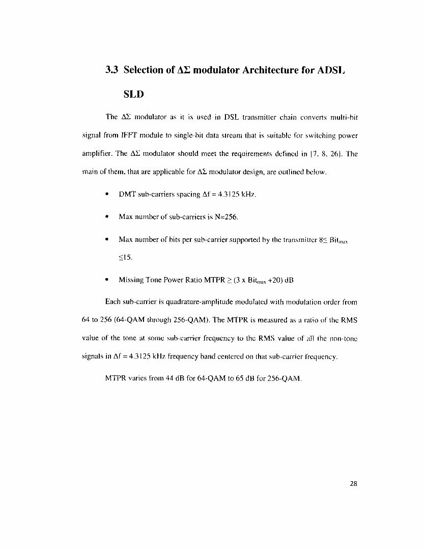
toolbox is depicted in Figure 3.18 below. The maximum load per sub-channel is 12 bits.
To estimate the Missing Tone Power Ratio of the signal at the output of the AS
modulator few sub-carriers in the DMT modulator are disabled. Signal power level at
the "empty" spots is used to estimate the noise due to intermodulation products
produced by the AS modulator. The depth of the cutout in the Power Spectrum Density
function actually represents the MTPR value.
37
50 100 150 203
Sub-channel 250 3J0
Figure 3.18 Bits Loading Distribution
The results of model simulation are shown in Figure 3.19 below.
File Axes Charrels Window Help
5 -100
Frame 6
0.4 0.6 Frequency (MHz)
§kma F3e Axes Channels Window Help
a> .fin
Frame 6 0.4 06
Frequency (MHz)
a) Input Spectrum b) Output Spectrum
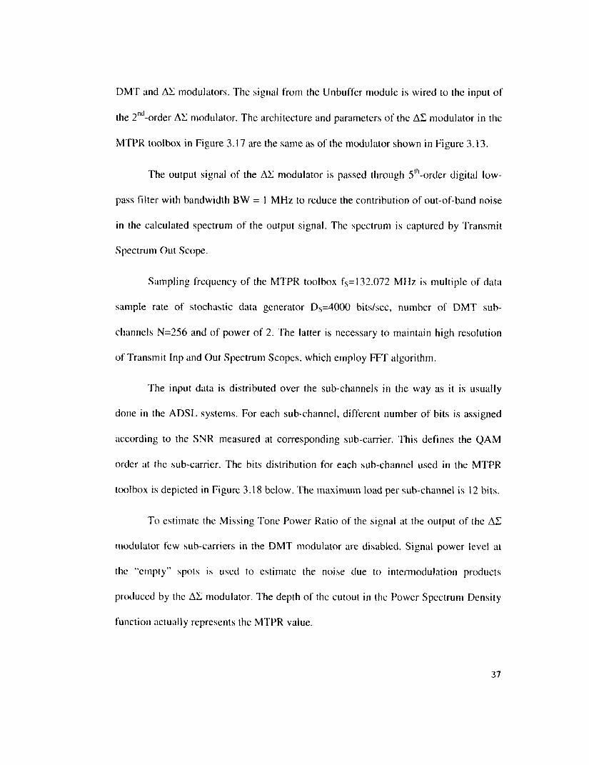
Figure 3.19 Signal Spectra at the Input and Output of 2nd-Order AX Modulator
38

The MTPR value of the signal at the input of the AZ modulator is about 140 dB
(Figure 3.19, a). When the signal is passed through the modulator, the MTPR degrades
to about 65 dB (Figure 3.19, b). This demonstrates the 2nd-order AZ modulator meets
ADSL requirements.
3.4 Conclusion
Matlab/Simulink simulations show that 2n(i-order AZ modulator is suitable as
the data encoder for ADSL line drivers. AZ modulators of higher orders will probably
improve the MTPR value and signal dynamic range. However, implementation of high-
order modulators will certainly bring extra complexity that will definitely jeopardize the
potential benefits of high-order models of AZ modulators.
2nil-order AZ modulator will be used below as the modulator for ADSL line
driver.
39

4 Switching Power Amplifier as a Potential
ADSL Line Driver
Single-bit-output AS modulator is self-sufficient circuitry that can produce the
signal in the format required for the ADSL communication link. The only signal
parameter that might be not matching the relevant specifications is the signal strength.
ITU G.992,1 [7] and G.992.2 [8| documents provide the recommendations for
the ADSL signal power levels at the line terminals. Aggregate power of Central Office
transmitter (ATU-C) should be no more than 20.4 dBm across the whole down-link
bandwidth 138 kHz - 1104 kHz. The power of Customer Premise transmitter (ATU-R)
should be no more than 13 dBm across the up-link bandwidth 25.875 kHz - 138 kHz.
The power levels maintained in the ADSL transmitters are significant for digital
components regardless the technology used to fabricate them.
In case of AL modulator the data to be sent is encoded by signal level transitions
at certain moments of time. Obviously, the power amplifier shouldn't destroy the signal
appearance in time domain. Switching or Class D power amplifiers are the best suited
for such a task. It is worth to note that signal amplitude dynamic range is not a matter of
concern for switching amplifier. The signal amplitude can be recovered at the receiver
side by passive low-pass filter, and so the dynamic range doesn't depend on the
available voltage supply headroom anymore. Of course, the voltage supply defines the
parameters of the circuitry, but in different manner.
40

Standard CMOS inverter with proper transistors dimensions could be a natural
solution for ADSL line driver when AS modulator is used. The inverter as a line driver
amplifier is studied in numerous publications. [3, 29,30] are among them. The authors
investigated potential causes of signal degradation at the output of the inverter when it
is used as an amplifier. The main of them are:
• Power loss due to parasitic capacitances in CMOS devices;
• Large current and high power loss as a result of this when low power supply
voltage is used;
• Large current spikes happening at the moment of signal level switching.
The following discussion addresses these and other issues that appear to be
essential for the subject of this work.
4.1 The Discussion of Class D Power Amplifier
Class D power amplifier is one of the implementations of more generic
switching power amplifier.
Class D amplifier is an electronic circuit where power devices (usually
MOSFETs) are operated as binary switches. The switches are either fully ON or fully
OFF with minimum time spent between these two stages. Regardless the digital-like
mode of operation the amplifiers deal with analog input signals and produce analog
signals at their output terminals. The bandwidth of these signals are usually well below
the switching frequency of amplifier's power devices.
Generic block diagram of Class D power amplifier is given in Figure 4.1 below.
41

irui
Pulse-width Comparator Low-pass Filter Load Modulator Switching Control
and Power Devices
Figure 4.1 Class D Power Amplifier
The amplifier works by generating a square-wave signal with the spectrum,
which low-frequency portion is essentially the wanted output signal. The high-
frequency portion of the spectrum is the result of signal transformation to digital-like
form so the signal can be amplified by switching power devices.
Class D amplifiers are well known for their high efficiency, in particular, in
audio applications. Theoretical power efficiency of Class D amplifier is 100%, if
switching devices are taken into account only. This is because an ideal switch doesn't
contribute to power losses at all. The switch has zero resistance in ON state, and so no
heat is dissipated. In OFF state, the switch conducts no current, and no heat dissipation
takes place again.
Real power MOSFET devices are not ideal switches. Their ON resistance is low,
but not zero, so some signal power is converted in heat. Current leakage takes place in
OFF state of the devices as well. Such switch non-ideality causes some degradation of
the amplifier efficiency.
42

The power efficiency of Class D amplifiers degrades also due to passive low-
pass filter connected to the output terminals of switching power devices. The filter
removes unwanted high-frequency portion of the square-wave signal spectrum to
recover low-frequency signal of interest. As some power is consumed to amplify wide
band signal, filtering out of high-frequency components of this signal after the
amplification brings the power efficiency of the whole unit down. This is regardless the
fact that low-pass filter is usually pure reactive circuit made of inductors and capacitors.
The efficiency degradation due to low-pass filtering can be reduced by increasing the
switching frequency. When the frequency is high enough, high-order signal harmonics
produced by the switching are allocated far away from the main signal component and
have relatively low strength. High switching frequency allows also using low-pass
filters of lower order as their attenuation of high-order harmonics appears to be
sufficient to recover the signal of interest with necessary accuracy.
The practical efficiency of the Class D power amplifiers is around 90% in audio
applications. This is well above theoretical efficiency of Class A, B, AB amplifiers.
4.2 Efficiency of Switching Power Amplifiers with
Matching Circuit
One of the main advantages of switching power amplifier is its high efficiency
mostly due to low ON resistance of output power devices. This might make necessary
to use matching circuit to get maximum possible power transfer from the amplifier to
the communication line.
43
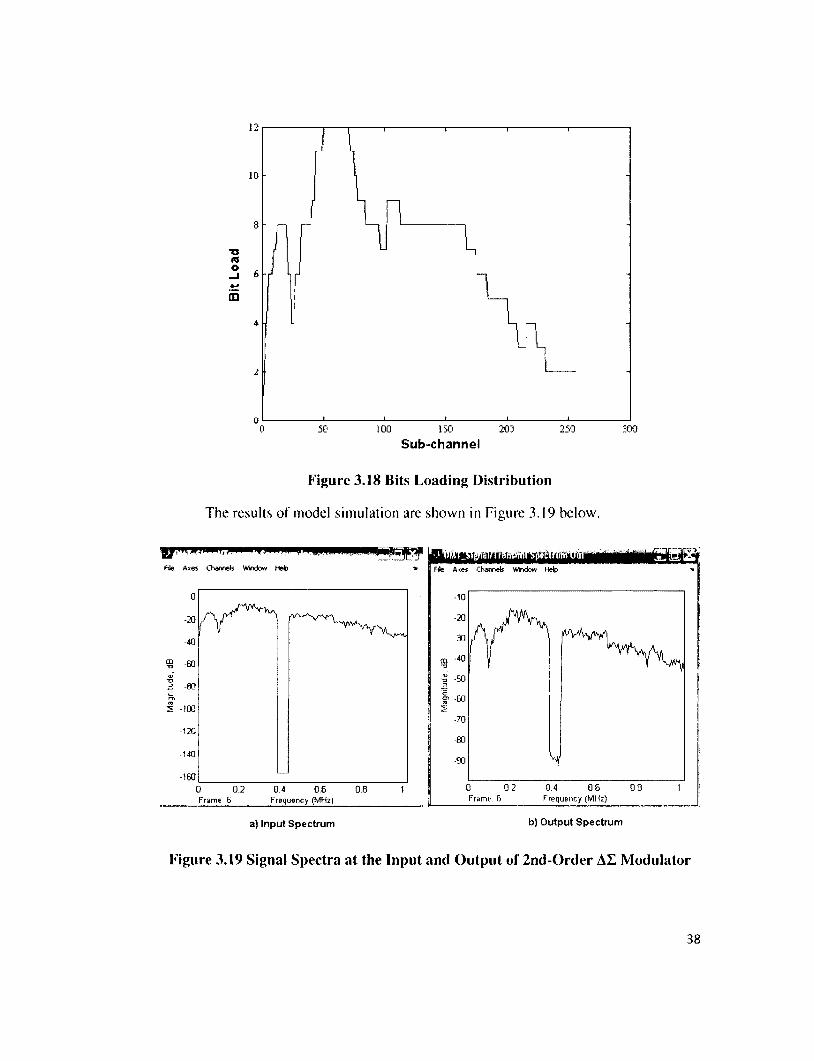
Maximum power transfer theorem, also referred as Jacobi's law, states that, to
obtain maximum external power from a source with finite internal resistance, the
resistance of the load should be equal to the resistance of the source viewed from the
output terminals. The condition of maximum power transfer doesn't result in maximum
efficiency.
v source Rloact oad
1 .
1.0
0 8
04
0 2
Plcad/P n
i ~ / ' ~
R load/ R source
Figure 4.2 Power Transfer Efficiency
If the efficiency is defined as the ratio of power dissipated by the load to
power developed by the source, then it is easy to find out from the circuit in Figure 4.2
that the efficiency can be calculated as follow.
^ ' i< >:'!• (4-1)
Three particular cases can be considered:
r) = 0, when Rkrd{S = 0;
r| = 0.5, when /?|0a(J = /?s,
x] = 1, when /?,oad = co or /?sourcc = 0.
44

The efficiency is only 50% when maximum power transfer is achieved, but
comes to 100% as the load resistance approaches infinity, though the total power level
changes towards zero. Efficiency also approaches 100% if the source resistance is
reduced to zero. All the above applies to resistive (real) component of the power only.
Equivalent electrical diagram of switching power output stage is as follow.
V
R sowce R out
V
R souice Rouf
Figure 4.3 Equivalent Electric Diagram of Switching Amplifier
As one can see in Figure 4.3 above, the output impedance of the amplifier is
equal to:
^ou! = ̂ switch + ^source* (4-2)
where /?Swiich is the ON resistance of the closed switch, Rsouwi: is internal
resistance of power supply. The power supply of the circuit is usually a voltage source,
which has low internal resistance. This means that the output impedance of switching
amplifier is relatively low.
Class D power amplifiers are initially employed for the amplification of audio
signals. The load of audio amplifiers is a speaker with low input impedance. Speaker
impedance is usually from less than one ohm to tens ohms depending on the capacity of
45

the speakers. These values are matching with the output impedance of switching
MOSFET devices in closed state.
One of the key factors that defines the impedance of MOSFET devices in closed
state is the width of active area of the transistors. The devices of higher power capacity
have lower impedance. This relation corresponds, in general, to the relation between the
capacity and input impedance of audio speakers: more powerful speakers have lower
input impedance. Required impedances can be easily calculated, and output-load
matching can be reached even when MOSFET device is connected directly to the
speaker without any impedance transformers. The low-pass filter between them, when
they are used, has usually the same input and output impedances and doesn't affect the
matching at all. This is one of the reasons why no matching circuits are used in audio
applications, and the design of audio power amplifiers are often done to achieve its
maximum efficiency.
In DSL applications the power amplifier should drive the POTS line with
characteristic impedance R\ = 100 Ohm. Such relatively high load resistance makes
necessary to employ matching circuit in between the output of the amplifier and the line
terminals. Equivalent electrical diagram of switching amplifier with matching circuit
can be drawn as in Figure 4.4 below.
The condition of maximum power transfer for the switching amplifier with
matching resistor is as follow.
^source ^switch + ^match ~ ^load (4-3)
46
R souice
Figure 4.4 Switching Amplifier with Matching Resistor
The efficiency of the amplifier shall be:
filcHHl ) ] — (-4.4)
^ load "J" ^sourer ^ r.vit'-ii ^ m .irch
Being the part of power amplifier, the matching circuit will dissipate part of the
signal power. The efficiency of the amplifier is not expected to be more that 50% as per
Jacobi's law.
4.3 Efficiency of Switching Power Amplifiers with Low-
pass Filter
One more consideration should be taken into account when the efficiency of
switching amplifier is being discussed.
Square-wave signals at the input and output of switching amplifier are usually of
the same amplitude. The amplifier produces the signal of higher power, i.e. it injects
more current into load.
47
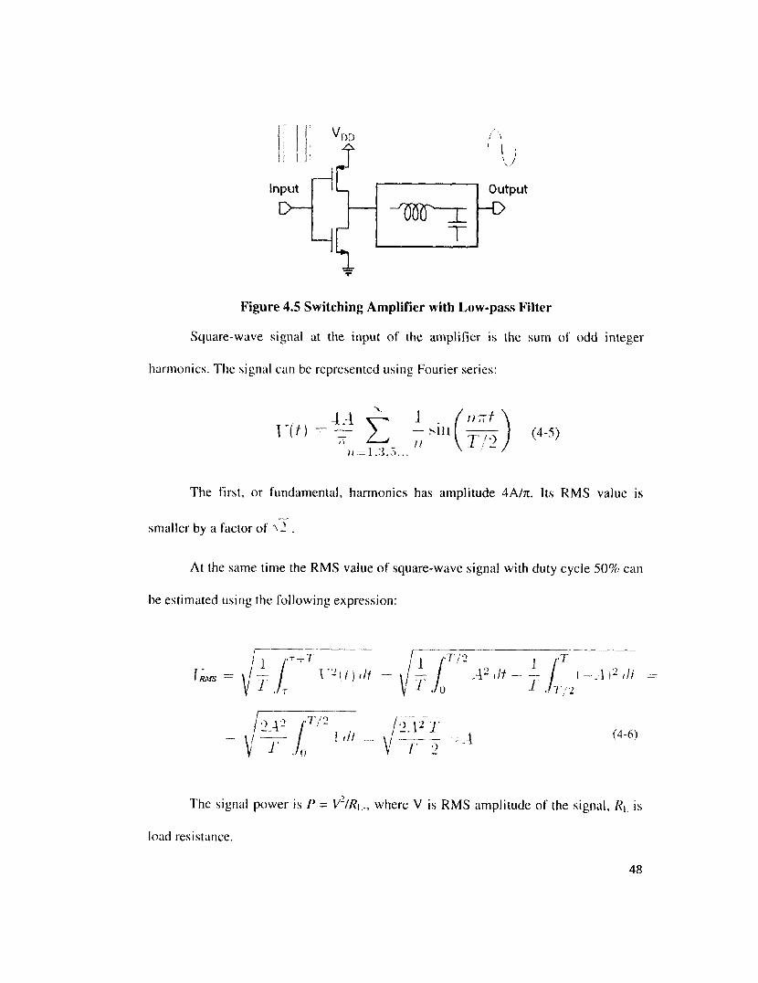
Output
-W-T
Figure 4.5 Switching Amplifier with Low-pass Filter
Square-wave signal at the input of the amplifier is the sum of odd integer
harmonies. The signal can be represented using Fourier series:
4.4 v—* i . (Mat
!'<'> = IT £ TMtF2 n = 1.3.5...
(4-5)
The first, or fundamental, harmonics has amplitude AA/n. Its RMS value is
smaller by a factor of \ 2 .
At the same time the RMS value of square-wave signal with duty cycle 50% can
be estimated using the following expression:
/ , ,-r^T
J RMS — y' J. 1 f T / 2 J rT
i j - 4 2 i I f ; V 1 Jo '1 (—.4 )2 ilt
JTf 2
•14 2
VT
• 7 / 2
hit ./0
/•J.l2 J'
V T 2 •-4 (4-6')
The signal power is P = V7/?i.„ where V is RMS amplitude of the signal, R\, is
load resistance.
48
When switching amplifier is equipped with low-pass filter at the output that
allows the fundamental tone only to pass to load terminal, the efficiency of the amplifier
is as follow.
This shows that the efficiency of switching amplifier with low-pass filter at the
output is at best 81% regardless of the efficiency of the switches.
This conclusion is valid for square-wave symmetrical signal with 50% duty
cycle. The efficiency of the switching amplifier degrades when square-wave signals of
other duty cycle are applied to its input.
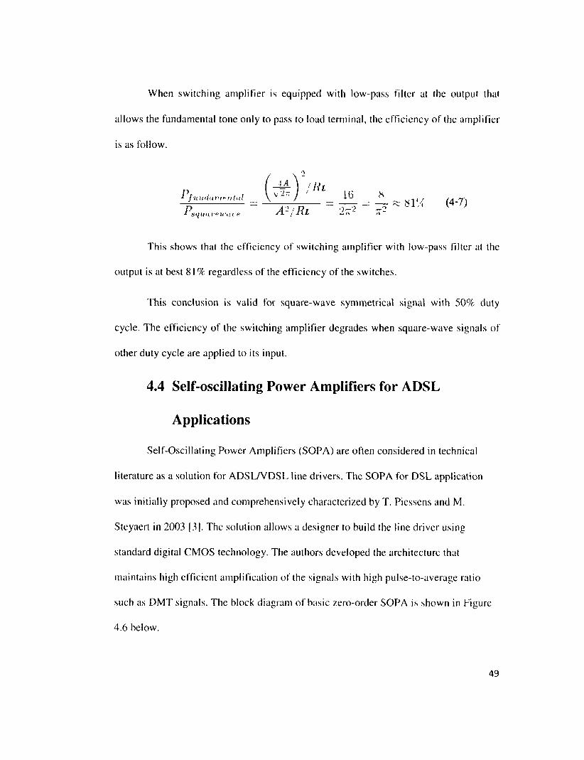
Self-Oscillating Power Amplifiers (SOPA) are often considered in technical
literature as a solution for ADSL/VDSL line drivers. The SOPA for DSL application
was initially proposed and comprehensively characterized by T. Piessens and M.
Steyaert in 2003 (3). The solution allows a designer to build the line driver using
standard digital CMOS technology. The authors developed the architecture that
maintains high efficient amplification of the signals with high pulse-to-average ratio
such as DMT signals. The block diagram of basic zero-order SOPA is shown in Figure
4.6 below.
(4-7)
4.4 Self-oscillating Power Amplifiers for ADSL
Applications
49
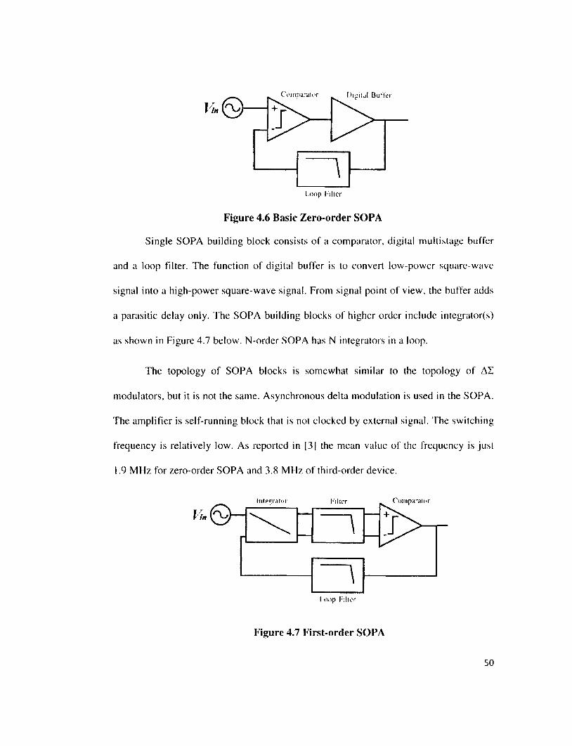
Figure 4.6 Basic Zero-order SOPA
Single SOPA building block consists of a comparator, digital multistage buffer
and a loop filter. The function of digital buffer is to convert low-power square-wave
signal into a high-power square-wave signal. From signal point of view, the buffer adds
a parasitic delay only. The SOPA building blocks of higher order include integrator(s)
as shown in Figure 4.7 below. N-order SOPA has N integrators in a loop.
The topology of SOPA blocks is somewhat similar to the topology of AZ
modulators, but it is not the same. Asynchronous delta modulation is used in the SOPA.
The amplifier is self-running block that is not clocked by external signal. The switching
frequency is relatively low. As reported in [3] the mean value of the frequency is just
1.9 MHz for zero-order SOPA and 3.8 MHz of third-order device.
Figure 4.7 First-order SOPA
50
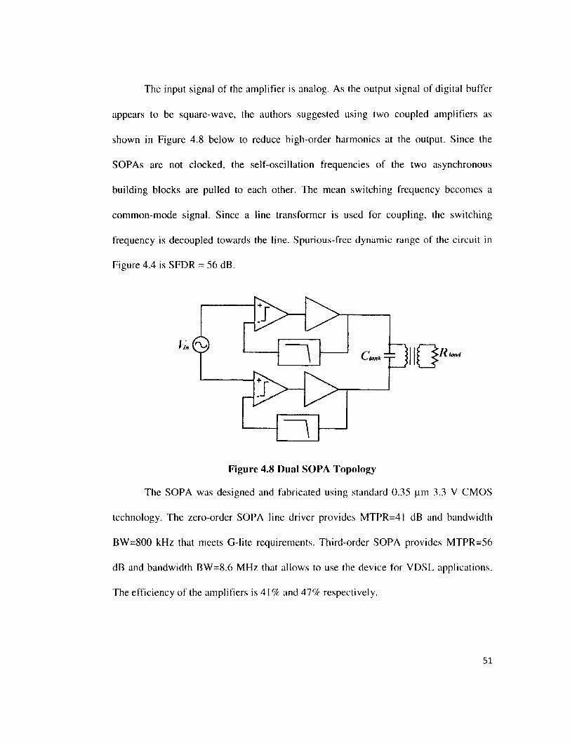
The input signal of the amplifier is analog. As the output signal of digital buffer
appears to be square-wave, the authors suggested using two coupled amplifiers as
shown in Figure 4.8 below to reduce high-order harmonics at the output. Since the
SOPAs are not clocked, the self-oscillation frequencies of the two asynchronous
building blocks are pulled to each other. The mean switching frequency becomes a
common-mode signal. Since a line transformer is used for coupling, the switching
frequency is decoupled towards the line. Spurious-free dynamic range of the circuit in
Figure 4.4 is SFDR = 56 dB.
Ctank
Figure 4.8 Dual SOPA Topology
The SOPA was designed and fabricated using standard 0.35 |jm 3.3 V CMOS
technology. The zero-order SOPA line driver provides MTPR=41 dB and bandwidth
BW=800 kHz that meets G-lite requirements. Third-order SOPA provides MTPR=56
dB and bandwidth BW=8.6 MHz that allows to use the device for VDSL applications.
The efficiency of the amplifiers is 41 % and 47% respectively.
51

4.5 Implementations of Switching Power Devices in
Low-voltage CMOS
Advanced CMOS technologies are characterized by low voltage supply
headroom. This issue poses serious problem for the design of efficient line driver for
DMT signal, which have high PAPR value. The authors in [29] believe that a highly
efficient ADSL line driver in low-voltage CMOS technology is a contradiction. As the
solution, they proposed the SOPA that includes high-voltage output buffer.
The SOPA architecture is proved to be quite successful in digital sub-micron
CMOS since it can drive efficiently the DMT signals with high PAPR value. However,
as with any power amplifier, its efficiency and reliability drop significantly with
decreasing voltage headroom. The authors believe that lowering the supply voltage
results in increased current density to maintain constant output power. This, in turn,
increases hot carrier generation and electro-migration, both of which affect the
reliability of the driver. The large current also results in a drop of efficiency because of
increased switching and conduction losses of the driver. Moreover, the large PAPR
value causes the driver to put signals with high-voltage swing on the line. Since the
output voltage swing of the driver is limited by its supply voltage, a transformer with
high turns ratio should be used. However, this increases the return signal attenuation
that limits the practical use of the line driver.
The proposed solution includes high-voltage buffer as the final stage of the
multistage buffer. The high-voltage buffer is designed in standard submicron CMOS
52
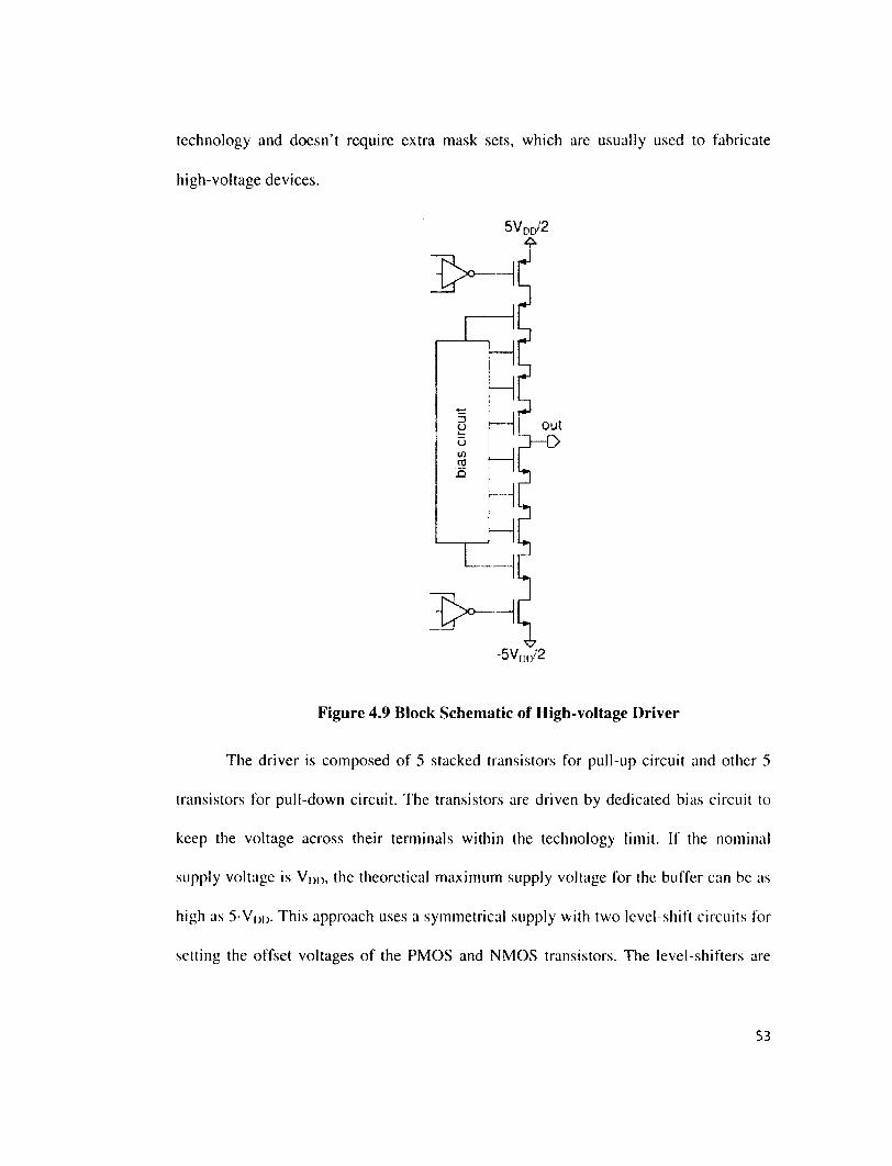
technology and doesn't require extra mask sets, which are usually used to fabricate
high-voltage devices.
The driver is composed of 5 stacked transistors for pull-up circuit and other 5
transistors for pull-down circuit. The transistors are driven by dedicated bias circuit to
keep the voltage across their terminals within the technology limit. If the nominal
supply voltage is VDD, the theoretical maximum supply voltage for the buffer can be as
high as 5 V|)d. This approach uses a symmetrical supply with two level-shift circuits for
setting the offset voltages of the PMOS and NMOS transistors. The level-shifters are
5Vdd/2
Figure 4.9 Block Schematic of High-voltage Driver
53

preceded by non-overlapping switching circuit to avoid short-circuit currents that can
cause significant power dissipation at high voltages.
The driver was fabricated and tested with nominal power supply voltage V»i) =
1.2 V. The high-voltage driver operated at supply voltage V = 5.5 V. When 512-tone
DMT signal is applied to the input of the SOPA with high-voltage driver, Missing Tone
Power Ratio is MTPR = 58 dB with an average output power 20 dBm. These
parameters allow using this device for ADSL2 applications. Measured efficiency of the
driver is 42%.
The stacked output stage is attractive from a cost point of view as it is
implemented entirely with low-voltage devices, but its complexity makes it too slow for
wide band systems (8 MHz and higher). [30] offered similar to the above SOPA
architecture [29] with separate core low-voltage and driver high-voltage power supply,
but developed new fast output stage. The output stage is implemented with NMOS
devices only. This reduces by two the driven gate area compared to traditional
NMOS/PMOS totem pole and so maximizes the switching frequency, minimizes
switching losses and reduces the power consumption of the driver. Simulation showed
that the bandwidth of the line driver is about 30 MHz, which is much higher than the
bandwidth BW=2.2 MHz of the line driver [29]. However, the price paid to get this
improvement is significant. The MTPR reduced to 31 dB and the efficiency dropped to
23 % only.
54
4.6 Switching Output Buffer with Wideband
Transformer
Stacked output stage with voltage supply, that is higher than core logic voltage,
allows getting required output power with lower drain current. Such exchange of higher
current for higher voltage is not always necessary. Reliability degradation due to hot-
carrier generation and electro-migration takes place because of high current density.
However, current density can be maintained at reasonably low level in CMOS
transistors, while the drain current through this transistor can be as high as necessary to
obtain required output power. This is clear from the expression that defines the current
through the transistors. The current depends, among other parameters, on the width of
the active channel (or the width of gate terminal) that can be made as big as necessary.
In triode (ohmic) mode, drain current /» of NMOS transistor is as follow:
where Vm and Vqs are voltage drops between drain and source and between gate
and source terminals respectfully, V,/, - threshold voltage, f.i„ is charge-carrier mobility
(electrons here), Cox is gate oxide capacitance per unit area, L and W are length and
width of gate terminal. Similar expression exists for the PMOS transistor.
If current density can be maintained at reasonably low level by selecting proper
width of the transistor channel, the standard PMOS/NMOS totem pole can be used to
build the output buffer of the line driver. As the driver should manage relatively high
current to provide required signal power at the line terminals, the internal resistance of
(4-8)
55

the buffer (or switching circuit) should be low enough. This means that the line driver
should include impedance transformer and matching circuit. The block diagram of
CMOS buffer with associated circuitry is shown in Figure 4.10 below.
Figure 4.10 Output CMOS Buffer with Impedance Transformer and LPF
The necessity to have impedance transformer is defined by low-voltage power
supply of CMOS buffer. To get the output power Pout = 20 dBm at power supply V =
2.5 V the current through the transistor should be I = PQUT/V = 40 mA. The output
impedance of the circuit should be R = 62.5 Ohm minimum to provide required output
power. As the CMOS buffer should work as the switch, its internal resistance in ON
state should much smaller than R = 62.5 Ohm. It is not realistic to assume that CMOS
transistors behave as an ideal switch, but RON = 3-5 Ohm resistance value would be
acceptablc. This will allow keeping the passive power dissipation in PMOS/NMOS
totem pole low enough. Of course, the size of the transistors is going to be large to
maintain the current density within technological range.
Push-pull circuit shown in Figure 4.10 above is known in technical literature as
half H-bridge driver. CMOS transistors of the output buffer switch the load either to the
Inpt
D Impedance Transformer
Matching Circuit
LPF —[>
Output
56
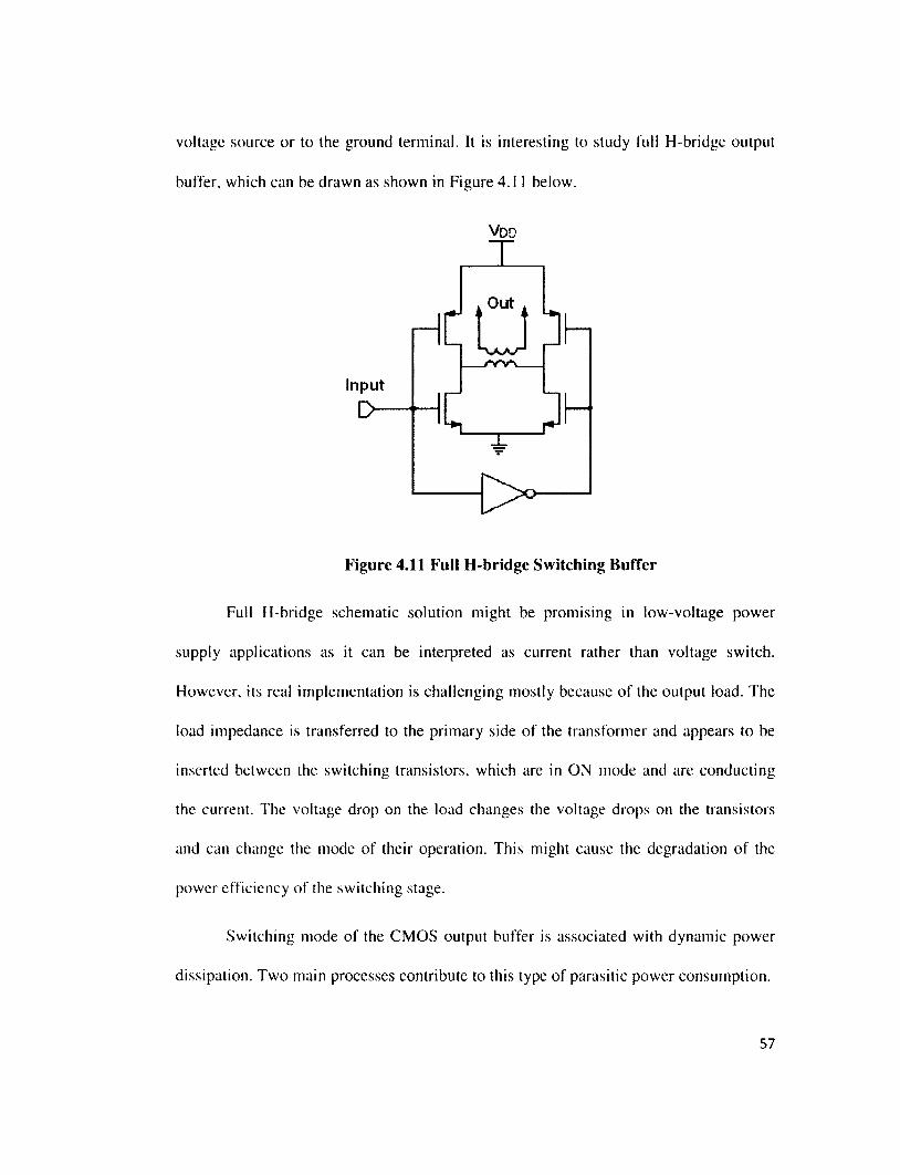
voltage source or to the ground terminal. It is interesting to study full H-bridge output
buffer, which can be drawn as shown in Figure 4.11 below.
Vdd
Full H-bridge schematic solution might be promising in low-voltage power
supply applications as it can be interpreted as current rather than voltage switch.
However, its real implementation is challenging mostly because of the output load. The
load impedance is transferred to the primary side of the transformer and appears to be
inserted between the switching transistors, which are in ON mode and are conducting
the current. The voltage drop on the load changes the voltage drops on the transistors
and can change the mode of their operation. This might cause the degradation of the
power efficiency of the switching stage.
Switching mode of the CMOS output buffer is associated with dynamic power
dissipation. Two main processes contribute to this type of parasitic power consumption.
In
x
Figure 4.11 Full H-bridge Switching Buffer
57

CMOS circuits dissipate power by charging/discharging the various node/load
capacitances (mostly gate and wire capacitance, but also drain and source capacitances)
whenever they are switched. In one complete cycle of CMOS logic, current flows from
Vdd to the load capacitance Q. to charge it and then flows from the charged load
capacitance to ground during discharge stage. Therefore, in one complete
charge/discharge cycle, a total charge Qsw=Q VDD is transferred from VDD to ground.
Leakage current is the product of the charge Qsw multiplied by the switching frequency
fsw:
Isw = Qsw-fsw (4-9)
The power dissipated by CMOS device due to the switching is:
P = Isw-VDD = Ci.-Voi/fsw (4-10)
If the load capacitance is estimated on a node together with average switching
frequency, the dynamic power dissipation at that node can be calculated effectively. As
one can see, dynamic power dissipation due to the switching is higher with high
node/load capacitances, which rise when the dimensions of the node/load gets larger. It
is worth to note that it is beneficial to use low-voltage power supply, as the switching
loss increases when Von goes up.
The second process that contributes to the dynamic power dissipation is so-
called short-circuit power dissipation. Since there is a finite rise/fall time for PMOS and
NMOS devices, both transistors can be ON for a short moment of time during transition
from one state to the other. Some current will flow from V^o directly to ground, hence
58

creating a short circuit current. Short circuit power dissipation increases with rise and
fall time of the transistors.
An additional mechanism of power consumption became significant in advances
CMOS technologies as wires on chip became narrower, and the long wires became
more resistive. CMOS gates at the end of those resistive wires see slow input
transitions. During the middle of these transitions, both the NMOS and PMOS logic
networks are partially conductive and current flows directly from V^u to Vss- The
power thus wasted is called crowbar power and similar to short-circuit power
dissipation. Careful design, which avoids weakly driven long skinny wires, can
ameliorate this effect, and crowbar power can be done substantially smaller than
switching power.
4.7 Conclusions
This section begins with review of Class D power amplifiers that are well
known for their high efficiency in audio applications. The main component of Class D
power amplifiers is switching output stage, which dissipates very small amount of
power.
The switching amplifiers were studied as the line drivers in DSL applications.
Surprisingly, but the available publications report of relatively low, 50% or less,
efficiency of switching output buffers. The authors believe that the degradation of the
driver's efficiency takes place because of high PAPR value of the signal. They state that
it is difficult to amplify such signal when voltage supply headroom is limited. This
explanation is reasonable to some extent, although the losses due to the matching
59

circuits, dynamic power dissipation and, potentially, low-pass filtering should be taken
into account as well.
It seems strange, but no design solutions are published on the DSL line drivers
that use AX modulator as data encoder for switching output buffer. The architecture of
the line driver with AL modulator doesn't require traditional Class D power amplifier
with analog input and analog output. The output of the AS modulator is single-bit data
stream, or two-level digital like signal. When such encoder is employed, the power
amplifier should just pump certain amount of energy to the output terminals without
changing the shape of the signal.
Preliminary study reveals that generic push-pull NMOS/PMOS totem pole
might be good enough as a switching line driver for DSL applications, however, the
final decision should be made based on simulation results and following testing of real
fabricated device in a lab.
It is not expected that the efficiency of the line driver will be as high as it is for
audio Class D power amplifiers. Higher frequency bandwidth of DSL signals increases
the power loss due to such things as matching and dynamic power dissipation that are
not essential in audio applications.
60

5 ADSL Switching Line Driver with AL
Modulator
The design of the ADSL line driver that consists of the sigma-delta modulator
followed by the switching amplifier is studied below. The architecture has been
discussed in internet community, but no real technical solutions are proposed in
professional publications.
The line driver is designed as a completely digital device. Such approach is
innovative, in particular, when AS modulator is considered. Most AS modulators,
especially, of 2nd-order and higher, are made as the analog devices as per known
publications. It is very appealing to build the device using digital technique only as the
digital design gets the advantages of modern advanced CMOS technologies. It also
seems to be logical for transmission path as the input signal for the line driver is
generated by IFFT signal processor, which is always implemented as digital device.
Removing digital-to-analog and following analog-to-digital conversions will
supposedly improve the performance of the device.
The line driver is composed of AS modulator, connected in series to the
switching amplifier. This topology allows splitting the design for two relatively
independent steps. The AS modulator is designed as RTL code in Verilog HDL that can
be easily captured in schematic using well known tools from Altera, Xilinx, Synopsis
and others available on the market. The switching amplifier is designed with Cadence
61
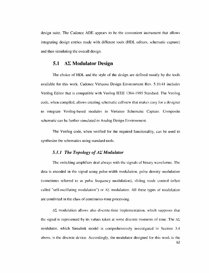
design suite. The Cadence ADE appears to be the convenient instrument that allows
integrating design entries made with different tools (HDL editors, schematic capture)
and then simulating the overall design.
5.1 AL Modulator Design
The choice of HDL and the style of the design are defined mostly by the tools
available for this work. Cadence Virtuoso Design Environment Rev. 5.10.41 includes
Verilog Editor that is compatible with Verilog IEEE 1364-1995 Standard. The Verilog
code, when compiled, allows creating schematic cellview that makes easy for a designer
to integrate Verilog-based modules in Virtuoso Schematic Capture. Composite
schematic can be further simulated in Analog Design Environment.
The Verilog code, when verified for the required functionality, can be used to
synthesize the schematics using standard tools.
5.1.1 The Topology of AE Modulator
The switching amplifiers deal always with the signals of binary waveforms. The
data is encoded in the signal using pulse-width modulation, pulse density modulation
(sometimes referred to as pulse frequency modulation), sliding mode control (often
called "self-oscillating modulation") or AI modulation. All these types of modulation
are combined in the class of continuous-time processing.
AS modulation allows also discrete-time implementation, which supposes that
the signal is represented by its values taken at some discrete moments of time. The AI
modulator, which Simulink model is comprehensively investigated in Section 3.4
above, is the discrete device. Accordingly, the modulator designed for this work is the
62
discrete device. The model of AS modulator, which is used to design the Verilog code
of the device, is shown in Figure 5.1 below.
0.5
Adder 1 Adder 2 Ideal Integrator 1
0.5
Ideal Integrator 2 Re'ay
Figure 5.1 2nd Order Sigma-Delta Modulator
The simulations showed that the performance of the AL modulator is very
sensitive to the value of its internal parameters. The parameters define the loopback
gain of the device and the distribution of feed-forward gain from its input to the output.
It is found that the best performance of the modulator takes place if the gain of each of
its two stages is equal. Also for better performance the proportion of feed-forward
signal and loopback signal at the input of adder modules should be equal for both
modules in the model. The relation between the saturation level of the Ideal Integrators
and signal amplitude of Relay module strongly affects the signal-to-noisc ratio at the
output of the AI modulator as well. Certainly, the optimal set of the model parameters
can be justified theoretically, if it is not done already.
It is worth to note that the quantitative relations of the parameters of the AI
modulator designed for this work in Verilog HDL completely correspond to their
counterparts of the Simulink model.
63

The discrete nature of the AS modulator defines its distinctive feature when the
modulator is built as a pure digital device. The execution of the functional operation
within each modulator's module should be completed in one sample/clock period or
less, so that the signal change at the input of the module and corresponding signal
change at the output take place within one clock period. This actually means that the
signal propagation delay within each module of the AS modulator should be less than
the clock period.
The feasibility of such requirement is defined by the CMOS technology used to
fabricate the device. 0.18 |4.m CMOS is supposed to be suitable. This technology allows
designers to fabricate reasonable fast and relatively low-voltage devices, which might
be no such expensive compared to more advanced silicon technologies. The detailed
discussion of the relevant features of 0.18 |nm CMOS is provided below.
The signal propagation delay in the modules of the digital AS modulator is
functionally similar to the slew rate of the operational amplifiers that are the parts of the
legacy analog AI modulators. The slew rate strongly affects the performance of the
analog AS modulators that are built with switched-capacitor integrators. Similarly, in
digital modulators large propagation delays can completely destroy the signal
transformation along its whole path from the input to the output of the device.
The constraint on the module's propagation delay is very critical for the Ideal
Integrator module of the AS modulator. The modulator includes two Ideal Integrators,
which define the order of the AS modulator and, accordingly, its performance. The
functional block diagram of the integrator is shown in Figure 5.2 below.
64

Sample
Adder Saturation Unit Delay
Figure 5.2 Functional Block Diagram of Ideal Integrator
The integrator operates properly when the overall delay of its Adder and
Saturation blocks are less than one sample period. The Unit Delay block of the Ideal
Integrator makes the total signal propagation delay of the integrator equal to one sample
period. If this is the case, the integrator behaves as required. If the total signal
propagation delay of the integrator is more than one sample period, the performance of
the digital sigma-delta modulator can change in unpredictable manner.
The signal propagation delay of the modules composing the digital sigma-delta
modulator is different. As the digital implementation of the operations performed by the
modules are known, the signal propagation delay in the modules can be estimated in
quite a reasonable manner. For this purpose the number of gates, which the signal
should go through within each module, shall be determined. The delay of the gate for
particular CMOS technology is usually known. It is specified in the libraries of standard
cells developed for that technology. For 0.18 pm CMOS the gate delay (2-input NAND,
fanout =2, internal gates) is reported to be from 39 ps (Fujitsu 6-metal CS80A process,
(311) to 43.6 ps (6-layer interconnect process, Epson S1L70000 Series Gate Arrays,
65

132]). Similar gate delays have been demonstrated by the ring oscillators built with
TSMC 0.18 urn 1P6M CMOS technology.
The value t(> = 45 ps shall be used below as the propagation delay of standard
NAND gate built with 0.18 pm CMOS technology. The propagation delay in each
module of the AS modulator is estimated as the gate delay multiplied by the number of
gates in the longest signal path in the module.
The amplifier with the gain G=0.5 is actually the divider by two. This operation
corresponds to shifting the whole digital word/code by one bit to the left. The
implementation of the logical shift is simple: bit N of the input word/code is wired to bit
N-l of the output word/code. The most significant bit of the output code is always equal
to logical zero. The operation doesn't require any digital processing and implemented
by proper signal wiring. The delay of such operation is insignificant and can be ignored
at all.
The saturation operations in the Ideal Integrator and Relay modules require
some processing. The processing algorithm can be represented by the schematics shown
in Figure 5.3 below. The schematic is quite simple and allows estimating the
contribution of the saturation blocks of the Ideal Integrator and Relay blocks in the
signal propagation delay.
66

NAND BitN
NAND Bit N-1
Word 1
NAND Bit 1
NAND BitO NAND
NAND NAND Word 1, BitN NAND
NAND NAND
NAND
NAND BitN
NAND Bit N-1
Word 2
NAND Bit 1
NAND BitO
Figure 5.3 Saturation Schematics
The most critical path is made of the RS latch followed by two gates connected
in series. The total number of gates that signal should pass through is four.
The adder blocks make the largest contribution in the signal propagation delay.
Different architectures of the adder blocks are known. The ripple carry adder, being
simple in concept, has a long circuit delay due to the many gates in the carry path from
the least significant bit to the most significant bit. For a typical design, the longest delay
67
path through an n-bit ripple carry adder is 2n+2 gates. Thus, for the 16-bit adder the
longest path that the signal goes through includes 34 gates. The carry look-ahead adder
is the alternative solution. This adder has the architecture with reduced critical signal
path at the price of more complex hardware. In 16-bit carry look-ahead adder the
longest signal path includes 10 gates only [33].
The width of the signal word should be defined in order to estimate the
propagation delay of the modules of the AS modulator. As specified in [261, the
maximal number of bits per sub-carrier supported by ADSL transmitter is 8< Bitmax <15.
This means that the signal level should be maintained by 16-bit data format as a
minimum. Wider data format would be desirable to reduce the quantization error;
however, this introduces the extra delays in the modulator's modules that might cause
essential degradation of the modulator's performance.
As mentioned earlier, excessive delays in the digital modules of AS modulator
cause unwanted SNR degradation at the output of the modulator and, as a result, the
reduction of its dynamic range. The digital circuits with large delays are unable to react
on the fast signal variations that might happen during the transitional time of digital
device. As a result, signal distortion takes place. This effect is similar to the signal
clipping in analog devices. The fast changing signals with high PAPR, such as DSL
signals, are particularly vulnerable to such effect.
The AS modulator is designed for 16-bit signal width. The number of signal bits
might be increased only if the performance of the ADSL line driver doesn't meet the
relevant specifications.
68

The modules' delays of the 16-bit AE modulator are given in Table 1 below.
Table 1 A£ Modulator's Modules Delay
Module No of gates in the
critical path Delay
Adder 1 10 450 ps
Ideal integrator 1 10+4 630 ps
Adder 2 10 450 ps
Divider by 2 1 45 ps
Ideal integrator 2 10+4 630 ps
Relay 4 180 ps
Divider by 2 1 45 ps
The Simulink model of the AX modulator has been studied with the sample
period Ts = 7.8125 ns (sample frequency fs = 128 MHz). The sample period is 10 times
larger than the maximum delay observed in the modules of the AS modulator provided
it is designed with 0.18 |jm CMOS. This allows to build the modulator, which
performance is not degraded due to the technology restrictions.
5.1.2 Verilog Modules
The AS modulator is designed as a set of modules of the same hierarchy.
Cadence Verilog compiler generates the schematic symbol upon successful code
compilation of each module. The Verilog module symbols can be integrated with the
schematics of the switching amplifier for further simulation.
69

Unsigned arithmetic is used to simplify the schematic implementation of Verilog
modules during synthesis. The unsigned arithmetic is possible when the DC offset is
added to the signal propagating in the AS modulator.
The signal at the input of the modulator has the offset equal to the half of its
total range. This offset level corresponds to zero voltage level for an analog signal
propagating inside of the AS modulator without DC offset. Switching signal polarity in
unsigned arithmetic with half-range signal offset corresponds to changing the most
significant bit from one logic level to the other one. The determination of the signal
polarity in HDL conditional operands can be done easily by checking the value of the
most significant bit of signal word only. This definitely reduces the corresponding
electronics
Similarly, minimum and maximum of the signal at the output of ideal integrators
inside the AS modulator are limited to the levels that are defined by two most significant
bits of the signal words, 11000..00 and 01000..00. This makes necessary to check these
two bits only in HDL conditional operands and so to reduce the signal delays in
corresponding hardware modules due to less electronics. The signal extremes at the
output of the integrators are equal to ± 50% of total signal range.
11111111
11000000 10000000 01000000
00000000
2 N
1-0
Figure 5.4 Signal Code Space
70
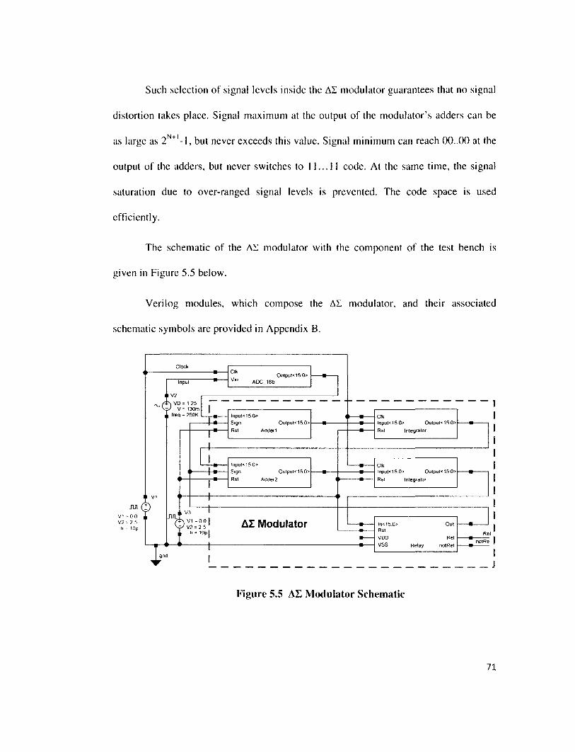
Such selection of signal levels inside the AS modulator guarantees that no signal
distortion takes place. Signal maximum at the output of the modulator's adders can be
as large as 2N+I-1, but never exceeds this value. Signal minimum can reach 00..00 at the
output of the adders, but never switches to 11...11 code. At the same time, the signal
saturation due to over-ranged signal levels is prevented. The code space is used
efficiently.
The schematic of the AS modulator with the component of the test bench is
given in Figure 5.5 below.
Verilog modules, which compose the AS modulator, and their associated
schematic symbols are provided in Appendix B.
JUL©
Input
I V2
VD = 1 25 V - 130m
I freq = 250K
Clk
Vin 0u*put<150>
Vt - 00 V2 ^2 5
tr - lOp
JUIT
f v i = 0 0 V2 = 2 5 tr = I0p
gnd
Input<l5 0>
Sign 0utput<15:0>
Rst Adderl
Input<15 0>
Sign 0utput<!50>
Rst Adder2
AZ Modulator
Clk lnput<15 0> Output< 15 0>
Rst Integrator
Clk lnput<15 0> 0utput<15:0>
Rst Integrator
ln<15.0> Out Rst
VDD Rel
VSS Relay notRel
Figure 5.5 AD Modulator Schematic
71

5.2 Switching Amplifier Design
As discussed in Section 4, the switching power amplifier made of generic
CMOS inverters is one of the most effective and easy solutions for ADSL line driver.
Both half-bridge or full-bridge configurations of the line driver are studied and
compared below.
The main parameter of the inverter is the size of the CMOS devices of totem-
pole transistor pair. The size is defined mostly by the technology used to fabricate the
circuitry.
The selection of the CMOS technology for the switching power amplifier is
somewhat intuitive. The following considerations are taken into account:
• The circuitry should be able to operate with the clock frequency up to 260
MHz;
• The standard voltage supply should be high enough to avoid too high
current in the output NMOS/PMOS totem pole;
• Technological current density limit should be high enough to withstand the
required current;
• The transistor geometry should be small enough to avoid the clock
frequency reduction due to too large parasitic capacitances.
The most reasonable choice for the switching power amplifier is the CMOS with
0.1 S^m minimum geometry size. The advantages of 0.18p.ni CMOS as related to the
switching power amplifier for ADSL applications are as follows:
72

• Maximum clock frequency could be as high as 3 GHz [34) for the standard
transistors size used in digital applications;
• Recommended power supply voltage covers 1.8-3.3 V range that gives
some freedom for a designer;
• The power supply voltage is high enough that allows to maintain low
current in the transistors;
• Maximum allowed current density (1mA/ fj.m for metal lines and 0.28 mA/
jim for vias/contacts) is high enough to withstand the expected currents with
minimal possible transistor size.
The actual maximum toggle frequency of the inverter in the switching power
amplifier is expected to be much lower than 3 GHz because of relatively large transistor
size. Parasitic capacitances of the large transistors are larger than of the small ones. This
causes the toggle frequency to drop. The actual maximal frequency of the inverter with
the transistors of some specific size can be estimated in the circuit simulation.
The supply voltage headroom that is possible in 0.18 [.im CMOS is not high
enough to deliver lOOmW power into R=100 Ohm load, even when maximum power
supply voltage Vdd = 3.3 V is used. The voltage/impedance transformer can be inserted
in front of the load terminals as shown for the half-bridge amplifier architecture in
Figure 5.6 below.
73

Vdd
RMATCH Transformer
Figure 5.6 Functional Block Diagram of Switching Amplifier with Connected Load
In the block diagram RMATCH includes ON resistance of the switch and internal
resistance of the power supply.
As per Jacobi's law, the output impedance Rout should be equal to the load
impedance RLOAD TO obtain maximum power on RLOAD from the source.
Without the transformer RMATCH should be equal to RLOAD =100 Ohm.
Maximum current that can be developed in the load is IMAX = VSs/( RI.OAD + RMATCH)-
When VDD= 3.3 V is used, IMAX = 16.5 mA. Accordingly the power in the load is
27.225 mW, which is lower then W = 100 mW required for ADSL line driver at CO
location.
When the transformer is used, the requirement for the supply voltage headroom
can be relaxed. With transformer ratio of secondary coil turns N,s to the primary coil
turns N]> N = Ns : Np = 3:1, the load, when looked from the primary side of the
transformer, has resistance RLOAD = 100/N2 = II Ohm only. Accordingly, RMATCH
74

resistor is reduced to this value also. With Von as low as 2.5 V, Imax's as high as 114
mA, and the power in the load is 140 mW.
As noted above RMATCH includes the internal resistance RON of the CMOS
transistor, either PMOS or NMOS, in open state. RON is fixed and depends on the size
of the transistor. The transistors of the switching amplifier are expected to be of
relatively large size in order to get low internal resistance and high-power output signal.
The final stage of the switching amplifier is preceded by two preliminary amplification
stages with the transistors of smaller sizes. The transistors of the preliminary stages
develop the signal to the certain power level and thus allow maintaining the rise and fall
times of the pulses at the gates of the last amplifier stage short enough. The transistor
sizes of first two stages are not optimized to get the minimum delay because the delay
doesn't affect the overall performance of the line driver. The schematic of the switching
power amplifier of half H-bridge architecture is given in Figure 5.7 below.
' M1
pch'
1-180 OOn w=3u
Up1
M2
"nch"
1=180 OOn w=1 3u
M3
"pch"
1=180 OOn w=3u
M4
"nch"
1=180 OOn w=1 3u
' M5
"pch'
1=180 OOn w=39u
Up3
^/VW
1=180 OOn w=12 18u
gnd
Figure 5.7 Half H-bridge Switching Amplifier Schematic
75

The simulations of switching power amplifier revealed that the signal output
power is quite sensitive to the matching conditions. There are three parameters in the
schematic above that affect the matching, namely, transistor's internal impedance RON,
matching resistance RMATCH and transformer ratio N. RON value depends mostly on the
dimensions of the transistors, but it is also influenced by the latter two parameters.
Indeed, the transistor impedance in open state can be roughly estimated as RON =
Vds/Id, where VDs is the voltage drop between the source and drain terminals of the
switching transistor, ID is the current flowing through it. The current through the
transistors depends on VDS voltage drop between drain and source terminals. The
voltage is defined, first of all, by the power supply voltage. Also, the VDS value in the
circuit in Figure 5.6 above depends on the voltage drop on RMATCH and RI.OAD resistors.
VQS = VRD - ID (RMATCH + RLOAD/N') (5-1)
As a result, it is practically impossible to make the preliminary estimations of
the transistors dimensions and the values of the passive components around them. The
circuit simulation is more effective way to determine the parameters of its components.
This allows getting the transistors of minimal possible size while having maximum
possible current through them.
It is worth to note here that the matching resistor helps to reduce the fluctuations
of output signal due to the variations of the power supply voltage. When the voltage
goes up, the current through the NMOS/PMOS transistors increases. This causes
increasing the voltage drop on the matching resistor that reduces V|>s voltage and brings
ID current down.
76

The simulations are done to determine the best matching conditions with
matching resistors RMATCH = 0, 2 and 3 Ohms for the circuit that provides the signal of
no less than 100 mW peak power at the line terminals. The results are summarized in
Table 2 below.
Table 2 Half H-bridge Switching Amplifier
RMATCH, PMOS Transistor NMOS Transistor Transformer POUT,
|Ohm| Size, |(jm] Size, [|im] Ratio |mW]
0 L = 0.180 L = 0.180 41 : 10 104.5
W = 780 W = 250
2 L = 0.180 L = 0.180 -t*
00
o
100.8
W= 1260 W = 392
3 L = 0.180 L = 0.180 o
o
100.1
W = 2340 W = 672
The relative sizes of the PMOS and NMOS transistors are adjusted in order to
get the same values of RON internal resistances of NMOS and PMOS transistors in the
open state. This equalizes the fall and rise times of the pulses propagating in the
switching amplifier.
The rise and fall times of the pulses in between the stages and at the output of
the amplifier in Figure 5.7 with RMATCH = 2 Ohm don't exceed 1.2 ns. This means that
the amplifier can be used with the switching signal of up to 400 MHz.
77
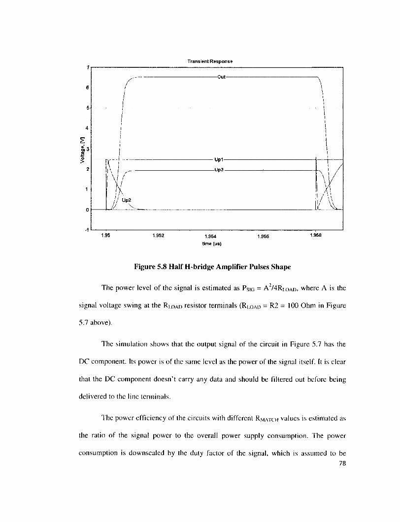
7
6
5
4
s SI 3 10 *•*
o >
2
1
0
-1
1.95 1.952 1.964 1,956 1958
time (us)
Figure 5.8 Half H-bridge Amplifier Pulses Shape
The power level of the signal is estimated as PSIG = A2/4RI.OAD, where A is the
signal voltage swing at the RI.OAD resistor terminals (RI.OAD = R2 = 100 Ohm in Figure
5.7 above).
The simulation shows that the output signal of the circuit in Figure 5.7 has the
DC component. Its power is of the same level as the power of the signal itself. It is clear
that the DC component doesn't carry any data and should be filtered out before being
delivered to the line terminals.
The power efficiency of the circuits with different RMATCH values is estimated as
the ratio of the signal power to the overall power supply consumption. The power
consumption is downscaled by the duty factor of the signal, which is assumed to be
78
Transient Response
-Out-A
L i\ i •
i / K // Up2 J V.
Up1-
-Up3-
\ /
\V /• !
f , / \ \ 1 / \ v 1/ Vv.
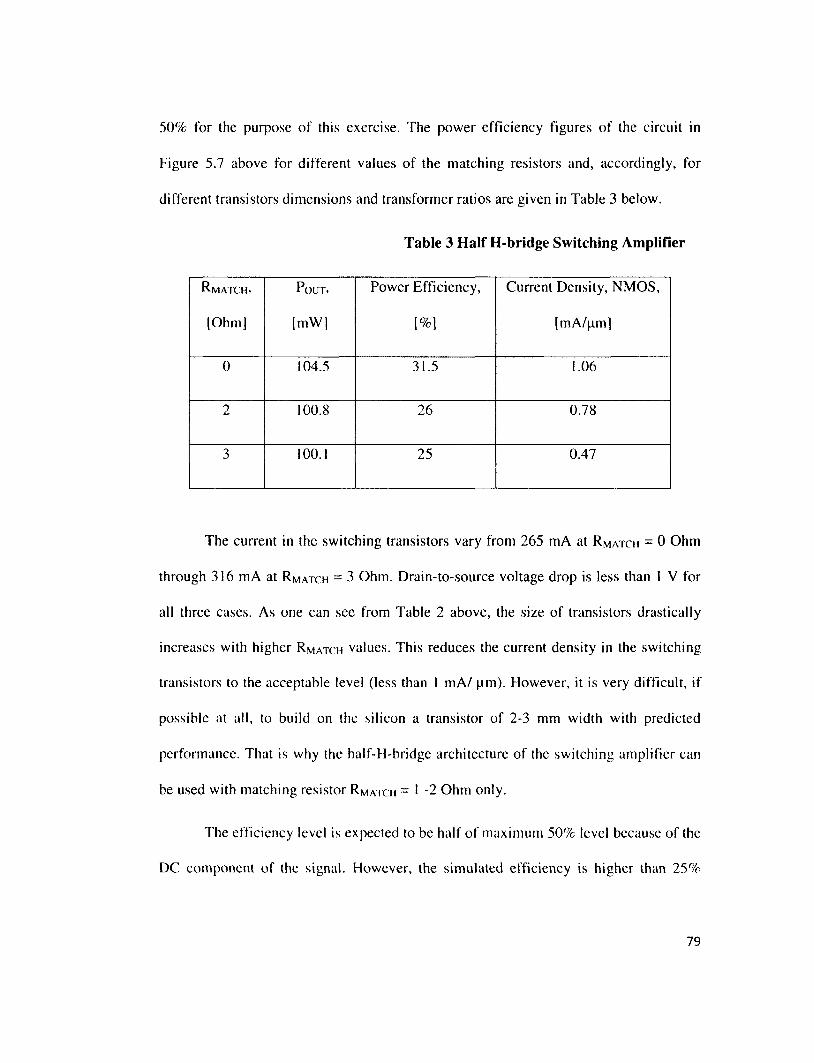
50% for the purpose of this exercise. The power efficiency figures of the circuit in
Figure 5.7 above for different values of the matching resistors and, accordingly, for
different transistors dimensions and transformer ratios are given in Table 3 below.
Table 3 Half H-bridge Switching Amplifier
RMATCH, POUT. Power Efficiency, Current Density, NMOS,
[Ohm] |mW] [%1 [mA/pm]
0 104.5 31.5 1.06
2 100.8 26 0.78
3 100.1 25 0.47
The current in the switching transistors vary from 265 mA at RMATCH = 0 Ohm
through 316 mA at RMATCH = 3 Ohm. Drain-to-source voltage drop is less than 1 V for
all three cases. As one can see from Table 2 above, the size of transistors drastically
increases with higher RMATCH values. This reduces the current density in the switching
transistors to the acceptable level (less than 1 mA/ (jm). However, it is very difficult, if
possible at all, to build on the silicon a transistor of 2-3 mm width with predicted
performance. That is why the half-H-bridge architecture of the switching amplifier can
be used with matching resistor RMATCH = 1 -2 Ohm only.
The efficiency level is expected to be half of maximum 50% level because of the
DC component of the signal. However, the simulated efficiency is higher than 25%
79

theoretical threshold. Such discrepancy can be the result of inaccurate estimation of the
output signal peak power.
The discussion above is applicable to the half H-bridge architecture of the
switching amplifier. The full H-bridge amplifier architecture can be easily built as it is
actually the extension of half H-bridge architecture, but for differential signal. The
schematic of the differential switching amplifier is shown in Figure 5.9 below.
"pch" "pch"
Up2 Up1 Up3
gnd
"pch" "pch" "pch"
Figure 5.9 Full H-bridge Switching Amplifier
The circuit of full H-bridge switching amplifier includes the matching circuitry,
which is adjusted during the simulation in order to get the maximum power in the load
resistor. The transistor dimensions are set to minimum possible for the signal power 100
mW. The transistors appeared to be less than half of the transistors size used in the half
80

H-bridge architecture of the amplifier. The transformer ratio is changed significantly
also to accommodate the new matching conditions. The matching is different not only
because of different internal impedance of the switching transistors due to their smaller
size, but also due to the fact that two transistors, NMOS and PMOS, are open at each
moment of time, so the impedance of two of them connected in series defines the
matching conditions.
The full H-bridge switching amplifier has been simulated with RMATCH = 0, 2
and 4 Ohm. The simulation results are summarized in Table 4 and Table 5 below.
Table 4 Full H-bridge Switching Amplifier
RMATCH* PMOS Transistor NMOS Transistor Transformer POUT,
[Ohm] Size, ||j.m] Size, [fJ.m] Ratio |mW]
0 L = 0.180 L = 0.180 21 : 10 101.8
W = 312
o
©
ii £
2 L = 0.18 L = 0.180 23 : 10 102
W = 396 W= 123.2
4 L = 0.180 L = 0.180 25 : 10 108.7
f, II £
W = 190.4
The circuits develop symmetrical signal. The DC component of it is negligibly
small. The efficiency of full H-bridge switching amplifier is much better compared to
its half H-bridge counterpart. For the same level of output signal power the current
81
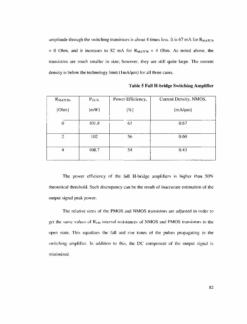
amplitude through the switching transistors is about 4 times less. It is 67 mA for RMATCH
= 0 Ohm, and it increases to 82 mA for RMATCH = 4 Ohm. As noted above, the
transistors are much smaller in size; however, they are still quite large. The current
density is below the technology limit (ImA/fim) for all three cases.
Table 5 Full H-bridge Switching Amplifier
RMATCH, POUT, Power Efficiency, Current Density, NMOS,
|Ohm| fmW] l%] |mA/|im|
0 101.8 61 0.67
2 102 56 0.60
4 108.7 54 0.43
The power efficiency of the full H-bridge amplifiers is higher than 50%
theoretical threshold. Such discrepancy can be the result of inaccurate estimation of the
output signal peak power.
The relative sizes of the PMOS and NMOS transistors are adjusted in order to
get the same values of RON internal resistances of NMOS and PMOS transistors in the
open state. This equalizes the fall and rise times of the pulses propagating in the
switching amplifier. In addition to this, the DC component of the output signal is
minimized.
82
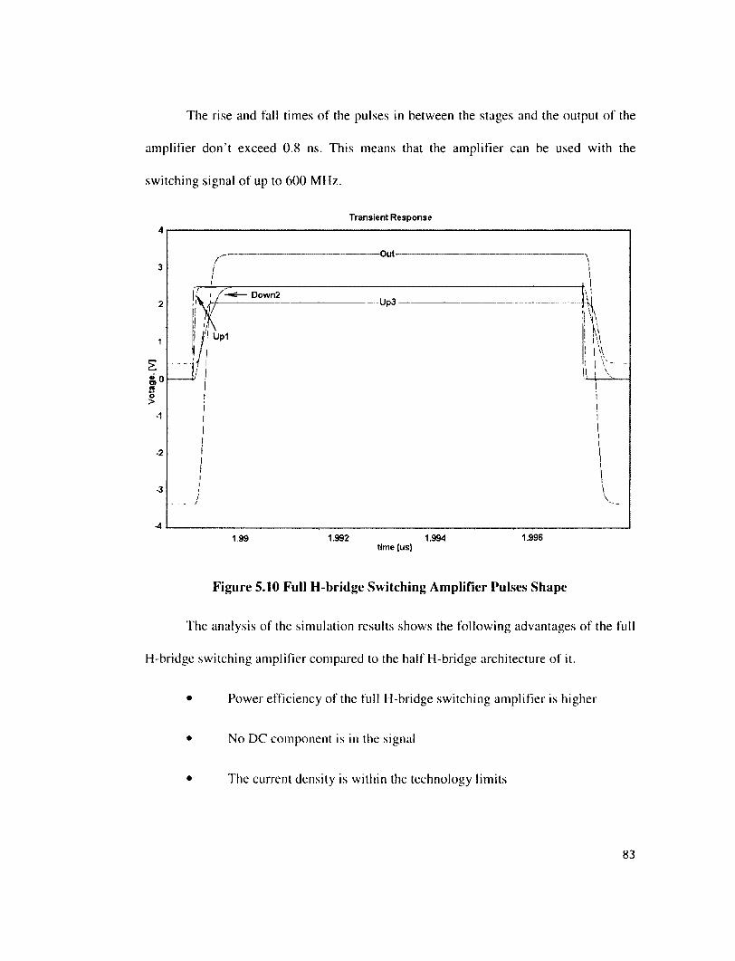
The rise and fall times of the pulses in between the stages and the output of the
amplifier don't exceed 0.8 ns. This means that the amplifier can be used with the
switching signal of up to 600 MHz.
Transient Response
Down2
1 99 1.992 1.994 time (us)
1.996
Figure 5.10 Full H-bridge Switching Amplifier Pulses Shape
The analysis of the simulation results shows the following advantages of the full
H-bridge switching amplifier compared to the half H-bridge architecture of it.
• Power efficiency of the full H-bridge switching amplifier is higher
• No DC component is in the signal
• The current density is within the technology limits
83

• The overall silicon area of the device per output power unit is
significantly smaller
This proves that the full H-bridge switching amplifier is the potential solution
for the ADSL line driver.
5.3 System Verification
5.3.1 Test Benches and Tests Overview
As noted above, the line driver is designed as completely digital device that
consists of two main functional blocks, namely, the 2nd order AI modulator followed by
the switching power amplifier. The AI modulator is built as the set of Verilog modules.
When they are compiled, the Cadence Virtuoso Design Suit creates the schematic
symbols for each Verilog module. This allows incorporating the Verilog modules in the
Virtuoso Schematic Capture tool.
The functionality of the line driver has been comprehensively simulated in
Cadence Analog Design Environment with Spectra and SpectraVerilog simulators.
Appropriate test benches are designed to apply appropriate stimulus signals and to
capture the output signal for further analysis.
The following tests are done to characterize the performance of the ADSL line
driver:
• The evaluation of Dynamic Range of output signal of the line driver;
• The evaluation of Missing Tone Power Ratio at the output of the line
driver.
84
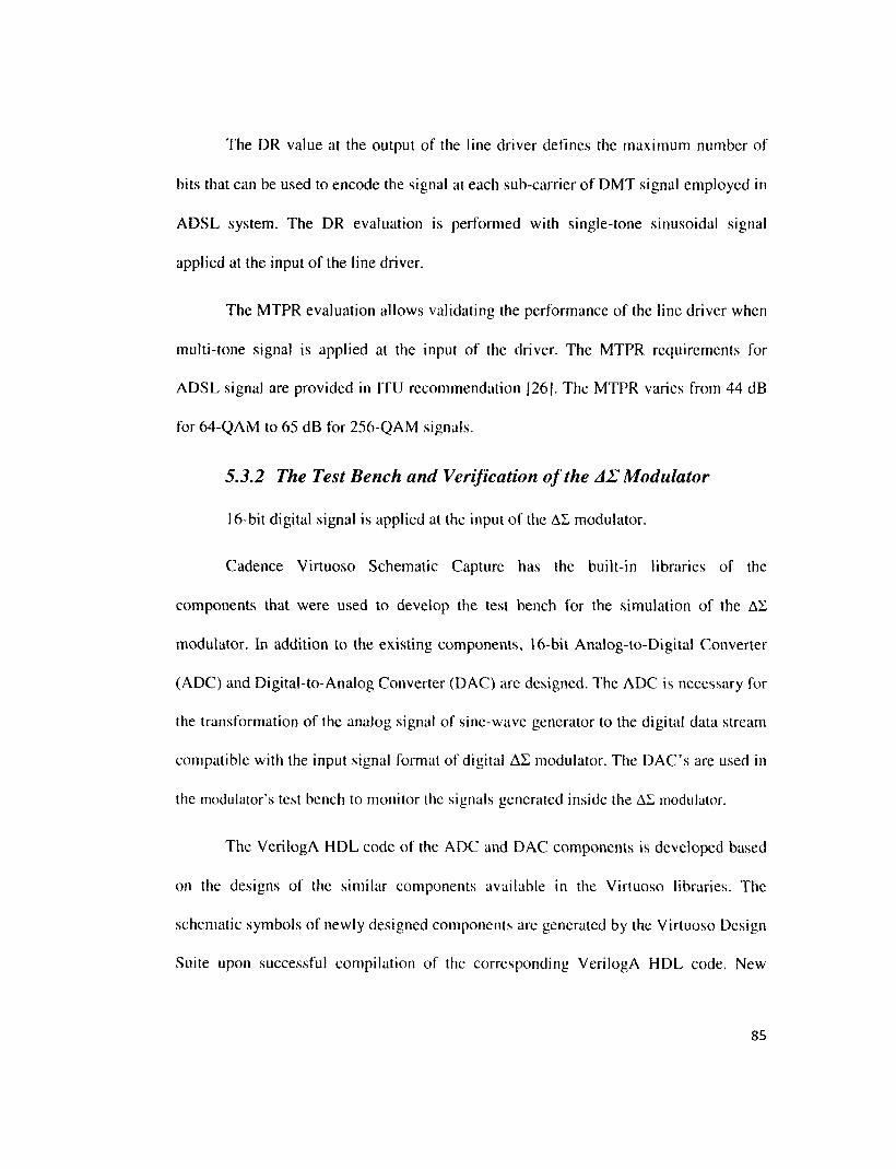
The DR value at the output of the line driver defines the maximum number of
bits that can be used to encode the signal at each sub-carrier of DMT signal employed in
ADSL system. The DR evaluation is performed with single-tone sinusoidal signal
applied at the input of the line driver.
The MTPR evaluation allows validating the performance of the line driver when
multi-tone signal is applied at the input of the driver. The MTPR requirements for
ADSL signal are provided in ITU recommendation [26|. The MTPR varies from 44 dB
for 64-QAM to 65 dB for 256-QAM signals.
5.3.2 The Test Bench and Verification of the AE Modulator
16-bit digital signal is applied at the input of the AX modulator.
Cadence Virtuoso Schematic Capture has the built-in libraries of the
components that were used to develop the test bench for the simulation of the AZ
modulator. In addition to the existing components, 16-bit Analog-to-Digital Converter
(ADC) and Digital-to-Analog Converter (DAC) are designed. The ADC is necessary for
the transformation of the analog signal of sine-wave generator to the digital data stream
compatible with the input signal format of digital AS modulator. The DAC's are used in
the modulator's test bench to monitor the signals generated inside the AL modulator.
The VerilogA HDL code of the ADC and DAC components is developed based
on the designs of the similar components available in the Virtuoso libraries. The
schematic symbols of newly designed components are generated by the Virtuoso Design
Suite upon successful compilation of the corresponding VerilogA HDL code. New
85

ADC and DAC are capable to manage 16-bit digital signals and the analog signals in 0
- 2,5 V amplitude range.
VerilogA code of ADC and DAC components used in the test bench of the line
driver and their associated symbols are provided in Appendix C below.
The test bench for the characterization of the AL modulator is shown in Figure
5.11 below. The AS modulator itself is composed of Adderl, Adder2, Relay and two
Integrator components. The rest components belong to the Test bench. They provide the
input signals to and capture the output signals from the modulator.
The stimulus signal for the SNR and dynamic range measurements is produced
by the sine-wave generator, which analog output is transformed to the 16-bit digital data
stream by the following ADC.
JUL
+^VD * 1 25 V = 130m
freq = 250K
6 V1 = 00 V2 = 25 tr = 10p
vdi
£
JUL
l-
S> V1 =00 V2- 2b
tr = 10p
lnput<15 0>
Sign Output* 1 & 0*
Rst Adderl
lnput<15 0> Sign Output<15 O3
Rsl Adder2
ln<15 0* Out Rst
VDD Rel • VSS Relay notRel —a
lnput< 15 0> Output< 15 0">
Rs1 Integrator
lnput<15 0» Output'15 0^
Rst Integrator
Relay
Figure 5.11 Sigma-Delta Modulator Test Bench
86

Pulse generator f= 128 MHz provides clocking for the AS modulator and acts as
a sample generator for the SNR and DR evaluations. The selection of the clock
frequency is explained in Section 3.3 above.
The schematic includes multiple DAC modules to monitor the signals at the
output of the internal modules. They are helpful in the process of the AS modulator
design and troubleshooting. The screenshots of internal signals are shown in Figure 5.12
below.
Transient ft«*?.pon=p
a) Input Sine-wave Signal
111 i b) Output ot Adder 1
2 3-J
c) Output of Ideal Integartor 1
d) Output of Adder 2
H r o) Output of Integrator 2
fi Hi f) Relay Output
H 1-Tmf.
Figure 5.12 AE Modulator's Internal Signals
87

The output signal of the AL modulator is captured as CSV file and processed
using the Matlab script that is similar to the one used to evaluate the Simulink model of
the modulator.
The script calculates the Power Spectrum Density of the signal and the
histograms of the signal amplitudes at the selected test points of the AS modulator. The
typical example of the histograms at the output of the 1st and 2nd integrators is given in
Figure 5.13 below. The histograms changes from Gaussian-like shape for the "noisy"
analog signal at the input to a sharper shape that corresponds to the signal, which
amplitude becomes close to the voltages of the digital signal domain.
800
700
600
500
400
300
First Integrator Output
100
0!— -1 - 0 5 0 0 . 5
Voltage [VJ
1000
900
800
700
600
500
400
300
200
100
Second Integralor Output
-0.5 0 0 5 1 Voltage [V]
Figure 5.13 Signals Histograms of the A£ Modulator
88

The results of the SNR measurements are given in Figure 5.14 and Figure 5.15
below. The simulation is done for fiN = 250 kHz. The processing bandwidth is BW =
500 kHz.
It is worth to note that the circuitry doesn't include any low-pass filters;
however, no high-order harmonics are observed in the signal at the output of the AE
modulator. As per the definition of the Dynamic Range done in Section 3.3 the DR of
the AL modulator in Figure 5.11 is at least 85.8 dB.
o
-20
-40
-60
CD T3 o i f ) a
- ! 00
CO
- '40
- : I-.I I 0 0 .2 0 4 0 0 3 8 • 1.2 I 4 10 'ft 2
Frequency [Hz] x ]0?
Figure 5.14 Signal Spectrum of 2nd-order Modulator, = 250 kHz, BW = 500 kHz
•SNR = OfeR= 128
iRbit ~ 13.05 bits @ DSR-12&
89
KO
o -100
120
Frequency [Hz]
Figure 5.15 Signal Spectrum of 2nd-order AL Modulator, fiN = 250 kHz, BW = 500 kHz
The MTPR evaluation is done with vpwlf component as the signal source instead
of the sine-wave generator. The vpwlf component includes the ascii file with the record
of the signal that is generated by Simulink during the simulation of the ADSL
modulator model |6|. The recorded signal represents the instantiation of the 256-QAM
DMT signal, but with few sub-channels been switched off. The appearance of the signal
at the input of the AS modulator is shown in Figure 5.16 below.
The frequency of the clock generator is changed to f= 131.072 MHz for the
MTPR evaluation. The frequency is the multiple of sample frequency of the incoming
signal fs = 4000 Hz, number of channels/tones NTONE = 256 and the buffer size NBUF =
90

128. The buffering makes frame-based signal format that is required for the FFT
algorithm to compute the signal PSD.
2.25
2.0
1.75
S16 ' • CD IB
O > 26
1.0
.75
.5 0 100 200 300 400 600 600
Time. Fusl
Figure 5.16 DMT Signal Instantiation at the A£ Modulator's Input
The signals at the output of the AE modulator are saved in an ascii file. The
OCEAN script below is used to capture the signal in the file.
ocnPrint(VT("/Out") ?output "/home/starych/thesis/SigmaDelta/File"
?numberNotation 'none ?precision 14)
Such way of data capture improves the resolution of the data to be processed and
so minimizes the signal distortion at the input of the processing jig.
The MTPR value is estimated as the drop of signal power density at the
frequencies of missing sub-channels. The bottom level of the power density within the
91
Transient Response

drop represents the intrinsic noise of the AL modulator and inter-modulation products
generated when the DMT signal is applied.
The Simulink toolbox for the MTPR evaluation is shown in Figure 5.17 below.
Sept05_Rel_SDM_SwAmp3 5th-order
LPF
i 5th-order
LPF j*stj
From Workspacel
' 64
Digital Filter Buffer
Downsample FFT
Transmit Spectrum
Figure 5.17 ADSL Signal Processor for MTPR Evaluation
The digital low-pass filter of BW = I MHz bandwidth is placed in front of the
processor. This filter is not the part of the line driver and is intended to filter out high-
frequency noise during the signal processing.
-10
-201-
-30
-40 CD ID 6 -50 ID i i c -60 il C7> 1 TO
-70 r
1 C
O
o
-90
1 o
o
S>l < j I f f s
0 0.:
Frame: 3
J ' * r- \
t; V
0.4 0.6 Frequency (MHz)
Figure 5.18 MTPR of 2nd-order A£ Modulator
92

The result of the AS modulator circuit simulation is shown in Figure 5.18 above.
The MTPR at the output of the modulator designed for this work is about 70 dB. This
value is 5 dB better compared to the corresponding Simulink model of the AZ
modulator (see Figure 3.19 in Chapter 3 above).
5.3.3 Line Driver Characterization
The line driver is composed of the AS modulator followed by the power
amplifier. The evaluation of SNR, DR and MTPR parameters are done for the whole
circuit. Such approach allows estimating the saturation of the line driver's performance
due to the switching power amplifier, if necessary, because the performance of the AZ
modulator itself was evaluated earlier. The schematic of the line driver is shown in
Figure 5.19 below.
The schematic includes the components that belong to the test bench of the line
driver. The components shown in Figure 5.19 (the sine-wave generator, the reset-pulse
generator and the clock generator) are used to simulate the operation of the line driver
for the evaluation of its SNR and DR. The frequency of the clock generator is f = 128
MHz.
The results of the SNR evaluation for the signal of frequency 1'IN = 250 kHz and
peak power P = 100 mW at the output of the line driver are provided in Figure 5.20 and
Figure 5.21 below.
93

Input V3
freq = 250K
JUL
V1 = 0 0 JUL
If = 10p
gnd
Rel M3
*pch'
OOn 1=160 OOn
Out Upl Up2 Up3
"nch"
1=180 OOn W=1 3u
I.OOn 1=180 OOn
R3
M7
"pch"
1 M9
"pch"
1 M11
"pch"
1=180 OOn w=39u
Downl Down 2 notRel
M10 M12
gnd OOn 1=180 OOn
ADC_16b
lnput<15.0> Sign
lnpul<15 0>
Integrator
Integrator
Output<15 0>
lnput<15:0>
Sign
Rst
VDD
Relay
Rel
Figure 5.19 ADSL Line Driver Schematic
94

0
-20
-40
-00
ET T>
Q "80 w a
-100
- 1 2 0
- uo
- ir.o 0 0.2 0 4 0 6 O.ii I 1.2 14 i 0 i 8 2
Fluency [Hz] x ,fi-i
Figure 5.20 Signal Spectrum of the Line Driver with Switching Power Amplifier, f,N = 250 kHz, BW = 500 kHz
The analysis of the signal's spectrum shows that the level of unwanted
harmonics at the output of the line driver is extremely low. The 3 lcJ harmonic at f = 750
kHz frequency is observed only. The level of the harmonic is 80 dB below the PSD
level at the signal's main frequency. It is worth to note that no filters are used in the line
driver at all.
The Spurious Free Dynamic Range (SFDR) of the signal at the output of the line
driver can be estimated as 80 dB in 1 MHz bandwidth and about 70 dB in 2 MHz
bandwidth.
95

#
10 ' 10 '
Frequency [Hz]
Figure 5.21 Signal Spectrum of the Line Driver with Switching Power Amplifier, f,N = 250 kHz, BW = 500 kHz
The simulation results in Figure 5.20 and Figure 5.21 are for the switching
power amplifier with RMATCH = R1 = R2 = 2 Ohm resistor. As one can see, the SNR
value is 2.5 dB smaller at the output of the switching power amplifier compared to the
signal SNR at the input of the amplifier (see Figure 5.14 above).
The SNR value for the circuit with RMATCH = 0 Ohm is the same. The main
difference between the circuits with different RMATCH values is the current density in the
switching transistors of the amplifier, J = 0.67 mA/fim and J = 0.60 mA/|im accordingly
as per Table 5 above. This confirms that the current density is not critically high, and
96

the unwanted processes like hot-carrier generation that are often associated with high
current density, don't contribute into the circuit noise.
The dynamic range of the line driver in Figure 5.19 above is additionally
evaluated for the range of signals at the driver's input to make sure that the SNR value
depicted in Figure 5.20 is the maximum and provides the correct DR estimation of the
line driver. The results are shown in Figure 5.22 below. The circuit demonstrates the
dynamic range DR = 83 dB, which is about 10 dB less than SNDR = 94 dB calculated
in Section 3.3 for the 2nd-order AL modulator.
10 30 60 100
Input Signal, mV
Figure 5.22 Dynamic Range of the Line Driver, f|N = 250 kHz, BW = 500 kHz
The SNR value in dB is directly related to the number of bits of the digital signal
that is applied to modulate each carrier in the DMT signal:
SNR-1.76 R= 6.02 (5-2 '
Accordingly, the dynamic range can be plotted as shown in Figure 5.23 below.
97
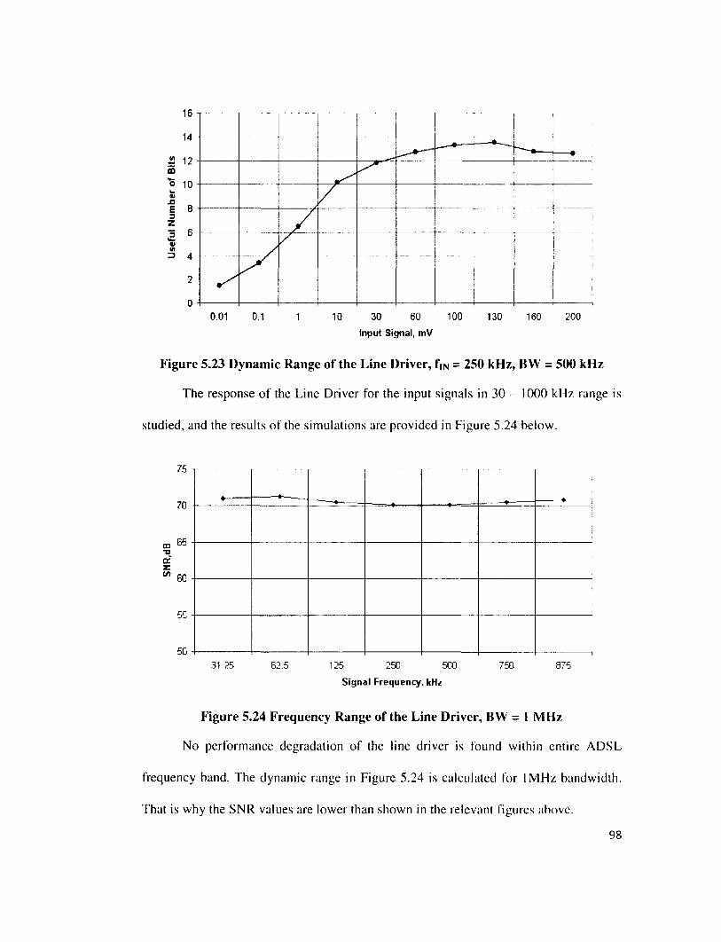
16 -
14
s
L_ a> •i n t o 3 Z 3 b u— 0) v> => 4
2
0
-— — • - - — — -
0.01 0 1 1 10 30 60 100 130 160 200
Input Signal, mV
Figure 5.23 Dynamic Range of the Line Driver, f(N = 250 kHz, BW = 500 kHz
The response of the Line Driver for the input signals in 30 - 1000 kHz range is
studied, and the results of the simulations are provided in Figure 5.24 below.
7 5 - , -
D 65 : T3 G:
"> Q]
55
50 \ , 31 25 62.5 125 250 500 750 875
Signal Frequency, kHz
Figure 5.24 Frequency Range of the Line Driver, BW = 1 MHz
No performance degradation of the line driver is found within entire ADSL
frequency band. The dynamic range in Figure 5.24 is calculated for 1MHz bandwidth.
That is why the SNR values are lower than shown in the relevant figures above.
98

The MTPR characterization of the line driver is done with the same test bench as
used for the dynamic range study, but with the sine-wave generator replaced for the
vpwlf component described in Section 5.3.2.
The frequency of the clock generator is changed to f= 131.072 MHz for the
MTPR evaluation. The frequency is the multiple of sample frequency of the incoming
signal fs = 4000 Hz, number of channels/tones NTONF. = 256 and the buffer size NNUI- =
128. The buffering makes frame-based signal format that is required for the FFT
algorithm to compute the signal PSD.
The signal at the output of the line driver is captured using the Ocean script and
processed with the Simulink toolbox as explained in Section 5.3.2.
As reported in Section 5.3.2 the MTPR is 70 dB at the output of the AL
modulator of 2nd order (Figure 5.18 above). The same value MTPR = 70 dB for BW =
1MHz is found for the signal at the output of the switching power amplifier (Figure 5.25
below).
The Line Drivers with RMATCH = 0 Ohms and RMATCH = 2 Ohms are simulated
for the MTPR evaluations. Both drivers exhibit the same performance. The switching
amplifier itself doesn't degrade the MTPR. This result is somewhat expected as the
amplifier is not supposed to change the shape of the signal, and so it doesn't disturb the
spectrum of the signal.
99

-10
-20
-30
-40 CD "O
a> -50 x> 3
c -60 CD 03
5 -70
-80
-90
-100
l" r, r
». I A,|VV| : I A, }\ * ii i \ r, i i i» i ,wvv t
f •• X- - m
<| w ! !i !i
0 0.2
Frame: 3
^Vvv*-k. i I ij U •',% I ' 1 A
"/'W
0.4 0.6 Frequency (MHz)
* r\, 1/ -A
Lj u-l
0.8
Figure 5.25 MTPR of the ADSL Line Driver
100

6 Conclusions and Future Work
6.1 Summary
The system solution for ADSL line driver is studied. The proposed line driver is
composed of the AS modulator followed by the switching power amplifier. The
modulator is implemented as the digital circuit that transforms multi-bit code generated
by IFFT DSP into single-bit digital signal. The latter one is amplified by the switching
power amplifier and routed into ADSL communication link.
Simulations showed that 2nd-order low-pass AS modulator is capable to produce
the signal suitable for ADSL applications. Simulink model of the modulator exhibits the
DR = 85 dB for fiN— 250 kHz signal in BW = 500 kHz bandwidth. The clock frequency
is approximately 130 MHz. The frequency is feasible for 0.18 fim CMOS technology
that is preliminarily selected for the silicon implementation of the line driver.
The Simulink model of 2nd-order AS modulator provides suitable performance
when DMT signal is applied at its input. The MTPR value is approximately 70 dB that
is 5 dB higher than the maximum MTPR expected when 256-QAM DMT signal is
employed.
The modules of AS modulator are designed in Verilog HDL and compiled. The
corresponding components are simulated in Cadence Virtuoso Design Environment
together with switching power amplifier. The switching amplifier is composed of three
CMOS invertors connected in series. The transistors of the last switching stage are
made large enough to provide the signal of P|. = 100 mW power in R|. = 100 Ohm load.
101

The matching circuitry is included in the switching amplifier to improve the efficiency
of the transmission chain. The power efficiency of the switching power amplifier is
approximately 60% as per simulation results.
The simulations show that the line driver can provide the DR = 83 dB in BW =
500 kHz bandwidth for the signals in 30 - 1000 kHz frequency range. The MTPR value
is 70 dB in BW = 1 MHz bandwidth.
Spurious Free Dynamic Range SFDR = 80 dB in BW = 1 MHz and SFDR = 70
db in 2 MHz bandwidth. The only spurious signal observed in BW = 2 MHz is the 3rd
harmonic of the main signal. The level of the harmonic is 80 dB less than the level of
the signal main harmonic.
The proposed solution for the ADSL line driver seems very promising. Being
completely digital, it allows using standard CMOS technology for the circuit
fabrication. The AS modulator doesn't include any analog modules that are usually
associated with complicated calibration techniques and circuit trimming.
6.2 Results Comparison
The AS modulator as a data formatter and switching power amplifier are not
usually studied together as the solution for the ADSL line driver. This is one of the
reasons why the number of relevant technical publications is very low. That is why the
publications that are referred below are sorted out for two groups. The first group
includes the technical papers that study the AS modulators, which are close to the one
presented in this work from view point of architecture or application. The second group
includes the publications that discuss high-efficient line drivers/transmitters that can be
102

used for ADSL communication links regardless of their circuitry solutions and the data
formatters preceding the amplification stages.
Most AS modulators, which are discussed in professional technical publications,
are designed as analog circuits. The authors are forced to use high-order architectures of
the modulators to get the required specifications (dynamic range and SNR). As the AE
modulators of the order of three and higher are conditionally stable and require special
means to prevent oscillations, so-called Multi-stage Noise Shaping (MASH) topologies
are often used. MASH AS modulators are the modulators of Is ' and 2nd- order connected
in series. 2-1-1 topology is very popular solution as it provides necessary performance
while being unconditionally stable and relatively simple in its implementations. Almost
all AX modulators listed in Table 6 below are designed as MASH devices.
The modulators in the table are analog circuits. The integrators are designed
based switched-capacitor technique. Although the modulators are built as CMOS
devices, extra technology extensions are usually used to implement the circuit elements,
for example, Metal-Insulator-Metal fabrication process to build the capacitors.
Trimming is usually required to fabricate the circuit components with necessary
accuracy.
The integrator designed for this work is pure digital circuit that can be fabricated
with generic CMOS process without any technology extensions that might be required
for the implementation of analog components. The circuit is not locked to some
particular CMOS technology. The only limitation is the signal delay. It is determined
above that 0.18|jm CMOS seems to be suitable for the AS modulator studied in this
103

work. More advanced technology, for example, 90 nm CMOS can be used as well as it
provides less signal delays. Required performance is gotten with low-order modulator
topology due to high sampling frequency and, accordingly, high OSR. The circuit
performance is tailored for ADSL application only. That is why the circuit study is done
for the signal frequency range up to 1 MHz only.
Table 6 Modulators
Reference Topology
Power
Supply,
IV]
OSR
Sample
Frequency,
|MHzl
DR,
IdB] Note
[15! 2-1-1 3.3 24 52.8 87
0.5pm CMOS,
analog SC
integrators
[161 2-1-1 2.5 32 70.4 85
0.25pm CMOS,
MTPR-81 dB,
BW = 2.2 MHz
[17| 2-1-1 1.8 24 50 70
0.18pm CMOS,
analog SC
integrators
1181 4 1.8 10 200 82
0.18pm CMOS,
analog SC
integrators,
BW = 10 MHz
This work 2 2.5 128 128 83 0.18pm CMOS,
digital circuit
The &L modulator designed for this work demonstrates satisfactory performance
while being robust and having simple topology. This becomes possible due to high
speed of digital circuits that is one of the advantages of modern CMOS technologies.
104
It should be noted that the top performance of the AZ modulator is not the main
goal of the design. The proposed modulator is expected to meet the ADSL
specifications with some margin in order to be used as the data formatter for the
following power amplifier. The power efficiency of the amplifier, which is used as the
output stage of the ADSL line driver, is considered as more important figure of merit of
the device designed for this work.
The switching power amplifier, which is very natural solution for the CMOS
technologies, is proved to be one of the most power-efficient circuits for DSL links.
Almost all the references provided in Table 7 below, study the implementations of the
switching amplifier, which output stage is made as standard PMOS-NMOS stacked
transistor pair. With regards to the switching power amplifiers, this circuit is often
referred as half H-bridge topology.
Although the circuitry made of NMOS-PMOS transistor pole seems simple, the
designers propose different implementations of it to address the technology and
application related restrictions.
SOPA concept proposed in |3) is one of the first attempts to resolve the problem
of low power-efficiency of Class AB power amplifiers for high CF DSL signals. It is
remarkable that the authors decided to look for the solution within CMOS framework.
The SOPA topology proposed as the data formatter allows using switching power
amplifier at the output of the circuit. The resultant circuit outperforms the analog power
amplifiers and meets ADSL and VDSL requirements.
105
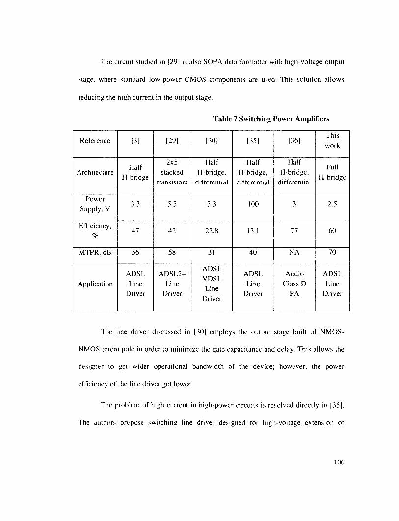
The circuit studied in [29] is also SOPA data formatter with high-voltage output
stage, where standard low-power CMOS components are used. This solution allows
reducing the high current in the output stage.
Table 7 Switching Power Amplifiers
Reference [3] [29] [30] 135] [36] This
work
Architecture Half
H-bridge
2x5
stacked
transistors
Half
H-bridge,
differential
Half
H-bridge,
differential
Half
H-bridge,
differential
Full
H-bridge
Power
Supply, V 3.3 5.5 3.3 100 3 2.5
Efficiency,
% 47 42 22.8 13.1 77 60
MTPR, dB 56 58 31 40 NA 70
Application
ADSL
Line
Driver
ADSL2+
Line
Driver
ADSL
VDSL
Line
Driver
ADSL
Line
Driver
Audio
Class D
PA
ADSL
Line
Driver
The line driver discussed in [30| employs the output stage built of NMOS-
NMOS totem pole in order to minimize the gate capacitance and delay. This allows the
designer to get wider operational bandwidth of the device; however, the power
efficiency of the line driver got lower.
The problem of high current in high-power circuits is resolved directly in 135].
The authors propose switching line driver designed for high-voltage extension of
106

standard 0.7 pm CMOS technology. The power efficiency of the circuit is increased
compared to Class AB power amplifiers, but it is still lower than reported in [3).
The AS modulator is proposed as the data formatter of the line driver for audio
signal in |36|. The output stage of the line driver is designed as the switching power
amplifier. The 4th-order AS modulator uses SC analog integrators with high switching
frequency.
The devices referred in Table 7 above are designed for different technical
specifications, and so it is not quite fair to compare their performance relative to each
other. However, the references give the overall impression about the progress in the
design of power-effective DSL line drivers.
6.3 Thesis Contribution
The main goal of this work is to build high efficient ADSL line driver driven by
digital data encoder. As the result, the circuit composed of AS modulator followed by
switching power amplifier is proposed.
Such system solution has been discussed in technical community. However, it is
not considered as the real opportunity for xDSL applications. That is why probably no
publications, which would discuss this solution in professional manner, are found in
technical literature.
It should be noted that the AS modulator is very popular circuit. It is usually
used in Analog-to-Digital Converters. The AS modulator as part of ADC module is
often built as an analog device, mostly based on switched-capacitor integrators. No pure
107

digital implementation of the AE modulator or HDL code of the AL modulator of 2nd-
order and higher are found in the technical literature at all.
The contributions of the thesis work can be defined as follows.
• The system solution for the ADSL digital line driver, which is composed of
the AS modulator and switching amplifier, is justified.
• The architecture of the AS modulator is defined by thorough simulations of
Simulink model of the modulator.
• The Verilog code of the AZ modulator is written, compiled and integrated in
Cadence Virtuoso Design Environment..
• The application of switching power amplifier for ADSL signal is justified.
• The test bed for ADSL signal is designed.
• High DR and MTPR values have been demonstrated.
• The power efficiency of the switching line driver is estimated. It is found
that the efficiency is close to the theoretical level of 50%.
• The proposed line driver demonstrates very low level of unwanted
harmonics in the output signal spectrum. The result is gotten without using
any filters at the output of the driver.
It is expected that the proposed solution is applicable not only to DMT-based
ADSL links, but also can be used in any other Ultra-Wide Band (UWB) communication
systems that employ OFDM technology.
108
6.4 Recommendations and Future Work
The current work should be considered as comprehensive, but still paper study
of the ADSL line drivers. Proposed system solution is very promising; however, its
feasibility can be Finally judged only based on the test results of the real device. The
implementation of the proposed line driver on the silicon is the very first thing to do.
It is probably useful to make the AX modulator design, as the first approach, in
an FPGA prototype. The FPGA is quite powerful and flexible platform that allows the
designer to catch the weak sides of the design at its early stage. When the design of the
AE modulator is proved, the circuit can be fabricated as an ASIC, if necessary.
VLSI circuits when fabricated have very limited possibilities with regards to the
changes of the circuits that might be found necessary during the circuit troubleshooting
and evaluation. That is why the thorough verification and post-layout simulation of the
synthesized circuit should be completed.
Post-layout simulation is very important for the design of the AE modulator and,
in particular, for the switching power amplifier. The large size of the amplifier's
switching transistors is associated with large parasitic capacitances that spread over the
circuitry. They can significantly affect the performance of the amplifier. However, the
successful designs of high-power switching amplifiers are reported in many
publications. This proves that the problem of the parasitic capacitances can be resolved.
The other challenge associated with the design of the switching power amplifier
is high current density. It could reduce the reliability of the circuit if the conductors are
not made wide enough. Also too high currents can generate extra noise in the circuitry.
109
This factor is essential for the receivers, and so it is better to keep it in mind as well
when the line driver is being designed.
2nd-order AS modulator has been studied in this work. It provides suitable
performance the ADSL communication links. The other topologies of the modulator can
be studied in order to determine if they provide better performance. The AS modulator
architecture suitable for VDSL standard can be defined as well.
110

7 References
f 1 ] Jan Sevenhans et al., "Driving the DSL Highway: high speed, high density,
low power, low cost", Proceedings of the 28th European Solid-State
Conference, ESSCIRC, pp.555-562, 2002.
12] S.-S. Le, "Integration and System Design Trends of ADSL Analog Front
Ends and Hybrid Line Interfaces", Proceedings of the IEEE Custom
Integrated Circuits Conference, pp.37-44, 2002.
[3] T. Piessens, M.Steyaert, "Highly Efficient xDSL Line Drivers in 0.35-um
CMOS Using a Self-Oscillating Power Amplifier", IEEE Journal of Solid-
State Circuits, Vol. 38, No. 1, pp.22-29, 2003.
1.4] S. Saponara, L. Serafini, L. Fanucci, "Low-power FFT/IFFT VLSI Macro
Cell for Scalable VDSL Modem", Proceedings of 3rd IEEE International
Workshop on SoC for Real-Time Applications, 2003.
[5| M. Nava, C. Del-Toso, "A Short Overview of the VDSL System
Requirements", IEEE Communication Magazine, Vol.40, pp.82-90, 2002.
|6] O.W. Ibraheem, N.N. Khamiss, "Design and Simulation of Assymmetric
Digital Subscriber Line (ADSL) Modem", 3rd International Conference on
Information and Communication Technologies: from Theory to
Applications, pp. 1-6, 2008.
Ill

[71 Asymmetric Digital Subscriber Line (ADSL) Transceivers, ITU-T
Recommendation G.992.I, 1999.
[8] Splitterless Asymmetric Digital Subscriber Line (ADSL) Transceivers, ITU-
T Recommendation G.992.2, 1999.
[9] M. Debbah, "Short Introduction in OFDM", Alcatel-Lucent, White paper.
[10] J.Candy, "The Structure of Quantization Noise from Delta-Sigma
Modulators", IEEE Transactions on Communications, Vol. 29, No.9, 1989.
[11| N. Maghari, S. Kwon, G. C. Temes, U. Moon, "Sturdy MASH A-S
Modulator", Electronics Letters, October 2006, Vol. 42, No.22.
[12| S. Brigati, F. Francescony, P.Malcovati, F.Maloberti, "Modeling Band
pass Sigma-Delta Modulators in Simulink" Proceedings of International
Workshop on ADC Modeling and Testing, IWADC 2000, Vienna, Austria,
September 2000.
[13] C.-I. Lao, H.-I. Ieong, K.-F. Au, K.-H. Mok, S.-P. U, R. Martins, "A 10.7
MHz Bandpass Sigma-Delta Modulator Using Double Delay Single-opamp
SC Resonator with Double-Sampling", Proceedings of International
Symposium on Circuits and Systems ISCAS'03, IEEE, Vol. I, pp. 1061-
1064, 2003.
[ 14) J. M. de la Rosa, B. Perez-Verdu, F. Medeiro, A. Rodriguez-Vazquez "A
2.5 MHz 55dB Switched-Current Bandpass Delta-Sigma Modulator for AM
112

Signal Conversion", Proceedings of European Solid-State Circuits
Conference, pp. 156-159, 1997.
[ 15J Y. Geerts, A. Marques, M. Steyaert, W. Sansen, "A 3.3-V, 15-bit, Delta-
Sigma ADC with Signal Bandwidth of 1.1 MHz for ADSL Applications",
IEEE Journal of Solid-State Circuits, Vol.34, No.7, July 1999.
116J R. del Rio, J. M. de la Rosa, B. Perez-Verdu, M. Delgado-Restituto, R.
Dominguez-Castro, F. Medeiro, A. Rodriguez-Vazquez "Highly Linear 2.5-
V CMOS Delta-Sigma Modulator for ADSL+", IEEE Transactions on
Circuits and Systems I: Regular Papers, Vol. 51, pp.47-62, 2004.
[17] M. Safi-Harb, G. W. Roberts "Low-Power Delta-Sigma Modulator for
ADSL Applications in Low-Voltage CMOS Technology", IEEE
Transactions on Circuits and Systems I: Regular Papers, Vol. 52, pp.2075-
2089, 2005.
118] P. Balmelli, Q. Huang "A 25-MS/s 14-b 200-mW £A Modulator in 0.18-
|jm CMOS". IEEE Journal of Solid-State Circuits, Vol. 39, No. 12, 2004.
[ 19] J. B. Hughes, I. C. Macbeth, D. M. Pattullo "Second Generation Switched-
Current Signal Processing", IEEE International Symposium on Circuits and
Systems, Vol. 4, pp.2805-2808, 1990.
[20) J. B. Hughes, K. W. Moulding "Switched-Current Signal Processing for
Video Frequencies and Beyond", IEEE Journal of Solid-State Circuits,
Vol.28, No.3, March 1993.
113

[21] N. Tan, S. Eriksson "A Low-Voltage Switched-Current Delta-Sigma
Modulator", IEEE Journal of Solid-State Circuits, Vol. 30, No. 5, 1995.
[22] N. Khitouni, S. Boujelben, M. Masmoudi "Switched Current Integrator for
Second Order Sigma Delta Modulator", The 16th International Conference
on Microelectronics, ICM 2004 Proceedings, pp.595-599, 2004.
[23] S. Masmoudi, M. Fakhfakh, M. Loulou, N. Masmoudi, L. Loumeau "A
CMOS 80 MHz Low-pass Switched-Current Fourth Order Sigma Delta
Modulator", IEEE International Conference on Sensors, Circuits and
Instrumentation Systems, Hammamet, Tunisia, 2007.
[24] N. Moeneclaey, A. Kaiser "Design Techniques for High-Resolution
Current-Mode Sigma-Delta Modulators, IEEE Journal of Solid-State
Circuits", Vol. 32, No. 7, 1997.
[25] J. Hughes, A. Worapishet, C. Toumazou "Switched-Capacitors versus
Switched-Current: a Theoretical Comparison", The 2000 IEEE International
Symposium on Circuits and Systems, ISC AS, Proceedings, Vol. 2, pp.409-
412, 2000.
[26] Asymmetric Digital Subscriber Line Transceivers 2 (ADSL2), ITU-T
Recommendation G.992.3, 2002.
[27] S. Brigati. F. Francesconi, P. Malcovati, D. Tonietto, A. Baschirotto, F.
Maloberti, "Modeling Sigma-Delta Modulator Non-Idealities in Simulink",
Proceedings of the 19lh International Symposium on Circuits and Systems,
ISCAS'99, Vol.2, pp.384-387, 1999.
114
(281 S. R. Norsworthy, R. Schreier, G. C. Temes, Delta-Sigma Data Converters,
Theory, Design and Simulation, New York: IEEE Press, 1997.
[29] B. Serneels, M.Steyaert, W. Dehaene, "A 237mW aDSL+ CO Line Driver
in Standard 1.2V 0.13pm CMOS", Digest of Technical Papers, IEEE
International Solid-State Circuits Conference, ISSCC 2007, pp.524-619,
2007.
[30] S. Maugham, R. Henderson, "A Wide Band CMOS Class-D Line Driver
for Wireline Communication", 53rd IEEE International Midwest Symposium
on Circuits and Systems (MWSCAS), pp.769-772, 2010.
[311 0.18 nm CMOS Process (CS80A),
http://www.fuiitsu.com/downloads/MICRQ/fma/pdf/csm80a.pdf.
[32J Products: ASIC (Gate Arrays),
http://www.epson.ip/device/semicon e/product/asic/gatearray.
[33] M. M. Mano, C. R. Kime, "Logic and Computer Design Fundamentals",
4th Edition, Pearson Prentice Hall, 2008.
|34] TSMS 0.18 jim Logic 1P6M Salicide 1.8V/3.3V Design Rule, Doc. No.
TA-I0A5-4001 (T-018-LO-DR-OO1), Rev.2.2.
[35[ V. de Gizelle, J. Doutreloigne, A. van Calster, "A High-Voltage, 75mW
Switching ADSL Line-Driver", The 17lh International Conference on
Microelectronics, ICM 2005, p.5, 2005.
115

[36) K. Kang, J. Ron, Y. Choi, H. Nam, S. Lee, "Class-D Audio Amplifier
Using 1-Bit Forth-Order Delta-Sigma Modulation", IEEE Transactions on
Circuits and Systems - II: Express Briefs, Vol. 55, No. 8, 2008.
116

Appendix A - Matlab Processing Toolbox
The original files can be found in
http://www.mathworks.com/matlabcentral/fileexchange/25811 -sdtoolbox-2.
The lines of the files modified for the purpose of this work are noted as adjusted
for ADSL case.
A.l SDM Main Processor
o/ ************************************************************************ /o
% This file processes the results of simulation of 2nd Order Sigma-Delta
% Modulator (SDM Thesis.mdl).
% 1. Plots the Power Spectral Density of the bit-stream
% 2. Calculates the SNR
% 3. Calculates histograms at the integrator outputs
O/ ************************************************************************ /O
clear
tO=clock;
bw=500000; % Bandwidth, adjusted for ADSL case
R=128; % OSR, adjusted for ADSL case
Fs=2*R*bw; % Sampling frequency
Ts=1/Fs;
N=65536; % Samples number
L=N;
nper=128; % adjusted for ADSL case
Fin=nper*Fs/N; %lnput signal frequency
Ampl=0.159; %lnput signal amplitude, adjusted for ADSL case
Ntransient=0
% Modulator coefficients
117

echo on;
b1 =0.5; % adjusted for ADSL case
b2=0.5; % adjusted for ADSL case
Vref=0.5; % adjusted for ADSL case
Amax=0.75; % Op-amp saturation value [V], adjusted for ADSL case
echo off;
finrad=Fin*2*pi; % Input signal frequency in radians
sO=sprintf( ** Simulation Parameters **')
s1=sprintf( Fs(Hz)=%1.0f',Fs);
s2=sprintf( Ts(s)=%1.6e',Ts);
s3=sprintf( Fin(Hz)=%1.4f',Fin);
s4=sprintf( BW(Hz)=%1.0f',bw);
s5=sprintf( OSR=%1.0f,R);
s6=sprintf( Npoints=%1.0f',N);
s7=sprintf( tsim(sec)=%1.3f',N/Fs);
s8=sprintf( Nperiods=%1.3f,N*Fin/Fs)
disp(sO)
disp(s1)
disp(s2)
disp(s3)
disp(s4)
disp(s5)
disp(s6)
disp(s7)
disp(s8)
/O
% Open Simulink diagram first
118

/o
options=simset('lnitialState', zeros(1,2), 'RelTol', 1e-3, 'MaxStep', 1/Fs);
sim('SDM_Thesis', (N+Ntransient)/Fs, options); % Starts Simulink
simulation
/o
% Calculates SNR and PSD of the bit-stream and of the signal
O/ ***•***•********•*****************************'*•***#**•*****************• /O
w=hannSDT(N);
echo on;
f=Fin/Fs % Normalized signal frequency
fB=N*(bw/Fs) % Base-band frequency bins
yy1=zeros(1 ,N);
yy1 =yout(2+Ntransient:1 +N+Ntransient)';
echo off;
ptot=zeros(1,N);
[snr,ptot]=calcSNR(yy1 (1 :N),f,fB,w,N,Vref);
Rbit=(snr-1,76)/6.02; % Equivalent resolution in bits
0/ ************************************************************************** /o
% Output
/o
figure(1);
elf;
plot(linspace(0,Fs/2,N/2), ptot(1:N/2), 'r');
grid on;
title('PSD of a 2nd-0rder Sigma-Delta Modulator')
xlabel('Frequency [Hz]')
ylabel('PSD [dB] )
axis([0 Fs/2 -220 0]);
119
figure(2);
elf;
semilogx(linspace(0,Fs/2,N/2), ptot(1:N/2), 'r');
grid on;
title('PSD of a 2nd-Order Sigma-Delta Modulator')
xlabel('Frequency [Hz]')
ylabel('PSD [dB]')
axis([0 Fs/2 -220 0]);
figure(3);
elf;
plot(linspace(0,Fs/2,N/2), ptot(1:N/2), 'r');
hold on;
title('PSD of a 2nd-Order Sigma-Delta Modulator (detail)')
xlabel('Frequency [Hz]')
ylabel('PSD [dB]')
axis([0 2*(Fs/R) -220 0]);
grid on;
hold off;
text_handle = text(floor(Fs/R),-40, sprintf('SNR = %4.1fdB @
OSR=%d\n',snr,R));
text_handle = text(floor(Fs/R),-60, sprintf('Rbit = %2.2f bits @
OSR=%d\n',Rbit,R));
s1 =sprintf(' SNR(dB)=%1,3f',snr);
s2=sprintf(" Simulation time =%1.3f min',etime(clock,t0)/60);
disp(s1)
disp(s2)
/o
% Histograms of the integrator outputs
120
o / * * * * * * * * * * * * * * * * * * * * * * * * * * * * * * * * * * * * * * * * * * * * * * * * * * * * * * * * * * * * * * * * * * * * * * * * /o
figure(4)
nbins=200;
[bin1,xx1]=histo(y1, nbins);
[bin2,xx2]=histo(y2, nbins);
elf;
subplot(1,2,1), plot(xx1, bin1)
grid on;
title('First Integrator Output')
xlabel('Voltage [V]')
ylabel('Occurrences')
subplot(1,2,2), plot(xx2, bin2)
grid on;
title('Second Integrator Output')
xlabel('Voltage [V]')
ylabel('Occurrences')
A2 calcSNR
function [snrdB,ptotdB,psigdB,pnoisedB] = calcSNR(vout,f,fB,w,N,Vref)
% SNR calculation in the time domain (P. Malcovati, S. Brigati)
% vout: Sigma-Delta bit-stream taken at the modulator output
% f: Normalized signal frequency (fs -> 1)
% fB: Base-band frequency bins
% w: windowing vector
% N: samples number
% Vref: feedback reference voltage
%
% snrdB: SNR in dB
% ptotdB: Bit-stream power spectral density (vector)
% psigdB: Extracted signal power spectral density (vector) 121

% pnoisedB: Noise power spectral density (vector)
%
fB=ceil(fB);
signal=(N/sum(w))*sinusx(vout(1 :N).*w,f,N); % Extracts sinusoidal
signal
noise=vout(1:N)-signal; % Extracts noise
components
stot=((abs(fft((vout(1 :N)„*w)'))).A2); % Bit-stream PSD
ssignal=(abs(fft((signal(1 :N).*w)'))).A2; % Signal PSD
snoise=(abs(fft((noise(1 :N).*w)'))).A2; % Noise PSD
pwsignal=sum(ssignal(1 :fB)); % Signal power
pwnoise=sum(snoise(1 :fB)); % Noise power
snr=pwsignal/pwnoise;
snrdB=dbp(snr);
norm=sum(stot)/VrefA2; % PSD normalization
if nargout > 1
ptot=stot/norm;
ptotdB=dbp(ptot);
end
if nargout > 2
psig=ssignal/norm;
psigdB=dbp(psig);
end
if nargout > 3
pnoise=snoise/norm;
pnoisedB=dbp(pnoise);
end
122
A.3 sinusx
function outx = sinusx(in,f,n)
% Extraction of a sinusoidal signal
%
sinx=sin(2*pi*f*[1 :n]);
cosx=cos(2*pi*f*[1 :n]);
in=in(1 :n);
a1=2*sinx.*in;
a=sum(a1)/n;
b1=2*cosx.*in;
b=sum(b1)/n;
outx=a.*sinx + b.*cosx;
A.4 hannSTD
function w = hannSDT(n)
% function w = hannSDT(n)
% A Hann window of length n, does not smear tones located exactly in a
bin.
w = ,5*(1 - cos(2*pi*(0:n-1)/n));
A.5 histo
function [bin,xx] = histo(y,N)
% bins the elements of Y into N equally spaced containers within
% the maximum dynamic of Y.
O/ /O
% bin: the number of occurrences for each bin
% xx: is a vector returning the position of each bin
123

range=ceil(2*max(y)*10)/10;
dx = range/N;
for i=1 :N
x(i) = -range/2 + (i-1)*dx + dx/2;
end
[bin,xx]=hist(y,x);
A.6 dbp
function y=dbp(x)
% dbp(x) = 10*log10(x): the dB equivalent of the power x
y = -lnf*ones(size(x));
nonzero = x~=0;
y(nonzero) = 10*log10(abs(x(nonzero)));
124

Appendix B &L Modulator Source Code
B.l Integrator
//Verilog HDL for "VerilogD", "Integrator" "verilog"
module Integrator (Clk, Rst, Input, Output);
input Clk;
input Rst;
input [15:0] Input;
output [15:0] Output;
wire [15:0] Integjn;
reg [15:0] Integjnput;
reg [15:0] Internal;
reg [15:0] lnteg_output;
reg [15:0] lnteg_outputP;
reg Sign;
reg [15:0] Diff;
assign Integjn = Input;
assign Output = lnteg_output;
always @ (posedge Rst)
begin
Integjnput <= 16'b1000000000000000;
lnteg_output <= 16'b1000000000000000;
lnteg_outputP <= 16'b1000000000000000;
Internal <= 16'b1000000000000000;
Sign <= 1'b1;
end
always @(posedge Clk)
begin
125

Integjnput = Integjn;
case (Sign)
1'b1:
begin
Internal = Integjnput + Diff;
lnteg_outputP = (Internal > 16'd49152) ? 16'd49152 : Internal;
end
1'bO:
begin
Internal = Integjnput - Diff;
lnteg_outputP = (Internal < 16'd16384) ? 16'd16384: Internal;
end
endcase
end
always @(negedge Clk)
begin
lnteg_output <= lnteg_outputP;
Diff <= (lnteg_outputP[15]) ? lnteg_outputP -
16"b1000000000000000 : 16'b1000000000000000 - lnteg_outputP;
Sign <= (lnteg_outputP[15]) ? 1:0;
end
endmodule
• Clk • lnput<15:0> 0utput<15:0> •
• Rst Integrator
Figure B.l Integrator Symbol
126

B.2 Adder 1
//Verilog HDL for "VerilogD", "Adderl" "verilog"
module Adderl (Rst, In, Sign, Out);
input Rst;
input [15:0] In;
input Sign;
output [15:0] Output;
wire [15:0] InputW;
wire SignW;
reg [15:0] InputR;
reg SignR;
reg [15:0] OutputR;
assign InputW = In;
assign SignW = Sign;
assign Out = OutputR;
always @ (posedge Rst)
begin
InputR <= 16'b1000000000000000;
SignR <= 1'b1;
OutputR <= 16'b1000000000000000;
end
always @ (InputW or SignW)
begin
InputR = InputW;
SignR = SignW;
case (SignR)
1'b1:
OutputR = InputR - 16'd5851; // =16384*0.5/0.7=11702/2
127
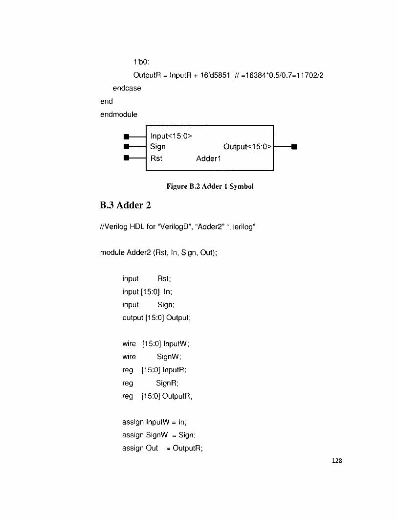
1'bO:
OutputR = InputR + 16'd5851; // =16384*0.5/0.7=11702/2
endcase
end
endmodule
lnput<15:0>
Sign 0utput<15:0>
Rst Adderl
Figure B.2 Adder 1 Symbol
B.3 Adder 2
//Verilog HDL for "VerilogD", "Adder2" Tlerilog"
module Adder2 (Rst, In, Sign, Out);
input Rst;
input [15:0] In;
input Sign;
output [15:0] Output;
wire [15:0] InputW;
wire SignW;
reg [15:0] InputR;
reg SignR;
reg [15:0] OutputR;
assign InputW = In;
assign SignW = Sign;
assign Out = OutputR;
128
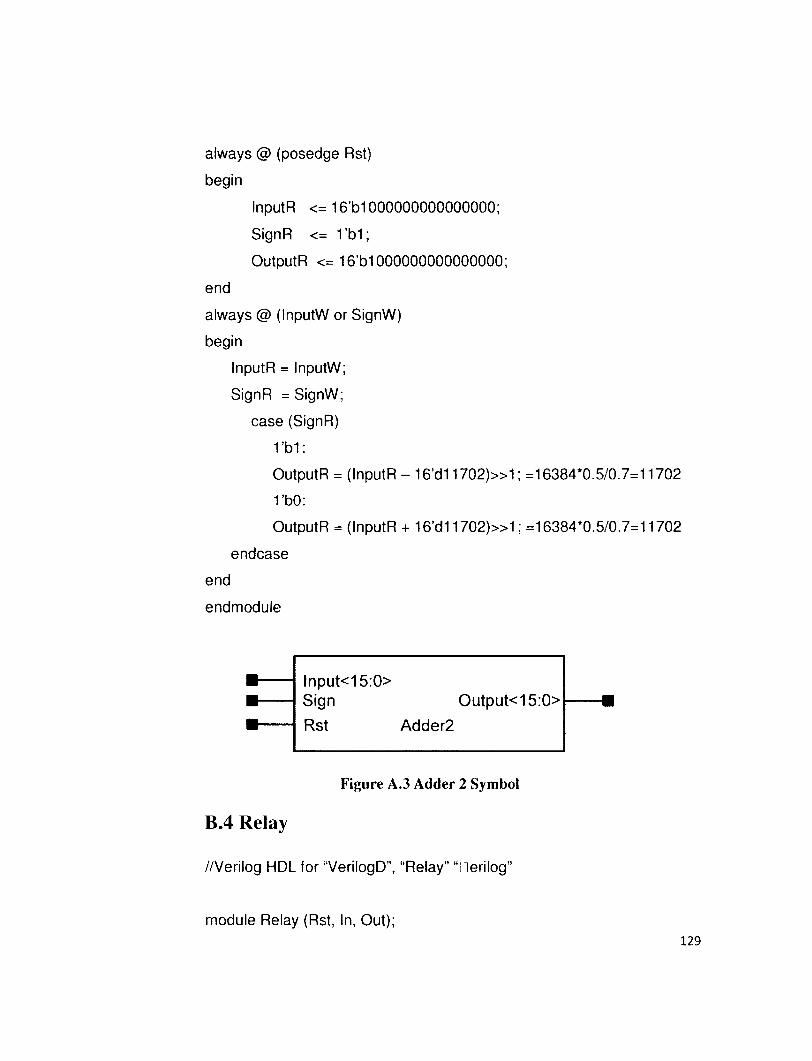
always @ (posedge Rst)
begin
InputR <= 16'b1000000000000000;
SignR <= 1'b1;
OutputR <= 16'b1000000000000000;
end
always @ (InputW or SignW)
begin
InputR = InputW;
SignR = SignW;
case (SignR)
1'b1:
OutputR = (InputR - 16'd11702)»1; =16384*0.5/0.7=11702
1'b0:
OutputR = (InputR + 16'd11702)»1; =16384*0.5/0.7=11702
endcase
end
endmodule
• lnput<15:0>
• Rst Adder2
0utput<15:0>
Figure A.3 Adder 2 Symbol
B.4 Relay
//Verilog HDL for "VerilogD", "Relay" "llerilog
module Relay (Rst, In, Out);
129

input Rst;
input [15:0] In;
output Out;
wire [15:0] Input;
reg Output;
assign Input = In;
assign Out = Output;
always @ (posedge Rst)
begin
Output <= 1'b1;
end
always @ (Input)
begin
Output <= (lnput[15]) ? 1 : 0;
end
endmodule
ln<15:0> Out
Rst
VDD Rel VDD Rel
VSS Relay notRel
Figure B.4 Relay Symbol
130

Appendix C VerilogA Source Code
C.l 16-bit Analog-to-Digital Converter
// VerilogA for Verilog_A, ADC_16b_Single, veriloga
'include "discipline.h"
"include "constants.h"
// Based on the OVI Verilog-A LRM, version 1.0 1996
// Ideal 16-bit Analog to Digital Converter
//
// vin: [V,A]
// vclk: [V,A]
// vd0..vd15: data output terminals [V,A]
//
// INSTANCE parameters
// tdel, trise, tfall = {usual} [s]
// vlogic_high = [V]
// vlogicjow = [V]
// vtrans_clk = elk high to low transition voltage [V]
// vref = voltage that voltage is done with respect to [V]
//
module ADC_16b_Single (vout, vin, vclk);
input vin, vclk;
output [15:0] vout;
electrical vin, vclk;
electrical [15:0] vout;
parameter real trise = 10p from [0:inf);
parameter real tfall = 10p from [0:inf);
parameter real tdel = 0 from [0:inf);
parameter real vlogic_high = 2.5;
parameter real vlogicjow = 0;
131

parameter real vtrans_clk =1.25;
parameter real vref = 2.5;
real unconverted;
real halfref;
real vd[0:15]; // vd[15:0]
integer i;
analog
begin
@ (initial_step ) begin
halfref = vref / 2;
end
@ (cross(V(vclk) - vtrans clk, 1))
begin
unconverted = V(vin);
for (i = (15); i >= 0 ; i = i -1)
begin
vd[i] = 0;
if (unconverted > halfref)
begin
vd[i] = vlogic_high;
unconverted = unconverted - halfref
end
else
begin
vd[i] = vlogiclow;

end
unconverted = unconverted * 2;
end
end
//
// assign the outputs
//
V(vout[15]) <+ transition( vd[15], tdel, trise, tfall)
V(vout[14]) <+ transition( vd[14], tdel, trise, tfall)
V(vout[13]) <+ transition( vd[13], tdel, trise, tfall)
V(vout[12]) <+ transition( vd[12], tdel, trise, tfall)
V(vout[11]) <+ transition( vd[11], tdel, trise, tfall)
V(vout[10]) <+ transition( vd[10], tdel, trise, tfall)
V(vout[9]) <+ transition( vd[9], tdel, trise, tfal
V(vout[8]) <+ transition( vd[8], tdel, trise, tfal
V(vout[7]) <+ transition( vd[7], tdel, trise, tfal
V(vout[6]) <+ transition( vd[6], tdel, trise, tfal
V(vout[5]) <+ transition( vd[5], tdel, trise, tfal
V(vout[4]) <+ transition( vd[4], tdel, trise, tfal
V(vout[3]) <+ transition( vd[3], tdel, trise, tfal
V(vout[2]) <+ transition( vd[2], tdel, trise, tfal
V(vout[1]) <+ transition( vd[1], tdel, trise, tfal
V(vout[0]) <+ transition( vd[0], tdel, trise, tfal
end
endmodule
133

rik .,! 0utput<15:0> Vin ADC 16b
Figure C.l 16-bit ADC Symbol
C.2 16-bit Digital-to-Analog Converter
// VerilogA for Verilog_A, DAC_16b_Single, veriloga
Include "discipline.h"
'include "constants.h"
// DAC_ldeal_168bit
//
// vin[0]..vin[15]: data inputs [V,A]
// vout: [V,A]
//
// INSTANCE parameters
// vref = reference voltage that conversion is with respect to [V]
// vtrans = transition voltage between logic high and low [V]
// tdel,trise,tfall = {usual} [s]
module DAC_16b_Single (vin, vout);
input [15:0] vin;
output vout;
electrical [15:0] vin;
electrical vout;
parameter real vref = 2.5 from [0:inf);
parameter real trise = 10p from [0:1 OOp);
parameter real tfall = 10p from [0:1 OOp);
parameter real tdel = 10p from [0:1 OOp);
134

parameter real vtrans = 1.25;
real out_scaled; // output scaled as fraction of 65536
analog begin
out_ _scaled = 0;
out. _scaled = out_ _scaled + (V(vin[15]) > vtrans) ? 32768 : 0);
out_ _scaled = out .scaled + (V(vin[14]) > vtrans) ? 16384 : 0);
out_ scaled = out. _scaled + (V(vin[13]) > vtrans) ? 8192 : 0);
out_ _scaled = out_ _scaled + (V(vin[12]) > vtrans) ? 4096 : 0);
out_ _scaled = out_ scaled + (V(vin[11 ]) > vtrans) ? 2048 : 0);
out_ _scaled = out_ _scaled + (V(vin[10]) > vtrans) ? 1024 : 0);
out_ scaled = out scaled + (V(vin[9J) > vtrans) ? 512 : 0);
out_ _scaled = out_ _scaled + (V(vin[8]) > vtrans) ? 256 : 0);
out_ scaled = out_ scaled + (V(vin[7]) > vtrans) ? 128 : 0);
out_ scaled = out _scaled + (V(vin[6]) > vtrans) ? 64 : 0);
out_ _scaled = out_ _scaled + (V(vin[5]> > vtrans) ? 32 : 0);
out_ _scaled = out_ _scaled + (V(vin[4]) > vtrans) ? 16 : 0);
out scaled = out_ scaled + (V(vin[3]) > vtrans) ? 8 : 0);
out_ _scaled = out_ _scaled + (V(vin[2]) > vtrans) ? 4 : 0);
out_ _scaled = out_ _scaled + (V(vin[1 ]) > vtrans) ? 2 : 0);
out _scaled = out_ _scaled + (V(vin[0]) > vtrans) ? 1 : 0);
V(vout) <+ transition( vref*out_scaled/65536, tdel, trise, tfall);
end
endmodule
Vin<15:0> DAC 16b
Vout
Figure C.2 16-bit DAC Symbol
135