design of practical fir filter using modified radix -4 ...€¦ · design of practical fir filter...
TRANSCRIPT
Page 227
Design of Practical FIR Filter Using Modified Radix-4 Booth
Algorithm
E Srinivasarao
M.Tech Scholar,
Department of ECE,
AITAM.
V. Lokesh Raju
Associate Professor,
Department of ECE,
AITAM.
L Rambabu
Assistant Professor,
Department of ECE,
AITAM.
Abstract:
Finite impulse response (FIR) filters are extensively
used in various digital signal processing applications
such as digital audio, image processing, data
transmission, biomedical etc. In some applications, the
FIR filter circuit must be capable to operate at high
sample rates, while in other applications, the FIR filter
circuit must be a low power circuit operating at
moderate sample rates. FIR filters design
implementation consist a large number of
multiplications, which leads to excessive area and
power consumption. The topology of the multiplier
circuit affects the resultant area and power
consumption. In this paper a new area efficient low
power FIR filter design is proposed using a carry look
ahead adder based modified Booth multiplier realized
in direct form. The practical filter coefficients are
determined after verifying different windowing
techniques using matlab. These coefficients are used
in design of area efficient design to improve the
efficiency of FIR filter. The design is implemented
using Xilinx 12.2 ISE tools, programming in Verilog
HDL.
Index Terms:
Finite impulse response (FIR) filters, modified Booth
encoding (MBE) scheme, VLSI design.
INTRODUCTION:
Digital filters are very important part of Digital Signal
Processing (DSP).
In fact their extraordinary performance is one of the
key reasons that DSP has become so popular.
Multiplication is the most basic function used in digital
filers. With advances in technology, various techniques
have been proposed to design multipliers, which offer
high speed, low power consumption and lesser area.
Thus making them suitable for various high speeds,
low power compact VLSI implementations. However,
these three parameters i.e. power, area and speed are
always traded off. Multiplication is the most basic
functions used in digital signal processing. It requires
more hardware resources and processing time than
addition and subtraction. In fact, 8.72% of all
instructions in a typical processing unit are multiplier.
Since multiplication dominates execution time, there is
a need for high speed multiplier.
In the past many novel ideas for multipliers have been
proposed to achieve high performance. Nowadays,
many finite impulse response (FIR) filter designs
aimed at either low area-cost or high speed or reduced
power consumption are developed. We can observe
that, with the increase in area, hardware cost of these
FIR filters are increasing. This observation leads me to
design a low area-cost FIR filter with the advantages
of reduced power consumption and moderate speed
performance. To reduce the hardware cost, the
hardware area should be optimized. In DSP, there are
essentially two sorts of channel, IIR and fir channel.
The motivation reaction of the IIR channel is of
unbounded span where as it is of limited term if there

Page 228
should arise an occurrence of fir channel .The fir
channel requires no criticism way and along these lines
it has no recursion and subsequently the fir channel is
non-recursive. Fir channels detail incorporate greatest
middle of the road stop band swell, pass band and stop
band edge recurrence. The coefficients of fir channel
require impressive measure of figuring’s. Along these
lines it is by and large performed by utilizing different
PC supported configuration apparatuses, for example,
channel outline and examination device of MATLAB.
So for a continuous applications, for example,
separating, combinational multipliers are utilized in
view of fast .the vast majority of the equipment many-
sided quality is because of multipliers, as channels
require expansive no of augmentation, prompting
extreme region, postpone and control utilization
regardless of the fact that executed in a full
exceptionally coordinated circuits now the issue
confronted is that how lessen the equipment
multifaceted nature of a multiplier. The principle
anxiety is on the lessening of multipliers in fir channel
the real impediment of higher request need.
The higher request forces more equipment necessities,
number-crunching operations, and territory use and
power utilization when outlining the channel.
Accordingly, minimizing or diminishing these
parameters is significant objective in advanced channel
outline assignment. It is yearning to discover
productive calculation that require as couple of math
operations as could reasonably be expected, as this in
the zone and minimizes the gadget size and vitality
utilization. To evacuate the repetitive calculation
which prompts more proficient calculations the
procedures picked are CSD, MB. This is utilized to
streamline the region of high pass fir channel. In CSD
structure the channel coefficients are settled. In CSD
structure multiplier region get lessened. MB is
essentially somewhat serial computational operation
that structures and inward result of a couple of vectors
in a one direct stride the upside of MB is its
productivity of mechanization.
Multipliers consume the most amount of area in a FIR
filter design. Product of two numbers has twice the
original bit width of the multiplied numbers. We can
truncate the product bits to the required precision to
reduce the area cost. Conventional multipliers are
replaced by a modified Booth multiplier here.
Modified Booth is twice as fast as Booth algorithm. It
produces only half the number of partial products
(PPs) when compared with an ordinary binary
multiplication. Modified Booth encoding (MBE)
scheme is identified as the most efficient Booth
encoding and decoding scheme. The truncation error
for a modified Booth multiplication is not more than 1
ulp (unit of last place or unit of least precision). So
there is no need of error compensation circuits.
Previous designs used transposed structure to realize
the FIR filter. Transposed structures are good for
cross-coefficient sharing. Also, as the filter order is
increasing, they will be faster. But, the area of delay
elements is larger. So, it is better to use direct form
structure for designing a low area-cost FIR filter. In
this brief, I present a new low area-cost FIR filter
design in VLSI using a modified Booth encoding
(MBE) scheme. Direct form is selected for FIR filter
realization. This brief is organized as follows. Design
of FIR filter is given in section II. The proposed design
is described in section III. Modified Booth multiplier is
described in section IV. Section V discusses about the
experimental results and comparisons. Finally,
conclusion is given in section VI.
DESIGN OF FIR FILTER
Generally, FIR filter can be expressed as
Where M represents the filter order, y [n] is the output
signal and ai represents the set of filter coefficients. If
x [n] is the input signal applied, x [n - i] terms are
referred as taps or tapped delay lines. Symmetric or
anti-symmetric coefficients can be considered for a
linear phase FIR filter.

Page 229
The implementation of a FIR filter requires three basic
building blocks – multiplication, addition, and signal
delay. Designing of FIR filter consists of four different
stages. Choose a suitable filter order ii. Find the
coefficients for the corresponding filter order iii.
Realize the filter using a suitable structure iv. Optimize
the area of the realized filter to the maximum extend
Fig 1: Direct form of FIR filter structure
Number of multiply-accumulate (MAC) operations
required increases linearly with the filter order.
Therefore, most of the designs used a minimum filter
order. Actually, slightly increasing the filter order
minimizes the total area. Then, filter coefficients
corresponding to the selected filter order must be find
out. Direct form or transposed form can be used for
realization of the FIR filter. Optimizing the area-cost
of FIR filter design to the maximum extend is the last
stage of the filter design.
PROPOSED DESIGN
A system’s performance is determined by the
performance of the multiplier because the multiplier is
generally the slowest element in the system. So, a
modified Booth multiplier is suggested since it saves
more area and it is faster than other conventional
multipliers. The proposed new low area-cost FIR filter
using a modified Booth multiplier is shown in Fig. 2.
A direct form filter is such that at each clock cycle a
new data sample and the corresponding filter
coefficient can be applied to the multiplier’s inputs.
x[n] is given as the input signal. D-FFs are used as the
delay elements. Modified Booth multiplier block is
provided for multiplying the input signal with the set
of filter coefficients corresponding to the selected filter
order.
Then, modified Booth multiplier block will provide the
output signal y[n].
Fig 2: Practical FIR filter
Proposed Methodology
Block Diagram
Fig 3: Practical FIR filter
Flow Chart

Page 230
Realization
Fig 4: Realization filter
FLOATING POINT FORMAT
Floating point representation works well for numbers
with large dynamic range based on the no. of bits. This
standard is almost exclusively used across computing
platforms and hardware designs that support floating
point arithmetic. In this standard a normalized floating
point number x is stored in three parts: the sign s , the
excess exponent e ,and the significant or mantissa m,
and the value of the number in terms of these parts is:
bee mx
2**1*)1(
The format is written with the significant having an
indirect integer bit of value 1 (except for special data,
see the exponent encoding below). With the 52 bits of
the fraction significant become visible in the memory
format, the total precision is therefore 53 bits. The bits
are laid out as follows:
From the MATLAB command window the real filter
coefficients are 0.0038,-0.035, -0.2278, 0.610, 0.0037,
-.0331, -0.2291.these filter coefficients are converted
to double precision floating point number. The
converted coefficients are
0.003775018138711,
-0.033541428579110,
-0.227792539932163,
0.618026583319437,
-0.229088808118480,
0.033110787270075,
0.003737449345339.
The Qn,m format of an N bit number sets n bits to the
left and m bits to the right of the binary point. In case
of signed numbers, the MSB is used for the sign and
has negative weight. A two’s complement fixed point
number in Qn,m format is equivalent to b=bn-1bn-2bn-3bn-
4……b2b1b0b-1……b-m. With equivalent floating point
value:-bn-12n-1
+bn-22n-2
+…..+b121+b0+b-12
-1+…..b-m2
-m.
A floating point number format is simply converted to
Qn,m fixed point format by bringing m fractional bits
of the number to the integer part and then dropping the
rest of the bits with or without rounding. This
conversion translates a floating point number to an
integer number with an implied decimal the implied
decimal needs to be remembered by the designer for
referral in further processing of the number in different
calculations:
Num_fixed = round(num_float*2m)
Or
Num_fixed = fix(num_float*2m)
The coefficients are converted to double precision
floating number into fixed point format.the coefficients
are in decimal numbers that are 124,-1099,-
7464,20252,-7507,-1085,123.these decimal numbers
are converted to binary then hexadecimal number.
CSD ALGORITHM
The CSD code is a ternary number system with the
digit set {1¯ 0 1}, where 1¯ stands for 1. Given a
constant, the corresponding CSD representation is
unique. CSD representation of a number can be
recursively computed using the string property and has
two main properties:
(1)The number of nonzero digits is minimal
(2) No two consecutive digits are both nonzero, that is,
two nonzero digits are not adjacent.
The first property implies a minimal Hamming weight,
which leads to a reduction in the number of additions
in arithmetic operations. The second property provides
its uniqueness characteristic. However, if this property
is relaxed, this representation is called the minimal

Page 231
signed digit (MSD) representation, which has as many,
nonzero as the CSD representation, but which provides
multiple representations for a constant. It enables the
reduction of the number of partial products that must
be calculated fast and also low-power consumption
and low area structure of a multiplier for DSP
applications or self-timed circuits. From the practical
point of view, the traditional approach to generate the
CSD representation. All of these algorithms generate
the CSD code recursively from the least significant bit
(LSB) to the most significant bit (MSB). CSD
representation of an integer number is assigned and
unique digit representation that contains no adjacent
non zero digits. Given an n-digit binary unsigned
number X={x0, x1, - - - - - - - , x1n} expressed as
X = 1}1,0{,2.1
0
i
in
n
i xx
Then the (n+1)-digit CSD representation Y= {y0, y1,_
_ _ _ _ _ _ _ yn
} of X is given by
Y = 2}1,0,1{,2.2.0
1
0
i
in
i
i
in
i
i yyx
The condition that all non-zero digits in a CSD number
are separated by zero implies that
310,0.1 niyy ii
From this property, the probability that a CSD n-digit
has a non-zero value is given by
P 4])2/1(1[9/13/1)1 n
i ny
As n becomes large, this probability tends to 1/3 while
this probability becomes ½ in a binary code. Using this
property, the number of additions/subtractions is
reduced to minimum in multipliers and as a result, an
overall speed –up can be achieved. Encoding 2 is
prefer- able since it satisfies the following relation.
5s
i
d
ii yyy
Where y s
i represents the sign bit and y d
i the data bit.
This encoding also allows an additional valid
representation of 0 when y s
i=1 and y d
i=1, which is
useful in some arithmetic implementations. In the
whole paper, this encoding is used.
CSD representation for binary form:
h(0)=124 =0000 0000 0111 1100=0000 0000
1000 01 00(CSD form)
h(1)=1099=0000 0100 0100 1011=0000 0100
0101 01 01 (CSD form)
h(2)=7464=0001 1101 0010 1000=0010 01 01
0010 1000(CSD form)
h(3)=20252=0100 1111 0001 1011=0101
0001 0010 01 01 (CSD form)
h(4)=7507=0001 1101 0101 0011=0010 01 01
0101 0101 (CSD form)
h(5)=1085=0000 0100 0011 1101=0000 0100
0100 01 01(CSD form)
h(6)=123 =0000 0000 0111 1011=0000 0000
1000 01 01 (CSD form)
Xn(0)*h(0)+xn(1)*h(1)+xn(2)*h(2)+xn(3)*h(3)+xn(4)
*h(2)+Xn(5)*h(1)+xn(6)*h(0)
MODIFIED BOOTH MULTIPLIER
Modified Radix-4 Booth’s Algorithm is made use of
for fast multiplication. The salient feature of this
algorithm is only n/2 clock cycles are needed for n-bit
multiplication as compared to n clock cycles in
Booth’s algorithm. This type of multiplier operates
faster than an array multiplier for longer operands
because its computation time is proportional to the
logarithm of the word length of operands. Booth
multiplication is a technique that allows for smaller,
faster multiplication circuits, by recoding the numbers
that are multiplied. Modified Booth multiplier consists
of Booth algorithm, including Booth encoder and
Booth decoder, Wallace tree compressor (WTC) and
carry look-ahead adder (CLA). Architecture of the
modified Booth multiplier is shown in Fig. 2.
Multiplicand X and multiplier Y are the external inputs
for Booth algorithm. Usually, a multiplication includes
a generation of the PPs, addition of the generated PPs
until the last two rows are remained and then
computing the final multiplication result by adding the
last two rows.

Page 232
Fig 5: Architecture of modified Booth multiplier
Multiplicand bits are divided into a combination of
two bits each with overlapping after appending a zero
at the LSB of the multiplicand X. Xi-1 represents the
appended zero term. Overlapping is done by the MSB
of the group on the right side with the LSB of the
group on the left side when two adjacent groups are
considered. Grouping of multiplicand bits is shown in
Fig. 3. The 8-bit multiplicand term is represented as
X7 X6 X5 X4 X3 X2 X1 X0. If the first three bit
combination selected is X1 X0 Xi-1, then the next
three bit combination will be X3 X2 X1 and so on. The
grouping of the multiplier bits is shown in Fig. 4.
Multiplier Y is divided into a combination of three bits
each with overlapping after appending a zero at the
LSB of multiplier Y. Yi-1 is the appended zero bit.
Overlapping is done by the MSB of the group in the
right side with the LSB of the group in the left side
when two adjacent 3-bit combinations are considered.
The 8-bit multiplier term is represented as Y7 Y6 Y5
Y4 Y3 Y2 Y1 Y0. If the first three bit combination
selected is Y1 Y0 Yi-1, then the next three bit
combination will be Y3 Y2 Y1 and so on. Each 3-bit
combination of the multiplier bits is given to a Booth
encoder as shown in Fig. 4. The Booth encoder
generates the encoded signals for each 3-bit
combination of the multiplier Y. The logic diagram of
the Booth encoder is shown in Fig. 6. From the truth
table given below in table I, the encoded signals of any
3-bit combination of multiplier input can be found out.
These encoded signals along with the each 2-bit
combination of multiplicand bits are then given to a
Booth decoder.
Booth decoder generates the PPs from the encoded
signals and multiplicand bits.
Fig. 6: Logic diagram of Booth encoder
The number of PPs generated by the modified Booth
multiplication is exactly half the number of PPs
generated by the binary multiplication. Each step is
slightly more complex compared to the simple
multiplier, but is almost as fast as the basic multiplier
stage that it replaces. For an 8 × 8 multiplication, the
number of PPs generated in a binary multiplication is
64. Therefore, only 32 PPs will be produced by the
modified Booth multiplier. An example of modified
Booth multiplication is given in Fig. 5. Let the two 8-
bit numbers be 10011001 and 01100110. Each of the
3-bit combination of multiplier 01100110 starting from
LSB is multiplied with each of the 2-bit combination
of the multiplicand 10011001. Therefore, a total of 32
PPs are generated. So, the 64 PPs generated in binary
multiplication are reduced to 32 PPs in modified Booth
multiplication. Hence, area-cost of the filter design
will be reduced. The PPs generated by the Booth
decoder are then given to a Wallace tree structure.
Wallace tree reduction always compresses the partial
product bits. Wallace tree has been used in order to
accelerate multiplication by compressing the number
of partial products. Wallace Tree Structure can be
made by using compressors, full adders and various
other techniques. WTC is a technique used to increase
the speed of partial product addition operation. A
WTC shown in Fig. 8 consists of a set of full adders
(FAs). Sometimes, the FA at LSB is replaced by a half
adder (HA). The HA adds two input bits to produce
one sum bit and one carry bit. All the FAs add three
input bits at a time to produce one sum bit and one
carry bit.

Page 233
Therefore, the PPs are added in parallel using the
WTC until two sequences of outputs are generated.
One is a sequence of sum bits and the other is a
sequence of carry bits. A WTC would save most of the
area since it produces only two outputs. Since the
addition of PPs is done in parallel, the operation of
WTC is fast also. The full adders and half adders
replaced by the different compressors speeds up the
summation in general and multiplication in particular.
Fig 7: Logic diagram of Booth decoder
Example of modified Booth multiplication
Wallace tree compressor finally, these sequences of
sum bits and carry bits are given to a CLA. The CLA
provides another speed boost to the system. They are
the fastest adders. CLA consists of a set of full adders.
A CLA shown in Fig. 8 is identical to the half adder
except that it has an additional input, Cin, so that a
carry from a previous addition may be passed along.
Furthermore, instead of a carry out, Cout, propagate
(P) and generate (G) signals are produced.
Si = Ai xor Bi xor Cin - (2)
Pi = Ai xor Bi - (3)
Gi = Ai × Bi - (4)
Ci+1 = Gi + Pi Ci - (5)
Fig 8: Carry look-ahead adder
CLA calculates the carry signals in advance, based on
the input signals. Carry generate and propagate signals
only depend on the input bits.
The carry bits can be computed in parallel with the
sum bits, which increases the speed of the adder
compared to a ripple style adder. CLA is used to avoid
the rippling carry present in ripple carry adder (RCA).
Because, rippling carry produces an unnecessary delay
in the circuit. CLA uses the concepts of generating and
propagating the carry and it produces the final output
and this is the output of the FIR filter. Modified
Booth’s algorithm is twice as fast as Booth’s
algorithm. The modified Booth algorithm is
extensively used for high-speed multiplier circuits. The
drawback of MBE scheme is that as the number of
stages increases, the area and power consumption will
also increase.
RESULTS AND COMPARISONS
We implemented three FIR filters for comparison with
the previous design approaches. One FIR filter is
designed using an older version of truncated
multiplier, one using faithfully rounded truncated
multiple constant multiplication/ accumulation
(MCMAT), and one using modified Booth multiplier.
ModelSim is the software used for simulation and
Xilinx 12.2 software is used as the synthesis tool. After
logic synthesis, all the designed systems are
implemented on the Xilinx Spartan II FPGA. The
simulation results for the three FIR filters obtained are
shown in following section. A detailed comparative
study is done in order to analyze how much the
designed low area-cost FIR filter using modified Booth
multiplier is better than the conventional existing FIR
filter designs. The comparison is done in terms of area,
delay, power consumption and memory usage.
Comparison between design summaries obtained from
the Xilinx software for the three FIR filters designed
are shown in table II. The area consumption of the
FIR filters is noted with the help of the area report,
which is available as a part of the synthesis report
while implementing in the Spartan II FPGA. The
number of slices utilized among the available 1728
slices in the Spartan II FPGA is taken for the
comparison.
Page 234
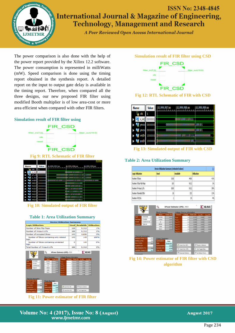
The power comparison is also done with the help of
the power report provided by the Xilinx 12.2 software.
The power consumption is represented in milliWatts
(mW). Speed comparison is done using the timing
report obtained in the synthesis report. A detailed
report on the input to output gate delay is available in
the timing report. Therefore, when compared all the
three designs, our new proposed FIR filter using
modified Booth multiplier is of low area-cost or more
area efficient when compared with other FIR filters.
Simulation result of FIR filter using
Fig 9: RTL Schematic of FIR filter
Fig 10: Simulated output of FIR filter
Table 1: Area Utilization Summary
Fig 11: Power estimator of FIR filter
Simulation result of FIR filter using CSD
Fig 12: RTL Schematic of FIR with CSD
Fig 13: Simulated output of FIR with CSD
Table 2: Area Utilization Summary
Fig 14: Power estimator of FIR filter with CSD
algorithm

Page 235
Simulation result of FIR filter using modified Booth
multiplier
Fig 15: RTL Schematic of FIR filter with MBM
Fig 16: Output of FIR filter with MBM
Table 3: Synthesis report of FIR filter with MBM
Fig 17: Power estimator of FIR filter MBM
Comparison of Results the Above Three
Techniques
Table 4: Comparison of results in terms of power,
area and delay
Parameter FIR FIR
WITH
CSD
FIR
WITH
MBM
Area(slices) 128 1918 1757
Area(LUT’s) 188 3659 3381
Delay(ns) 18.14 41.68 7.58
Power(mw) 305 286 244
Power*delay 5532.7 11920.48 1849.52
Comparison of Design Summaries
Our new FIR filter is more efficient in terms of power
consumption also. Even though the delay of our
proposed design is less when compared with the
previous designs, the delay of our designed filter is
moderately a large value. But, we focus on a low area-
cost FIR filter design with moderate speed
performance for mobile applications where area and
power are our important design considerations.
Memory usage of both the previous FIR filters remains
the same. But, the memory usage of our new area
efficient FIR filter is increased.
CONCLUSION
The FIR filters are extensively used in digital signal
processing and can be implemented using
programmable digital processors. Digital signal
processing has become increasingly popular over the
years with the advancement in VLSI technology. The
high speed realization of FIR filter with less power
consumption has become much more demanding. In
this project, the practical FIR high pass filters is
designed by using hamming window and obtained the
frequency response and coefficients using MATLAB.
After obtaining the response, the FIR filter is realized
and implemented in VLSI domain. The direct form
architecture consists of adders, multipliers and delay
elements. In VLSI normal multiplication of two
numbers consumes more power so instead of direct
multiplication of input with the coefficients.

Page 236
The CSD,MBM and DA algorithm are used for
multiplication process and obtained less power
consumption. Separately CSD, MBM and DA
algorithms are applied for multiplication process and
compared two techniques in terms of power. From the
comparison of above two techniques it is concluded
that DA based algorithm is a best technique for
reducing power consumption because of LUT’s are
used in DA algorithm. Moreover the simulation and
synthesis results are analyzed using Xilinx 12.2 ISE.
REFERENCES
[1].A. Avizienis, “Signed digit number representation
for fast parallel arithmetic,” IRE Transactions on
Electronic Computers, 1961, vol. 10, pp. 389 400.
[2]. R. Hashemian, “A new method for conversion of a
2’s complement to canonic signed digit number system
and its representation,” in Proceedings of 30th IEEE
Asilomar Conference on Signals, Systems and
Computers, 1996, pp. 904 907.
[3]. H. H. Loomisand B. Sinha, “High speed recursive
digital filter realization,” Circuits, Systems and Signal
Processing, 1984, vol. 3, pp. 267 294.
[4]. K. K. Parhi and D. G. Messerschmitt, “Pipeline
interleaving parallelism in recursive digital filters. Pt I:
Pipelining using look ahead and decomposition,” IEEE
Transactions on Acoustics, Speech Signal Processing,
1989, vol. 37, pp. 1099 1117.
[5]. K. K. Parhi and D. G. Messerschmitt, “Pipeline
interleaving and parallelism in recursive digital filters.
Pt II: Pipelining incremental block filtering,” IEEE
Transactions on Acoustics, Speech Signal Processing,
1989, vol. 37, pp. 1118 1134.
[6]. A. V. Oppenheim and R. W. Schafer, Discrete
time Signal Processing, 3rd, 2009, Prentice Hall.
[7]. Y. C. Lim and S. R. Parker, “FIR filter design over
a discrete powers of two coefficient space,” IEEE
Transactions on Acoustics, Speech Signal Processing,
1983, vol. 31, pp. 583 691
.
[8]. H. Samueli, “An improved search algorithm for
the design of multiplier less FIR filters with powers of
two coefficients,” IEEE Transactions on Circuits and
Systems, 1989, vol. 36, pp. 1044 1047.
[9]. J. H. Han and I. C. Park, “FIR filter synthesis
considering multiple adder graphs for a coefficient,”
IEEE Transactions on Computer Aided Design of
Integrated Circuits and Systems, 2008, vol. 27, pp. 958
962.
[10]. A. G. Dempster. and M. D. Macleod, “Use of
minimum adder multiplier blocks in FIR digital
filters,” IEEE Transactions on Circuits and Systems II,
1995, vol. 42, pp. 569 577.
[11]. R. I. Hartley, “Sub expression sharing in filters
using canonic signed digit multipliers,” IEEE
Transactions onCircuits and Systems II, 1996, vol. 43,
pp. 677 688.
[12]. Y. Jang. and S. Yang, “Low power CSD linear
phase FIR filter structure using vertical common sub
expression,” Electronics Letters, 2002, vol. 38, pp. 777
779.
[13]. A. P. Vinod, E. M. K. Lai, A. B. Premkuntar and
C. T. Lau, “FIR filter implementation by efficient
sharing of horizontal and vertical sub expressions,”
Electronics Letters, 2003, vol. 39, pp. 251 253.
[14]. A. Hosnagadi, F. Fallah and R. Kastner,
“Common sub expression elimination involving
multiple variables for linear DSP synthesis,” in
Proceedings of 15th IEEE International Conference on
Application specific Systems, Architectures and
Processors, Washington 2004, pp. 202 212.
[15]. P. K. Meher, S. Chandrasekaran and A. Amira,
“FPGA realization of FIR filters by efficient and
Page 237
flexible systolization using distributed arithmetic,”
IEEE Transactions on Signal Processing, 2008, vol.
56, pp. 3009 3017.
Author Profile:
Etcherla srinivasarao presently pursuing his M.Tech
in VLSI system design in Electronics and
Communication Engineering Department, AITAM,
Tekkali. His areas of interest are Low Power VLSI
system design and digital filter optimization. He has
attended for one national level workshop. He is
membership in GSM IEEE. The author may be
reached at [email protected]
V. LokeshRaju presently working as Associate
Professor in Electronics and Communication
Engineering Department, AITAM, Tekkali. He has 12
years experience in teaching and research. Now he is
doing Research in Reconfigurable Antennas also. He
published more than 10 research papers in National/
International Journals and Conferences.
L.Rambabu presently working as Assistant Professor
in Electronics and Communication Engineering
Department, AITAM, Tekkali. He has 9 years
experience in teaching. He published 5 research papers
in National/ International Journals and Conferences.