design of out phasing power amplifier based on ldmospaper.ijcsns.org/07_book/201707/20170744.pdf ·...
TRANSCRIPT

IJCSNS International Journal of Computer Science and Network Security, VOL.17 No.7, July 2017
306
Manuscript received July 5, 2017 Manuscript revised July 20, 2017
Design of out phasing Power Amplifier Based on LDMOS
Mohsen. Pooya1, Farbod. Setoudeh2, Mohammad Bagher Tavakoli1
1Department of Electrical Engineering, Arak Branch, Islamic Azad University, Arak, Iran
2Department of Electrical Engineering, Arak University of Technology, Arak, Iran Abstract The intention of this work was to design a power amplifier at 400-900MHz based on LDMOS (Lateral Double diffused MOS) technology and to analyze the behavior of the design considering memory effects and nonlinear distortions. The MRF6V3090N and two MRFE6VP8600H RF power transistors used in this procedure. The designing composed of a highly linear power amplifier which attained the best gain, Inter modulation Distortion (IMD) and Power Added Efficiency (PAE).These optimizations and Load-pull analysis were utilized in the Agilent Design System (ADS) simulations. The design showed a mismatch problem at the output and high self-heating, at the DC bias network. After a modifications, the PA showed a proper gain of 45dB.We used the non-ideality of ADS model, internal feedback and the big size of the transistor in the package at the frequency bandwidth caused a mismatch at the output. We tried redesigning the PA using ADS, notwithstanding the non-ideality of the model, adjustments have been added to improve the matching and bias networks performance. The design represented an improved gain of 46 dB near the P1dB compression point, however the achieved gain at that point, seems a little lower. The ADS simulations and measured results were used in this process. The design demonstrated a intermodulation distortion and by changing the bias operation, the IMD3 rejection was calculated with ACPR(Adjacent Channel Power Ratio), the ratio between the total power adjacent channel to the main channel's power in the range of -29 to -54dBc which is a good value regarding the standards. The Power Added Efficiency (PAE) of (40-68)% was shown from 450 to 860 MHz in this work. Despite the output mismatch problem at the matching network, this LDMOS transistor has shown a good performance values comparable with the other technologies. Keywords: Amplifier,LDMOS,PAE,Pout,ADS,Simulation,Intermodulation,gain,frequency,DC bias,Load Pull,ACPR.
1. Introduction
In the amplifiers to reach a specified gain or output power necessity, multiple stages composed of one or more transistors are usually required. The final stage generally has low gain, for this purpose, the preamplifier at the first stage increase overall output gain. The Amplifiers are commonly designed for operation in a determined bandwidth such as the transmitters band, and ideally have a constant gain over the bandwidth. LDMOS transistor, in specific, used for power amplifier applications at RF and have a number of benefits such as: good gain linearity,
better intermodulation distortion performance, flat saturation, easy bias circuit networks, high over drive output power capability. In the RF systems such as transmitters, Amplifier is the most important part and optimized for improve the transmission of signals [1]. In fact, it is utilized to modify the signal for improved transmission of signal [1]. The LDMOS RF transistors commonly amplified signals in the communication systems [1]. In this device, Shorter channel length improves the transistor linearity which always works in velocity saturation [1].The use of LDMOS has enhanced because of its awesome features of gain, stability, linearity and wide range of frequency in UHF[2]. This study describes two stage amplifiers; Pre-amplifier and Power stage composed of the LDMOS transistors, DC bias network, microstrip lines, baluns and capacitors. The PA shows average gain of 35 to 58dB over a bandwidth of 500 MHz ranging between 400 and 900MHz. Reviewing other literatures: Kaldi Li and his partners, worked on” A 40w Ultra Broadband LDMOS Power Amplifier”[2].They utilized a two part broadband balun impedance transformer with ferrite beads which allow the device to operate at low frequency down to 2MHz, and a series R-C feedback loop to optimize the gain[2].They used it in small cell communication and mobile systems[2].But 19dB gain,30%PAE and -30dBc ACPR is low at 2-800MHz for DVB-T applications [2].Also, several narrow band amplifiers are applied to increase the bandwidth, but LDMOS decrease the size and cost in the base station usage[3].Except the characteristics of dynamic device, impedance matching also affect the structure of the broadband UHF amplifier[3]. Often, its output power is high in the stations, as regards a low loss outcome in large power dissipation [3]. The Matching network works as an important component for increased bandwidth linearity and the gain in the power amplifiers [3].Dajie Dae et al., achieved to ”A 10w Broadband Power Amplifier for Base Station ”applications[3]. They apply multiple LC matching networks and output impedance that consist multi-part composed of microstrip lines and capacitors for increase the bandwidth. [3].They attained 14.5dB gain, 50%PAE and -33dBc ACPR at 1.8-2.0GHz.[3]. Lei Zhao, et al., presented “A 20 Watt, Two-stage, Broadband LDMOS Power Amplifier IC in PQFN8×8 Package at 2 GHz for Wireless Applications” at 1.7 to 2.3GHz.[4] The two-stage, single-chip design exhibits 32 dB of gain,PAE of 50% and -63dBc ACPR for macro cell and small cell usages[4]. It seems gain
IJCSNS International Journal of Computer Science and Network Security, VOL.17 No.7, July 2017 307
is low for digital TV terrestrial and should be better. David et al., designed “A 25 W, 2.3 to 2.7 GHz Wideband LDMOS Two-stage RFIC Power Amplifier for Driver and Small-cell Doherty Application” [5]. A 25 W, dual-path, two-stage wideband RFIC power transistor envelope 2.3 to 2.7 GHz attained 30 dB gain,40%PAE and -55dBc ACPR[5]. We try to increase favor gain at UHF band. Zhang et al., presented “A 72% PAE, IO-Watt, CMOS-LDMOS Switch-Mode Power Amplifier for Sub-l GHz Application” [6]. The measurement results offer that the proposed accedes a power-added efficiency greater than 72.6% from 450MHz to 1000MHz with an output a power gain greater than 26.5dB[6] PAE is good, But Adjacent Power Ratio is not calculated and It is essential in DVB-T amplifier. Srinidhi et al., represented A 400 W 2-Way Asymmetrical Doherty PA with 50% Efficiency based on Second-Generation Air fast LDMOS technology [7]. The 2-way asymmetric minimum-phase Doherty PA is designed for 2110-2170 MHz band rendering 50% PAE and 17dB gain for LTE, WCDMA and TD-SCDMA usage systems. [7].The gain is low, ACPR value does not exist and It is not suitable for Our work. Another methods have been utilized to attain the desired frequency response, gain flatness, better PAE and reduce IMD3 can be used in cases such as: Impedance inversion which has an output capacitor modification and improve of passive broadband signal [8]. Qureshi et al., proposed A 700-W Peak Ultra-Wideband Broadcast Doherty Amplifier [8]. A wideband high-power Doherty design technique providing aliquot bandwidths >50% is explained. It utilizes wideband impedance inversion, device output capacitance restitution and passive phase-optimum wide band input-signal splitting [8]. As prove of concept a LDMOS based uItra-wideband broadcast Doherty amplifier is offered, which covers the UHF-TV 470MHz-803MHz band with IMD between 40%-48% , PAE between 38%-47% and 16dB gain [8]. In the DVB-T/T2 aplications, optimize linear gain flatness is very important and essential for UHF frequency conturs.[8]. M. Hayati et al., designed and executioned A Broadband Doherty Power Amplifier with Harmonic Suppression [9]. The advised DPA has main benefits in items of the linearity and works on a wideband frequency range (2.1 – 2.7 GHz) with 10 dB gain, minimum 40% PAE, and -40dBc ACPR used in base stations.[9]. It should be tried to increase gain in UHF DVB-T power amplifier on the TV stations. Yao et al., presented a novel Four Stage 200W Doherty Power Amplifier for DVB-T (Digital Video Broadcasting Terrestrial) Transmitter [10]. Two push-poll LDMOS are utilized as the carrier amplifier and peak amplifiers with the transmission lines load network to form a symmetric four-stage Doherty PA with 20dB gain ,PAE of 55%, and -30dBc ACPR at UHF band was attained. [10].Gain is good but it’s not enough. Mikkel et al., suggested Band-Split Forward-Path Cartesian Feedback for Multicarrier TETRA RF Power Amplifiers [11]. ACPR in the -80dBc, 27%PAE and
26dB gain for telecommunication systems such as WCDMA are presented.[11] .IMD3 rejection is very good but PAE and gain are low. Estor et al., described Design Method for UHF Class-E Power Amplifiers [12]. The design process Amplifiers with Si-LDMOS, SiC-MESFET, GaN-HEMT on a Si substrate, and GaN-HEMT on a Sic substrate produce. The PAE greater than 75% and gain between 13 dB and 17 dB [12]. Gain is low, IMD rejection is not calculated and our paper technology are LDMOS. Takaya et al., presented Doherty Power Amplifier with Asymmetrical Drain Voltages for Enhanced Efficiency at 8 dB Backed-off Output Power [13]. The DPA is designed using a push-pull (LDMOS) for an ultra-high frequency (UHF) band Measurement results signal, show a PAE of 50%, 20 dB gain and -23dBc ACPR is utilized for wireless telecommunication systems for mobile phones, wideband code division multiple access (WCDMA) And high-transmission-data-rate services [13]. But gain and IMD are low for DVB-T/T2 values. Qian et al., presented A 35 dBm Output Power and 38 dB Linear Gain PA With 44.9% Peak PAE at 1.9 GHz in 40 nm CMOS [14]. They built linear PA that improves efficiency and achieved to 38dB gain,44.9% PAE and -35.8dBc ACPR at 1.9 GHz in 40 nm CMOS[14] . Luca Piazzon et al. worked at A Method for Designing Broadband Doherty Power Amplifers.[15].A Doherty broadband Power Amplifier proposed based on couplers, input splitter and output combiner.[15].They achieved 10dB gain, more than 41% PAE and better than -30dBc ACPR at 2GHz in GaN technology[15]. Changhyun Lee and Changkun Park presented at A 2.4 GHz CMOS Power Amplifier with Mode-Locking Structure to Enhance Gain.[16]. They optimized and achieved 23dBm Output power and 34.9% PAE at 2GHz by a mode-locking method for the cascode structure of an RF CMOS power amplifier.[16]. Y. Shang et al. proposed The Design and Thermal Reliability Analysis of a High-Efficiency K-Band MMIC Medium-Power Amplifier with Multi harmonic Matching[17].They attained 22dB-27dB gain,34%-38% PAE at 24-28GHz frequency by using multiharmonic matching design in GaAs pHEMT technology.[17]. Xiaofan Chen, et al. presented A Broadband Doherty Power Amplifier Based on Continuous-Mode Technology [18]. They designed 52%–66% efficiency,6dB to 13dB gain at 1.65GHz to 2.75GHz and -45dBc to -55dBc ACPR after DPD at continuous-mode technique in a Doherty power amplifier.[18]. Alessandro Cidronali, et al., presented Frequency Analysis and Multiline Implementation of Compensated Impedance Inverter for Wideband Doherty High-Power Amplifier Design.[19].They achieved an average drain efficiency between 37% and 47%, with an average power of 49 dBm across 37.5% in the 650–950-MHz band.[19]. Dong et al., discussed the integration of Class-J power amplifiers in Standard CMOS Technology [20]. The proposed a 3.3 V supply, achieves a (PAE) of 43.7% and 45.1%, with a maximum gain of 17.4 dB and

IJCSNS International Journal of Computer Science and Network Security, VOL.17 No.7, July 2017 308
better than -30dBc ACPR from 2.1 GHz to 4.8 GHz.[20]. Hallberg, et al., proposed A Doherty Power Amplifier Design Method for Improved Efficiency and Linearity.[21]. They achieved 16dB gain, 40%PAE and -41dBc ACPR.[21]. Hur, et al., presented A Multi-Level Class D CMOS Power Amplifier for an Out-Phasing Transmitter with a Non-Isolated Power Combiner.[22].They achieved 21dB peak power, 45% PAE at 500-750MHz in a standard 0.18-μm CMOS process..[22]. Jang, et al., proposed a Broadband Almost-Digital RF Transmitter with an Efficient Power Amplifier [23]. They reached 40% PAE, ACPR between −26dBc and −37dBc dB, 13dB to 36dB gain at 700MHz -1.1GHz.[23].Kihyun Kim, et al. implemented A Two-Stage Broadband Fully Integrated CMOS Linear Power Amplifier for LTE Applications.[24].They achieved PAE of 26.1% – 33% , -30 dBc ACPR and 15dB gain in standard 0.11 μm RF CMOS technology at 1.8 to 2.3 GHz.[24]. Hwiseob Lee, et al. Optimized Current of the Peaking Amplifier for Two-Stage Doherty Power Amplifier.[25].They obtained 25dB gain, 56.8% PAE and −25 dBc adjacent channel leakage power ratio (ACLPR).[25]. Mustafa Özen, et al. proposed A Symmetrical Doherty Power Amplifier with Extended Efficiency Range [26]. They obtained PAE of %50, adjacent power leakage ratio of -49 dBc, 5dB to 14dB gain at 1.8-2.5GHz.[26]. Pang et al., Designed of continuous-mode GaN power amplifier with compact fundamental impedance solutions on package plane.[27].They measured 10 dB gain, 55.8%–74.1% PAE and around −30 dBc ACPR at 500MHz-4GHz.[27]. Qi et al., presented the Third-octave power amplifier using ring based matching network with high efficiency [28]. They achieved PAE over %48, 9.5dB− 11.5 dB power gain at frequency range 0.5GHz −4.4GHz.[28]. Taghavi et al., designed a Sequential Load-pull Technique for Multi-octave Design of RF Power Amplifiers [29]. They reached to drain efficiency of 53% - 64%, gain of 8dB-13dB, in the range of 0.7 – 4.0 GHz [29]. Wu, et al., presented Analysis and Design of an Ultra broadband Stacked Power Amplifier in CMOS Technology [30].They achieved PAE of 13%–20%, gain of 10dB-20dB and -25dBc to -50dBc ACPR.[30]. Quality factor is very important for broad band pre-amplifier and power amplifiers. It’s determining the size of bandwidth What ratio of the resonator frequency bandwidth, We designed with the lowest amount of Q-Factor acceptable and Linear UHF bandwidth [31-40], In design we utilized optimum capacitors and micro strip Lines. In total bandwidth gain is obtained better than 40dB. According the circuit design, in the UHF broadband gain is fix, flat and linear. PAE specified the effect of Amplifier gain and percent of different output to input power divided dc power. We achieved 40%-68%PAE.The Non linearity Power Amplifiers make IMD signals including two or more different frequencies. In this paper, We decrease IMD signals or adjacent channel leakage power ratio at 400-
900MHz between -29 to-54dBc also we used two-stage amplifier with three LDMOS and suitable biasing network resulting from the input and output matching networks for improve stability, gain, PAE and reduce and rejection noise, temperature and IMD in transistors at the entire broadband. The multi-carrier two stage amplifier utilized as a divider at the input and combiner at the output to increase access to broadband. The coupling capacitors matching network, open for dc, close for RF. The parasitic capacitors prevent the entry of RF to the bias network. The DVB-T modulator power output is low in the transmitters and needs suitable UHF power amplifier for send signals to far from distances [40-45]. For achieving optimum reception in receiver, good gain, PAE and rejection and reduce unwanted signal (IMD), so we designed UHF Power Amplifier with high gain, PAE and Low IMD .
2. Design and ADS-simulations
Amplifier design consists of several steps. Bias network and bias voltage achieved of DC simulation results. Gain, stability and..., attained of S parameters simulations results. Load pull simulation results utilized for find Input and Output matching network. Finally, to get the best PAE, good Gain,and Low IMD3 optimized system [1].
2.1 DC Analysis
The design in this current paper is to approximation the I-V DC characteristics. The outcome of these simulations determine about of the bias points. The I-V specific help to find the procedure part of a transistor shch as the threshold voltage, the maximum drain currents, safety region, etc. Before developing the circuit, the maximum allowable DC power loss should be found. From Table.1, We find that the Case Temperature is 150°C, Operating Junction Temperature is 225°C and the Thermal Resistance, Junction to case is 5.26°C /W for Total device Dissipation 1052W CW.
Table 1.MRFE6VP8600H properties. Rating Symbol Value Unit
Drain-Source Voltage VDSS --0.5, +130 Vdc
Gate--Source Voltage VGS --6.0, +10 Vdc
Storage Temperature Range Tstg --65 to +150 °C
Case Operating Temperature TC 150 °C Total Device Dissipation @
TC = 25°C Derate above 25°C
PD 1052 5.26
W °C /W
Operating Junction Temperature (1,2) TJ 225 °C
Based on the above, we find:

IJCSNS International Journal of Computer Science and Network Security, VOL.17 No.7, July 2017 309
𝑃𝑃𝑑𝑑𝑑𝑑𝑑𝑑𝑑𝑑 = 𝑇𝑇𝑇𝑇−𝑇𝑇𝑇𝑇𝑅𝑅𝑅𝑅𝑅𝑅
= 225−1505.26
=14.25Watts (1)
The above results show the proper functioning values transistors to avoid self-heat failure. The DC I-V simulation build up are shown in Figure1.
Fig. 1 I-V Curve Simulations.
Biasing network with two DC voltage sources. The gate source and the drain source voltages are swept:
Vgs= [0-10] V and Vds= [0-130] V.
The DC I-V simulation build up are shown in Figure2. We find from this simulation that the drain current, for a gate voltage higher than 5V, increment quickly and the breakdown voltage of the transistor will be lower than 130V. The maximum allowable drain voltage is selected to be 130V. In point of fact, the typical 𝑉𝑉𝑑𝑑𝑑𝑑𝑑𝑑 approached to 50V , the quiescent point must be have a voltage of 𝑉𝑉𝑄𝑄 = V𝐵𝐵𝐵𝐵+𝑉𝑉𝑘𝑘
2,
than V𝐵𝐵𝑅𝑅 is approached to 130V. The saturation drain current 𝐼𝐼𝑑𝑑𝑑𝑑𝑑𝑑 will be fixed to 2A .The basic cause that choose a ‘class AB’ bias in the safety region. So setting 𝑉𝑉𝑑𝑑𝑑𝑑 =130𝑉𝑉 and 𝑃𝑃𝑑𝑑𝑑𝑑𝑑𝑑𝑑𝑑 = 14.25𝑊𝑊 lead to a safe bias of:
𝑉𝑉𝑑𝑑𝑑𝑑 = 50𝑉𝑉,𝑉𝑉𝑔𝑔𝑑𝑑 = 2.68𝑉𝑉, 𝐼𝐼𝑑𝑑𝑑𝑑 = 1.386𝐴𝐴.
The main reason for selection bias included on the low safety region of the transistor. Figure 2 show the low safety region compared to the whole bias region. According to the, and as shown in the following parts, the operation of the system will be limited. Also that, should note this DC simulation gave values for the optimum load, the PAE and the output power. These values are not going to be taken into attention because of the non-idealistic of the DC simulation. We use MRF6V3090N LDMOS transistor for Amplifier Driver and same as above
𝑉𝑉𝑑𝑑𝑑𝑑 = 50𝑉𝑉,𝑉𝑉𝑔𝑔𝑑𝑑 = 2.86𝑉𝑉, 𝐼𝐼𝑑𝑑𝑑𝑑 = 390𝐴𝐴.
Figure3 shows transistor driver safety region.
Fig. 2 MRFE6VP8600H Safety region.
Fig. 3 MRF6V3090N Safety region.
2.2 Load Pull Simulation
The Load pull simulation is utilized to define the optimal load content that will maximize the output power and the efficiency, or attains a agreement between both of them. This analysis uses the inherent ADS load-pull circuit simulator. The Various amounts of load Impedance are employed to realize the optimized one, which meets the required extent of gain, output power and PAE. The taken measure of the optimal load impedance is going to be used to design the OMN (Output Matching Network).Before running the simulation, some parameters have to be set. 𝑓𝑓𝑓𝑓𝑓𝑓𝑓𝑓. = 550𝑀𝑀𝑀𝑀𝑀𝑀,𝑉𝑉ℎ𝑖𝑖𝑔𝑔ℎ = 50,𝑉𝑉𝑙𝑙𝑙𝑙𝑙𝑙 = 2.86 , dB_Gain_Comp=1, P=25dBm and 𝑍𝑍𝑂𝑂 = 50𝛺𝛺 . These values will allow finding the optimum load at the 1dB compression point at which the operation of the design will be evaluated.

IJCSNS International Journal of Computer Science and Network Security, VOL.17 No.7, July 2017 310
The load pull circuit is shown is Figure 4.
Fig. 4 Load Pull simulation.
Figure 5 shows the results of simulation. The load pull simulation for Driver and Power Amplifier gave an optimal ZL=7.16+j2.48 that m3 marker shows ZL value.
Fig. 5 Load Pull Results.
Fig. 6 Out-phasing PA concept [29].
3. OUT-PHASING Power Amplifier Design
The RF signal is consist as a rotating vector with angular velocity and time-variable magnitude. First, two constant-envelope components are derived from catalysis of the RF signal. Then, these components are elapsed through two efficient switching PAs. Finally, the original output power vector combining recreates network, Every vector components canceling each other dissipate power, For example, in the worst instance when the two stable-envelope vectors are in opposite phases, all their power gets dissipated and no power is produced at the output for 0% efficiency, This conformation solves the efficiency problem. Today, this would be accomplished in the polar transmitter case [45]. Figure 6 shows the out phasing. After finding load pull simulation results, input and output matching networks are designed by Smith Chart. It was designed with capacitors and micro strips according to Q factor. For obtaining Q factor:
1 2
2 1
f fQ
f f=
− (2)
where in our bandwidth f1 is a first frequency and f2 is a last frequency.
where 1 2400 , 900 1.2f MHz f MHz Q= = ⇒ =
This is the case values: Output Impedance matching Q factor load and source impedances and specified on the Smith Chart. first, transistor Output impedance move to 50Ω load and then transistor input impedance move to 50Ω source. Designing composed of microstrips lines and capacitors. Figures 7 show Smith chart impedance matching network designing. Finally, the system is optimized to reach better gain, return loss and noise. Figure 8 The schematics of the Out Phasing power amplifier composed Of three LDMOS transistor, Driver stage, Balun Splitter, Final stage, Input and Output Matching Network , Balun Combiner and 50Ω Load in the ADS simulation.
Fig.7 Smith chart output impedance matching network design

IJCSNS International Journal of Computer Science and Network Security, VOL.17 No.7, July 2017 311
Fig.8 The Schematics of the power amplifier in the ADS Simulation.
3.1 Simulation Results
Figure.9. shows maximum Gain based on ADS simulation.
Fig.9 Gain ADS simulation.
Intermodulation Distortion (IMD) is a process of generation of unwanted mixing products, which distort the basic tones and gives rise to intermodulation products. The third order intermodulation products (IMD3) have the maximum effect
on the signal, as they are the nearest to the basic tone. Figure10 shows main signal and IMD3 rejection in Ads simulation at 400-860MHz.
Fig.10 Inter modulation Distortion (IMD3).
In amplifiers the PAE and PE (Power efficiency) is estimated utilizing Eq. 3, 4.
𝑃𝑃𝐴𝐴𝑃𝑃 = Pout−PinPdc
(3) 𝑃𝑃𝑃𝑃 = Pout
Pdc (4)
Where Pout is output power of amplifier , Pin is input power of amplifier. Pdc is DC power of Amplifier. Figure 11 shows PAE in ADS simulation.
Fig.11 PAE simulation.
In the Table2 others work compared with this work.

IJCSNS International Journal of Computer Science and Network Security, VOL.17 No.7, July 2017 312
Table 2: Gain,PAE and ACPR Compared other values
Ref. Frequency Gain dB
PAE% ACPR -dBc Technology
[2] 2 -800 MHz 19 30 30 LDMOS [3] 1.8-2GHz 14.5 50 17-33 LDMOS
[4] 1.7-2.3GHz ] 32 50 63 LDMOS [5] 2,1-2.8GHz 28.5-30 40 45-55 LDMOS [6] 450-1000MHz 26.5 72.6 N.A. 0.14µm CMOS-
LDMOS [7] 1900-2350MHz 14-17 44-52 N.A. LDMOS [8] 470-803MHz 16 38-47 40-48 LDMOS [9] 2.1-2.7GHz 10 40 Better than40 GaN-HBT-LDMOS
[10] 470-860MHz 10-20 20-55 30 LDMOS [11] 470-860MHz 26 23-27 80 LDMOS [12] 470-860MHz 13-17 Better
than75 N.A SiC-MESFET,GaN-
HEMT, LDMOS [13] 470-860MHz 18-20 20-50 23 LDMOS [14] 1.9GHz 38 44.9 35.8 40nm CMOS [15] 1.7-2.4GHz 10 More than
41 30 GaN
[16] 2.4GHz 23.32dBm 34.9 N.A. 0.18µm CMOS [17] 24-28GHz 22-27 34-38 N.A. GaAs pHEMT [18] 1.65-2.75GHz 6-13 52-66 45-55 GaN HEMT [19] 650-950MHz 15-17 37-47 51.4 LDMOS [20] 2.1-4.8GHz 17.4 43.7-45.1 33-38 CMOS [21] 2.14GHz 16 40 41 GaN [22] 500-750MHz 21 45 N.A. 0.18µm CMOS [23] 0.7-1.1GHz 13-24 More than40 26-37 CMOS [24] 1.8-2.3GHz 17.5-30 28-32 30 0.11µm CMOS [25] 2.63-2.68GHz 25 56.8 25 GaN HEMT [26] 1.8-2.5GHz 5-14 50 49 GaN HEMT [27] 0.8-3.6GHz More than 10 55.8-74.1
30-46.3 GaN
[28] 0.5-4.4GHz 9.5-11.5 48 N.A. GaN [29] 0.7-4GHz 6-13 53-64 N.A. GaN HEMT [31] 0-10GHz 10-22 13-20 25-70 0.18µm CMOS [33] 1880-2025MHz 14-16 56.2 N.A. LDMOS [34] 600-1000MHz 10-20 N.A N.A. LDMOS [35] 2.60-2.70GHz 14-15 45-47.5 53 LDMOS [36] 1.86-2.01GHz] 14-16 61.1 N.A. LDMOS This
work* *400MHz-900MHz 35-58 40-68 29-54 LDMOS
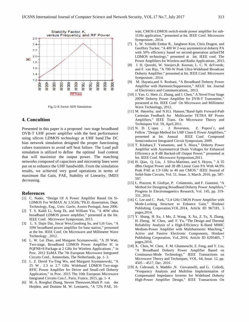
For unconditional stability: K > 1 and |△|< 1.
Figure.12. shows K factor and the necessary condition of stability of amplifier at 400-900MHz. in ADS simulation.
IJCSNS International Journal of Computer Science and Network Security, VOL.17 No.7, July 2017 313
Fig.12 K Factor ADS Simulation.
4. Concultion
Presented in this paper is a proposed two stage broadband DVB-T UHF power amplifier with the best performance using silicon LDMOS technology at UHF band.The DC bias network simulation designed the proper functioning values transistors to avoid self heat failure. The Load pull simulation is utilized to define the optimal load content that will maximize the output power. The matching networks composed of capacitors and microstrip lines were put on to enhance the UHF bandwidth. From the simulation results, we achieved very good operations in terms of maximum flat Gain, PAE, Stability of Linearity, IMD3 decreasing.
References [1] C. Nader, “Design Of A Power Amplifier Based On Si-
LDMOS For WiMAX At 3.5GHz,”Ph.D. dissertation, Dept. Technology, Eng., Univ. Gavle, Aveiro Portugal, June 2006.
[2] T. S. Kaldi Li, Song Di, and William Yin, “A 40W ultra broadband LDMOS power amplifier,” presented at the Int. IEEE Conf. Microwave Symposium, 2015.
[3] L. S. Dajie Dai, Jincai Wen,Guodong Su, and Lili Guo, “A 10W broadband power amplifier for base station,” presented at the Int. IEEE Conf. On Microwave and Millimeter Wave Technology , 2012.
[4] L. W. Lei Zhao, and Margaret Szymanowski, “A 20 Watt, Two-stage, Broadband LDMOS Power Amplifier IC in PQFN8×8 Package at 2 GHz for Wireless Applications ,” in Proc. 2012 EuMA The 7th European Microwave Integrated Circuits Conf., Amsterdam, The Netherlands, pp. 1- 3.
[5] L. Z. David Yu-Ting Wu, and Margaret Szymanowski, “A 25 W , 2.3 to 2.7 GHz Wideband LDMOS Two-stage RFIC Power Amplifier for Driver and Small-cell Doherty Application,” in Proc. 2015 The 10th European Microwave Integrated Circuits Con.f., Paris, France, 2015, pp. 1- 4.
[6] M. A. Ronghui Zhang, Steven Theeuwen,Mark P. van der Heijden, and Domine M. W. Leenaerts, “A 72% PAE, 10-
watt, CMOS-LDMOS switch-mode power amplifier for sub-1GHz application,” presented at Int. IEEE Conf. Microwave Symposium , 2014.
[7] L. W. Srinidhi Embar R., Jangheon Kim, Chris Dragon, and Geoffrey Tucker, “A 400 W 2-way asymmetrical doherty PA with 50% efficiency based on second-generation airfastTM LDMOS technology,” presented at Int. IEEE conf. The Power Amplifiers for Wireless and Radio Applications , 2015.
[8] J. H. Qureshi, W. Sneijers,R. Keenan, L. C. N. deVreede, and F. van Rijs, “A 700-W Peak Ultra-Wideband Broadcast Doherty Amplifier,” presented at Int. IEEE Conf. Microwave Symposium , 2014.
[9] M. Hayatia,and S. Roshani, “A Broadband Doherty Power Amplifier with HarmonicSuppression,” AEUE Int. Journal of Electronics and Communications,. 2013.
[10] J. Yao, G. Shen ,G. Zhang, and J. Chen,” A Novel Four Stage 200W Doherty Power Amplifier for DVB-T Transmitter,” presented at Int. IEEE Conf On Microwave and Millimeter Wave Technology, 2012.
[11] M. Høyerby, and N.H.L Hansen,”Band-Split Forward-Path Cartesian Feedback for Multicarrier TETRA RF Power Amplifiers,” IEEE Trans. On Microwave Theory and Techniques Vol. 59, April.2011.
[12] N. D. L´opez , J. Hoversten, Z. Popovi´c, and Fellow ,”Design Method for UHF Class-E Power Amplifiers,” presented at Int. Annual IEEE Conf. Compound Semiconductor Integrated Circuit Symposium, 2009.
[13] T. Kitahara,T. Yamamoto, and S. Hiura,” Doherty Power Amplifier with Asymmetrical Drain Voltages for Enhanced Efficiency at 8 dB Backed-off Output Power,” presented at Int. IEEE Conf. Microwave Symposium,2011.
[14] H. Qian, Q. Liu, J. Silva-Martinez, and S. Hoyos, ” A 35 dBm Output Power and 38 dB Linear Gain PA With 44.9% Peak PAE at 1.9 GHz in 40 nm CMOS.” IEEE Journal of Solid-State Circuits, Vol. 51, Issue. 3, March .2016. pp. 587-597.
[15] L. Piazzon, R. Giofrµe, P. Colantonio, and F. Giannini, “A Method for Designing Broadband Doherty Power Amplifers,” Progress In Electromagnetics Research, Vol. 145, pp. 319-331, 2014.
[16] C. Lee and C. Park, “2.4 GHz CMOS Power Amplifier with Mode-Locking Structure to Enhance Gain,” Hindawi Publishing Corporation,VOL.2014, Article ID 967181, 5 pages,2014.
[17] Y. Shang, H. Xu, J. Mo, Z. Wang, X. Xu, Z. Tu, X. Zhang, H. Zheng, W. Chen, and F. Yu, “The Design and Thermal Reliability Analysis of a High-Efficiency K-Band MMIC Medium-Power Amplifier with Multiharmonic Matching,” Active and Passive Electronic Components, Hindawi Publishing Corporation, VoL.2016, Article ID 6295405, 7 pages,2016.
[18] X. Chen, W. Chen, F. M. Ghannouchi, Z. Feng, and Y. Liu, “A Broadband Doherty Power Amplifier Based on Continuous-Mode Technology,” IEEE Transactions on Microwave Theory and Techniques, VOL. 64, Issue. 12, pp. 4505 – 4517, Dec. 2016 .
[19] A. Cidronali, S. Maddio ,N. Giovannelli, and G. Collodi, “Frequency Analysis and Multiline Implementation of Compensated Impedance Inverter for Wideband Doherty High-Power Amplifier Design,” IEEE Transactions On
IJCSNS International Journal of Computer Science and Network Security, VOL.17 No.7, July 2017 314
Microwave THEORY AND TECHNIQUES, VOL. 64, NO. 5, MAY 2016.
[20] Y. Dong, L. Mao and S. Xie, “Fully Integrated Class-J Power Amplifier in Standard CMOS Technology,” IEEE Microwave and Wireless Components Letters Vol.27, Issue. 1, Jan. 2017.
[21] W. Hallberg, M. Özen, D. Gustafsson,K. Buisman, and C. Fager, “A Doherty Power Amplifier Design Method for Improved Efficiency and Linearity,” IEEE Transactions on Microwave Theory and Techniques Vol.64, Issue.12, Dec. 2016.
[22] J. Hur, H. Kim, O. Lee, K. W. Kim, K. Lim, C. Lee and J. Laskar, “A Multi-Level Class D CMOS Power Amplifier for an Out-Phasing Transmitter with a Non-Isolated Power Combiner,” IEEE Transactions on Circuits and Systems II: Express Briefs Vol.63, Issue. 7, July 2016 .
[23] W. Jang, R. Cordeiro, G. Arnaldo Oliveira, and N. B. Carvalho, “A Broadband Almost-Digital RF Transmitter With an Efficient Power Amplifier,” IEEE Transactions on Microwave Theory and Techniques, Vol.64, Issue. 5, May 2016.
[24] K. Kim, J. Ko, S. Lee, and S. Nam, “A Two-Stage Broadband Fully Integrated CMOS Linear Power Amplifier for LTE Applications,” IEEE Transactions on Circuits and Systems II: Express Briefs ,Vol.63, Issue. 6, June 2016 .
[25] H. Lee, and et al., “Optimized Current of the Peaking Amplifier for Two-Stage Doherty Power Amplifier,” IEEE Transactions on Microwave Theory and Techniques Vol. 65, Issue.1, Jan. 2017.
[26] M. Özen,K. Andersson, and C.Fager, “Symmetrical Doherty Power Amplifier With Extended Efficiency Range,” IEEE Transactions on Microwave Theory and Techniques Vol. 64, Issue. 4, April 2016.
[27] J. Pang and et al., “Design of continuous-mode GaN power amplifier with compact fundamental impedance solutions on package plane,” IET Microwaves, Antennas & Propagation Vol. 10, Issue. 10, 7 18 2016.
[28] T. Qi, S. He and W. Shi , “Third-octave power amplifier using ring based matching network with high efficiency.” ELECTRONICS LETTERS ,Vol. 52 , No. 10 pp. 883–885, 12th May 2016.
[29] H. Taghavi and et.al., “Sequential Load-pull Technique for Multi-octave Design of RF Power Amplifiers,” IEEE Transactions on Circuits and Systems II: Express Briefs Vol. 63, Issue.9, Sept. 2016.
[30] H.F. Wu and et al. , “Analysis and Design of an Ultrabroadband Stacked Power Amplifier in CMOS Technology,” IEEE Transactions on Circuits and Systems II: Express Briefs Vol. 63, Issue. 1, Jan. 2016.
[31] J. Yi, Y. Yang, M. Park, W. Kang, and B. Kim,” Analog Predistortion Linearizer for High-Power RF Amplifiers,” IEEE Trans. On Microwave Theory and Techniques Vol. 48, Dec. 2000.
[32] P. Banelli, G. Baruffa, and S. Cacopardi,” Effects of HPA Non Linearity on Frequency Multiplexed OFDM Signals,” IEEE Trans. On Broadcasting, Vol. 47, No. 2, June. 2001.
[33] C. Sun, T. Liu, Y. Ye, Y. Zhang, X. Luo,and H. Lin,”Asymmetrical Doherty Power Amplifiers for LTEAdvancedSystems,”presented at Int. IEEE Conf. Microwave and Millimeter Wave Technology, 2012.
[34] D. Fan, Y. Deng, and Z n.. Li,”Design and Simulation of a Wideband PowerAmplifier from 600MHz to 1000MHz,”presented at the 3rd Int. IEEE Conf. Symposium on Microwave Antenna Propagation and EMC Technologies for Wireless Communications, 2009.
[35] H. J. Zhou,and H. F. Wu,” Design Of An S-Band Two-Way Inverted Asym-Metrical Doherty Power,” Progress In Electromagnetics Research Letters,Vol. 39 ,2013.
[36] C. Sun, T. Liu, Y. Ye, Y. Zhao, X. Luo,and J. Li,” Optimization Design of A Broadband Three-Stage Doherty Power Amplifier,” presented at Int. IEEE Conf. On Electronics, Communications and Control ,2011.
[37] D. Y. T. Wu, J. Annes, M. Bokatius,P. Hart,E. Krvavac,and G. Tucker,”A 350 W, 790 to 960 MHz Wideband LDMOS Doherty Amplifierusing a Modified Combining Scheme,”presented at Int. IEEE Conf. Microwave Symposium , 2014.
[38] S. J. C. H Theeuwen,and J. H. Qureshi, “LDMOS Technology for RF Power Amplifiers,” IEEE Trans. On Microwave Theory And Techniques, Vol. 60, 2012.
[39] A. C. N. Giovanneu, P. Singerl, S. Maddiol, C. Schuberth, and G. M. A. Del Chiaro, “A 250W LDMOS Doherty PA with 31% of Fractional Bandwidth forDVB-T Applications,” presented at Int. IEEE Conf. Microwave Symposium, 2014 .
[40] Y. Z. FuchengHou, “RF LDMOS Power Transistor for Multi-Carrier GSM Base Station,” presented at Int. IEEE Conf. Wireless Symposium ,2014.
[41] J. K. B. Kim, I. Kim, J. Cha, and S. Hong, “Microwave Doherty Power Amplifier for HighEfficiency and Linearity,” presented at Int. IEEE Conf. Workshop on Integrated Nonlinear Microwave and Millimeter Wave Circuits, 2006.
[42] S. S. B.V. Ramarao , J. K. Mishra , M. Pande , P. Singh , G. Kumar ,and J. Mukherjee, “Development of 3kW at 325MHz solid-state RF power amplifier usingfour power amplifier modules,” Science Direct Nuclear Instruments and Methods in Physics Research, 2014.
[43] D. H. Chuc,and B. G. Duong, “Design and fabrication of a high power S band LDMOS amplifier for microwave powertransmission and wireless communication,” Int. Journal of Advancements in Communication Technologies , vol. 1 , 2014.
[44] R. Ludwig, and P. Bretchko, RF CIRCUIT DESIGN:THEORY AND APPLICATIONS. Prentic Hall:Tom Robbins,2000.
[45] V. Prodanov, and M. Banu, “Power Amplifier Principles and Modern Design Techniques,” in Wireless Technologies Circuits, Systems, and Devices K. Iniewski, Ed.,2007, pp. 349-381.