design of an audio interface for patmos · 2017-01-26 · design of an audio interface for patmos...
TRANSCRIPT
Design of an Audio Interface for Patmos
02211 Advanced Computer Architecture
Daniel Sanz AusinDepartment of Applied Mathematics and
Computer ScienceTechnical University of [email protected]
Fabian GoergeDepartment of Applied Mathematics and
Computer ScienceTechnical University of [email protected]
ABSTRACTThis paper describes the design and implementation of anaudio interface for the Patmos processor, which runs on anAltera DE2-115 FPGA board. This board has an audio codecincluded, the WM8731. The interface described in this workallows to receive and send audio from and to the WM8731,and to synthesize, store or manipulate audio signals writingC programs for Patmos.
The structure of this project is integrated with the Patmosproject: new hardware modules have been added as IOs,which allow the communication between the processor andthe audio codec. These modules include a clock generatorfor the audio chip, ADC and DAC modules for the audioconversion from analog to digital and vice versa, and anI2C module which allows setting configuration parameterson the audio codec. Moreover, a top module has been cre-ated, which connects all the modules previously mentionedbetween them, to Patmos and to the WM8731, using the ex-ternal pins of the FPGA.
Simulations have been done using the Patmos emulator tocheck the correct functionality of all the modules. Afterthat, the Patmos processor with the audio interface has beensynthesized and loaded into the Altera FPGA. C programshave been written, and SignalTap, the logic analyzer fromQuartus, has been used to verify that the modules work asexpected.
The results show that the audio interface works as desired:the implemented C programs show that the audio is inputand output to and from Patmos correctly, with the rightformat and the expected sampling frequency. The analogueaudio signal output from the FPGA has been recorded usingan external audio interface, and the signals look exactly asanticipated.
1. INTRODUCTIONThe audio interface described in this paper is intended to beused with the Patmos processor. Patmos is an open sourceRISC ISAs with a load-store architecture, that is optimizedfor Real-Time Systems. Patmos is part of a project foundedby the European Union called T-CREST (Time-predictableMulti-Core Architecture for Embedded Systems).[5]
The majority of the hardware development for Patmos wasdone with the hardware description language Chisel. Chiselis an open-source Scala-based hardware description languagedeveloped by the university of Berkeley. [3] All the develop-ment in this project was also Chisel-based.
The development is based on the DE2-115 FPGA board fromAltera. Hence focuses this paper also on the communicationwith the on board WM8731 audio codec from Wolfson.
The paper is organized as follows: The following Section 2discusses the related work. Section 3 introduces the designof the audio interface. Section 4 covers the implementationsin Chisel, VHDL and C as well as the FPGA integrationprocess. After that Section 5 presents the evaluation andfinally, section 6 concludes the paper.
2. RELATED WORKAs mentioned before, this project has been developped us-ing Patmos, the open source real-time RISC processor de-velopped by T-CREST. There are many different versions ofthe Patmos processor, including a multi-core version with 9cores. But, for this project, the most simple 1-core versionhas been used.
Jose Albiach discusses in his master thesis the FPGA im-plementation for the WM8731 audio codec on an Altera UP3board. In his work he briefly summarizes the functionalityand then describes his approach to interact with the audiochip. In his work he suggest to divides the clock to generatethe needed clock signals for the audio chip. [1]
3. DESIGNIn the Altera data sheet for the DE2-115 Board the basic fea-tures and concept of the Wolfson WM8731 audio encoder anddecoder can be found. The WM8731 has line-in and line-outports as well as a microphone-in. The chip can be config-ured under use of the I2C bus to set parameters such asthe volume, the sampling frequency, and so on. The FPGApins connected to the audio chip are for input audio data
arX
iv:1
701.
0638
2v1
[cs
.AR
] 2
3 Ja
n 20
17
(ADCDAT) and output audio data (DACDAT) as well as thererespective sampling clocks (ADCLRCK, DACLRCK), which areused for synchronization. Furthermore a master clock inputfor the chip is available (XCK), and an additional clock usedfor the ADC and DAC (BCLK). Finally, there are two pins forthe I2C interface: data (SDAT) and clock (SCLK). [2, chapter4.11]
It was necessary to consult the data sheet of the WM8731
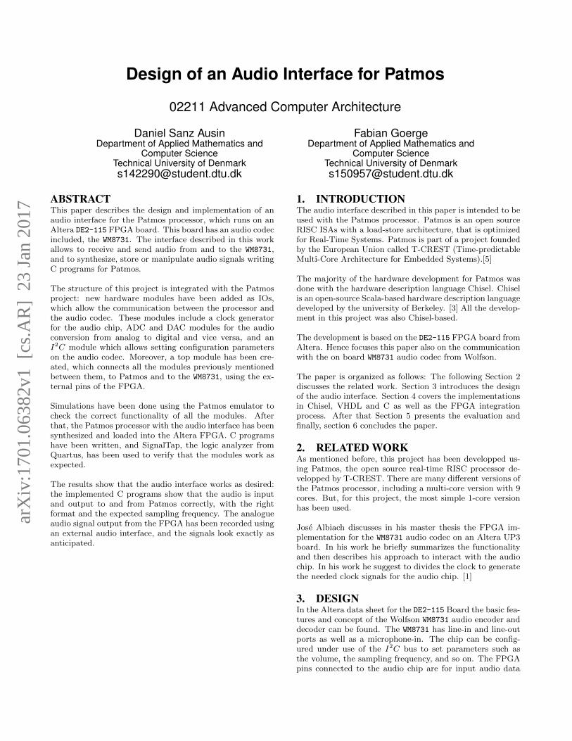
for a better understating. It can be clearly seen from therethat there are two main separated parts: the digital audiointerface and the control interface. [4] According to this,the design was split into smaller modules, in order to keepa good structure of the system. An overview of the designcan be seen in Figure 1. Patmos and the created audiointerface communicate via the open core protocol. Applica-tions on the Patmos processor can then write or read audiodata and configuration parameters to or from registers in theaudio interface. The ”AudioDAC” and ”AudioADC” compo-nents exchange the content of the audio registers with theaudio chip in the correct format for the audio interface ofthe WM8731. Likewise, the ”Audio I2C” component writesthe data and address of the configuration registers using theI2C protocol. For both the conversion from digital to ana-log and from analog to digital audio data, sampling clocksare needed. Therefore, the clock generation unit generatesthe master clock input (XCK) and the digital audio bit clock(BCLK). Later these units will be described in more detail.
Figure 1: Overview of the Design
3.1 Audio Interface ComponentThe audio interface is designed to be the heart of the imple-mentation which includes all the described components (seeFigure 1).
The audio interface has different registers in which Patmoscan write and read from. Depending on its functionality willsome registers only be readable.
Additionally, this component will specify the desired outputpins, which will be 1-bit outputs for the digital to analogdata (dacDat) and the sample rate clocks (dacLrc, adcLrc)and a 1-bit input for the analog to digital data (adcDat).The audio chip will be used in slave mode and will be clockedby the FPGA hence there are also pins needed for the masterclock (XCK) and the bit clock (BCLK). Moreover, does the I2Cinterface need two outputs (Data abd Clock). The datasignal is bidirectional (as it will be described in the next
subsection), so it needs both an input and output pin aswell as a write enable signal. This 3-state buffer design isused because it is impossible to define inout types in Chisel.
Furthermore, this unit forwards the default configurationsfrom the hardware configuration XML file to the submod-ules. The configuration parameters for the audio interfaceinclude the audio data length, which can be either 16, 20,24 or 32-bit, the sampling frequency (Fs) divider, which canrange from 8kHz to 96kHz, and finally the divider for theclock signals into the audio codec (BCLK and XCLK). For thislast signal the divider value chosen is 6, to get a frequency of13.33MHz into the audio codec from the 80MHz frequencyof Patmos.
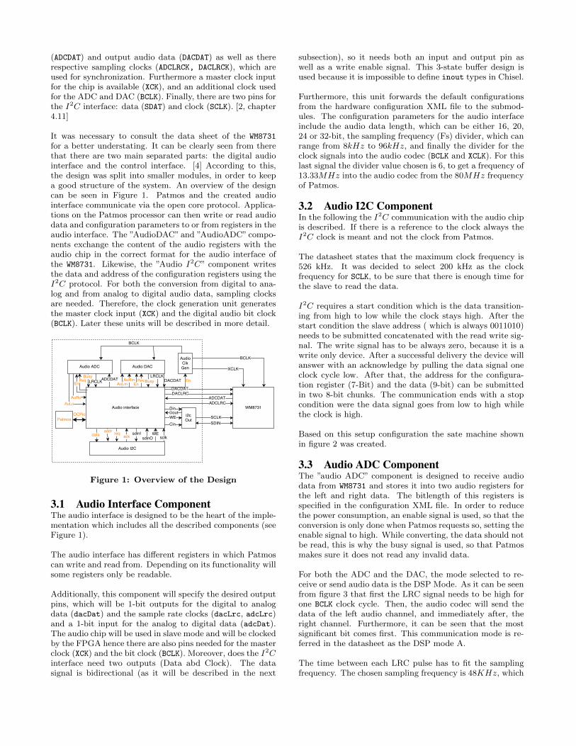
3.2 Audio I2C ComponentIn the following the I2C communication with the audio chipis described. If there is a reference to the clock always theI2C clock is meant and not the clock from Patmos.
The datasheet states that the maximum clock frequency is526 kHz. It was decided to select 200 kHz as the clockfrequency for SCLK, to be sure that there is enough time forthe slave to read the data.
I2C requires a start condition which is the data transition-ing from high to low while the clock stays high. After thestart condition the slave address ( which is always 0011010)needs to be submitted concatenated with the read write sig-nal. The write signal has to be always zero, because it is awrite only device. After a successful delivery the device willanswer with an acknowledge by pulling the data signal oneclock cycle low. After that, the address for the configura-tion register (7-Bit) and the data (9-bit) can be submittedin two 8-bit chunks. The communication ends with a stopcondition were the data signal goes from low to high whilethe clock is high.
Based on this setup configuration the sate machine shownin figure 2 was created.
3.3 Audio ADC ComponentThe ”audio ADC” component is designed to receive audiodata from WM8731 and stores it into two audio registers forthe left and right data. The bitlength of this registers isspecified in the configuration XML file. In order to reducethe power consumption, an enable signal is used, so that theconversion is only done when Patmos requests so, setting theenable signal to high. While converting, the data should notbe read, this is why the busy signal is used, so that Patmosmakes sure it does not read any invalid data.
For both the ADC and the DAC, the mode selected to re-ceive or send audio data is the DSP Mode. As it can be seenfrom figure 3 that first the LRC signal needs to be high forone BCLK clock cycle. Then, the audio codec will send thedata of the left audio channel, and immediately after, theright channel. Furthermore, it can be seen that the mostsignificant bit comes first. This communication mode is re-ferred in the datasheet as the DSP mode A.
The time between each LRC pulse has to fit the samplingfrequency. The chosen sampling frequency is 48KHz, which
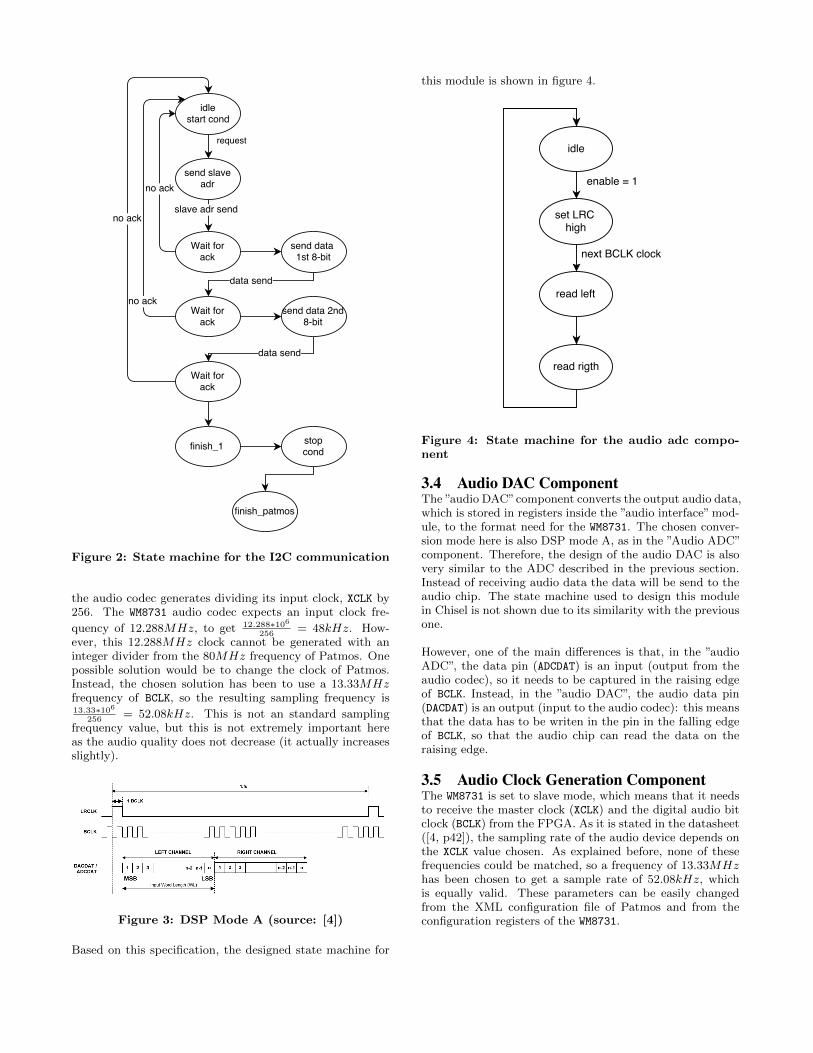
Figure 2: State machine for the I2C communication
the audio codec generates dividing its input clock, XCLK by256. The WM8731 audio codec expects an input clock fre-
quency of 12.288MHz, to get 12.288∗106256
= 48kHz. How-ever, this 12.288MHz clock cannot be generated with aninteger divider from the 80MHz frequency of Patmos. Onepossible solution would be to change the clock of Patmos.Instead, the chosen solution has been to use a 13.33MHzfrequency of BCLK, so the resulting sampling frequency is13.33∗106
256= 52.08kHz. This is not an standard sampling
frequency value, but this is not extremely important hereas the audio quality does not decrease (it actually increasesslightly).
Figure 3: DSP Mode A (source: [4])
Based on this specification, the designed state machine for
this module is shown in figure 4.
Figure 4: State machine for the audio adc compo-nent
3.4 Audio DAC ComponentThe ”audio DAC”component converts the output audio data,which is stored in registers inside the ”audio interface” mod-ule, to the format need for the WM8731. The chosen conver-sion mode here is also DSP mode A, as in the ”Audio ADC”component. Therefore, the design of the audio DAC is alsovery similar to the ADC described in the previous section.Instead of receiving audio data the data will be send to theaudio chip. The state machine used to design this modulein Chisel is not shown due to its similarity with the previousone.
However, one of the main differences is that, in the ”audioADC”, the data pin (ADCDAT) is an input (output from theaudio codec), so it needs to be captured in the raising edgeof BCLK. Instead, in the ”audio DAC”, the audio data pin(DACDAT) is an output (input to the audio codec): this meansthat the data has to be writen in the pin in the falling edgeof BCLK, so that the audio chip can read the data on theraising edge.
3.5 Audio Clock Generation ComponentThe WM8731 is set to slave mode, which means that it needsto receive the master clock (XCLK) and the digital audio bitclock (BCLK) from the FPGA. As it is stated in the datasheet([4, p42]), the sampling rate of the audio device depends onthe XCLK value chosen. As explained before, none of thesefrequencies could be matched, so a frequency of 13.33MHzhas been chosen to get a sample rate of 52.08kHz, whichis equally valid. These parameters can be easily changedfrom the XML configuration file of Patmos and from theconfiguration registers of the WM8731.
4. IMPLEMENTATIONThis section briefly describes the implementation of the de-sign in the Altera DE2-115 board, and points out challengesand methods used to achieve a successful implementation.All the files are publicly available at:
https://github.com/dsanz006/audio_patmos.git
4.1 I2C and ADC ImplementationThe first goal was to get a minimal working solution andthen extend the working design. For a minimal working so-lution it was both required to configure the registers andwrite something on the ADC channel. Initially, in order toverify that the modules mentioned before were implementedcorrectly, the Patmos emulator was used. Figure 5 shows theI2C waveform graph. It can be seen that first interface ad-dress (0011010) plus the concatenate 0 are transmitted andthen the address and data signals. Also the clock length isverified. After one 8-bit data is sent the we signal is set tolow to let the audio codec pull sdata down as an acknowl-edge.
Figure 5: Simulation of the I2C communication
In figure 6, the simulation of DAC communication is shown.It can be seen that the LRC signal comes first, and then theleft and right channel are transmitted.
Figure 6: Simulation of the DAC communication
4.2 SignalTapOne of the main difficulties during the synthesis on theFPGA was that the configuration registers of the WM8731 areread only: this means that it is not possible to check if datawas written on them correctly. With the help of the logicanalyzer, SignalTap, that Quartus provides it was possibleto get a better insight into what was happening. Lookingat the waveforms from SingalTap helped immensely becauseit included the response of the audio chip. As it can beseen in figure 7 the acknowledge signal comes as desired af-ter every eight bit submitted. This means that the data isbeing written into the configuration registers correctly. Thiscan also also verified by checking some of the configurationparameters, such as the volume.
Again, SignalTap was used to check that the audio data wasbeing sent and received correctly into and from the WM8731.
Figure 7: SignalTap capture of the I2C communica-tion
Looking at the digital audio signals it could be verified thatthe format corresponds to DSP mode A, as expected. Thisis shown in figure 8.
Figure 8: SignalTap capture of the audio DAC com-munication in detail
In figure 9 a submission of two consecutive audio packetscan be seen. The LRCK signals are 1536 cycles apart. Witha clock period of 80MHz, this corresponds to a period of19.2µs ( 1536
80∗106 ). So the frequency is 119.2∗10−6 = 52.08kHz.
The logic analyzer was also used here to make the signalslook exactly as it is specified in the datasheet.
Figure 9: SignalTap capture of the audio DAC com-munication overview
4.3 C ImplementationAll the work done, using the Chisel hardware descriptionlanguage, is intended to make it easier to write programs tomanipulate audio in many ways: recording and processingof a signal, synthesis, audio effects, and so on. It is muchmore suitable to write audio processing programs in a pro-gramming language such as C, and then run them on thePatmos processor instead of describing them in hardware.
The C programs developed include the library (audio.c),where some functions can be found to set up the configura-tion registers, write and read audio to and from the audiocodec and synchronise the audio signals. Several test pro-grams have been written which verify that this functionswork correctly. In a header file (audio.h) all the neededaddresses for the available registers are defined.
The two most important functions implemented are the onesthat read and write audio data from and to the WM8731. Asa design decision, it was chosen not to create any audiobuffer: this decision was chosen because Patmos is intendedto be a real-time processor, and audio buffers introduce adelay from input to output, which can lead to a loss of thereal-time concept. Instead, it has been decided that eachaudio sample is input, processed and output directly, witha delay of only 1 sample: 19.2µs. The way the audio inputand output function works is very simple: data is simplywritten or read to or from the audio data registers in theaudio interface (between Patmos and the WM8731). Then,
the hardware module takes care of transmitting this signalto the WM8731 only when the device is not busy, so whenthere is no conversion going on.
Additionally, it is necessary to synchronize each audio sam-ple with the sampling frequency, to avoid overwriting thesame values of data. Therefore, two synchronisation func-tions (for ADC and DAC) were created, which synchronizewith the sampling frequency by waiting for the LRC pulse.
Finally, there is a function available to change the volumeof the audio output. The volume can be set between +6and -73 db. No functions have been implemented for otherconfiguration registers, because the only parameter that isusually modified many times during execution is the volume.
4.4 FPGA TestsA simple test created to validate the implementation is aprogram to output a sine wave. While this test was running,the analog output was recorded using an external audio in-terface, and it could be confirmed that the output lookedexactly like a sinusoidal signal.
The second test was to output the data directly from theinput, without modifying it. This was done using a pro-gram where the data from the input registers was copied intothe output registers, and then waiting to the synchroniza-tion signal again. This program proved to work correctly:a drum machine was used to generate a drum loop audiosignal, and it was recorded directly using the external audiointerface. After that, the same audio signal was recordedagain, but this time going into and out of the FPGA: bothsignals looked exactly the same, and also sounded the same.
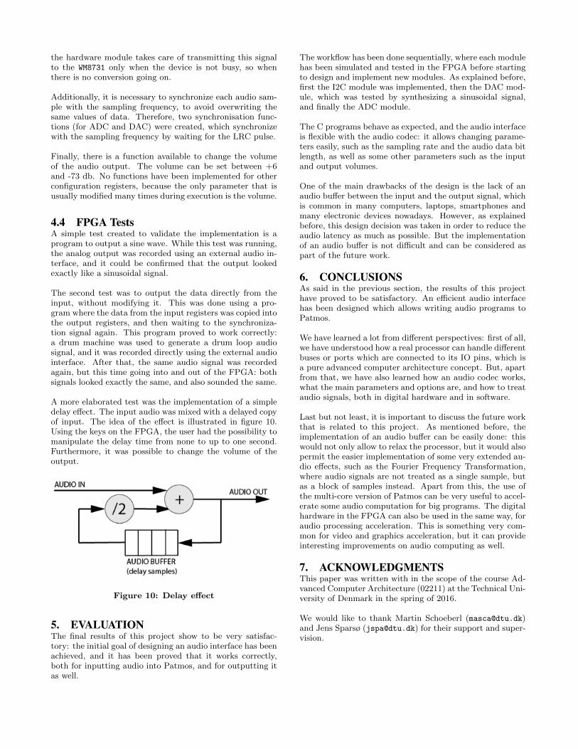
A more elaborated test was the implementation of a simpledelay effect. The input audio was mixed with a delayed copyof input. The idea of the effect is illustrated in figure 10.Using the keys on the FPGA, the user had the possibility tomanipulate the delay time from none to up to one second.Furthermore, it was possible to change the volume of theoutput.
Figure 10: Delay effect
5. EVALUATIONThe final results of this project show to be very satisfac-tory: the initial goal of designing an audio interface has beenachieved, and it has been proved that it works correctly,both for inputting audio into Patmos, and for outputting itas well.
The workflow has been done sequentially, where each modulehas been simulated and tested in the FPGA before startingto design and implement new modules. As explained before,first the I2C module was implemented, then the DAC mod-ule, which was tested by synthesizing a sinusoidal signal,and finally the ADC module.
The C programs behave as expected, and the audio interfaceis flexible with the audio codec: it allows changing parame-ters easily, such as the sampling rate and the audio data bitlength, as well as some other parameters such as the inputand output volumes.
One of the main drawbacks of the design is the lack of anaudio buffer between the input and the output signal, whichis common in many computers, laptops, smartphones andmany electronic devices nowadays. However, as explainedbefore, this design decision was taken in order to reduce theaudio latency as much as possible. But the implementationof an audio buffer is not difficult and can be considered aspart of the future work.
6. CONCLUSIONSAs said in the previous section, the results of this projecthave proved to be satisfactory. An efficient audio interfacehas been designed which allows writing audio programs toPatmos.
We have learned a lot from different perspectives: first of all,we have understood how a real processor can handle differentbuses or ports which are connected to its IO pins, which isa pure advanced computer architecture concept. But, apartfrom that, we have also learned how an audio codec works,what the main parameters and options are, and how to treataudio signals, both in digital hardware and in software.
Last but not least, it is important to discuss the future workthat is related to this project. As mentioned before, theimplementation of an audio buffer can be easily done: thiswould not only allow to relax the processor, but it would alsopermit the easier implementation of some very extended au-dio effects, such as the Fourier Frequency Transformation,where audio signals are not treated as a single sample, butas a block of samples instead. Apart from this, the use ofthe multi-core version of Patmos can be very useful to accel-erate some audio computation for big programs. The digitalhardware in the FPGA can also be used in the same way, foraudio processing acceleration. This is something very com-mon for video and graphics acceleration, but it can provideinteresting improvements on audio computing as well.
7. ACKNOWLEDGMENTSThis paper was written with in the scope of the course Ad-vanced Computer Architecture (02211) at the Technical Uni-versity of Denmark in the spring of 2016.
We would like to thank Martin Schoeberl ([email protected])and Jens Sparsø ([email protected]) for their support and super-vision.
8. REFERENCES[1] J. I. M. Albiach. Interfacing a processor core in fpga to
an audio system. Master’s thesis, Linkoping University,2006.
[2] Altera. De2-115 user manual.ftp://ftp.altera.com/up/pub/Altera_Material/
Boards/DE2-115/DE2_115_User_Manual.pdf. Date:2016-04-19.
[3] J. Bachrach, K. Asanovic, and J. Wawrzynek. Chisel2.2 tutorial. Technical report, EECS Department, UCBerkeley, July 2015.
[4] W. Microelectronics. Wm8731 - portable internet audiocodec with headphone driver and programmable samplerates. http://www.cirrus.com/en/pubs/proDatasheet/WM8731_v4.9.pdf. Date: 2016-04-19.
[5] M. Schoeberl, F. Brandner, S. Hepp, W. Puffitsch, andD. Prokesche. Patmos reference handbook. Technicalreport, DTU Compute, Technical University ofDenmark, October 2015.