design of an all-sic parallel dc/dc weinberg converter unit using
TRANSCRIPT

IEEE TRANSACTIONS ON POWER ELECTRONICS, VOL. 23, NO. 6, NOVEMBER 2008 2893
Design of an All-SiC Parallel DC/DC WeinbergConverter Unit Using RF Control
Sudip K. Mazumder, Senior Member, IEEE, Kaustuva Acharya, Student Member, IEEE,and Chuen Ming Tan, Member, IEEE
Abstract—We demonstrate the feasibility of RF communication-based wireless load-sharing control of a spatially distributed two-module parallel dc/dc (Weinberg) converter unit (DDCU), eachoperating at a high switching frequency (0.25 MHz) and deliv-ering an output power of 500 W. From control standpoint, wedemonstrate the feasibility of wireless control scheme using a dig-ital signal processing-field-programmable gate array (DSP-FPGAbased) control–communication interface. Further, using a com-posite Lyapunov function methodology, we determine (in the pres-ence of delay owing to channel disruption) the reachability of theDDCU under startup condition, and also investigate the effect ofdelay on orbital stability and performance. With regard to thehard-switched DDCU, we outline some practical design aspects ofthe high-frequency all-SiC Weinberg converter power stage andsubsequently demonstrate experimentally that the DDCU achieveshigh efficiency in spite of operating at high frequency and hightemperature, and exhibits satisfactory steady-state and transientperformances despite channel separation of up to 30 ft.
Index Terms—Control, dc/dc converter unit (DDCU), interna-tional space station (ISS), load sharing, network, power manage-ment and distribution unit design (PMAD), RF, reachability, SiC,stability, time delay, Weinberg converter, wireless.
I. INTRODUCTION
ONE OF THE important building blocks of National Aero-nautics and Space Administration (NASA’s) power man-
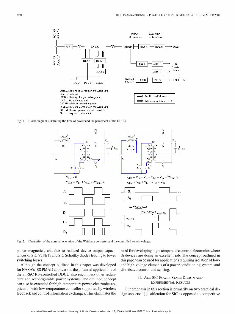
agement and distribution unit design (PMAD) for poweringthe international space station (ISS) is the dc/dc converter unit(DDCU), as illustrated in Fig. 1 [1]. Such a DDCU needs to haveparallel architecture for power scaling and system redundancy.Traditional approach to the control design of a parallel DDCUis based on decentralized droop methods [2] that offer highredundancy but at the price of often inadequate dynamic perfor-mance, or active-current-sharing methods [3] that overcome thelimitations of droop methods by ensuring even distribution of
Manuscript received December 4, 2007; revised March 8, 2008 and June 7,2008. Current version published December 9, 2008. Recommended for publica-tion by Associate Editor D. Maksimovic. This paper was presented at the IEEEPower Electronics Specialists Conference, Orlando, FL, June 2007. It was firstpublished in the proceedings of the same conference with the following details:S. K. Mazumder, C. Tan, and K. Acharya, “Design of a radio frequency con-trolled parallel dc-dc all-SiC converter,” IEEE Power Electronics SpecialistsConference, Orlando, Florida, pp. 2833–2839, Jun. 2007.
S. K. Mazumder and K. Acharya are with the Laboratory for Energyand Switching-Electronics Systems, Department of Electrical and Com-puter Engineering, University of Illinois, Chicago, IL 60607 USA (e-mail:[email protected]; [email protected]).
C. M. Tan is with the Linear Technology Corporation, Milpitas, CA 95035-7417 USA (e-mail: [email protected]).
Color versions of one or more of the figures in this paper are available onlineat http://ieeexplore.org.
Digital Object Identifier 10.1109/TPEL.2008.2004876
currents and stresses among the modules at the price of increas-ing physical connections with progressively higher number ofload-sharing modules.
To eliminate this problem associated with increased multi-plicity of physical connections, recently, the feasibility of RF-based “analog” wireless control of low-frequency (20 kHz)load-sharing dc/dc buck converters was demonstrated in [4]–[7],which achieves a satisfactory compromise between conventionaldroop and active-current-sharing control schemes. However,for very high-frequency operation, analog implementation cansuffer from drift problem that leads to pulsewidth modulation(PWM) dithering at the output of the receiver module. Further,the analog RF implementation in [7] (developed for dc/dc non-isolated buck converter) requires specific design for addressingthe limitation of the wireless transmitter with regard to trans-mitting low-bandwidth control signal.
This paper outlines a DSP-FPGA-based “fully digital” wire-less communication scheme for a two-module isolated Wein-berg DDCU operating at one order higher switching frequency(i.e., 0.25 MHz). To analyze the effect of delay due to channeldisruption at such high frequency under transient and steady-state conditions, we outline a robust analysis using compositeLyapunov-function-based methodology for reachability and or-bital stability analyses. We conduct a delay analysis to ascer-tain the impact of reduced-rate (delayed) data transmission andchannel disruption on the stability and performance of the load-sharing converter. We also demonstrate the feasibility of theparallel-converter control under such extreme conditions evenat distances of 30-ft separation between the converter modules.
Further, the Weinberg DDCU module (as illustrated in Fig. 2)for ISS was developed using radiation-hardened and high-temperature SiC verticle junction FET (VJFET) and SchottkySiC diodes because harsh conditions can be detrimental to Sipower devices [8]–[12]. Since there is no prior work on all-SiCWeinberg converter design, we outline the design of the SiCconverter (with following parameters: input voltage = 117–173 V, output voltage = 125 V, and output power = 1 kW), andexperimentally test the operation of the SiC devices at case tem-peratures up to 200 ◦C. A maximum experimental efficiency ofmore than 91% is obtained at the low line even at 0.25 MHz (forhard-switched operation) and for high case temperature. Thisis achieved by eliminating lossy snubbers [11] (because unlikeSi devices, SiC devices can sustain higher breakdown voltagewithout compromising switch transfer efficiency [14]–[18]), re-ducing leakage inductances of the coupled inductor and thecenter-tapped transformer (that reduce the voltage spike and theassociated device switching losses) by using suitably designed
0885-8993/$25.00 © 2008 IEEE
Authorized licensed use limited to: University of Illinois. Downloaded on March 7, 2009 at 14:57 from IEEE Xplore. Restrictions apply.
2894 IEEE TRANSACTIONS ON POWER ELECTRONICS, VOL. 23, NO. 6, NOVEMBER 2008
Fig. 1. Block diagram illustrating the flow of power and the placement of the DDCU.
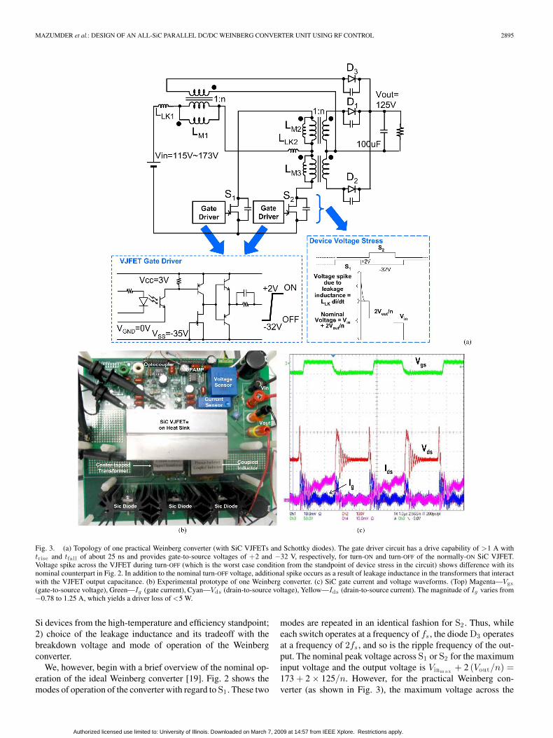
Fig. 2. Illustration of the nominal operation of the Weinberg converter and the controlled switch voltage.
planar magnetics, and due to reduced device output capaci-tances of SiC VJFETs and SiC Schottky diodes leading to lowerswitching losses.
Although the concept outlined in this paper was developedfor NASA’s ISS PMAD application, the potential applications ofthe all-SiC RF-controlled DDCU also encompass other redun-dant and reconfigurable power systems. The outlined conceptcan also be extended for high-temperature power-electronics ap-plication with low-temperature controller supported by wirelessfeedback and control information exchanges. This eliminates the
need for developing high-temperature control electronics whereSi devices are doing an excellent job. The concept outlined inthis paper can be used for applications requiring isolation of low-and high-voltage elements of a power conditioning system, anddistributed control and sensing.
II. ALL-SiC POWER STAGE DESIGN AND
EXPERIMENTAL RESULTS
Our emphasis in this section is primarily on two practical de-sign aspects: 1) justification for SiC as opposed to competitive
Authorized licensed use limited to: University of Illinois. Downloaded on March 7, 2009 at 14:57 from IEEE Xplore. Restrictions apply.
MAZUMDER et al.: DESIGN OF AN ALL-SiC PARALLEL DC/DC WEINBERG CONVERTER UNIT USING RF CONTROL 2895
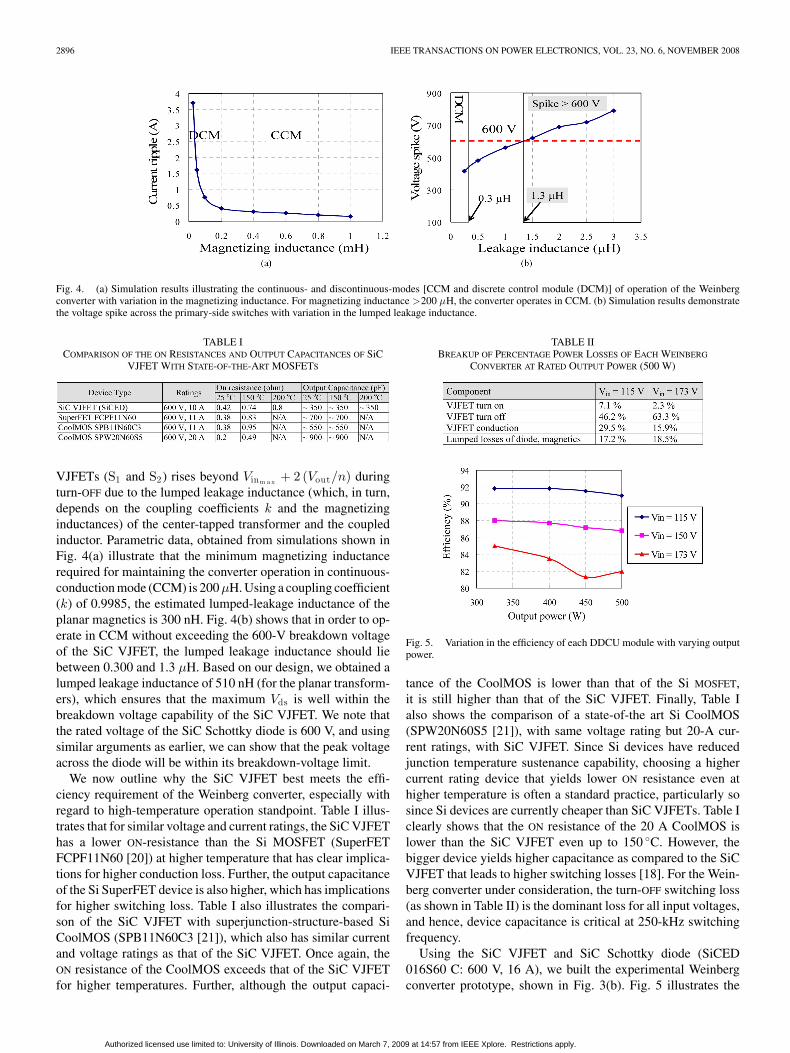
Fig. 3. (a) Topology of one practical Weinberg converter (with SiC VJFETs and Schottky diodes). The gate driver circuit has a drive capability of >1 A withtrise and tfa ll of about 25 ns and provides gate-to-source voltages of +2 and −32 V, respectively, for turn-ON and turn-OFF of the normally-ON SiC VJFET.Voltage spike across the VJFET during turn-OFF (which is the worst case condition from the standpoint of device stress in the circuit) shows difference with itsnominal counterpart in Fig. 2. In addition to the nominal turn-OFF voltage, additional spike occurs as a result of leakage inductance in the transformers that interactwith the VJFET output capacitance. (b) Experimental prototype of one Weinberg converter. (c) SiC gate current and voltage waveforms. (Top) Magenta—Vgs(gate-to-source voltage), Green—Ig (gate current), Cyan—Vds (drain-to-source voltage), Yellow—Ids (drain-to-source current). The magnitude of Ig varies from−0.78 to 1.25 A, which yields a driver loss of <5 W.
Si devices from the high-temperature and efficiency standpoint;2) choice of the leakage inductance and its tradeoff with thebreakdown voltage and mode of operation of the Weinbergconverter.
We, however, begin with a brief overview of the nominal op-eration of the ideal Weinberg converter [19]. Fig. 2 shows themodes of operation of the converter with regard to S1 . These two
modes are repeated in an identical fashion for S2 . Thus, whileeach switch operates at a frequency of fs , the diode D3 operatesat a frequency of 2fs , and so is the ripple frequency of the out-put. The nominal peak voltage across S1 or S2 for the maximuminput voltage and the output voltage is Vinm a x + 2 (Vout/n) =173 + 2 × 125/n. However, for the practical Weinberg con-verter (as shown in Fig. 3), the maximum voltage across the
Authorized licensed use limited to: University of Illinois. Downloaded on March 7, 2009 at 14:57 from IEEE Xplore. Restrictions apply.
2896 IEEE TRANSACTIONS ON POWER ELECTRONICS, VOL. 23, NO. 6, NOVEMBER 2008
Fig. 4. (a) Simulation results illustrating the continuous- and discontinuous-modes [CCM and discrete control module (DCM)] of operation of the Weinbergconverter with variation in the magnetizing inductance. For magnetizing inductance >200 µH, the converter operates in CCM. (b) Simulation results demonstratethe voltage spike across the primary-side switches with variation in the lumped leakage inductance.
TABLE ICOMPARISON OF THE ON RESISTANCES AND OUTPUT CAPACITANCES OF SiC
VJFET WITH STATE-OF-THE-ART MOSFETS
VJFETs (S1 and S2) rises beyond Vinm a x + 2 (Vout/n) duringturn-OFF due to the lumped leakage inductance (which, in turn,depends on the coupling coefficients k and the magnetizinginductances) of the center-tapped transformer and the coupledinductor. Parametric data, obtained from simulations shown inFig. 4(a) illustrate that the minimum magnetizing inductancerequired for maintaining the converter operation in continuous-conduction mode (CCM) is 200 µH. Using a coupling coefficient(k) of 0.9985, the estimated lumped-leakage inductance of theplanar magnetics is 300 nH. Fig. 4(b) shows that in order to op-erate in CCM without exceeding the 600-V breakdown voltageof the SiC VJFET, the lumped leakage inductance should liebetween 0.300 and 1.3 µH. Based on our design, we obtained alumped leakage inductance of 510 nH (for the planar transform-ers), which ensures that the maximum Vds is well within thebreakdown voltage capability of the SiC VJFET. We note thatthe rated voltage of the SiC Schottky diode is 600 V, and usingsimilar arguments as earlier, we can show that the peak voltageacross the diode will be within its breakdown-voltage limit.
We now outline why the SiC VJFET best meets the effi-ciency requirement of the Weinberg converter, especially withregard to high-temperature operation standpoint. Table I illus-trates that for similar voltage and current ratings, the SiC VJFEThas a lower ON-resistance than the Si MOSFET (SuperFETFCPF11N60 [20]) at higher temperature that has clear implica-tions for higher conduction loss. Further, the output capacitanceof the Si SuperFET device is also higher, which has implicationsfor higher switching loss. Table I also illustrates the compari-son of the SiC VJFET with superjunction-structure-based SiCoolMOS (SPB11N60C3 [21]), which also has similar currentand voltage ratings as that of the SiC VJFET. Once again, theON resistance of the CoolMOS exceeds that of the SiC VJFETfor higher temperatures. Further, although the output capaci-
TABLE IIBREAKUP OF PERCENTAGE POWER LOSSES OF EACH WEINBERG
CONVERTER AT RATED OUTPUT POWER (500 W)
Fig. 5. Variation in the efficiency of each DDCU module with varying outputpower.
tance of the CoolMOS is lower than that of the Si MOSFET,it is still higher than that of the SiC VJFET. Finally, Table Ialso shows the comparison of a state-of-the art Si CoolMOS(SPW20N60S5 [21]), with same voltage rating but 20-A cur-rent ratings, with SiC VJFET. Since Si devices have reducedjunction temperature sustenance capability, choosing a highercurrent rating device that yields lower ON resistance even athigher temperature is often a standard practice, particularly sosince Si devices are currently cheaper than SiC VJFETs. Table Iclearly shows that the ON resistance of the 20 A CoolMOS islower than the SiC VJFET even up to 150 ◦C. However, thebigger device yields higher capacitance as compared to the SiCVJFET that leads to higher switching losses [18]. For the Wein-berg converter under consideration, the turn-OFF switching loss(as shown in Table II) is the dominant loss for all input voltages,and hence, device capacitance is critical at 250-kHz switchingfrequency.
Using the SiC VJFET and SiC Schottky diode (SiCED016S60 C: 600 V, 16 A), we built the experimental Weinbergconverter prototype, shown in Fig. 3(b). Fig. 5 illustrates the
Authorized licensed use limited to: University of Illinois. Downloaded on March 7, 2009 at 14:57 from IEEE Xplore. Restrictions apply.

MAZUMDER et al.: DESIGN OF AN ALL-SiC PARALLEL DC/DC WEINBERG CONVERTER UNIT USING RF CONTROL 2897
Fig. 6. Progressively higher overlap of Vds and Ids during turn-OFF yields higher turn-OFF loss in the Weinberg converter.
Fig. 7. Variations. (a) ON resistance. (b) Output capacitance of the SiC VJFET. (c) SiC Schottky diode forward drop with increasing case temperature. To obtainthe result in (a), the SiC VJFETs are mounted on a heat sink that is placed on a hot plate to vary the case temperature. The SiC VJFETs are electrically connected tothe power stage printed circuit board (PCB). ON resistance is calculated by measuring the voltage drop across the drain and source terminals of the SiC VJFET asdrain-to-source current flows through it. Taking the ratio of the drain-to-source voltage drop and the drain-to-source current provides the ON resistance. To obtainthe result in (b), we place the device on a hot plate (to control the case temperature) and then connect the drain and the source to the impedance analyzer 4192 Afrom Agilent/HP. Subsequently, we apply a negative (−25 V) voltage between the gate and the source terminals of the SiC VJFET to turn it OFF. Finally, with thedevice turned OFF, the impedance analyzer determines output capacitance of the SiC VJFET. To obtain the result in (c), the SiC power diodes are mounted on theheatsink, which is placed on the hot plate to vary the case temperature of the diode. Differential probes are used to measure the forward drop of the SiC diode asthe case temperature is varied.
variation in the efficiency of each Weinberg converter mod-ule [Fig. 3(b)] with variation of the output power for three inputvoltage conditions. For Vin = 115 V and Vin = 173 V, the mea-sured efficiencies are 91.4% and 81.8%, respectively, at the ratedoperating power. Table II shows the breakup of power losses athigh- and low-input voltages. It shows that, more than half ofthe power loss is accrued by the switches during turn-OFF. Thisis because (and as illustrated in Fig. 6) during turn-OFF, Vdstransitions from 0 to Vds = Vin + 2Vout/n instead of 0 to Vin .Higher Vds along with higher Ids just before turn-OFF leads tohigher turn-OFF losses. The value of Ids just before turn-OFF ishigher when Vin = 173 V because the duty ratio reduces and theinductor current slope (Vin/LM ) increases. Therefore, the over-lap of Ids and Vds becomes even greater. Fig. 6 illustrates theprogressively higher overlap of Vds and Ids with increasing in-put voltage leading to higher turn-OFF loss. Finally, Fig. 7 showsthe impacts of increasing case temperature on the ON resistanceand output capacitance of the SiC VJFET and the forward dropof the SiC diode. It clearly demonstrates that with increasing
case temperatures, the switching losses of the VJFET and theconduction loss of the diode vary negligibly. The ON resistanceof the VJFET does increase by a factor of 2. Overall, the con-verter efficiency is expected to decrease by no more than 2% forthe worst case condition since the dominant loss is the turn-OFF
loss.
III. LOAD SHARING CONTROLLER DESIGN USING RFWIRELESS NETWORK
A. Controller Description
The load-sharing controller is implemented on a digital plat-form, as illustrated in Fig. 8 using a DSP (TI TMS320C6713),an FPGA (Altera Flex10 K), and a wireless transceiver(Microlinear ML2722). Such an implementation has severaladvantages, including 1) ease of implementation of complexcontrol schemes, 2) flexibility to realize different controllerstructures for different operating conditions, and 3) ability tomitigate effects of transceiver saturation, which is common in
Authorized licensed use limited to: University of Illinois. Downloaded on March 7, 2009 at 14:57 from IEEE Xplore. Restrictions apply.

2898 IEEE TRANSACTIONS ON POWER ELECTRONICS, VOL. 23, NO. 6, NOVEMBER 2008
Fig. 8. (a) Architecture of the digital controller. (b) Experimental hardware for implementing the digital controller.
analog transceivers and could distort the information exchangedamong the modules. We note here that at this stage, the digitalcontroller interface is designed to be flexible enough to al-low implementation of different control schemes and controlleralgorithms. However, eventually such a control–communicationinterface can and should be realized in a dedicated application-specific integrated circuit (ASIC) to reduce cost, board space,and debugging hurdles.
The overall digital controller architecture is illustrated inFig. 8(a). The load-sharing control scheme is implemented onthe DSPs of the two modules, while the PWM signal generationfor the converter switches and the voltage- and current-sensorinterfaces for each module are implemented on the FPGA. Forwireless communication, the protocol for medium access con-trol (MAC) layer [22] is implemented in the DSP while thetransmitter power control [22] is realized in the FPGA. The size
of the transmitted packet is 24 bits (for 12-bit control variablethat is exchanged among the modules). Finally, Fig. 8(b) illus-trates the hardware implementation, where all the key digitalcontroller blocks have been identified.
One of the problems with wireless control is packet drop thatresults in discontinuous communication between the master andslave, as illustrated in Fig. 9(a). The slave is out of synchroniza-tion and the master needs to support the additional current forthe time when the data is lost. It was observed that the data isdisrupted when the transmitter IC does a phase lock loop updateevery 100 ms. The disruption lasts for about 150 µs. Such a datacan have an adverse impact on the load sharing performanceof the parallel converters, as shown in Fig. 9(b). To overcomethis problem, a threshold level on the data received by the slavemodule is set. If the incoming data exceeds this threshold level,the data packet is discarded and the load-sharing data from the
Authorized licensed use limited to: University of Illinois. Downloaded on March 7, 2009 at 14:57 from IEEE Xplore. Restrictions apply.

MAZUMDER et al.: DESIGN OF AN ALL-SiC PARALLEL DC/DC WEINBERG CONVERTER UNIT USING RF CONTROL 2899
Fig. 9. (a) Discontinuous communication between the master and slave due to lack of synchronization. (b) Case when the received data is used by the slavecontroller without any changes leading to load-sharing error. (c) Case where data limiting ensures that the received data (before channel disruption) is used by theslave controller in case the current received data exceeds a threshold level. This yields satisfactory current sharing.
previous sample is used instead. Fig. 9(c) shows a much im-proved load sharing between the master and slave. However,this data-limiting scheme introduces an additional time delay inthe load-sharing information at the receiver apart from the delaydue to the transmission channel and due to processing of the datato be communicated at the transceiver and the receiver nodes.Therefore, in the next section, we study the impacts of timedelay on the stability and performance of the overall system.
B. Impacts of Time Delay on System Stability and Performance
In this section, we investigate the impacts of time delay on theglobal stability and performance of the system. Global stabilityanalyses involve determining the reaching conditions for orbitalexistence (which determines whether the error trajectories of thesystem converge to an orbit from an arbitrary initial condition)[23], [24] and the stability of the nominal (corresponding to theswitching period) steady state orbit [24], [25].
Fig. 10 illustrates the control block diagram of the Weinbergconverter. The state-space piecewise linear (PWL) model of theclosed-loop parallel Weinberg converter is described by
X = A0iX + A1iX (t − τD ) + Bi (1)
Fig. 10. Schematic illustrating the control block diagram of the load-sharingWeinberg converter [each module shown in Fig. 3(a)]. Symbol τD representsthe time delay due to RF communication between the two nodes.
Authorized licensed use limited to: University of Illinois. Downloaded on March 7, 2009 at 14:57 from IEEE Xplore. Restrictions apply.
2900 IEEE TRANSACTIONS ON POWER ELECTRONICS, VOL. 23, NO. 6, NOVEMBER 2008
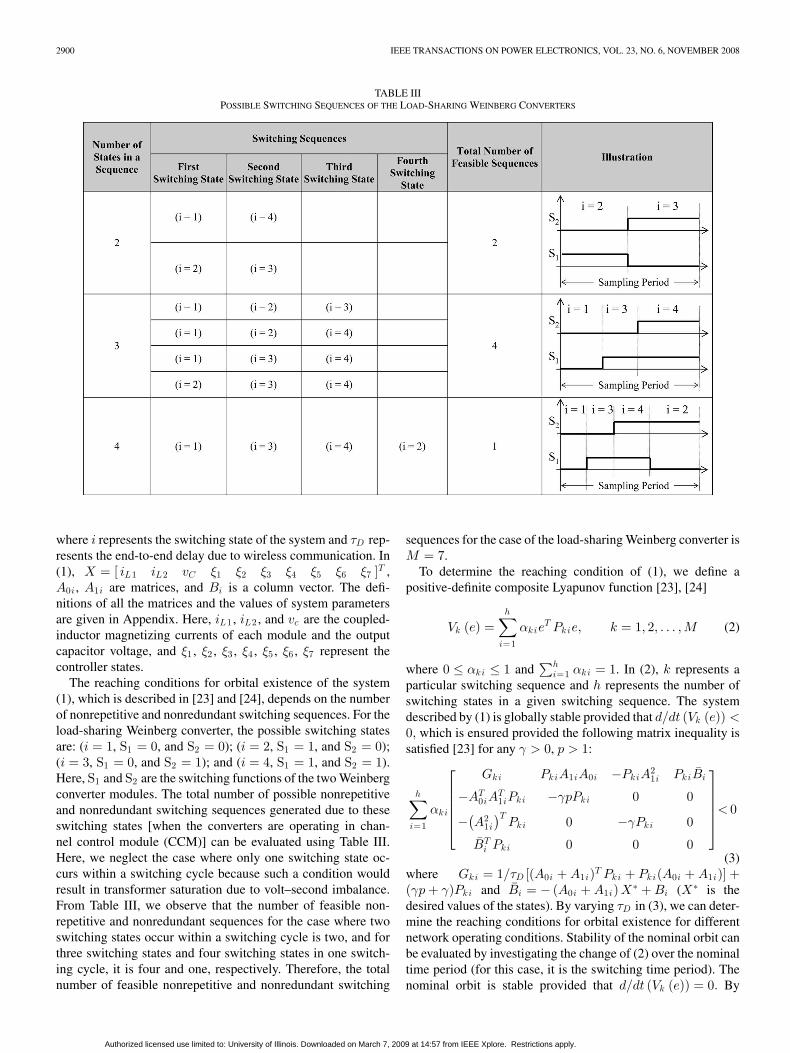
TABLE IIIPOSSIBLE SWITCHING SEQUENCES OF THE LOAD-SHARING WEINBERG CONVERTERS
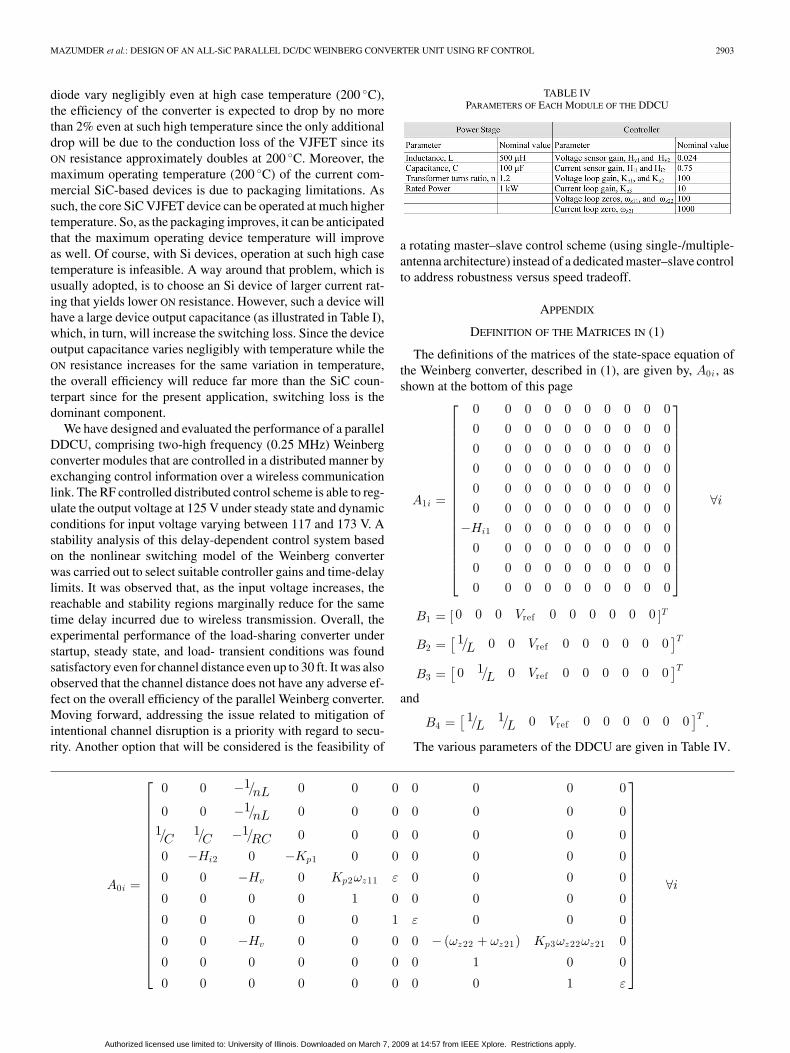
where i represents the switching state of the system and τD rep-resents the end-to-end delay due to wireless communication. In(1), X = [ iL1 iL2 vC ξ1 ξ2 ξ3 ξ4 ξ5 ξ6 ξ7 ]T ,A0i , A1i are matrices, and Bi is a column vector. The defi-nitions of all the matrices and the values of system parametersare given in Appendix. Here, iL1 , iL2 , and vc are the coupled-inductor magnetizing currents of each module and the outputcapacitor voltage, and ξ1 , ξ2 , ξ3 , ξ4 , ξ5 , ξ6 , ξ7 represent thecontroller states.
The reaching conditions for orbital existence of the system(1), which is described in [23] and [24], depends on the numberof nonrepetitive and nonredundant switching sequences. For theload-sharing Weinberg converter, the possible switching statesare: (i = 1, S1 = 0, and S2 = 0); (i = 2, S1 = 1, and S2 = 0);(i = 3, S1 = 0, and S2 = 1); and (i = 4, S1 = 1, and S2 = 1).Here, S1 and S2 are the switching functions of the two Weinbergconverter modules. The total number of possible nonrepetitiveand nonredundant switching sequences generated due to theseswitching states [when the converters are operating in chan-nel control module (CCM)] can be evaluated using Table III.Here, we neglect the case where only one switching state oc-curs within a switching cycle because such a condition wouldresult in transformer saturation due to volt–second imbalance.From Table III, we observe that the number of feasible non-repetitive and nonredundant sequences for the case where twoswitching states occur within a switching cycle is two, and forthree switching states and four switching states in one switch-ing cycle, it is four and one, respectively. Therefore, the totalnumber of feasible nonrepetitive and nonredundant switching
sequences for the case of the load-sharing Weinberg converter isM = 7.
To determine the reaching condition of (1), we define apositive-definite composite Lyapunov function [23], [24]
Vk (e) =h∑
i=1
αkieT Pkie, k = 1, 2, . . . ,M (2)
where 0 ≤ αki ≤ 1 and∑h
i=1 αki = 1. In (2), k represents aparticular switching sequence and h represents the number ofswitching states in a given switching sequence. The systemdescribed by (1) is globally stable provided that d/dt (Vk (e)) <0, which is ensured provided the following matrix inequality issatisfied [23] for any γ > 0, p > 1:
h∑i=1
αki
Gki PkiA1iA0i −PkiA21i PkiBi
−AT0iA
T1iPki −γpPki 0 0
−(A2
1i
)TPki 0 −γPki 0
BTi Pki 0 0 0
< 0
(3)where Gki = 1/τD [(A0i + A1i)T Pki + Pki(A0i + A1i)] +(γp + γ)Pki and Bi = − (A0i + A1i) X∗ + Bi (X∗ is thedesired values of the states). By varying τD in (3), we can deter-mine the reaching conditions for orbital existence for differentnetwork operating conditions. Stability of the nominal orbit canbe evaluated by investigating the change of (2) over the nominaltime period (for this case, it is the switching time period). Thenominal orbit is stable provided that d/dt (Vk (e)) = 0. By
Authorized licensed use limited to: University of Illinois. Downloaded on March 7, 2009 at 14:57 from IEEE Xplore. Restrictions apply.

MAZUMDER et al.: DESIGN OF AN ALL-SiC PARALLEL DC/DC WEINBERG CONVERTER UNIT USING RF CONTROL 2901
Fig. 11. (a) Variation of the maximum values of time delay that can be sus-tained by the system (1) while ensuring that the reaching condition for orbitalexistence is satisfied and the nominal steady state orbit is stable. (b) Variationof the maximum value of voltage loop gain that can be allowed for a given timedelay.
equating the left-hand side of (3) to zero, the condition forstability of the nominal orbit can be expressed as
h∑i=1
αki
Gki PkiA1iA0i −PkiA21i PkiBi
−AT0iA
T1iPki −γpPki 0 0
−(A2
1i
)TPki 0 −γPki 0
BTi Pki 0 0 0
= 0
(4)where Pki are positive-definite matrices and αki is obtainedusing the numerical search algorithm. If there are no positive-definite matrices Pki that satisfy (4), we conclude that the nom-inal orbit is unstable. We note that unlike the conventional map-based approach [25], which ascertains stability of (1) using amap that is derived by sequential patching of solutions corre-sponding to the ith state, and hence, requires the knowledgeof the modulation scheme, the composite Lyapunov-function-based approach depends only on the switching states of thenominal sequence. Even if the nominal sequence changes (e.g.,due to a change in the modulation scheme), (4) is true as longas the switching states in the sequence are the same.
Fig. 11(a) illustrates the maximum values of time delay thatcan be sustained by the system (while satisfying (3) and (4),respectively) for input voltage variation from 115 to 173 V.Clearly, higher time delays can be sustained by the system asthe input voltage reduces. The variation of the maximum allow-able voltage-loop gain (Kp1 and Kp2) with time delay is illus-trated in Fig. 11(b). For Fig. 11(b), the input voltage is 173 V.Fig. 11(a) and (b) can be used to design the controller param-
Fig. 12. Variation of the settling time and magnitude of output voltage ringingwith variation of the time delay.
Fig. 13. Experimental setup of the load-sharing converter, where control in-formation is exchanged between the master (left) and slave (right) modulesusing RF-based communication.
eters depending on the operating requirements of the system.Fig. 12 shows the effects of time delay on two performanceparameters of the system, namely the ringing voltage amplitudeand settling time. Clearly, time delay has an adverse effect onthe system performance.
C. Experimental Results
Fig. 13 shows the experimental setup of a two-module parallelWeinberg converter, where the control system is designed usingthe procedure outlined earlier and the power stage design hasbeen described in Section II. Fig. 14 shows that the startupresponse (0–1000 W), steady state response (1000 W), and atransient response (625–1000 W) of the RF-controlled load-sharing converter (all at Vout = 125 V and Vin = 117 V witha channel distance of three feet) are satisfactory. In Fig. 15,we demonstrate that the dynamic and steady state performancesof the system are satisfactory even with a channel distance ashigh as 30 ft. It clearly shows equal current sharing during andafter the load transient. Further, in Fig. 15(b), we show that thechannel distance does not have any adverse effect on the overallefficiency of the parallel Weinberg converter.
Authorized licensed use limited to: University of Illinois. Downloaded on March 7, 2009 at 14:57 from IEEE Xplore. Restrictions apply.

2902 IEEE TRANSACTIONS ON POWER ELECTRONICS, VOL. 23, NO. 6, NOVEMBER 2008
Fig. 14. Start-up, steady state, and transient responses of the load-sharing converters for a channel separation of 3 ft.
Fig. 15. (a) Dynamic performance of the system even for channel separations (distance between the antenna of the master and the slave module) of 1, 15, and30 ft. (b) Variation of the efficiency of the parallel Weinberg converter (at rated power) with channel distance.
IV. SUMMARY AND CONCLUSION
To address DDCU application of NASA’s international spacestation (ISS), the Weinberg converter is developed using 600 VSiC VJFET and Schottky diodes. This eliminated the need forsnubbers without compromising switching losses for the samebreakdown voltage. Further, SiC VJFET yields a smaller de-vice capacitance and ON resistance than its Si counterpart of
similar ratings, which yields lower switching loss (that happensto be the dominant loss component for the application underconsideration) and conduction losses. Consequently, and due tothe tightly controlled leakage inductance of the high-frequencyplanar magnetics, the hard-switched converter achieves a max-imum efficiency of 91.4% with a total output power of 1 kW.Further, since the experimentally measured device capacitanceof the SiC VJFET and the forward drop of the SiC Schottky
Authorized licensed use limited to: University of Illinois. Downloaded on March 7, 2009 at 14:57 from IEEE Xplore. Restrictions apply.
MAZUMDER et al.: DESIGN OF AN ALL-SiC PARALLEL DC/DC WEINBERG CONVERTER UNIT USING RF CONTROL 2903
diode vary negligibly even at high case temperature (200 ◦C),the efficiency of the converter is expected to drop by no morethan 2% even at such high temperature since the only additionaldrop will be due to the conduction loss of the VJFET since itsON resistance approximately doubles at 200 ◦C. Moreover, themaximum operating temperature (200 ◦C) of the current com-mercial SiC-based devices is due to packaging limitations. Assuch, the core SiC VJFET device can be operated at much highertemperature. So, as the packaging improves, it can be anticipatedthat the maximum operating device temperature will improveas well. Of course, with Si devices, operation at such high casetemperature is infeasible. A way around that problem, which isusually adopted, is to choose an Si device of larger current rat-ing that yields lower ON resistance. However, such a device willhave a large device output capacitance (as illustrated in Table I),which, in turn, will increase the switching loss. Since the deviceoutput capacitance varies negligibly with temperature while theON resistance increases for the same variation in temperature,the overall efficiency will reduce far more than the SiC coun-terpart since for the present application, switching loss is thedominant component.
We have designed and evaluated the performance of a parallelDDCU, comprising two-high frequency (0.25 MHz) Weinbergconverter modules that are controlled in a distributed manner byexchanging control information over a wireless communicationlink. The RF controlled distributed control scheme is able to reg-ulate the output voltage at 125 V under steady state and dynamicconditions for input voltage varying between 117 and 173 V. Astability analysis of this delay-dependent control system basedon the nonlinear switching model of the Weinberg converterwas carried out to select suitable controller gains and time-delaylimits. It was observed that, as the input voltage increases, thereachable and stability regions marginally reduce for the sametime delay incurred due to wireless transmission. Overall, theexperimental performance of the load-sharing converter understartup, steady state, and load- transient conditions was foundsatisfactory even for channel distance even up to 30 ft. It was alsoobserved that the channel distance does not have any adverse ef-fect on the overall efficiency of the parallel Weinberg converter.Moving forward, addressing the issue related to mitigation ofintentional channel disruption is a priority with regard to secu-rity. Another option that will be considered is the feasibility of
TABLE IVPARAMETERS OF EACH MODULE OF THE DDCU
a rotating master–slave control scheme (using single-/multiple-antenna architecture) instead of a dedicated master–slave controlto address robustness versus speed tradeoff.
APPENDIX
DEFINITION OF THE MATRICES IN (1)
The definitions of the matrices of the state-space equation ofthe Weinberg converter, described in (1), are given by, A0i , asshown at the bottom of this page
A1i =
0 0 0 0 0 0 0 0 0 00 0 0 0 0 0 0 0 0 00 0 0 0 0 0 0 0 0 00 0 0 0 0 0 0 0 0 00 0 0 0 0 0 0 0 0 00 0 0 0 0 0 0 0 0 0
−Hi1 0 0 0 0 0 0 0 0 00 0 0 0 0 0 0 0 0 00 0 0 0 0 0 0 0 0 00 0 0 0 0 0 0 0 0 0
∀i
B1 = [ 0 0 0 Vref 0 0 0 0 0 0 ]T
B2 =[ 1/L 0 0 Vref 0 0 0 0 0 0
]T
B3 =[0 1/L 0 Vref 0 0 0 0 0 0
]T
and
B4 =[ 1/L
1/L 0 Vref 0 0 0 0 0 0]T
.
The various parameters of the DDCU are given in Table IV.
A0i =
0 0 −1/nL 0 0 0 0 0 0 0
0 0 −1/nL 0 0 0 0 0 0 01/C
1/C −1/RC 0 0 0 0 0 0 0
0 −Hi2 0 −Kp1 0 0 0 0 0 0
0 0 −Hv 0 Kp2ωz11 ε 0 0 0 0
0 0 0 0 1 0 0 0 0 0
0 0 0 0 0 1 ε 0 0 0
0 0 −Hv 0 0 0 0 − (ωz22 + ωz21) Kp3ωz22ωz21 0
0 0 0 0 0 0 0 1 0 0
0 0 0 0 0 0 0 0 1 ε
∀i
Authorized licensed use limited to: University of Illinois. Downloaded on March 7, 2009 at 14:57 from IEEE Xplore. Restrictions apply.

2904 IEEE TRANSACTIONS ON POWER ELECTRONICS, VOL. 23, NO. 6, NOVEMBER 2008
REFERENCES
[1] E. B. Gietl, E. W. Gholdston, B. A. Manners, and R. A. Delventhal. (2000).“The electric power system of the international space station—A plat-form for power technology development,” NASA Tech. Rep. TM-2000—210209 [Online]. Available: http://gltrs.grc.nasa.gov/cgi-bin/GLTRS/browse.pl?2000/TM-2000–210209.html
[2] C. Jamerson and C. Mullett, “Parallel supplies via various droop methods,”in Proc. High Freq. Power Convers. Conf., 1994, pp. 68–76.
[3] V. J. Thottuvelil and G. C. Verghese, “Stability analysis of parallel dc/dcconverters with active current sharing,” in Proc. IEEE Power Electron.Spec. Conf., 1996, pp. 1080–1086.
[4] S. K. Mazumder, K. Acharya, and M. Tahir, “Wireless control of spatiallydistributed power electronics,” in Proc. IEEE Appl. Power Electron. Conf.,Mar. 2005, pp. 75–81.
[5] S. K. Mazumder, M. Tahir, and S. L. Kamisetty, “Wireless PWM controlof a parallel dc/dc buck converter,” IEEE Trans. Power Electron., vol. 20,no. 6, pp. 1280–1286, Nov. 2005.
[6] K. Acharya, S. K. Mazumder, and M. Tahir, “Fault-tolerant wireless net-work control of load-sharing multiphase interactive power network,” inProc. IEEE Power Electron. Spec. Conf., Jun. 2006, pp. 1167–1174.
[7] S. K. Mazumder, M. Tahir, and K. Acharya, “Master–slave current-sharingcontrol of a parallel dc/dc converter system over an RF communicationinterface,” IEEE Trans. Ind. Electron., vol. 55, no. 1, pp. 59–66, Jan.2008.
[8] K. Shenai, K. F. Galloway, and R. D. Schrimpf, “The effects of spaceradiation exposure on power MOSFETs: A review,” World Sci. Publishing,vol. 14, no. 2, pp. 445–463, 2004.
[9] Y. Sugawara, “Recent progress in SiC power device developments andapplication studies,” in Proc. Power Semicond. Devices ICs Conf., 2003,pp. 10–18.
[10] A. Elasser and T. P. Chow, “Silicon carbide benefits and advantages forpower electronics circuits and systems,” Proc. IEEE, vol. 90, no. 6,pp. 969–986, Jun. 2002.
[11] V. R. Garuda, M. K. Kazimierczuk, M. L. Ramalingam, L. Tolkkinen, andM. D. Roth, “High temperature testing of a buck converter using siliconand silicon carbide diodes,” in Proc. Energy Convers. Eng. Conf., 1997,pp. 1561–1567.
[12] B. J. Baliga, “Trends in power semiconductor devices,” IEEE Trans.Electron Devices, vol. 43, no. 10, pp. 1717–1731, Oct. 1996.
[13] J. E. Bruemmer, F. R. Williams, and G. V. Schmitz, “Efficient design ina dc to dc converter unit,” in Proc. IEEE Intersoc. Energy Convers. Eng.Conf., 2002, pp. 56–60.
[14] P. Bhatnagar, N. G. Wright, A. B. Horsfall, C. M. Johnson, M. J. Uren, K.P. Hilton, A. G. Munday, and A. J. Hydes, “High temperature applicationsof 4 H-SiC vertical junction field-effect transistors and Schottky diodes,”Trans. Tech. Publ., Mat. Sci. Forum, vol. 556–557, pp. 987–990, 2007.
[15] M. Chinthavali, B. Ozpineci, and L. M. Tolbert, “High temperature andhigh frequency performance evaluation of of 4 H-SiC VJFET and Schottkydiodes,” in Proc. IEEE Appl. Power Electron. Conf., 2005, pp. 322–328.
[16] T. Funaki, J. C. Balda, J. Junghans, A. S. Kashyap, H. A. Mantooth,F. Barlow, T. Kimoto, and T. Hikihara, “Power conversion with SiC devicesat extremely high ambient temperatures,” IEEE Trans. Power Electron.,vol. 22, no. 4, pp. 1321–1329, Jul. 2007.
[17] W. Wondrak, R. Held, E. Niemann, and U. Schmid, “SiC devices foradvanced power and high-temperature applications,” IEEE Trans. Ind.Electron., vol. 48, no. 2, pp. 307–308, Apr. 2001.
[18] D. Stephani and P. Friedrichs, “Silicon carbide junction field effect tran-sistors,” Int. J. High Speed Electron. Syst., vol. 16, no. 3, pp. 825–854,2006.
[19] A. Weinberg and J. Schreuders, “A high power high voltage dc/dc con-verter for space applications,” in Proc. IEEE Power Electron. Spec. Conf.,1985, pp. 317–329.
[20] [Online]. Available: http://www.fairchildsemi.com/ds/FC/FCPF11N60.pdf[21] [Online]. Available: http://www.infineon.com/cms/en/product/channel.
html?channel=ff80808112ab681d0112ab6a628704d8[22] M. Tahir and S. K. Mazumder, “Markov chain model for performance
analysis of transmitter power control in wireless MAC protocol: Towardsdelay minimization in power-network control,” in Proc. IEEE 21st Int.Conf. Adv. Inf. Netw. Appl. (AINA 2007), Niagara Falls, ON, Canada, May21–23, pp. 909–916.
[23] S. K. Mazumder and K. Acharya, “Multiple Lyapunov function basedreaching condition analyses of switching power converters,” in Proc. IEEEPower Electron. Spec. Conf., Jun. 2006, pp. 2232–2239.
[24] S. K. Mazumder and K. Acharya, “Global stability analyses of switchingpower converters,” (Tutorial), in Proc. IEEE Power Electron. Spec. Conf.,Jun. 2007, pp. 1981–1987.
[25] S. K. Mazumder, A. H. Nayfeh, and D. Boroyevich, “Theoretical andexperimental investigation of the fast- and slow-scale instabilities of adc/dc converter,” IEEE Trans. Power Electron., vol. 16, no. 2, pp. 201–216, Mar. 2001.
Sudip K. Mazumder received the M.S. degree fromthe Rensselaer Polytechnic Institute (RPI), Troy, NY,in 1993 and the Ph.D. degree from the Virginia Poly-technic Institute and State University (Virginia Tech),Blacksburg, VA, in 2001.
He is the Director of the Laboratory for Energyand Switching-Electronics Systems (LESES) and anAssociate Professor in the Department of Electricaland Computer Engineering, University of Illinois,Chicago. He has over 12 years of professional ex-perience and has held R&D and design positions in
leading industrial organizations. He is the author or coauthor of more than 60refereed and invited journal and conference papers and is a reviewer for sixinternational journals. His current research interests include interactive powerelectronics/power networks, renewable and alternate energy systems, photoni-cally triggered power semiconductor devices, and system-on-chip/module (i.e.,SoC/SoM).
Dr. Mazumder is the receipient of the prestigious 2008 Faculty ResearchAward and the 2006 Diamond Award from the University of Illinois for out-standing research performance. He also received the Office of Naval Research(ONR) Young Investigator Award, the National Science Foundation (NSF)CAREER Award, and the Department of Energy Solid State Energy Conver-sion Alliance (DOE SECA) Awards in 2002, 2003, and 2005, respectively, andthe Prize Paper Award from the IEEE TRANSACTIONS ON POWER ELECTRON-ICS and the IEEE Power Electronics Society (PELS) in 2002. He has been theEditor-in-Chief of the International Journal of Power Management Electronicssince 2006. He is also an Associate Editor for the IEEE TRANSACTIONS ON
INDUSTRIAL ELECTRONICS and the IEEE TRANSACTIONS ON AEROSPACE AND
ELECTRONIC SYSTEMS since 2003 and 2008, respectively, and was the AssociateEditor of the IEEE POWER ELECTRONICS LETTERS till 2005. He will serve as theChair, Student/Industry Coordination Activities for IEEE Energy ConversionCongress and Exposition (ECCE), San Jose, CA, 2009. He has been invitedby both the IEEE and the ASME for several keynote and plenary lectures. Hepresented a tutorial titled “Global Stability Methodologies for Switching PowerConverters” at the IEEE Power Electronics Specialists Conference, 2007. Hehas co-received the 2007 IEEE Outstanding Student Paper Award at the IEEEInternational Conference on Advanced Information Networking and Applica-tions with his Ph.D. student Muhammad Tahir.
Kaustuva Acharya received the B.E. degree in elec-tronics and communication engineering from the Re-gional Engineering College (now, the National In-stitute of Technology), Bhopal, India, in 2000, andthe M.Sc. degree in electrical engineering from theUniversity of Illinois, Chicago, in 2003, where he iscurrently working toward the Ph.D. degree in electri-cal engineering.
He is a Research Assistant at the Laboratory forEnergy and Switching-Electronics Systems, Univer-sity of Illinois. He is the author or coauthor of more
than 20 refereed international journal and conference papers and is a Reviewerfor the IEEE TRANSACTIONS OF POWER ELECTRONICS AND INDUSTRIAL ELEC-TRONICS, and several international conferences. He co-presented a tutorial titled“Global Stability Methodologies for Switching Power Converters” at the IEEEPower Electronics Specialists Conference, 2007. His current research interestsinclude power electronics for renewable and alternate energy sources, and mod-eling, analyses, and control of interactive power networks for distributed powersystems.
Chuen Ming Tan received the Bachelor in Engi-neering degree from the University of Surrey, Surrey,U.K., in 1997 and the Master of Science degree inelectrical and computer engineering from the Uni-versity of Illinois, Chicago, in 2007.
He is currently with Linear Technology Corpora-tion, Milpitas, CA. He has been with Hitachi Semi-conductor in Malaysia between 1997 and 2003, andsubsequently, at Intel Microelectronics, Malaysia be-tween 2003 and 2005, respectively.
Authorized licensed use limited to: University of Illinois. Downloaded on March 7, 2009 at 14:57 from IEEE Xplore. Restrictions apply.