design of a novel bridge to interface high speed image sensors in embedded systems
DESCRIPTION
Design of a Novel Bridge to Interface High Speed Image Sensors In Embedded Systems. Tareq Hasan Khan ID: 11083577 ECE, U of S Term Project (EE 800). Outline. Motivation The Image Sensor Interface Proposed Bridge Sensor Control I2C Interface Memory Addressing and Control - PowerPoint PPT PresentationTRANSCRIPT

Design of a Novel Bridge Design of a Novel Bridge to Interface High Speed to Interface High Speed
Image Sensors In Image Sensors In Embedded SystemsEmbedded Systems
Tareq Hasan KhanTareq Hasan KhanID: 11083577ID: 11083577ECE, U of SECE, U of S
Term Project (EE 800)Term Project (EE 800)

22
OutlineOutline MotivationMotivation The Image Sensor InterfaceThe Image Sensor Interface Proposed Proposed BridgeBridge
Sensor ControlSensor Control I2C InterfaceI2C Interface Memory Addressing and ControlMemory Addressing and Control Random Access MemoryRandom Access Memory Clock GeneratorClock Generator
ResultsResults Conclusion Conclusion

33
MotivationMotivation
Problems of Interfacing High-speed Image Sensors in Problems of Interfacing High-speed Image Sensors in Embedded SystemEmbedded System Produce data at such a high rate that it Produce data at such a high rate that it cannot be processed cannot be processed
in real timein real time Microcontrollers have Microcontrollers have limited internal memorylimited internal memory and may not and may not
be able to store a complete image frame unless external be able to store a complete image frame unless external memory is provided memory is provided
Data may only be accessed Data may only be accessed sequentiallysequentially 2-wire I2C protocol must be implemented2-wire I2C protocol must be implemented in the in the
microcontroller which is an extra overhead microcontroller which is an extra overhead A high speed A high speed clock must be providedclock must be provided to the image sensors to the image sensors Power consumptionPower consumption is typically high is typically high
Image Sensor
Image Processor

44
MotivationMotivation Solution… Solution…
The image processor can easily initialize the image sensor The image processor can easily initialize the image sensor without without implementing the I2C protocolimplementing the I2C protocol
The image frame can be captured and stored in the The image frame can be captured and stored in the bridge’s internal bridge’s internal memorymemory
The pixel values can be accessed by the image processor in a The pixel values can be accessed by the image processor in a random random access fashionaccess fashion through a parallel memory access interface through a parallel memory access interface at required at required speed for processingspeed for processing
To reduce the power consumption, the bridge will To reduce the power consumption, the bridge will automatically send automatically send sleep mode commandsleep mode command to image sensor after an image is captured to image sensor after an image is captured
A A clock generator is also includedclock generator is also included in the bridge to feed the clock signal in the bridge to feed the clock signal for the image sensor for the image sensor
Image Sensor Bridg
eImage Processor

55
Image Sensor InterfaceImage Sensor Interface
Commercial image sensors (such as Commercial image sensors (such as ToshibaToshiba, , OmniVisionOmniVision) sends image data using a ) sends image data using a common standard interface known as common standard interface known as digital digital video port (DVP) parallel output interfacevideo port (DVP) parallel output interface
The initialization and configuration of the The initialization and configuration of the image sensor is done by the image sensor is done by the 2-wire (SCL and 2-wire (SCL and SDA) I2C protocolSDA) I2C protocol. In the context of image . In the context of image sensor, it is often called as sensor, it is often called as Serial Camera Serial Camera Control Bus (SCCB) interfaceControl Bus (SCCB) interface

66
OutlineOutline MotivationMotivation The Image Sensor InterfaceThe Image Sensor Interface Proposed Proposed BridgeBridge
Sensor ControlSensor Control I2C InterfaceI2C Interface Memory Addressing and ControlMemory Addressing and Control Random Access MemoryRandom Access Memory Clock GeneratorClock Generator
ResultsResults Conclusion Conclusion

77
The Proposed BridgeThe Proposed Bridge

88
Capturing Image using the Capturing Image using the BridgeBridge
At first, image processor asserts the At first, image processor asserts the RSTRST pin to high and then make it pin to high and then make it low. low.
Then the required Then the required image size and colorimage size and color must be selected by the must be selected by the FrameSize(0:1)FrameSize(0:1) and and RGB/Gray’RGB/Gray’ pins. pins.
Holding the Holding the FrameSize(0:1)FrameSize(0:1) and and RGB/Gray’RGB/Gray’ pins to the desired logic, the pins to the desired logic, the image capturing process can be startedimage capturing process can be started by asserting the by asserting the Init Init pin to high. pin to high.
While the image capturing process is going on, the While the image capturing process is going on, the Adr(0:18)Adr(0:18) and and Data(0:7)Data(0:7) goes to goes to high impedance statehigh impedance state. .
After the image capturing process is completed, the After the image capturing process is completed, the FrameReceivedFrameReceived pin pin goes from low to high and the image sensor goes to goes from low to high and the image sensor goes to sleep modesleep mode to save to save power. power.
The The Adr(0:18), Data(0:7)Adr(0:18), Data(0:7) and and RD’RD’ pins can now be used to access any pins can now be used to access any pixel value of the frame pixel value of the frame at a slower speedat a slower speed and in a and in a random access random access fashion.fashion.
The process of capturing The process of capturing the next framethe next frame with the same configuration with the same configuration can be repeated by asserting can be repeated by asserting ReqFrameReqFrame pin from low to high. pin from low to high.

99
OutlineOutline MotivationMotivation The Image Sensor InterfaceThe Image Sensor Interface Proposed Proposed BridgeBridge
Sensor ControlSensor Control I2C InterfaceI2C Interface Memory Addressing and ControlMemory Addressing and Control Random Access MemoryRandom Access Memory Clock GeneratorClock Generator
ResultsResults Conclusion Conclusion

1010
Sensor ControlSensor Control Used to Used to configure and configure and
controlcontrol different modes different modes of the image sensor. of the image sensor.
FSM implementedFSM implemented Using theUsing the I2C interface I2C interface
block,block, it sends it sends command to the image command to the image sensorsensor
1111
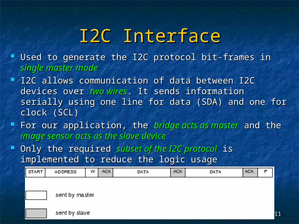
I2C InterfaceI2C Interface Used to generate the I2C protocol bit-frames in Used to generate the I2C protocol bit-frames in single single
master modemaster mode I2C allows communication of data between I2C I2C allows communication of data between I2C
devices over devices over two wirestwo wires. It sends information serially . It sends information serially using one line for data (SDA) and one for clock (SCL) using one line for data (SDA) and one for clock (SCL)
For our application, the For our application, the bridge acts as masterbridge acts as master and the and the image sensor acts as the slave deviceimage sensor acts as the slave device
Only the required Only the required subset of the I2C protocolsubset of the I2C protocol is is implemented to reduce the logic usage implemented to reduce the logic usage

1212
Memory Addressing and Memory Addressing and ControlControl
This block manages the data pins for the image sensor interface This block manages the data pins for the image sensor interface Generates address and control signals for the Memory block of Generates address and control signals for the Memory block of
the bridge. the bridge. It implements a 19 bit It implements a 19 bit address-up counteraddress-up counter and it is and it is
connected with the address bus of the memory. connected with the address bus of the memory. The The DOUT (0:7)DOUT (0:7) is directly connected with the data bus of is directly connected with the data bus of
the memory. the memory. In the valid data state, at each negative edge event of In the valid data state, at each negative edge event of DCLKDCLK, ,
the the address up-counteraddress up-counter is incremented, and at each positive is incremented, and at each positive edge event of edge event of DCLKDCLK,, WR’WR’ signal for the memory is signal for the memory is generated. generated.
After a complete frame is received, the After a complete frame is received, the address up-counter address up-counter is is cleared and cleared and FrameReceicedFrameReceiced signal is asserted high. signal is asserted high.

1313
Random Access MemoryRandom Access Memory A 512KB A 512KB single port random access memorysingle port random access memory
block is used to store a frameblock is used to store a frame

1414
Clock GeneratorClock Generator This block generates the This block generates the 20 MHz clock20 MHz clock at the at the EXTCLKEXTCLK pin, which must pin, which must
be fed in the image sensorbe fed in the image sensor An An 800 KHz clock800 KHz clock is also required to generate the clock for the is also required to generate the clock for the I2C I2C
Interface and the Sensor Control block.Interface and the Sensor Control block. The 800 KHz clock can be The 800 KHz clock can be generated by dividing the generated by dividing the EXTCLKEXTCLK by 25 using a by 25 using a mod-25 countermod-25 counter

1515
OutlineOutline MotivationMotivation The Image Sensor InterfaceThe Image Sensor Interface Proposed Proposed BridgeBridge
Sensor ControlSensor Control I2C InterfaceI2C Interface Memory Addressing and ControlMemory Addressing and Control Random Access MemoryRandom Access Memory Clock GeneratorClock Generator
ResultsResults Conclusion Conclusion

1616
ResultResult The proposed The proposed bridge was modeledbridge was modeled in in VHDLVHDL. . A A model for the image sensormodel for the image sensor implementing implementing
the DVP interface and the DVP interface and an image processoran image processor, , which access the pixels using the proposed which access the pixels using the proposed bridge, was also written. bridge, was also written.
The model was simulated using The model was simulated using ModelSimModelSim and by observing the simulation timing and by observing the simulation timing waveforms, the waveforms, the correctness of the functional correctness of the functional behaviorbehavior of the bridge was verified. of the bridge was verified.

1717
Synthesis ResultSynthesis Result
The maximum allowable frequency for The maximum allowable frequency for DCLKDCLK can vary from can vary from 76.5 MHz to 244.4 MHz.76.5 MHz to 244.4 MHz. The area utilizations are almost the same for all the devices, however, Xilinx Virtex5 occupies The area utilizations are almost the same for all the devices, however, Xilinx Virtex5 occupies
lesser LUT. lesser LUT. The The Memory blockMemory block can be connected can be connected with the embedded RAM blockswith the embedded RAM blocks of the FPGA device, and of the FPGA device, and
the embedded clock generators of the FPGA can be used to generate the required clock signals. the embedded clock generators of the FPGA can be used to generate the required clock signals.

1818
ConclusionConclusion In this work, the design of a novel bridge is In this work, the design of a novel bridge is
proposed to proposed to interface high speed image sensorsinterface high speed image sensors with low power and low speed embedded systems. with low power and low speed embedded systems.
By using the proposed bridge, a frame can be By using the proposed bridge, a frame can be captured and stored in the captured and stored in the bridge’s memorybridge’s memory easily easily without implementing any I2C protocolwithout implementing any I2C protocol in the in the image processor. Then the pixel values can be image processor. Then the pixel values can be accessed by the processor through a accessed by the processor through a parallel parallel memory access interfacememory access interface at at desired speeddesired speed and in a and in a random access fashionrandom access fashion. .
The bridge can support data rate of image sensors The bridge can support data rate of image sensors up to 244.4 MHz in Xilinx Vertex 5 FPGA. up to 244.4 MHz in Xilinx Vertex 5 FPGA.

1919
ThanksThanks

2020
Simulation Waveforms (1/2)Simulation Waveforms (1/2)

2121
Simulation Waveforms (2/2)Simulation Waveforms (2/2)