design of a high powered led driver - cal poly
TRANSCRIPT

Design of a High Powered LED Driver
By
Omar Renteria
EE 460-07
Project Advisor: David B. Braun
Senior Project
ELECTRICAL ENGINEERING DEPARTMENT
California Polytechnic State University
San Luis Obispo
2015

i
TABLE OF CONTENTS
Section Page
List of Figures ................................................................................................................................ iii
List of Tables ................................................................................................................................. vi
Abstract ......................................................................................................................................... vii
I. Introduction ..........................................................................................................................1
II. Customer Needs, Requirements, and Specifications ...........................................................4
III. Functional Decomposition ...................................................................................................5
IV. Design ..................................................................................................................................9
V. LED Driver ........................................................................................................................12
VI. Creating LED PSpice Model .............................................................................................20
VII. Importing Model Files to PSpice .......................................................................................25
VIII. Simulation Results .............................................................................................................27
IX. Board Design .....................................................................................................................30
X. Heat Sink Calculations .......................................................................................................35
XI. Microcontroller ..................................................................................................................39
XII. Assembly............................................................................................................................40
XIII. Testing................................................................................................................................41
XIV. Troubleshooting .................................................................................................................42
XV. Results ................................................................................................................................44
XVI. Future Work .......................................................................................................................48
XVII. References ..........................................................................................................................49

ii
TABLE OF CONTENTS
Section Page
XVIII. Appendices .........................................................................................................................50
A. Senior Project Analysis ......................................................................................................50
B. PSpice Code .......................................................................................................................55

iii
LIST OF FIGURES
Figure 1: LED Driver Gantt Chart Fall 2014 ...................................................................................2
Figure 2: LED Driver Gantt Chart Winter 2015 ..............................................................................2
Figure 3: LED Driver Gantt Chart Spring 2015 ..............................................................................3
Figure 4: Level 0 Block Diagram ....................................................................................................5
Figure 5: Level 1 Block Diagram ....................................................................................................6
Figure 6: Max16834 Evaluation Board..........................................................................................12
Figure 7: Boost LED Driver ..........................................................................................................13
Figure 8: Component Values Spreadsheet .....................................................................................18
Figure 9: Generic PSpice LED Model ...........................................................................................20
Figure 10: Electrical Characteristics of XR-E LED (TJ = 25˚C)...................................................20
Figure 11: Loading Image into WebPlotDigitizer .........................................................................21
Figure 12: Selecting Plot Type ......................................................................................................21
Figure 13: Aligning X-Y Axes ......................................................................................................22
Figure 14: Calibrating Axes ...........................................................................................................22
Figure 15: X-Y Axes Values..........................................................................................................22
Figure 16: Selecting Data Points....................................................................................................23
Figure 17: Excel Electrical Characteristics Plot ............................................................................24
Figure 18: PSpice Model Editor ....................................................................................................25
Figure 19: Export Window ............................................................................................................26
Figure 20: Adding Library File ......................................................................................................26
Figure 21: LED Driver PSpice Schematic .....................................................................................27
Figure 22: Initial PSpice Simulation ..............................................................................................28

iv
Figure 23: Final PSpice Simulation ...............................................................................................29
Figure 24: Board Layout (Top Layer) ...........................................................................................30
Figure 25: PCB Schematic .............................................................................................................31
Figure 26: Board Layout (GND Layer) .........................................................................................31
Figure 27: Board Layout (Power Layer) .......................................................................................32
Figure 28: Board Layout (Bottom Layer) ......................................................................................32
Figure 29: Final Board Layout (Top & Bottom Layer) .................................................................33
Figure 30: Final Board Layout (GND Layer) ................................................................................33
Figure 31: Final Board Layout (Power Layer) ..............................................................................34
Figure 32: Thermal Model of an LED ...........................................................................................35
Figure 33: Heat Sink & Hardware .................................................................................................36
Figure 34: LED Mounted on Heat Sink .........................................................................................36
Figure 35: Power Being Supplied to LED .....................................................................................37
Figure 36: Thermal Images of LED ...............................................................................................37
Figure 37: Thermocouple Location ...............................................................................................38
Figure 38: Type K Thermocouple ..................................................................................................38
Figure 39: Microduino-Core+ ........................................................................................................39
Figure 40: Manufactured circuit board ..........................................................................................40
Figure 41: Finished circuit board ...................................................................................................40
Figure 42: Aoyue 2703A+ Hot-air rework Station ........................................................................40
Figure 43: LEDs connected in series .............................................................................................40
Figure 44: DC power jack and schematic ......................................................................................41
Figure 45: Circuit board PGND vias .............................................................................................42
Figure 46: MAX16834 Pin configuration ......................................................................................43

v
Figure 47: Photo cell used in measuring current ...........................................................................44
Figure 48: Light intensity when duty cycle = 80% ........................................................................44
Figure 49: Photocell current vs Duty cycle plot ............................................................................45
Figure 50: NDRV Voltage .............................................................................................................46
Figure 51: CS Voltage ...................................................................................................................46
Figure 52: Drain voltage of Q1 ......................................................................................................47

vi
LIST OF TABLES
Table 1: Design of a High Power LED Driver Requirements and Specifications ...........................4
Table 2: Functionality Table for Level 0 Block Diagram ................................................................5
Table 3: Functionality Table for Level 1 Block Diagram (Bridge Rectifier) ..................................6
Table 4: Functionality Table for Level 1 Block Diagram (DC-DC Converter) ..............................7
Table 5: Functionality Table for Level 1 Block Diagram (LEDs) ...................................................7
Table 6: Cost Estimate Table ...........................................................................................................8
Table 7: Color Temperature Table .................................................................................................10
Table 8: Buck Converter Characteristics .......................................................................................10
Table 9: Boost Converter Characteristics ......................................................................................10
Table 10: SEPIC Converter Characteristics ...................................................................................11
Table 11: Buck-Boost Converter Characteristics ..........................................................................11
Table 12: CUK Converter Characteristics .....................................................................................11
Table 13: Bill of Materials .............................................................................................................19
Table 14: Photo Cell current measurements .................................................................................44
Table 15: Led String current & Voltage measurements ................................................................45

vii
ABSTRACT
Research has shown that LED lighting products have greater energy efficiency, longer
lifespans, and lower heat outputs than compared with traditional lighting technologies. An
estimated growth of 45 percent per year through 2019 for the LED lighting market should
provide a wider variety of LED related products to consumers. The goal of this project; to create
a driving circuit that powers a set of high powered LEDs. The implementation of LEDs
significantly reduces the power consumption in comparison with other types of light such as
incandescent bulbs or CFLs, therefore saving the consumer money.

1
I. INTRODUCTION
Most sources of light located in a typical home consist of incandescent lamps or compact
fluorescent lamps (CFLs). These light sources have proved inefficient in terms of power use and
output lighting when compared to light emitting diodes [1]. Light emitting diodes are
semiconductor devices that emit light when electrical current passes through it. A light emitting
diode or LED consists of two types of materials called P-type semiconductors and N-type
semiconductors. Current flows from the p-side to the n-side of the diode. The area in between
both materials is called the P-N junction. Charge carriers known as electrons and holes flow into
the junction with different voltages. When one of the electrons meets a hole, it falls into a lower
energy level and releases energy in the form of a photon.
The typical power consumption of an incandescent bulb is 60W and they last an average
of around 1000 hours. Compact fluorescent lamps (CFLs) last an average of around 8000 hours
and consume about 15 watts of power [13]. Incandescent bulbs are very inefficient since a lot of
their energy is wasted as heat. A drawback of CFLs is that they contain mercury which is highly
toxic. This makes CFLs hazardous and hard to dispose of properly without damaging the
environment. The LED is much more efficient than the previously mentioned alternatives. They
have lower power consumption and longer lifespans. LEDs last an average of 50,000 hours or
more and draw less than 8 watts of power.
A minimum of 800 lumens is chosen as the luminous flux output by the system. On
average, a typical 60W incandescent light bulb produces 800 lumens of light [13]. A compact
fluorescent light bulb producing the same light output as the incandescent light bulb only
requires about 15W of power. An LED light bulb having an output of 800 lumens only requires
about 8W to power it. If each of these bulbs were expected to remain on for about 5 hours per
day for a year and the price per KWh of power used is 18.02 cents in the state of California for
September 2014 [14], then the LED bulb would cost about $2.63 to operate. The compact
fluorescent bulb would require about $4.93 to operate for 5 hours every day for a year. The
incandescent bulb would require $19.73 to operate for 5 hours every day for a year. Different
topologies for the DC to DC Converter are researched in order to achieve a final design for the
LED driver [8].
The only problem with LED lighting is that it costs more than incandescent or CFL bulbs.
Replacing every fixture with LED bulbs would prove costly to the homeowner. The system for
this project provides a driving circuit that powers a set of LEDs that run much more efficiently
than standard lighting methods and provides it at lower costs.
2
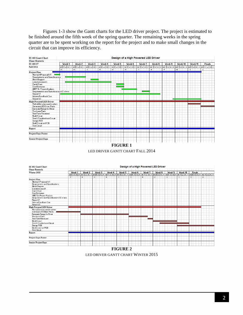
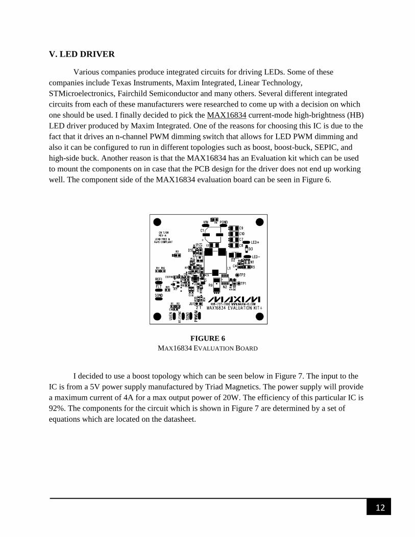
Figures 1-3 show the Gantt charts for the LED driver project. The project is estimated to
be finished around the fifth week of the spring quarter. The remaining weeks in the spring
quarter are to be spent working on the report for the project and to make small changes in the
circuit that can improve its efficiency.
FIGURE 1
LED DRIVER GANTT CHART FALL 2014
FIGURE 2
LED DRIVER GANTT CHART WINTER 2015

3
FIGURE 3
LED DRIVER GANTT CHART SPRING 2015

4
II. CUSTOMER NEEDS, REQUIREMENTS, and SPECIFICATIONS
This system targets students, office workers, and just about anyone who requires a long
lasting and efficient source of light. The overall cost of the system needs to be cheaper than
similar products in the market or it will not attract the consumers’ attention. The customers need
a product that requires as little maintenance as possible. This is achieved through the use of
LEDs. LEDs on average last about 50,000 hours or more [13]. If the LEDs are estimated to stay
on for 5 hours each day in every year then they will need to be replaced every 27 years.
Incandescent bulbs on average last about 1,200 hours [13], and they typically only last for about
a year. Through the use of LED technology, the customer saves money by not having to purchase
replacement bulbs every year. The datasheet of a randomly selected high-powered LED specifies
a maximum junction temperature of 150˚C [1]. The high temperature can significantly impact the
performance of the LEDs. The high temperatures can permanently damage the LED with no heat
sinks present to cool it down.
TABLE 1
DESIGN OF A HIGH POWERED LED DRIVER REQUIREMENTS AND SPECIFICATIONS
Marketing
Requirements
Engineering
Specifications Justification
1 Total system cost to manufacture under
$130.
Cheaper than commercially available products
with the same functionality as this product.
1,3 Dimensions of the driving circuit under
3.8” x 2.5” x 1”.
System fits in the base of a standard lamp.
2,4 Junction temperature lower than 120˚C. Reduced efficiency of the LEDs occurs with
higher temperatures and also run the risk of
permanent damage.
1,2,4 Should have a maximum input power of
20W.
Ensures that the LEDs operate at their highest
efficiency.
1,4 System should produce a minimum of 800
lumens.
The standard 60W LED replacement bulb
emits an average amount of visible light
equivalent to 800 lumens.
1, 3, 5 Total system should weigh under 8 lbs. Weight includes that of the luminaire. Weighs
less than similar products in the market.
4, 6 Color temperature higher than 3000K Typically used in libraries or office areas
Marketing Requirements
1. System should have a low cost
2. System should operate at low temperatures
3. As small as possible
4. System should have a high output power
5. System as light as possible
6. System produces warm white light

5
POWER LIGHT
III. FUNCTIONAL DECOMPOSITION
Figure 4 shows the Level 0 block diagram for the LED Driver. A typical 120V 60Hz
household outlet provides the input to the system. Output of the system is the light produced by
the LEDs.
FIGURE 4
LEVEL 0 BLOCK DIAGRAM
TABLE 2
FUNCTIONALITY TABLE FOR THE LEVEL 0 BLOCK DIAGRAM
MODULE High powered LED Driver
INPUTS Power: 120 V AC 60HZ
OUTPUTS Light: Minimum luminous intensity of 800 Lumens
FUNCTIONALITY To power a set of high powered LEDS efficiently with
minimal power loss.
LED
DRIVER

6
POWER LIGHT
DC VOLTAGE & CURRENT HIGHER/LOWER DC VOLTAGE & CURRENT
Figure 5 shows the Level 1 block diagram for the LED driver circuit. The bridge rectifier
takes the input which is from a household outlet rated at 120 V AC and output a direct
current, which can be used by the DC-to-DC converter to achieve the right voltage
needed in order to power the LEDs. The output of the DC-DC converter is adjusted
depending on the configuration of the LEDs and the amount used. The forward voltage of
each LED at 1A is 3.7V [2]. The DC-to-DC converter being used in this circuit is a boost
converter. The boost converter can produce an output voltage that is greater than its input
[11].
FIGURE 5
LEVEL 1 BLOCK DIAGRAM
TABLE 3
FUNCTIONALITY TABLE FOR THE LEVEL 1 BLOCK DIAGRAM (BRIDGE RECTIFIER)
MODULE Bridge Rectifier
INPUTS Power: 120 V AC 60HZ
OUTPUTS DC voltage and current
FUNCTIONALITY Conversion of alternating current (AC) into direct current
(DC)
Bridge Rectifier
DC-DC Converter
LEDS

7
Table 2 describes the inputs and outputs for the LED driver circuit. The output of the driver will
be light with a minimum intensity of 800 lumens. Table 1 shows the engineering specifications
for the whole system. The color temperature of the LEDs will be around 3000k which is
typically used in libraries or office environments. The color temperature was chosen because the
system is intended to be used in a household. Tables 3-5 show the functionality tables for each of
the three separate modules that make up the LED driver. The tables describe the inputs/outputs
and the overall functionality of each module.
TABLE 4
FUNCTIONALITY TABLE FOR THE LEVEL 1 BLOCK DIAGRAM (DC-DC CONVERTER)
MODULE DC-DC Converter
INPUTS DC voltage and current
OUTPUTS Higher DC voltage and current than input
FUNCTIONALITY Converts a source of direct current from one voltage level to
another.
TABLE 5
FUNCTIONALITY TABLE FOR THE LEVEL 1 BLOCK DIAGRAM (LEDS)
MODULE LEDS
INPUTS DC voltage and current to power LEDS
3.7V at 1A per LED [2]
OUTPUTS Light
FUNCTIONALITY Semiconductor device that emits light when a voltage is
applied to its leads.

8
Table 6 shows the Costs estimate table for the whole driver system. The project is was
finished the week before finals. A total of around 7-10 hours were put into the project per week
depending on the workload for the other classes. This includes labor put into the project by the
student and also time spent by the advisor providing feedback on the project. This accumulates to
a total of about 260 hours of labor put into the creation of the project. Hourly wage was chosen
to be around $20, so total costs in labor come to a total of $5200. The AC to DC converter was
purchased from Digikey. Most of the equipment needed to complete this project was found in the
project labs, but some money had to be spent on additional equipment such as solder, flux, ESD
safe tweezers, and an antistatic wrist strap. The parts list includes the LEDs needed for this
system, the heat sink, and all the parts required to produce the DC to DC Converter.
TABLE 6
COSTS ESTIMATE TABLE
Materials Cost
PCB $112
Parts $78.98
Equipment $39.79
LEDs $41.45
Labor $5,200
Total: $5,472
Costs Estimate

9
IV. DESIGN
The first step in the design process of the LED driver is to pick the type of LED that can
be used and the quantity. I settled with picking out a product from all the different types of LEDs
produced by Cree. Cree is a multinational manufacturer of semiconductor light emitting diodes.
The reason for picking this manufacturer is that the prices of their products are reasonable and
are of good quality.
The Cree XR-E was chosen for the driver because of its price and its light output of 251
lumens at 4 Watts [2]. The next step was to choose the correlated color temperature of the LED
since various options were available. The correlated color temperature (CCT) describes how the
color of the light appears from the light source which is measured in kelvins. The scale ranges
from 1000K which is very red to 10,000K which is very blue. The higher up the scale the light
goes, the closer it resembles blue daylight. Color temperature does not describe the temperature
of the light source but rather it describes the color it produces. Table 7 shown below shows the
color temperature range. There is no wrong choice for color temperature, it all depends on the
consumer’s choice for light. A typical incandescent light bulb emits a yellowish color with a
temperature range between 2700K-3300K [15]. After some research it was determined that a
cool white color temperature would be used. Cool white colors are typically used in office, study,
and retail environments and they provide a cleaner and brighter feel.
The next step was to decide how many of the Cree XR-E LEDs to use in the system. The
goal is to power a lamp that outputs a higher or equal amount of light than a regular incandescent
bulb. A typical 60 Watt incandescent light bulb emits about 800 lumens of visible light. In order
to achieve a light source that emits an equal or greater amount, I will have to wire 4 of those
LEDs in series to achieve a final output of 1004 lumens. This is about a 25.5% increase in
luminous flux than a traditional 60 Watt incandescent bulb.
The forward voltage of each LED is around 3.5V with a maximum drive current of 0.7A.
This requires around 10W to power the LEDs at close to their maximum point.

10
TABLE 7
COLOR TEMPERATURE TABLE
The next step is to choose a topology for the driver. Many different DC-to-DC converter
topologies exist but only the most common were examined. The first topology examined is the
Buck converter. Its pros are that it contains only one switch voltage drop, has low-ripple current
in the output-filter capacitor and it has the lowest peak current of any switching-regulator
configuration [16]. Its cons are that the output voltage must be less than the input voltage and
that it requires a high-side switch. The advantages and disadvantages for each of the other
topologies examined are listed on Tables 8-12. The design of the driver along with the chosen
topology is outlined in the next section.
TABLE 8
BUCK CONVERTER CHARACTERISTICS
TABLE 9
BOOST CONVERTER CHARACTERISTICS
Non-Isolated
Forward: Energy goes from input, through the magnetics & to the load simultaneously
Step Down(Buck): Output voltage is lower than input, and of same polarity
Advantages Disadvantages
Low Switch Stress Potential overvoltage if switch is shorted
Small output filter High side switch drive required
Low ripple High input ripple current
Remarkably efficient 95%
Non-Isolated
Flyback: Energy goes from input & stored in the magnetics. Later, it is released from magnetics to the load.
(Non-inverting)Step Up(Boost): Output voltage is higher than input.
Advantages Disadvantages
Low input ripple current High peak collector current
Regulator loop hard to stabilize
High output ripple
Unable to control short-circuit current

11
TABLE 10
SEPIC CONVERTER CHARACTERISTICS
TABLE 11
BUCK-BOOST CONVERTER CHARACTERISTICS
TABLE 12
CUK CONVERTER CHARACTERISTICS
Non-Isolated
Flyback: Energy goes from input & stored in the magnetics. Later, it is released from magnetics to the load.
(Non-inverting)SEPIC: Output voltage can be lower or higher than input.
Advantages Disadvantages
Low ripple input current Switch has high peakand rms current which limit output power
Step-up/down with n ratio 2 caps used have high ripple current requirements(low ESR)
Capacitive isolation protects against switch failure CCM makes loop stabilization difficult
High output ripple
Non-Isolated
Flyback: Energy goes from input & stored in the magnetics. Later, it is released from magnetics to the load.
(Inverting)Buck-Boost: Output voltage magnitude that is either greater than or less than the input.
Advantages Disadvantages
Voltage inversion without transfomer Regulator loop hard to stabilize
High frequency operation High side switch drive required
High output ripple
High input ripple current
Non-Isolated
Flyback: Energy goes from input & stored in the magnetics. Later, it is released from magnetics to the load.
(Inverting Boost-Buck)Cuk: Output voltage magnitude that is either greater than or less than the input.
Advantages Disadvantages
Low ripple input & output current High drain current
Capacitive isolation protects against switch failure Intermediate capacitor has high ripple current requirement (low ESR)
High voltage required for the switch
12
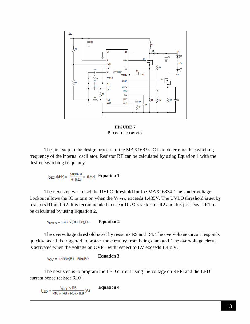
V. LED DRIVER
Various companies produce integrated circuits for driving LEDs. Some of these
companies include Texas Instruments, Maxim Integrated, Linear Technology,
STMicroelectronics, Fairchild Semiconductor and many others. Several different integrated
circuits from each of these manufacturers were researched to come up with a decision on which
one should be used. I finally decided to pick the MAX16834 current-mode high-brightness (HB)
LED driver produced by Maxim Integrated. One of the reasons for choosing this IC is due to the
fact that it drives an n-channel PWM dimming switch that allows for LED PWM dimming and
also it can be configured to run in different topologies such as boost, boost-buck, SEPIC, and
high-side buck. Another reason is that the MAX16834 has an Evaluation kit which can be used
to mount the components on in case that the PCB design for the driver does not end up working
well. The component side of the MAX16834 evaluation board can be seen in Figure 6.
FIGURE 6
MAX16834 EVALUATION BOARD
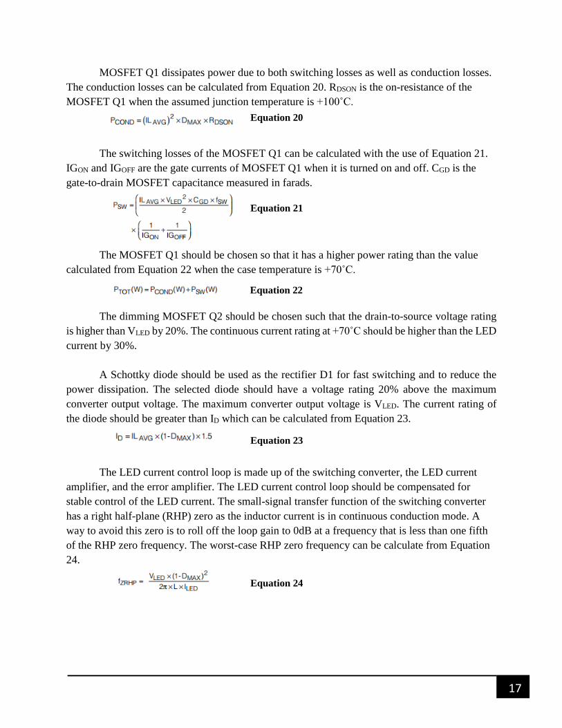
I decided to use a boost topology which can be seen below in Figure 7. The input to the
IC is from a 5V power supply manufactured by Triad Magnetics. The power supply will provide
a maximum current of 4A for a max output power of 20W. The efficiency of this particular IC is
92%. The components for the circuit which is shown in Figure 7 are determined by a set of
equations which are located on the datasheet.
13
Equation 4
Equation 1
Equation 2
Equation 3
FIGURE 7
BOOST LED DRIVER
The first step in the design process of the MAX16834 IC is to determine the switching
frequency of the internal oscillator. Resistor RT can be calculated by using Equation 1 with the
desired switching frequency.
The next step was to set the UVLO threshold for the MAX16834. The Under voltage
Lockout allows the IC to turn on when the VUVEN exceeds 1.435V. The UVLO threshold is set by
resistors R1 and R2. It is recommended to use a 10kΩ resistor for R2 and this just leaves R1 to
be calculated by using Equation 2.
The overvoltage threshold is set by resistors R9 and R4. The overvoltage circuit responds
quickly once it is triggered to protect the circuitry from being damaged. The overvoltage circuit
is activated when the voltage on OVP+ with respect to LV exceeds 1.435V.
The next step is to program the LED current using the voltage on REFI and the LED
current-sense resistor R10.

14
Equation 5
Equation 6
Equation 7
ILED is set to be operating at 0.7A from the CREE X-RE datasheet [2], VREF is given from
the MAX16834 datasheet as 3.7V. Resistor R10 is chosen so that the regulation voltage across it
does not exceed 0.3V. If the voltage across it exceeds 0.3V the LED short-circuit protection
circuit is activated. R5 is also picked making sure that the desired value is available for sale with
tolerances of 1% from the chosen value. All that is needed to program the LED current is to enter
all the previously mentioned values into Equation 4 and solving for R6. The closest value which
could be obtained was a resistor with a resistance of 9.1kΩ.
The next step is to determine the maximum duty cycle of the MAX16834 IC, which will
then be used to calculate the maximum average inductor current, peak-to-peak inductor current
ripple, and the peak inductor current.
VLED is the forward voltage of the LED string in volts. In this case since I will be using
four CREE X-RE LED’s operating at 3.5V at 0.7A, the forward voltage will be 14V. VD is the
forward drop of the rectifier diode D1 which is approximately 0.6V. VINMIN is the minimum input
supply voltage which in this case will be set to 4.75V. VFET is the average drain to source voltage
of the MOSFET Q1 when it is on, an approximate value of 0.2V is recommended by the
datasheet to initially calculate DMAX. Once the power MOSFET is selected, a more accurate
value of the maximum duty cycle can be calculated.
The next step was to determine the minimum inductance value for the inductor L1. A few
values are needed before being able to calculate the inductance value using Equation 9 shown
below. First I needed to find the maximum average inductor current which can be calculated by
using Equation 6. ILED is set to be 0.7A from the CREE XR-E datasheet [2] as was previously
mentioned.
The maximum average inductor current can now be used to obtain the peak-to-peak
inductor current ripple which can be calculated by the use of Equation 7. This equation allows
the peak-to-peak inductor ripple to be about 30% of the average inductor current.

15
Equation 8
Equation 9
Equation 10
Equation 11
Equation 12
Equation 8 shown above represents the peak inductor current measured in amperes.
Once values are calculated from Equations 6-8, then Equation 9 can finally be used to
calculate the minimum inductance value. VINMIN as was mentioned before is the minimum
supply voltage which in this project is set to 4.75V. VFET as was also previously mentioned is the
average drain to source voltage of the MOSFET Q1. An approximate value of about 0.2V is used
initially. Fsw is the switching frequency which is fosc which was calculated in Equation 1. The
chosen inductor has to have a minimum inductance greater than the calculated value and the
current rating of the inductor should be higher than ILP from Equation 8.
Equation 10 can be used to find the value for the switch current-sense resistor. The 0.25
in the numerator is the minimum peak current-sense threshold in volts. The peak inductor current
is multiplied by a factor of 1.25 to provide a 25% margin to account for tolerances. The ISAT of the
inductor should be higher than 0.35V/R8.
The next step is to determine the value of the output capacitor. The function of the output
capacitor is to reduce the output ripple to acceptable values. The parasitic inductance (ESL), the
equivalent series resistance (ESR), and the bulk capacitance of the output capacitor all contribute
to the output ripple. In order to reduce the ESL and ESR effects, multiple capacitors may be
connected in parallel to achieve the required bulk capacitance.
The output capacitance can be calculated by using Equation 11 shown above.
ΔVOUTRIPPLE is the output voltage ripple in volts. The output voltage ripple is chosen to be
150mV which is the same as the input, the input voltage ripple was obtained directly from the
datasheet of the Triad Magnetics power supply being used in this project. The ESR of the output
capacitor can be calculated from Equation 12. The chosen capacitance has to be higher than the
calculated value obtained in Equation 11, and the ESR of the capacitor has to be less than the
value obtained in Equation 12.

16
Equation 13
Equation 14
Equation 15
Equation 16
Equation 17
Equation 18
Equation 19
Equation 13 can be used to calculate the RMS current rating for the output capacitor.
The input capacitor C1 bypasses the ripple current drawn by the converter and helps
reduce the amplitude of high-frequency current being conducted to the input supply. The
parasitic inductance (ESL), the equivalent series resistance (ESR), and the bulk capacitance of
the capacitor all contribute to the input ripple. Low-ESR capacitors that can handle the maximum
input RMS ripple current should be used.
The input capacitance can be calculated directly from Equation 14. ΔVin is the input
ripple, which is obtained directly from the Triad Magnetics power supply datasheet. The ESR of
the input capacitor is calculated with the use of Equation 15.
Equation 16 is used to find the RMS current rating of the input capacitor.
The value for the slope compensation capacitor can be found using Equation 17. VLED is
the voltage of the LED string, which is 14V in this case. Slope compensation is added to
converters with peak current-mode control operating in continuous conduction mode (CCM) to
avoid current loop instability. The capacitor is charged with a 100μA current source, which is
shown in the equation and discharged at the beginning of each switching cycle.
The switching MOSFET Q1 should have a drain-to-source voltage rating higher than the
value calculated from Equation 18. The voltage rating should be sufficient to withstand the
maximum output voltage together with the voltage drop of the diode D1 and any overshoot that
might be caused by parasitic capacitances or inductances. VD is the forward voltage drop of the
diode D1.
The drain current rating of the selected MOSFET should be greater than the value
calculated from Equation 19 when the case temperature is at +70˚C. The MOSFET should be
mounted on a board according to the manufacturer’s specs in order to dissipate heat.
17
Equation 20
Equation 21
Equation 22
Equation 23
Equation 24
MOSFET Q1 dissipates power due to both switching losses as well as conduction losses.
The conduction losses can be calculated from Equation 20. RDSON is the on-resistance of the
MOSFET Q1 when the assumed junction temperature is +100˚C.
The switching losses of the MOSFET Q1 can be calculated with the use of Equation 21.
IGON and IGOFF are the gate currents of MOSFET Q1 when it is turned on and off. CGD is the
gate-to-drain MOSFET capacitance measured in farads.
The MOSFET Q1 should be chosen so that it has a higher power rating than the value
calculated from Equation 22 when the case temperature is +70˚C.
The dimming MOSFET Q2 should be chosen such that the drain-to-source voltage rating
is higher than VLED by 20%. The continuous current rating at +70˚C should be higher than the LED
current by 30%.
A Schottky diode should be used as the rectifier D1 for fast switching and to reduce the
power dissipation. The selected diode should have a voltage rating 20% above the maximum
converter output voltage. The maximum converter output voltage is VLED. The current rating of
the diode should be greater than ID which can be calculated from Equation 23.
The LED current control loop is made up of the switching converter, the LED current
amplifier, and the error amplifier. The LED current control loop should be compensated for
stable control of the LED current. The small-signal transfer function of the switching converter
has a right half-plane (RHP) zero as the inductor current is in continuous conduction mode. A
way to avoid this zero is to roll off the loop gain to 0dB at a frequency that is less than one fifth
of the RHP zero frequency. The worst-case RHP zero frequency can be calculate from Equation
24.
18
Equation 25
Equation 26
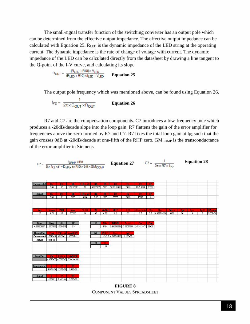
Equation 27 Equation 28
The small-signal transfer function of the switching converter has an output pole which
can be determined from the effective output impedance. The effective output impedance can be
calculated with Equation 25. RLED is the dynamic impedance of the LED string at the operating
current. The dynamic impedance is the rate of change of voltage with current. The dynamic
impedance of the LED can be calculated directly from the datasheet by drawing a line tangent to
the Q-point of the I-V curve, and calculating its slope.
The output pole frequency which was mentioned above, can be found using Equation 26.
R7 and C7 are the compensation components. C7 introduces a low-frequency pole which
produces a -20dB/decade slope into the loop gain. R7 flattens the gain of the error amplifier for
frequencies above the zero formed by R7 and C7. R7 fixes the total loop gain at fP2 such that the
gain crosses 0dB at -20dB/decade at one-fifth of the RHP zero. GMCOMP is the transconductance
of the error amplifier in Siemens.
FIGURE 8
COMPONENT VALUES SPREADSHEET

19
Figure 8 shows an excel file that was created in order to keep all the equations for finding
the component values organized. This made it a lot easier to see what component values changed
when some of the initial parameters had to be updated. Table 13 shows the Bill of Materials for
the LED driver circuit. An extra set of parts was ordered as a backup just in case some of the
parts malfunction, get lost, or get damaged in the process of soldering them to the board.
TABLE 13
BILL OF MATERIALS
Once the component values are obtained for the driver, the next step is to simulate it. The
following section outlines the steps needed in order to create a model for the Cree XR-E LED so
that the driver can be simulated.

20
VI. CREATING LED PSPICE MODEL
In order to create a simulation for the LED driver, I needed to obtain a model for the Cree
XR-E LED. I was able to find the model for an Xlamp ML-E which is another type of LED
produced by Cree. After looking at the file and doing some research I found out that I just
needed to change the IS, N, and RS parameters shown in Figure 9 to closely match those of the
XR-E LED in order to obtain the same IV characteristics as those found in the datasheet which is
shown in Figure 10. In order to find the saturation current (IS) and the emission coefficient (N), I
had to obtain as many points as possible from the IV curve in Figure 10 and plot them in excel.
An application for Google Chrome called WebPlotDigitizer was used to find as many points on
the curve as possible with very high accuracy. A screenshot was first taken of the IV curve and
cropped and saved as a jpeg file. It was then loaded into the application by selecting load image
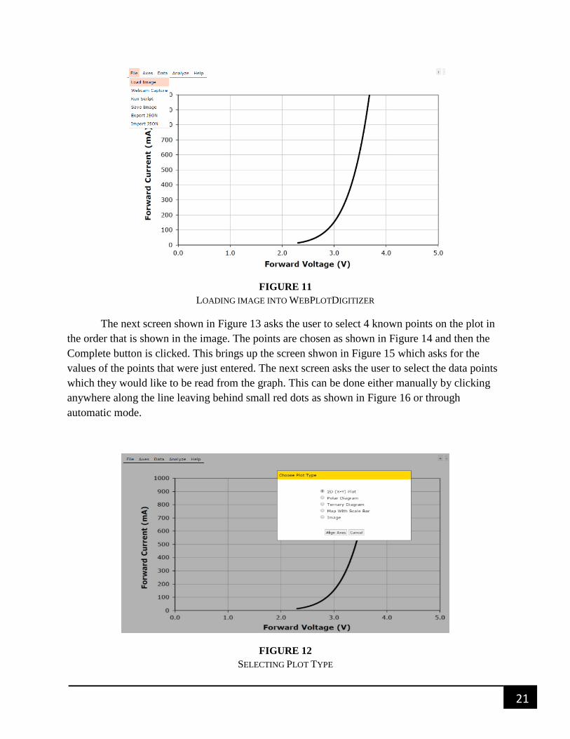
under the File setting on the top left corner of the screen as shown in Figure 11. Once the image
is selected, the next step was to click on 2D(X-Y) Plot and click on align axis as shown in Figure
12.
FIGURE 9
GENERIC PSPICE LED MODEL
FIGURE 10
ELECTRICAL CHARACTERISTICS OF XR-E LED (TJ = 25 ˚C)
21
FIGURE 11
LOADING IMAGE INTO WEBPLOTDIGITIZER
The next screen shown in Figure 13 asks the user to select 4 known points on the plot in
the order that is shown in the image. The points are chosen as shown in Figure 14 and then the
Complete button is clicked. This brings up the screen shwon in Figure 15 which asks for the
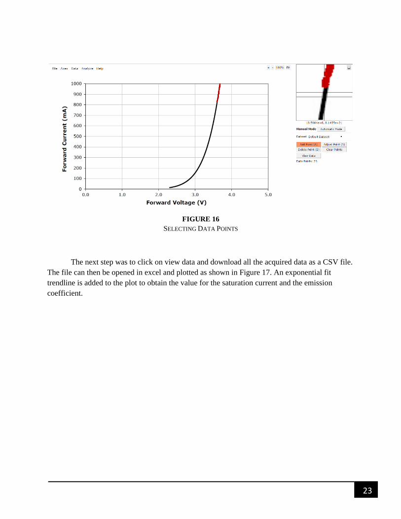
values of the points that were just entered. The next screen asks the user to select the data points
which they would like to be read from the graph. This can be done either manually by clicking
anywhere along the line leaving behind small red dots as shown in Figure 16 or through
automatic mode.
FIGURE 12
SELECTING PLOT TYPE

22
FIGURE 13
ALIGNING X-Y AXES
FIGURE 14
CALIBRATING AXES
FIGURE 15
X-Y AXES VALUES
23
FIGURE 16
SELECTING DATA POINTS
The next step was to click on view data and download all the acquired data as a CSV file.
The file can then be opened in excel and plotted as shown in Figure 17. An exponential fit
trendline is added to the plot to obtain the value for the saturation current and the emission
coefficient.

24
The saturation current is the value shown underlined in red in Figure 17. The emission
coefficient is found by using an equation that is set equal to the value underlined in blue and
solving for N. The SPICE model for the LED matches that of the diode equation shown below.
The underlined portion shown in blue is set equal to the power which e is raised to in the
equation shown below. Since all the values needed for the model to behave as the Cree XR-E
LED have been found, all that is needed is to go back to the model file shown in Figure 9 and to
enter the new values for IS, N, and RS. Section VII explains how to enter the model files into the
circuit simulation software.
𝐼𝑓 = 𝐼𝑆 ∗ (𝑒𝑉𝑓
𝑁∗𝑉𝑡 − 1)
3.1007𝑉𝑓 = 𝑉𝑓
𝑁 ∗ 𝑉𝑡
3.1007 = 1
𝑁 ∗ 0.026
𝑵 = 𝟏𝟐. 𝟒𝟎𝟒𝟏
FIGURE 17
EXCEL ELECTRICAL CHARACTERISTICS PLOT

25
VII. IMPORTING MODEL FILES TO PSPICE
Once all the model files for the components are obtained, the next step is to export them
into model files that can be used by OrCAD Capture in order to be able to layout the circuit. The
library files can only be opened one at a time in the Model Editor. The library file for the
MAX16834 integrated circuit once loaded into the Model Editor can be seen in Figure 18.
FIGURE 18
PSPICE MODEL EDITOR
Once the file is opened in the Model Editor, the next step is to go under File and select
Export to Capture Part Library as shown in Figure 19. This brings up a new window which asks
where to save the output file which has an .olb extension. The new file needs to be added to the
library folder which can be found at OrCAD\OrCAD_16.6_Lite\tools\capture\library. The
component can now be added in PSpice by clicking on Place and clicking on Part, the library file
can be selected by clicking on the button shown in Figure 20 and then the desired component can
now be added to the schematic. Once all the models are added to PSpice, a simulation can finally
be ran and the results are shown in the next section.

26
FIGURE 19
EXPORT WINDOW
FIGURE 20
ADDING LIBRARY FILE
27
VIII. SIMULATION RESULTS
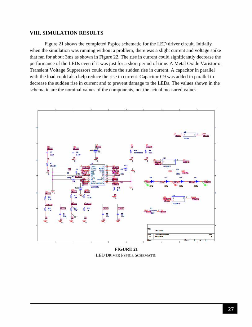
Figure 21 shows the completed Pspice schematic for the LED driver circuit. Initially
when the simulation was running without a problem, there was a slight current and voltage spike
that ran for about 3ms as shown in Figure 22. The rise in current could significantly decrease the
performance of the LEDs even if it was just for a short period of time. A Metal Oxide Varistor or
Transient Voltage Suppressors could reduce the sudden rise in current. A capacitor in parallel
with the load could also help reduce the rise in current. Capacitor C9 was added in parallel to
decrease the sudden rise in current and to prevent damage to the LEDs. The values shown in the
schematic are the nominal values of the components, not the actual measured values.
FIGURE 21
LED DRIVER PSPICE SCHEMATIC

28
Capacitor C9 was calculated by using the following equation:
𝑖 = 𝐶 𝑑𝑉
𝑑𝑡 → 𝐶 = 1𝐴
3𝑚𝑠
15𝑉
The current rose to an amp and the voltage rose to about 15V, the time that the sudden
rise occurred at was for about three milliseconds. These parameters were entered into the above
equation and a capacitor value of about 200μF was obtained.
FIGURE 22
INITIAL PSPICE SIMULATION
The value for C9 was then added to the schematic and the simulation was run again to
check the results. Figure 23 shows the new output voltage and current without the sudden initial
peaks.
Some problems encountered during the design process of the LED driver are that the
dynamic impedance of the LED string was not given in the datasheet. The dynamic impedance is
used to find the effective output impedance of the driver which is then used to calculate the
output pole frequency. The output pole frequency can then be used to calculate R7 and C7. In
order to find the dynamic impedance, a line tangent to the Q-point had to be drawn on the IV
curve of the LED shown in Figure 10. The slope was then calculated and multiplied by four to
obtain the dynamic impedance of the whole string of LEDs. Another problem is that the output
of the driver was too low, the output would show the current as being in Pico amps which

29
suggested that the driver was off. The problem was that the PWMDIM pin was connected to
ground, the datasheet specifies that the pin has to be higher than 1.435V in order for the dimming
MOSFET to turn on. The problem was solved by tying PWMDIM to the input voltage which is
set at 5V. Another problem that was encountered after PWMDIM was tied to Vin is that the
simulation was having convergence problems. After consulting Introduction to PSpice Using
OrCAD for Circuits and Electronics by Muhammad H. Rashid, it was determined that RELTOL
had to be changed to 0.01 and ITL4 had to be changed to 50 under Options in the Simulation
Settings. After these changes the simulation was finally able to run and produced the plot shown
in Figure 22. The PSpice model files and the Netlist for the LED Driver can be found in
Appendix B. Once the simulation is running, the next step is to design a board that holds all the
components in place. The design of the printed circuit board is outlined in the next section.
FIGURE 23
FINAL PSPICE SIMULATION
30
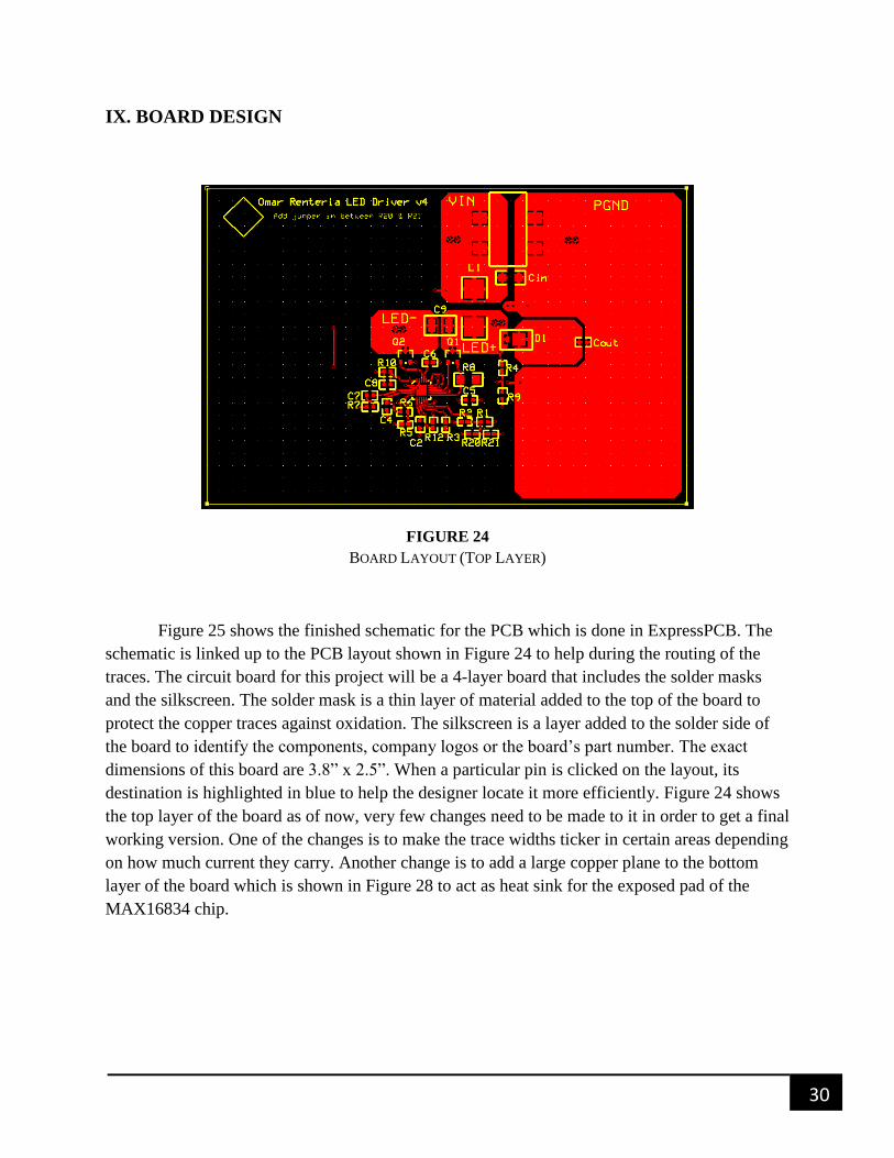
IX. BOARD DESIGN
FIGURE 24
BOARD LAYOUT (TOP LAYER)
Figure 25 shows the finished schematic for the PCB which is done in ExpressPCB. The
schematic is linked up to the PCB layout shown in Figure 24 to help during the routing of the
traces. The circuit board for this project will be a 4-layer board that includes the solder masks
and the silkscreen. The solder mask is a thin layer of material added to the top of the board to
protect the copper traces against oxidation. The silkscreen is a layer added to the solder side of
the board to identify the components, company logos or the board’s part number. The exact
dimensions of this board are 3.8” x 2.5”. When a particular pin is clicked on the layout, its
destination is highlighted in blue to help the designer locate it more efficiently. Figure 24 shows
the top layer of the board as of now, very few changes need to be made to it in order to get a final
working version. One of the changes is to make the trace widths ticker in certain areas depending
on how much current they carry. Another change is to add a large copper plane to the bottom
layer of the board which is shown in Figure 28 to act as heat sink for the exposed pad of the
MAX16834 chip.

31
FIGURE 25
PCB SCHEMATIC
Figure 26 shows the ground layer of the board, the top portion which is separated by the
dark lines is the power ground while the smaller area located at the bottom is the signal ground.
The signal and power ground come together at a location which is very close to the MAX16834
chip. Figure 27 is the power layer of the board, it will not be used in this design so most of the
copper is eliminated from the middle of the board to prevent a short.
FIGURE 26
BOARD LAYOUT (GND LAYER)

32
FIGURE 27
BOARD LAYOUT (POWER LAYER)
FIGURE 28
BOARD LAYOUT (BOTTOM LAYER)

33
FIGURE 29
FINAL BOARD LAYOUT (TOP & BOTTOM LAYER)
FIGURE 30
FINAL BOARD LAYOUT (GND LAYER)
Figure 29 shows the final layout of the board, it shows both the top and bottom layers of
the board. There were a few major and minor changes to the board. One of the biggest changes
was that the 4th revision shown in Figure 24 shows the output of the circuit which is labeled as
LED+ is tied to the output of the inductor, this is completely wrong. Looking back at the
schematic of the LED driver in Figure 7, it is shown that the output of the inductor is connected
to the anode of the diode and the cathode is the one that is tied to LED+. The LED+ pad had to
be moved closer to the LED- pad in order to add the two bypass capacitors labeled as C9-1 and

34
C9-2 between them. The two capacitors are added in order to prevent high current spikes from
damaging the LEDs upon powering up the circuit. Another change is that a Molex connector is
added to the left side of the board in order to allow the LEDs to be easily disconnected from the
board. Another minor change is that test points were added to the board in order to allow
connections to be made directly to the board for testing purposes. The copper plane located
directly under the IC on the bottom layer of the board shown in Figure 28 was removed, instead
4 thermal vias were added to the exposed pad of the IC which are connected to the ground plane
to provide a larger area for heat dissipation. Several vias are also added connecting PGND to the
2nd layer which is the GND layer shown in Figure 30. Another change is that two vias are added
in between resistors 20 and 21 to connect a male header in between them. This is done in order
so that a jumper can be added to the male header in order to power on the chip by adding an
active high signal directly from the chip or so that an external PWM signal can be connected in
order to control the brightness of the LEDs.
Figure 30 shows the ground layer of the circuit board. The lines separating the signal
ground from the power ground are rearranged so that some of the signals from the components
don’t have to travel far.
FIGURE 31
FINAL BOARD LAYOUT (POWER LAYER)
The power layer shown in Figure 31 was mostly the same, the only difference from the
previous version which is shown in Figure 27 is that all the copper was removed in order to
prevent shorts between the other layers of the board when vias are added connecting separate
layers together. The next section outlines the process through which the heatsinks are chosen so
that the LEDs operate well beneath their junction temperature.

35
X. HEAT SINK CALCULATIONS
Most of the electricity in an LED turns into heat rather than light. About 70% of the
electricity is converted into heat while the remaining 30% is turned into light. If the heat is not
removed, then the LED can run at very high temperatures and possibly have its efficiency
reduced or maybe even stop working. Mostly all the heat in an LED is generated at the PN
junction by electrical energy that was not converted into light. One way to reduce the junction
temperature is through the use of a heat sink which helps dissipate the heat from the junction to
the solder point, and from the solder point to the board, the board then transfers the heat to the
heat sink. In order to determine what type of heat sink I need, I first had to find out of the
thermal resistance of the heat sink that will help keep the junction temperature of the LED under
the required amount. Figure 32 shows the thermal model of an LED, Tj is the junction
temperature and Ta is the ambient temperature.
FIGURE 32
THERMAL MODEL OF AN LED
The junction temperature of the Cree XR-E LED is determined to be a maximum of 150˚C from
the datasheet. Since I never want to reach the maximum junction temperature of the LED, I will
use a much smaller value of 60˚C for calculation purposes. The forward current of each LED is
700mA and the forward voltage is 3.5V which are both obtained from the datasheet. The total
power dissipated by the LED is 2.45W which is calculated by multiplying the forward voltage by
the forward current. The ambient temperature is 25˚C and the thermal resistance Rj-c of the LED
is 8˚C/W. The thermal resistance of the thermal pad is 1˚C/W which is obtained from the
datasheet. The following calculations show how the thermal resistance of the heat sink is
calculated.
𝑇𝑐 = 𝑇𝑗 − (𝑅𝑗 − 𝑐 ∗ 𝑃𝑑)
𝑇𝑐 = 60 − (8 ∗ 2.45)
𝑇𝑐 = 𝟒𝟎. 𝟒˚𝑪

36
𝑇𝑏 = 𝑇𝑐 − (𝑅𝑏 ∗ 𝑃𝑑)
𝑇𝑏 = 40.4 − (1 ∗ 2.45)
𝑇𝑏 = 𝟑𝟕. 𝟗𝟓˚𝑪
𝑅ℎ = (𝑇𝑏 − 𝑇𝑎)/𝑃𝑑
𝑅ℎ = (37.95 − 25)/2.45
𝑅ℎ = 𝟓. 𝟐𝟗˚𝑪/𝑾
The thermal resistance of the heat sink required is calculated to be 5.29˚C/W, a heat sink
with a thermal resistance less than the calculated value needs to be picked. I decided to go with
the Wakefield-Vette 882-50AB heat sink which has a thermal resistance of 4.33˚C/W.
FIGURE 33
HEAT SINK & HARDWARE
Figure 33 shows the Wakefield-Vette heat sink that will be used for the Cree XR-E LEDs
on the far right. The star board on which the LED is mounted on is located in the middle and the
thermal pad which secures the star board to the heat sink is shown in the far left. The star board
will also be secured to the heat sink with the help of six 4-40 screws.
FIGURE 34
LED MOUNTED ON HEAT SINK

37
Figure 34 shows the star board with the LED mounted on the heat sink on the left, and it
shows the LED while it is being supplied approximately 3.3V at 700mA on the right. Figure 35
shows that the LED is being powered by around 2.303W while being supplied with 3.3V at
700mA.
FIGURE 35
POWER BEING SUPPLIED TO LED
FIGURE 36
THERMAL IMAGES OF LED

38
Figure 36 shows some thermal images of the LED taken with a Fluke Ti95 Thermal
Imager. The picture to the left was taken right before powering the LED which and it was at
room temperature. The middle picture shows the whole heat sink and LED when it is being
powered by approximately 3.3V at 700mA. The picture located on the right shows a close up of
the LED and it shows that the surface of the LED is operating at approximately 114˚F. These
temperatures do not represent the junction temperature of the LED. In order to find the junction
temperature of the LED I will need to use a thermocouple at the designated spot shown in Figure
37. A thermocouple is made of two thin metal wires that are composed of two different types of
metal. The ends of the two wires are welded together and the leads are separated with insulation
so that only the welded portion is in contact with the test point. Once the welded point is heated
or cooled, it creates a DC voltage differential between the two metals. The voltage is then
converted into a temperature reading by a thermometer.
FIGURE 37
THERMOCOUPLE LOCATION
Thermocouple types are determined according to the type of metals from which they are
made. Figure 38 shows a model for a type k thermocouple which is composed of Nickel-
Chromium for the +lead and Nickel-Aluminum for the –lead.
FIGURE 38
TYPE K THERMOCOUPLE
Once the solder-point temperature is measured with the thermocouple, the following
equation can be used to determine the junction temperature of the LED. Tsp is the solder-point
temperature, θth is the thermal resistance of the LED, and Ptotal is the total power input to the
LED.
𝑇𝑗 = 𝑇𝑠𝑝 + 𝜃𝑡ℎ ∗ 𝑃𝑡𝑜𝑡𝑎𝑙

39
XI. MICROCONTROLLER
The MAX16834 offers a dimming input which can be used for pulse-width modulating
the output current. PWM dimming can be achieved by driving the PWMDIM pin with a
pulsating voltage source. Pulse-width modulation can be implemented using a microcontroller. I
will be looking into producing a PWM signal with a microcontroller and varying its duty cycle to
control the dimming input of the MAX16834. I will be using the Microduino-Core+ which is
about the size of a quarter and it is compatible with the Arduino development environment. The
varying duty cycle can be achieved through the use of a potentiometer and coding through the
Arduino development environment. A picture of the Microduino can be seen in Figure 39.
FIGURE 39
MICRODUINO-CORE+

40
XII. ASSEMBLY
FIGURE 40 FIGURE 41
MANUFACTURED CIRCUIT BOARD FINISHED CIRCUIT BOARD
Figure 40 shows the final version of the printed circuit board once I received it from the
fabrication house. The IC shown in the middle was soldered on campus with the use of a reflow
oven. The temperature profile of the solder was obtained from the datasheet and was
programmed into the reflow oven so that it would melt and flow smoothly across the solder pad.
The big components such as the DC connector, inductor, Molex connector, and test points were
soldered with a soldering iron. The smaller components were soldered on with the help of a hot-
air rework station such as the one pictured in Figure 42. Thermal paste was added to each pad
and the small components where placed with the use of fine tip ESD safe tweezers onto each
pad. The hot-air gun was then carefully used to heat the solder and wait until the surface tension
of the solder aligns the component in the pads. After each component was soldered, I verified
with a multimeter that it was making a solid connection with the pads. The four LEDs connected
in series that will be powered by the driver are shown in Figure 43. The LEDs are mounted onto
the starboard with the help of the hot-air gun since the pads are located underneath the LED and
are then mounted on the heat sink with the thermal pads shown in Figure 33. After soldering the
components, the next step was to test the board. The testing process is outlined in section XIII.
FIGURE 42 FIGURE 43
AOYUE 2703A+ HOT-AIR REWORK STATION LEDS CONNECTED IN SERIES
XIII. TESTING

41
Unfortunately, the junction temperature of the LED was not able to be measured. The
multimeter which included a thermocouple that was available for use in the power lab was not
functioning. Upon inspection, I found out that the batteries corroded inside of the multimeter and
damaged the tabs that provide power from the battery to the circuitry therefore rendering it
useless. The internal components could have also possibly been damaged if some of the solution
found inside of the battery made its way to the inside of the multimeter. A Fluke Ti95 Thermal
Imager was used instead to check the external temperature of the LED, this does not provide a
measurement of the junction temperature but it provided me with an actual measurement of
temperature at which the LEDs were operating in. The LEDs were then connected to a power
supply to briefly supply power to them to make sure that they were functioning properly before
being connected to the driver. As previously mentioned, every component was checked with a
multimeter after it was soldered to make sure that it made contact with the pads. The resistance
of each resistor was also measured after being soldered to make sure that it was the right value.
The last step before connecting the supply to the DC power jack was to verify its polarization.
The datasheet indicated that the power jack had negative center polarization. This means that the
center conductor labeled as 3 which is shown in the pinout diagram in Figure 44 should be
connected to ground. Pins 1 and 2 should both be connected to the input voltage. A multimeter
was used to make sure that the center conductor was connected to ground on the circuit board
and that the inner conductor was tied to VIN. After this was confirmed then the next step was to
power it on with the power supply and troubleshoot it if any problems came up. Troubleshooting
of the circuit is explained in the next section.
FIGURE 44
DC POWER JACK AND SCHEMATIC
XIV. TROUBLESHOOTING

42
After all the components were soldered onto the board, the first step was to power up the
circuit with the LEDs connected to the output of the board. As soon as the power supply was
connected, nothing happened to the circuit. The first thing was to check the actual voltage being
provided by the supply by connecting a multimeter across VIN and PGND shown in Figure 29. I
checked the socket by connecting a phone charger and seeing if it charged my phone. It did, so
my next step was to verify that the power supply was working. I checked the voltage from the
power supply and confirmed that it was working. I did a visual inspection of the board and
everything seemed fine, so I did a continuity check with the multimeter at several points on the
board. I immediately found out that the vias that I added to the ground plane shown below in
Figure 45 with the black box around them were not actually connected to the power supply
ground. This created no path for the current to flow through. This could have been easily solved
before sending off the PCB to be manufactured by turning those vias into thermal vias so they
could connect the top PGND plane with the ground plane. The problem was solved by soldering
a small wire to one of the vias and soldered to the test point shown in Figure 45 with the green
circle around it. Once this was done, the connection was tested with a multimeter.
FIGURE 45
CIRCUIT BOARD PGND VIAS
The power supply was once again connected to the DC power jack and the circuit did not
power on. I used the multimeter to check the voltages at various points on the circuit and saw
that the chip was not being powered on. Upon inspecting the datasheet, it was suggested by my
advisor to check the FLT pin of the IC. The FLT pin is an active-low, open-drain fault indicator
that asserts when there is an overvoltage across the LED string, short-circuit condition across the
LED string, or over temperature. OVP+ is the overvoltage protection pin, it sets the overvoltage
threshold limit across the LEDs.
43
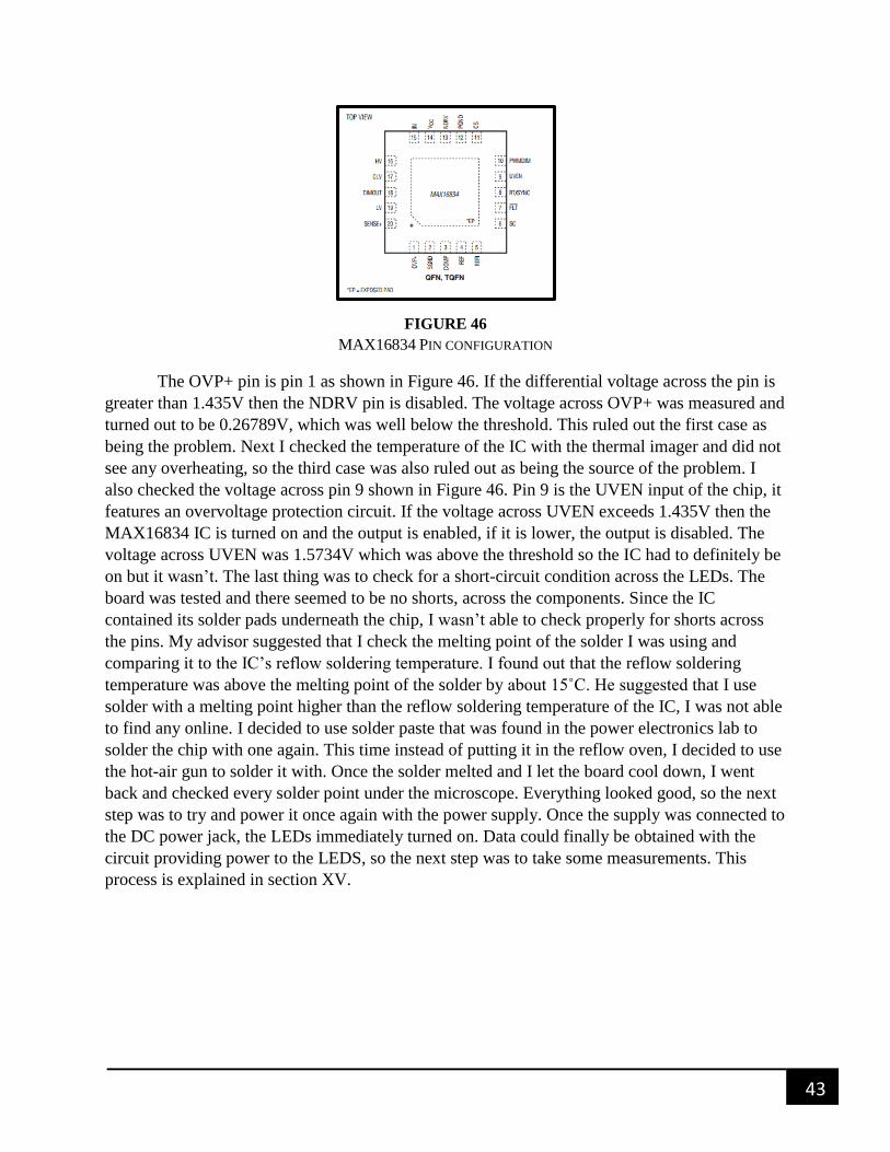
FIGURE 46
MAX16834 PIN CONFIGURATION
The OVP+ pin is pin 1 as shown in Figure 46. If the differential voltage across the pin is
greater than 1.435V then the NDRV pin is disabled. The voltage across OVP+ was measured and
turned out to be 0.26789V, which was well below the threshold. This ruled out the first case as
being the problem. Next I checked the temperature of the IC with the thermal imager and did not
see any overheating, so the third case was also ruled out as being the source of the problem. I
also checked the voltage across pin 9 shown in Figure 46. Pin 9 is the UVEN input of the chip, it
features an overvoltage protection circuit. If the voltage across UVEN exceeds 1.435V then the
MAX16834 IC is turned on and the output is enabled, if it is lower, the output is disabled. The
voltage across UVEN was 1.5734V which was above the threshold so the IC had to definitely be
on but it wasn’t. The last thing was to check for a short-circuit condition across the LEDs. The
board was tested and there seemed to be no shorts, across the components. Since the IC
contained its solder pads underneath the chip, I wasn’t able to check properly for shorts across
the pins. My advisor suggested that I check the melting point of the solder I was using and
comparing it to the IC’s reflow soldering temperature. I found out that the reflow soldering
temperature was above the melting point of the solder by about 15˚C. He suggested that I use
solder with a melting point higher than the reflow soldering temperature of the IC, I was not able
to find any online. I decided to use solder paste that was found in the power electronics lab to
solder the chip with one again. This time instead of putting it in the reflow oven, I decided to use
the hot-air gun to solder it with. Once the solder melted and I let the board cool down, I went
back and checked every solder point under the microscope. Everything looked good, so the next
step was to try and power it once again with the power supply. Once the supply was connected to
the DC power jack, the LEDs immediately turned on. Data could finally be obtained with the
circuit providing power to the LEDS, so the next step was to take some measurements. This
process is explained in section XV.

44
XV. RESULTS
Once the LEDs turned on, I went ahead and obtained some data from the working circuit.
The first step was to make sure that the PWMDIM input worked to make sure that it was
dimming the LEDs. The jumper was disconnected and a 3V peak-to-peak signal with a
frequency of 100 kHz was input into one of the pins. The duty cycle was adjusted to 80% and
then the photo cell shown in Figure 47 was connected to a multimeter to measure the current.
The current of the photo cell is measured because it is directly proportional to the amount of light
emitted by the source, but there is no conversion factor that relates both. Figure 48 shows how
bright the LEDs appear when an 80% duty cycle signal is inserted to PWMDIM.
FIGURE 47 FIGURE 48
PHOTO CELL USED IN MEASURING CURRENT LIGHT INTENSITY WHEN DUTY CYCLE = 80%
The photo cell was then used to measure the current at the various duty cycle intervals
shown in Table 14. A duty cycle of zero corresponds to the current measured when the circuit
was off, so it was only detecting the lighting in the room. Just from the data shown in Table 14, it
is confirmed that the intensity of the light increases as the duty cycle is also increased.
TABLE 14
PHOTO CELL CURRENT MEASUREMENTS
Duty Cycle (%) Photo cell current (mA)
0 0.1775
20 1.0267
30 1.9475
40 2.3924
50 3.4735
60 4.3781
70 6.1168
80 6.7733

45
The data found in Table 14 was plotted and shown in Figure 49 just to see a visual
representation of how much the intensity of the light increases as the duty cycle is changed by
10% intervals.
FIGURE 49
PHOTOCELL CURRENT VS DUTY CYCLE PLOT
Once the current of the photo cell was measured at each interval, the current and voltage
of the LED string were measured at each interval of the duty cycle using a multimeter. The
results are shown in Table 15.
TABLE 15
LED STRING CURRENT & VOLTAGE MEASUREMENTS
0
1
2
3
4
5
6
7
8
0 20 40 60 80 100
Ph
oto
cell
curr
en
t (m
A)
Duty Cycle (%)
Duty Cycle Voltage (V) Current (mA)
20% 11.214 67.826
30% 11.605 139.36
40% 11.926 225.1
50% 12.186 324.65
60% 12.399 426.64
70% 12.818 736.84
80% 12.931 831.79

46
Figure 50 shows the NDRV output of the IC, NDRV is connected to the gate of the IC
and the voltage drives the MOSFET Q1. From the datasheet it is specified that NDRV swings
from VCC and PGND. In this case VCC is referring to VIN which is the input voltage of the
power supply which turns out to be 5V. From Figure 50 one can see that the voltage swings from
5.1V to ground.
FIGURE 50
NDRV VOLTAGE
Figure 51 shows the voltage waveform taken at the source of Q1, it is also connected to
the current-sense input CS. The voltage at CS is used to terminate the on pulse width of the
switching cycle which allows for peak current-mode control.
FIGURE 51
CS VOLTAGE

47
Figure 52 shows the voltage at the output of the inductor which is also connected to the
drain of Q1. During each on state of the cycle the output voltage is seen across the inductor, the
frequency is 498 kHz which is really close to the oscillating frequency of the IC which was
programmed to be 500 kHz.
FIGURE 52
DRAIN VOLTAGE OF Q1
The power consumed by a typical incandescent lightbulb is about 60W. From Table 15,
the total power consumed by the LEDs is about 10.76W at 80% duty cycle. This is six times less
than the power consumed by the incandescent lightbulb. I was not able to measure the light
intensity of the LEDs to verify that it met my initial requirements of a minimum of 800 lumens
due to not having the right equipment to do so. 800 lumens is what a typical incandescent
lightbulb emits, the system did appear to provide more light than a lightbulb but without actual
values it cannot be verified.
Upon doing further research, I was able to find a 60W equivalent dimmable LED
lightbulb. This type of bulb is manufactured by CREE which is also the manufacturer of the
LEDs that I used in this project. The total cost of the project excluding labor, was $272. The cost
of the dimmable LED bulb is $4.97. The dimming feature of the LED bulb cannot be used since
most desk lamps do not contain a dimming feature or homes are also not equipped with dimming
controls.

48
XVI. FUTURE WORK
There were a couple of additional features that I will be implementing to this project in
the future. As I previously mentioned, I added a male header in between resistors 20 & 21 which
is connected directly to PWMDIM. PWMDIM is a dimming input pin which needs to have a
voltage higher than 1.435V in order to turn the dimming MOSFET on. When a jumper is added
to the male headers, the LEDs can be powered directly from the reference voltage of the
MAX16834 IC. When the jumper is removed, the LEDs can be dimmed by adding a PWM
signal directly to one of the male headers and varying the duty cycle of the signal. The original
idea was to obtain the varying PWM signal from a microcontroller as explained in section 11 but
it can also be generated through a 555 timer IC.
I will be adding the whole project into an enclosure so that it more closely resembles a
luminaire and I will also be placing the four heat sinks on a metal plate in order to mount the
LEDs to the luminaire and in order to further dissipate heat. I will also be adding a switch to the
project so that the driver can be turned off easily without having to play with the PWM in order
to turn off the circuit. I will also look into purchasing a multimeter that contains a thermocouple
in order to be able to measure the junction temperature of the LEDs and make sure that the heat
sinks are keeping them well below their maximum value.
I will also look into adding a connector to each LED so that it can be easily removed in
the case that one of them fails. Each LED is connected in series so if one of them were to fail, the
rest of them would not work. I will also look into measuring the light output to make sure that it
met my specifications.

49
XVII. REFERENCES
[1] Pramod Dige, “LED Lighting Market Size, Share, Growth, Trends and Forecasts 2013-2019,” linkedin.com, para. 2,
May 30, 2014. [Online]. Available: https://www.linkedin.com/today/post/article/20140530103750-173774513-led-
lighting-market-size-share-growth-trends-and-forecasts-2013-2019 [Accessed Oct. 12, 2014].
[2] CREE, “XLamp”, XR-E Datasheet, July 2007 [Revised Aug. 2012].
Available: http://www.cree.com/LED-Components-and-Modules/Products/XLamp/Discrete-Directional/XLamp-XRE
[3] Steve Winder, Power Supplies for LED Driving. Burlington, MA: Newnes, 2008.
[4] Inventronics, INC, “High efficiency constant current LED driver,” U.S. Patent 8.853.957, Oct. 7, 2014
[5] Chi-Jen Huang, Ying-Chun Chuang and Yu-Lung Ke, “Design of Closed-loop Buck-boost Converter for LED Driver
Circuit,” in Industrial and Commercial Power Systems Technical Conference, Baltimore, MD, 2011, pp. 1-6.
[6] ON Semiconductor, “7 W, 90-135 Vac, 500 mA LED Driver”, Design Note – DN06050/D, Jan. 2009
Available: http://www.onsemi.com/pub/Collateral/DN06050-D.PDF
[7] Dongkyung Park, Zhidong Liu and Hoi Lee, “A 40 V 10 W 93%-Efficiency Current-Accuracy-Enhanced Dimmable
LED Driver with Adaptive Timing Difference Compensation for Solid-State Lighting Applications”, IEEE JOURNAL
OF SOLID-STATE CIRCUITS, vol. 49, no. 8, pp. 1848 – 1860, Aug. 2014.
[8] EE Times, “LED Driver Summary and Comparison Sheet”, Nov. 2009.
Available: www.edn.com/Pdf/ViewPdf?contentItemId=4124261
[9] Texas Instruments, “LED Driver Catalog”, 2008.
Available: http://skory.z-net.hu/alkatresz/Texas_led_driver.pdf
[10] Praneet Athalye, Mike Harris and Gerry Negley, “A two-stage LED driver for high-performance high-voltage LED
fixtures,” in Applied Power Electronics Conference and Exposition, Orlando, FL, 2012, pp. 2385-2391.
[11] Peng Fang and Yan Fei Liu, “An electrolytic capacitor-free single stage Buck-Boost LED driver and its integrated
solution”, Applied Power Electronics Conference and Exposition, Fort Worth, TX, 2014, pp. 1394-1401.
[12] The National Association of Regulatory Utility Commissioners. (2007, September). Decoupling For Electric & Gas
Utilities: Frequently Asked Questions [Online]. Available:
http://epa.gov/statelocalclimate/documents/pdf/supp_mat_decoupling_elec_gas_utilities.pdf
[13] Comparison Chart LED Lights vs. Incandescent Light Bulbs vs. CFLs, Design Recycle Inc.,
[Online] 2014, http://www.designrecycleinc.com/led%20comp%20chart.html (Accessed: 29 November 2014)
[14] Table 5.6.A. Average Retail Price of Electricity to Ultimate Customers by End-Use Sector, Electric Power Monthly,
[Online] Nov. 2014, http://www.eia.gov/electricity/monthly/epm_table_grapher.cfm?t=epmt_5_6_a (Accessed: 29
November 2014)
[15] "BlogLighting Upgrade: Incandescent to CFL to LED." Lighting Upgrade: Incandescent to CFL to LED.
[Online] http://blog.mapawatt.com/2010/06/23/lighting-upgrade-incandescent-cfl-led (Accessed: 25 March 2015)
[16] "Buck Converter." Wikipedia. Wikimedia Foundation.
[Online] http://en.wikipedia.org/wiki/Buck_converter (Accessed: 03 January 2015)

50
XVIII. APPENDICES
APPENDIX A. SENIOR PROJECT ANALYSIS
Project Title: Design of a High Powered LED Driver
Student’s Name: Omar Renteria
Advisor’s Name: David B. Braun
Summary of Functional Requirements
The LED driver provides power to set of high powered LEDs efficiently. The system
provides greater luminous flux than CFL’s or incandescent bulbs for a fraction of the cost.
Primary Constraints
A significant challenge for this project is going to be the overall area that the driving
circuit takes up. The goal is to try and get it to be as small as possible without affecting its
efficiency. A major constraint for this system will be the thermal management of the LEDs. Most
of the electricity in an LED is converted to heat rather than to light. The efficiency of the LEDs
will decrease with increased temperatures and they also run the risk of being permanently
damaged. The junction temperature of the LEDs should be kept beneath 120˚C to maximize their
lifetime. The junction is the area between the p- and n-type semiconductors that form the diode.
The temperature at this junction can be reduced through the use of a heat sink so that it can
operate efficiently.
51
Economic
The LEDs used in this circuit will provide a greater luminous flux than traditional
lighting products such as CFLs or incandescent bulbs while consuming a lot less power than
them [1]. It will affect the economy by saving the consumer money and therefore increasing their
financial capital which could then be spent on other services or products. Natural capital
decreases since the system requires resources which are found in nature in order to be
manufactured. The system will seem like a huge investment to some consumers but it will
eventually save the consumer money on their electric bills and maintenance of the LEDs. LEDs
have a large lifespan which does not require them to be changed often. Both the consumer and
the power distribution companies will benefit from the sale of this product as soon as it is sold.
The consumer will save money on their electric bill and companies will earn money through
“decoupling” according to their state mandates [12].
“Decoupling” separates the profits that a utilities company makes from their total electric or gas
sales so that they do not try to sell more energy. This means that a utilities company will earn
more when they sell less energy. The estimated development time for this project is shown in the
Gantt chart shown in Figures 1-3. The total cost for this project is estimated to be around $4965.
The details for the estimate can be found on Table 6. After the project is done, new features can
be installed such as some sort of dimming control to allow the customer to control the brightness
of the light.
If manufactured on a commercial basis
The number of devices sold per year is estimated to be low at first. The prediction is for
around 500 units to be sold the first year that the product is introduced into the market. If the
system were to be mass produced then the manufacturing cost for each unit is estimated to be
around $120. Each unit includes the LED driver, the rectifier circuitry, the LEDs and heat sink
which will all be assembled inside of a light fixture. The estimated purchase price for a consumer
per device is going to be around $150. This value gives a profit of $30 per device sold and if 500
units are estimated to be sold the first year, then a profit of $15,000 is expected for the first year.
The system is estimated to be on for at least 4 hours per day every year. This comes out to
11.68KWh of electricity used per year. At an estimated cost of about 18.12 cents per kilowatt-
hour, the total cost of use per year would amount to a total of around $2.11. An incandescent
bulb would require around 87.6KWh of electricity per year which would amount to a total cost
of $15.87. A compact fluorescent bulb would require around 21.9KWh of electricity per year.
The total cost for the electricity used would come out to around $3.97.

52
Environmental
The materials needed to produce this system have to be mined from the earth or recycled
from old parts. Therefore it will affect the environment by depleting its resources. Since the
circuit will be powered through the grid, then this means that the LED driver will indirectly
contribute to the consumption of fossil fuels. This is because most power plants burn fossil fuels
such as coal or oil to generate electricity. The system will also benefit the environment by
providing a more efficient source of light which will prevent the waste of electrical power. The
use of chemicals during the manufacturing process of the system can lead to harming the
ecosystem if they are not disposed of properly.
Manufacturability
Manufacturing process will be somewhat easy since surface mount components are being
planned for use in the circuit. The components are just mounted on the PCB which has solder
paste on the pads and placed inside the reflow oven which melts the solder paste and keeps the
components from falling off.
The final product will have to be thoroughly tested to make sure that it achieves its required
specifications before it is sold. For example, the heat sink used for the LEDs will have to be
tested in order to ensure that it is dissipating the heat produced by them so that they can function
efficiently. The light output will be tested to ensure that it produces at least the minimum
luminous intensity that it was designed for.
Sustainability
There is very little maintenance that needs to be done on the system. LEDs generally last
around 50,000 hours or more [1]. At an average use of about 4 hours per day, the LEDs in the
system would need to be replaced every 34 years. The LEDs will be somewhat hard to replace
since they will be arranged in an array and soldered together. This problem can be solved simply
by designing an enclosure that contains some sort of plug where each LED can easily be snapped
in place or removed. The upgrade in the design of the system would require the price to increase
in order to compensate for the new materials used. One upgrade that would definitely improve
the design of the project would be to add a dimming feature to control the intensity of the light
being produced.

53
Ethical
The first entry in the IEEE Code of Ethics states that an individual must accept
responsibility in making decisions consistent with the safety, health, and welfare of the public.
The system will require to be properly manufactured and tested in order to ensure that it operates
safely and that it will not harm the consumers in any way. Since this product is design to be used
inside of a home, it is best to use lead-free solder to provide the consumer with a product that
will not harm their health. The third entry states that a member agrees to be honest and realistic
in stating claims or estimates based on available data. For example, a measurement could not be
made for the light intensity of this project since the necessary equipment was not at my disposal.
Instead, a photocell was used to see how the current would change as the intensity of the light
increased. My estimate of obtaining a system that could emit a minimum of 800 lumens could
not be measured so I went ahead and stated my reasoning for it in the report. One mode of ethical
thought known as Utilitarian Ethics states that the ethical corporate action is the one that
produces the greatest good and does the less harm for all who are affected which refers to
customers, employees, shareholders, the community, and the environment.
Health and Safety
One of the primary health concerns regarding the manufacturing of this device is whether
to use leaded solder or lead-free solder to join the components to the printed circuit board.
Leaded solder has a lower melting point and has a superb ability to act as a joining agent. Lead-
free solder has a higher melting point which means that more heat is needed to achieve flow.
Lead-free solder is a bit more expensive because of the added costs in producing it. Lead is very
harmful to humans, and it can lead to poisoning when exposed to large quantities. Lead is toxic
because it replaces other metals such as zinc, calcium, and iron in biochemical reactions. Even
with the added costs, it is far safer to use lead-free solder in the manufacturing of this system to
ensure the health and safety of the consumers. CFL bulbs contain mercury, which is very
poisonous and even small amounts of it can be potentially dangerous in landfills. The use of
LED technology will help to reduce the use of CFL bulbs and therefore reduce the environmental
impact that CFL’s cause.
The use of LEDs will save energy and therefore reduce the amount of fossil fuels burned
in order to produce the energy that it requires to operate. The pollution caused by the burning of
the fuels will be decreased since the LEDs operate more efficiently.

54
Social and Political
This system will impact the residents of a typical household and the companies in charge
of producing and distributing power. The residents will benefit from being able to use an
alternate source of lighting with greater luminous flux than traditional lighting methods at only a
fraction of the cost per year. This seems like it would have a negative effect on companies such
as PG&E since the amount of electricity used is lower, but this is not the case. The profits that
power distribution companies make is “decoupled” from their electricity sales in accordance to
the state mandates. What this means is that as a decoupled utility, the company earns more
money by saving electricity rather than by selling more. This system will negatively affect the
companies that manufacture incandescent bulbs or other type of lower efficiency bulbs by
replacing them with a more reliable product and far more efficient. Direct stakeholders for this
system include customers, professors, and the workers producing the system. Indirect
stakeholders will be the companies that produce the equipment and components used in this
system. This system will benefit indirect stakeholders by increasing the demand for their
products, therefore increasing their profits.
Development
A new technology that will be used for this project is the use of surface mount
components. Surface mount components are typically smaller than through-hole components
because they have smaller leads or no leads at all. The use of this technology will allow the
driving circuit to be as small as possible and have a reduced weight. The components are
attached to the PCB through a reflow soldering oven. Solder paste is applied to the solder pads
on the circuit board and the components are then placed on the board. The board is placed into an
oven which melts the solder paste and surface tension of the melted solder automatically aligns
the components on the board. This allows for a much cleaner soldered board than if it was done
by hand with through-hole components. One valuable lesson that I learned as I went along with
the project, was to read the datasheets carefully. My simulation did not work the first time I tried,
since I did not read that a particular pin needed to be active high in order to turn the IC on. I was
able to learn how to carefully solder small components with the use of a hot-air gun. I learned
that the melting temperature of the solder used should be taken into account when trying to
solder certain components such as the IC. I did not look into this and my IC was not soldered to
the board properly.

55
APPENDIX B. PSPICE CODE
* MAX16834 MACROMODEL
* ----------------------------
* Revision 1.0 03/2009
* ----------------------------
* Model Platform: Spice3
* ----------------------------
* The MAX16834 is a current-mode high-brightness LED (HB LED) driver for
boost, buck-boost,
* SEPIC, and highside buck topologies. In addition to driving an n-channel
power MOSFET
* Switch controlled by the switching controller, it also drives an n-channel
PWM dimming switch
* to achieve LED PWM dimming. The MAX16834 integrates all the building blocks
necessary to
* implement a fixed-frequency HB LED driver with wide-range dimming control.
*
* ----------------------------
* Sub circuit name: MAX16834
* ----------------------------
* Connections: Model pin names are same as the device pin names.
* ----------------------------
* Parameters and features modeled.
* 1) UVEN threshold at 1.435 with 200mV hysteresis
* 2) PWMDIM threshold at 1.435 with 200mV hysteresis
* 3) OVP threshold at 1.435 with 200mV hysteresis referenced to LV pin
* 4) 3.7V REF output 10mA maximum load
* 5) 7V VCC with 50mA maximum load
* 6) 5V CLV regulator referenced to LV with 3mA maximum load
* 7) Oscillator with frequency setting by resistor RT pin to GND
* 8) Current mode PWM controller
* 9) NDRV driver
* 10) Floating LED current sense and DIMOUT driver
* 11) LED over current protection and Hiccup mode
* 12) Fault indication
* 13) Peak current sense delay and blanking. PWM dimming delay
* ----------------------------
* Parameters and features not modeled.
* 1) Feedback loop parameters of VCC, REF and CLP
* 2) External frequency synchronization
* 3) Over current trip and hiccup mode
* 4) Over the Temperature characteristics
* * ----------------------------
* NOTES:
* 1) A 3mS simulation at 500 kHz switching frequency takes approximately
* 15 minutes in a 3GHz system.
* 2) Hiccup time is reduced to 1/10th to make simulation faster
**************************************************
.SUBCKT MAX16834 OVP+ SGND COMP REF REFI SC FLTB RT
+UVEN PWMDIM CS PGND NDRV VCC IN HV CLV DIMOUT LV SENSE+
**************************************************
*UVLO1 (3.5V-ON, 3.45V-OFF, 0.05V Hysteresis)
VUV VUV2 GND 3.5V
GUV GND UV1 POLY (2) IN VUV2 UV1 GND 0 1M 0.05M
XDUV1 GND UV1 DA1

56
CUV UV1 GND 10P
XDUV2 UV1 V1 DA1
VUV1 V1 GND 1V
*************
*UVEN
XUVEN UV2 GND UVEN CMP1435MV
EUVEN UVINT GND POLY (2) UV1 GND UV2 GND 0 0 0 0 1
RL2 UV2 GND 1MEG
*************
*PWMDIM INPUT
XPWMIN PWMI GND PWMDIM CMP1435MV
RLP1 PWMI GND 1MEG
*************
*AND GATE
EFLTB FLTI1 GND FLTI GND 1
EPWM PWMI1 GND PWMI GND 1
RPA1 V1 PW1 10K
XDAP1 PW1 FLTI1 DA1
XDAP2 PW1 PWMI1 DA1
*************
*OVP INPUT
XOVP OVPI LV OVP+ CMP1435MV
VL1 V1L LV 1V
EOVP1 FLTA GND V1L OVPI 1
RLO1 OVPI GND 1MEG
*************
*3.7V REFERENCE
EVIN1 VIN1 GND IN GND 1
RVIN1 VIN1 REF1 10K
VREF1 REF2 GND 3.7V
XDREF1 REF1 REF2 DA1
EREF REF4 GND POLY (2) REF1 GND UV2 GND 0 0 0 0 1
XDREF2 REFA REF4 DA1
IREF REF4 REFA 30MA
CREF REF4 REFA 100P
RREF2 REFA REF 50M
*************
* 7V VCC LDO
HVIN2 VIN1 VIN2 VLDCS 16.5
RVIN VIN2 VCC1 10K
XDVCC1 VCC1 VCC2 DA1
VCC1A VCC2 GND 7.0V
EVCC1 VCC3 GND POLY (2) VCC1 GND UV2 GND 0 0 0 0 1
RVCC1 VCC3 VCC4 1.95
IVCC VCC4 VCC5 80M
XDCC2 VCC5 VCC4 DA1
VLDCS VCC5 VCC6 0V
XDCC3 VCC6 VCC DA1
*************
* 5V CLV LDO
EHV1 HV1 LV HV LV 1
RHV1 HV1 HV2 10K
V5V1 LV5V LV 5V
XDLV1 HV2 LV5V DA1
ECLV CLV1 LV POLY (2) HV2 LV UV2 GND 0 0 0 0 1
RCLV1 CLV1 CLV2 29
XDLV2 CLV CLV2 DA1

57
ICLV CLV2 CLV 3.5MA
*************
*OSCILLATOR
ERT RT1 GND UVINT GND 1.2
XDRT1 RT2 RT1 DA1
IRT1 RT1 RT2 0.3MA
XDRT2 RT2 RT3 DA1
VRT1 RT3 RT 0V
COS2 RT4 GND 118.8P
FOSC GND RT4 VRT1 1
XDOSC3 GND RT4 DA1
ROSC1 RT4 GND 10MEG
****
VOS1 OS1 GND 2.1V
GOS1 GND OS2 POLY (2) RT4 OS1 OS2 GND 0 1M 2.0M
COS1 OS2 GND 1P
XDOS1 GND OS2 DA1
XDOS2 OS2 V1 DA1
MOS1 RT4 OS3 GND GND MN1 L=0.5U W=49.1U
EOS1 OS3 GND OS2 GND 2
*************
*CURRENT SENSE
RCS1 CS CS1 5K
MOS2 CS1 BL2 GND GND MN1 L=0.5U W=50U
*60NS BLANKING
V051 V05 GND 0.5V
CBL1 ND1 ND2 86.7P
RBL1 ND2 GND 1K
XDBL1 GND ND2 DA1
GBL1 GND BL1 POLY (2) ND2 V05 BL1 GND 0 1 1M
CBL2 BL1 GND 1P
XDBL2 GND BL1 DA1
XDBL3 BL1 V1 DA1
EBL1 BL2 GND BL1 GND 2
*************
*SLOP COMP
GSLP GND SC ND1 GND 100U
XDSLP1 GND SC DA1
END2 ND3 GND ND1 GND 2
XDSLP2 SC ND3 DA1
*************
*SIGNAL FOR PWM COMP
ECS CS3 GND POLY (2) SC GND CS1 GND 0.65 1 1
*PWM COMP
GPW1 GND PW5 POLY (2) CS3 COMP PW5 GND 0 100M 1M
RPW3 PW5 GND 1MEG
CPW1 PW5 GND 1P
XDP1 PW5 V1 DA1
XDP2 GND PW5 DA1
*CURRENT LIMIT COMP
VCM CM3 GND 0.3V
GC1 GND CM5 POLY (2) CS1 CM3 CM5 GND 0 100M 1M
RC3 CM5 GND 1MEG
CCM1 CM5 GND 1P
XDC1 CM5 V1 DA1
XDC2 GND CM5 DA1
*************
58
*CS AMP
VREF2 V25 GND 2.5V
GLA GND EAN POLY (2) SENSE+ LV UVINT GND 0 0 0 0 9.9M
RLA EAN GND 1K
XDLA1 GND EAN DA1
XDLA2 EAN V25 DA1
*ERROR AMP
EREF2 V37 GND REF GND 1
GEA1 GND EAOUT REFI EAN 500U
XDEA1 GND EAOUT DA1
XDEA2 EAOUT V37 DA1
REA1 EAOUT GND 2MEG
CEA1 EAOUT GND 10P
*************
*SWITCH
MS1 EAOUT PWM1 N1 N1 MN1 L=0.5U W=50U
MS2 COMP PWM1 N1 N1 MN1 L=0.5U W=50U
CN1 N1 GND 0.1P
ES1 PWM1 N1 PW1 GND 2
*************
*OR GATE
EPW1 PW5A GND PW5 GND 1
ECM1 CM5A GND CM5 GND 1
XDOR1 PW5 OR1 DA1
XDOR2 CM5 OR1 DA1
ROR1 OR1 GND 10K
*************
*FLIP-FLOP
VF1 FF2 GND 0.5V
GF1 GND FF1 FF1 FF2 1M
CF1 FF1 GND 2P
XDF1 GND FF1 DA1
XDF2 FF1 V1 DA1
**
GFSET GND FF1 OS2 GND 2M
GFRST FF1 GND OR1 GND 4M
GEN FF1 GND V1 UVINT 5M
*AND GATE
GAN1 GND NDR1 POLY (4) V1 FF1 V1 PW1 V1 FLTA OS2 GND 1M -2M -2M -2M -2M
XDA1 GND NDR1 DA1
XDA2 NDR1 V1 DA1
CAN1 NDR1 GND 0.2P
*PROP DELAY 70nS
EPR PR1 GND NDR1 GND 2
RPR1 PR1 PR2 1K
T1 PR2 GND PR3 GND ZO=1K TD=40N
RPR2 PR3 GND 1K
CPR3 PR3 GND 0.5P
END1 ND1 GND PR3 GND 1
*************
*MOSFET DRIVER
EDRV1 DR1 GND POLY (2) V1 PR3 VCC GND 0 0 0 0 1
XDDR1 DR1 DR2 DA1
RDR1 DR1 DR2 40
CDR1 DR2 GND 10P
XDDR2 DR3 DR1 DA1
RDR2 DR3 DR1 40

59
CDR2 DR3 GND 10P
MDR1 NDRV DR2 VCC VCC MP1 L=0.5U W=1.3M
MDR2 NDRV DR3 GND GND MN1 L=0.5U W=580U
*************
*DIM DRIVER
EDMV1 DM1 LV POLY (2) V1 PW1 CLV LV 0 0 0 0 1
XDDM1 DM1 DM2 DA1
RDM1 DM1 DM2 40
CDM1 DM2 LV 10P
XDDM2 DM3 DM1 DA1
RDM2 DM3 DM1 40
CDM2 DM3 LV 10P
MDM1 DIMOUT DM2 CLV CLV MP1 L=0.5U W=47U
MDM2 DIMOUT DM3 LV LV MN1 L=0.5U W=23U
*************
*FAULT INDICATION
GFLT1 GND FLT3 POLY (2) V1 FLTA V1 FLTI 1M -2M -2M
XDFL1 GND FLT3 DA1
XDFL2 FLT3 V1 DA1
CFL1 FLT3 GND 1P
EFLT1 FLT4 GND V1 FLT3 3
MFLT1 FLTB FLT4 GND GND MN1 L=0.5U W=50U
*************
*FAULT_B
*SENSE >0.3V AT SENSE+
GFCMP1 GND FC1 POLY (2) SENSE+ LV FC1 GND -300U 1M
CFC1 FC1 GND 1P
XDFC1 GND FC1 DA1
XDFC2 FC1 V1 DA1
EFC1 FC2 GND FC1 GND 2
R5US FC2 FC3 1K
XD5US FC3 FC2 DA1
C5US FC3 GND 7.15N
***
GFCMP2 GND FC4 POLY (2) FC3 V1 FC4 GND 0 1M 10U
CFC2 FC4 GND 1P
XDFC3 GND FC4 DA1
XDFC4 FC4 V1 DA1
*************
VFC1 FC8 GND 0V
*************
*REFHI
XREFHI REFHI GND LV CMP1435MV
RLF3 REFHI GND 1MEG
*************
*HICCUP MODE
EHU1 HU1 GND POLY (2) REFHI GND FC8 GND 0 0 0 0 1
EHU2 HU2 GND POLY (2) V1 REFHI FC4 GND 0 0 0 0 1
EHU3 HU3 GND POLY (2) HU1 GND HU2 GND 0 2 2
CHU1 HU3 HU5 1N
RHU1 HU5 GND 1K
XDHU2 GND HU5 DA1
EHU4 HU6 GND HU5 GND 1
XDHU1 HU6 HU7 DA1
CHU2 HU7 GND 10N
FHU1 HU7 GND VRT1 0.102
***
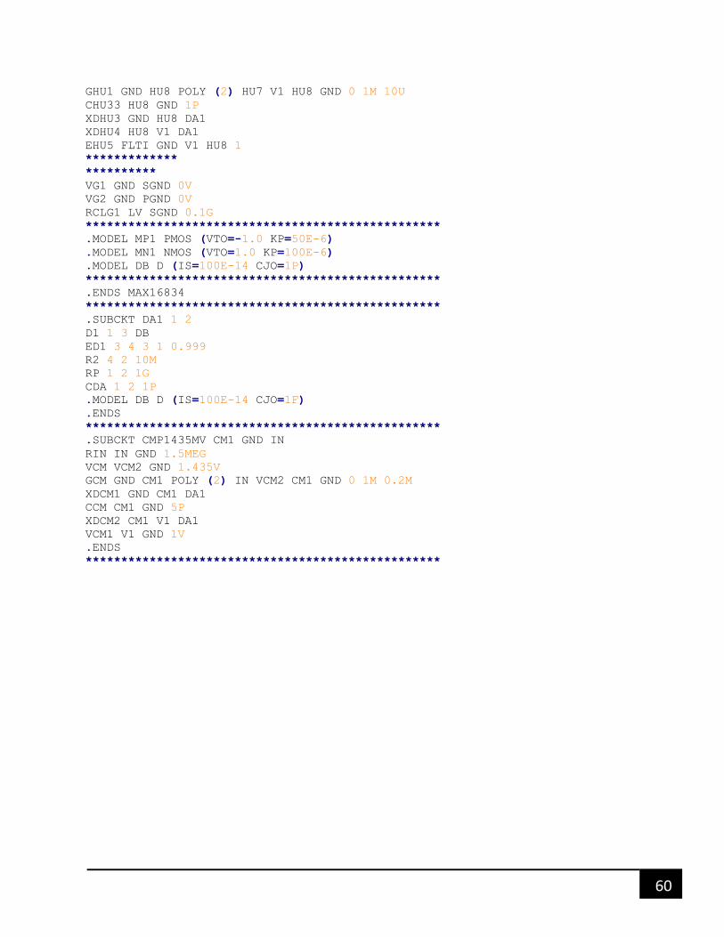
60
GHU1 GND HU8 POLY (2) HU7 V1 HU8 GND 0 1M 10U
CHU33 HU8 GND 1P
XDHU3 GND HU8 DA1
XDHU4 HU8 V1 DA1
EHU5 FLTI GND V1 HU8 1
*************
**********
VG1 GND SGND 0V
VG2 GND PGND 0V
RCLG1 LV SGND 0.1G
**************************************************
.MODEL MP1 PMOS (VTO=-1.0 KP=50E-6)
.MODEL MN1 NMOS (VTO=1.0 KP=100E-6)
.MODEL DB D (IS=100E-14 CJO=1P)
**************************************************
.ENDS MAX16834
**************************************************
.SUBCKT DA1 1 2
D1 1 3 DB
ED1 3 4 3 1 0.999
R2 4 2 10M
RP 1 2 1G
CDA 1 2 1P
.MODEL DB D (IS=100E-14 CJO=1F)
.ENDS
**************************************************
.SUBCKT CMP1435MV CM1 GND IN
RIN IN GND 1.5MEG
VCM VCM2 GND 1.435V
GCM GND CM1 POLY (2) IN VCM2 CM1 GND 0 1M 0.2M
XDCM1 GND CM1 DA1
CCM CM1 GND 5P
XDCM2 CM1 V1 DA1
VCM1 V1 GND 1V
.ENDS
**************************************************

61
*si2318DS MACROMODEL
*March 21, 2005
*Doc. ID: 78869, S-50383, Rev. B
*File Name: Si2318DS_PS.txt and Si2318DS_PS.lib
.SUBCKT Si2318DS 4 1 2
M1 3 1 2 2 NMOS W=854711u L=0.25u
M2 2 1 2 4 PMOS W=854711u L=0.45u
R1 4 3 RTEMP 21E-3
CGS 1 2 420E-12
DBD 2 4 DBD
****************************************************************
.MODEL NMOS NMOS (LEVEL = 3 TOX = 5E-8
+ RS = 11E-3 RD = 0 NSUB = 2.8E17
+ KP = 1.2E-5 UO = 650
+ VMAX = 0 XJ = 5E-7 KAPPA = 1E-2
+ ETA = 1E-4 TPG = 1
+ IS = 0 LD = 0
+ CGSO = 0 CGDO = 0 CGBO = 0
+ NFS = 0.8E12 DELTA = 0.1)
****************************************************************
.MODEL PMOS PMOS (LEVEL = 3 TOX = 5E-8
+NSUB = 2E16 TPG = -1)
****************************************************************
.MODEL DBD D (CJO=150E-12 VJ=0.38 M=0.30
+RS=0.1 FC=0.5 IS=1E-12 TT=5E-8 N=1 BV=40.5)
****************************************************************
.MODEL RTEMP RES (TC1=7E-3 TC2=5.5E-6)
****************************************************************
.ENDS
*ss2p4 MACROMODEL
**********************************
* Copyright: *
* Thomatronik GmbH, Germany *
**********************************
* PSPICE
.subckt ss2p4 1 2
ddio 1 2 legd
dgr 1 2 grd
.model legd d is = 7.07124E-005 n = 1.49383 rs = 0.0453563
+ eg = 0.597561 xti = 1.22745 t_measured = 27
+ cjo = 2.93259E-010 vj = 0.7 m = 0.490878 fc = 0.5
+ tt = 1.4427E-009 bv = 44 ibv = 50 af = 1 kf = 0
.model grd d is = 4.83671E-015 n = 1.15567 rs = 0.0281331
+ eg = 1.79827 xti = 0.491328 t_measured = 27
.ends

62
*CREE X-RE LED MACROMODEL
.MODEL XRE D
+ IS=1E-5
+ N=12.4041
+ RS=.2
+ XTI=45.900
+ EG=2.5000
*LED Driver Project Netlist
* Source DRIVER
X_U1 Y 0 N4 N1 N2 N16547 G N15820 N3 DIM S1 N60929 G1 N14515 VIN
N14515
+ N5 GATE 0 SOURCE MAX16834
C_C5 N14515 0 2.2u TC=0, 0
C_C4 0 N1 0.15u TC=0, 0
C_C2 0 N16547 2400p TC=0, 0
R_R10 0 SOURCE 0.1 TC=0, 0
R_R3 0 N15820 10k TC=0, 0
R_R6 N2 N1 9.1k TC=0, 0
R_R5 0 N2 2.1k TC=0, 0
C_C1 0 VIN 6.8u TC=0, 0
R_R1 N3 VIN 30k TC=0, 0
R_R2 0 N3 13k TC=0, 0
C_C7 N20019 N4 .2u TC=0, 0
R_R7 0 N20019 48.3401 TC=0, 0
C_C6 0 N5 0.47u TC=0, 0
R_R4 Y DRAIN 17.8k TC=0, 0
R_R9 0 Y 1k TC=0, 0
C_C3 0 DRAIN 15u TC=0, 0
V_V1 VIN 0 5Vdc
R_R11 G N1 10k TC=0, 0
R_R8 0 S1 0.07 TC=0, 0
C_C8 0 SOURCE .22u TC=0, 0
X_U2 D1 DRAIN SS2P4
X_Q1 D1 G1 S1 SI2318DS
D_D1 DRAIN N30262 XRE
D_D2 N30262 N30358 XRE
D_D3 N30358 N30456 XRE
D_D4 N30456 LED- XRE
X_Q2 LED- GATE SOURCE SI2318DS
L_L1 VIN D1 10uH
R_R12 N60929 0 1m TC=0, 0
C_C9 DRAIN LED- 100u TC=0, 0
C_C10 DRAIN LED- 100u TC=0, 0
R_R13 DIM N1 10k TC=0,0
R_R14 0 DIM 100k TC=0,0