design of a 60 ghz hybrid mode substrate integrated...
TRANSCRIPT

Thomas Deckmyn
Waveguide Cavity-Backed Antenna ArrayDesign of a 60 GHz Hybrid Mode Substrate Integrated
Academic year 2014-2015Faculty of Engineering and ArchitectureChairman: Prof. dr. ir. Daniël De ZutterDepartment of Information Technology
Master of Science in Electrical EngineeringMaster's dissertation submitted in order to obtain the academic degree of
Counsellors: Ir. Martijn Huynen, Ir. Gert-Jan Stockman, Ir. Sam AgneessensSupervisors: Prof. dr. ir. Dries Vande Ginste, Prof. dr. ir. Johan Bauwelinck


Preface
First and foremost, I would like to express my gratitude towards prof. dr. ir. Dries Vande
Ginste and prof. dr. ir. Johan Bauwelinck for providing me with the opportunity to carry out
this research at the Electromagnetics Group and the INTEC design group of the Department
of Information Technology. I thank Prof. Vande Ginste for sharing his expertise and giving
splendid advice, and for his never-ending positivism and support throughout the entire year. I
am very grateful as well for the insights and encouragements Prof. Bauwelinck offered.
Two people I would like to thank very profoundly are ir. Martijn Huynen and
ir. Gert-Jan Stockman. Their excellent guidance and exhaustive feedback were indispensable up
until the very last minute. Thanks to both of you, you helped pave the way towards a gratifying
conclusion of five years of studies.
Special thanks goes out to ir. Sam Agneessens for the assistance with the design of the hybrid
mode SIW antenna array. His expertise and proficient counseling enabled me to successfully
complete the design.
Ir. Niels Lambrecht deserves special thanks as well, for offering theoretical and practical
advice on more than one front. Furthermore, I appreciate the helping hand that was extended
to me by everyone at the research group, whenever I needed it.
My fellow thesis students Bob Mertens, Alexander Vindelinckx, Kristof Baes, Jorn Marievoet,
Piet Merckx and Enrico Massoni also deserve an acknowledgement. Thank you for the positive
vibe in the thesis room and the pleasant days (and evenings) I have spent there with you all.
I would like to thank my parents for their support throughout the entire period of my studies.
They have always believed in me and supported every choice I made. Without them, I wouldn’t
be where I am today. Lastly, but definitely not least, a special thank you is in order for Bieke
Keysabyl, for providing moral support when it was needed most.
Thomas Deckmyn, May 2015

Admission to Loan
The author gives permission to make this master’s dissertation available for consultation and
to copy parts of this master’s dissertation for personal use. In the case of any other use, the
limitations of the copyright have to be respected, in particular with regard to the obligation to
state expressly the source when quoting results from this master dissertation.
Thomas Deckmyn, May 2015

Design of a 60 GHz Hybrid Mode SubstrateIntegrated Waveguide Cavity-Backed
Antenna Arrayby
Thomas DECKMYN
Master’s Dissertation submitted to obtain the academic degree of
Master of Science in Electrical Engineering
Academic 2014–2015
Promoters: Prof. dr. ir. Dries VANDE GINSTE, Prof. dr. ir. Johan BAUWELINCK
Supervisors: Ir. Martijn HUYNEN, Ir. Gert-Jan STOCKMAN, Ir. Sam AGNEESSENS
Faculty of Engineering and Architecture
Ghent University
Department of Information Technology
Chairman: Prof. dr. ir. Daniel DE ZUTTER
Summary
The goal of this master’s dissertation is to develop a highly compact and integratable antenna
array that operates in the 60 GHz band, whilst maintaining compatibility with standard printed
circuit board manufacturing processes. Two different antenna technologies, i.e., microstrip patch
and Substrate Integrated Waveguide (SIW), are thoroughly analyzed through extensive simu-
lation procedures and measurements. This leads to the formulation of a founded opinion that
SIW is the best suited technology to leverage in the array configuration. Moreover, to en-
hance the impedance bandwidth of the inherently band limited cavity-backed SIW antennas,
a technique based on the excitation of hybrid modes is exploited. The integration aspect of
this dissertation is fortified by selecting a 50 µm flexible substrate material for the design of the
hybrid mode SIW antenna and the array. Although the substrate material is extremely thin, a
fractional impedance bandwidth of 3.6% is achieved. An antenna gain and directivity of 7.2 dBi
and 12.0 dBi, respectively, are obtained by constructing a four-element Uniform Linear Array
(ULA).
Keywords
Hybrid mode substrate integrated waveguide; bandwidth enhancement; antenna array; integra-
tion; flexible substrate

Design of a 60 GHz Hybrid Mode Cavity-BackedSubstrate Integrated Waveguide Antenna Array
Thomas Deckmyn
Supervisors: prof. dr. ir. D. Vande Ginste, prof. dr. ir. J. Bauwelinck, ir. G.-J. Stockman, ir. M. Huynenand dr. ir. S. Agneessens
Abstract— The goal of this master’s dissertation is to develop a highlycompact and integratable antenna array that operates in the 60 GHz band,whilst maintaining compatibility with standard printed circuit board man-ufacturing processes. Two different antenna technologies, i.e., microstrippatch and Substrate Integrated Waveguide (SIW), are thoroughly analyzedthrough extensive simulation procedures and measurements. This leads tothe formulation of a founded opinion that SIW is the best suited technologyto leverage in the array configuration. Moreover, to enhance the impedancebandwidth of the inherently band limited cavity-backed SIW antennas, atechnique based on the excitation of hybrid modes is exploited. The inte-gration aspect of this dissertation is fortified by selecting a 50 µm flexiblesubstrate material for the design of the hybrid mode SIW antenna and thearray. A simulated fractional impedance bandwidth of 3.6% is achieved. Asimulated antenna gain and directivity of 7.2 dBi and 12.0 dBi, respectively,are obtained by constructing a four-element Uniform Linear Array (ULA).
Keywords— Hybrid mode substrate integrated waveguide; bandwidthenhancement; antenna array; integration; flexible substrate
I. INTRODUCTION
NOWADAYS, the omnipresent use and rapid evolution ofelectronic devices puts ever rising demands on the hard-
ware engineer of today. The swift development towards higherbitrates, to satisfy the presently unquenchable mobile user, posesnovel challenges in terms of bandwidth. Moreover, higher oper-ating frequencies are explored, which brings about the addedpredicament of high frequency effects. Paired with the vastminiaturization of high speed electronics, the design task at handbecomes ever more complicated.
This master’s dissertation focuses on the design of a band-width enhanced Substrate Integrated Waveguide (SIW) antennaarray, operating in the 60 GHz band. Hybrid modes are excitedinside the cavity and merged in the desired frequency range, no-tably increasing the impedance bandwidth. The need for minia-turization is tackled by designing the antenna array on extremelythin, i.e., 50 µm and 100 µm, flexible substrate materials.
In this abstract, first, the bandwidth enhancement techniquebased on hybrid modes is discussed (Section II). The designof the hybrid mode cavity-backed SIW antenna is considered inSection III and in Section III-B a Uniform Linear Array (ULA)is constructed utilizing the previously designed antenna ele-ments. Measurement results are presented in Section IV. Con-clusions and future research are discussed in Section V.
II. HYBRID MODE EXCITATION
The limited bandwidth of an SIW antenna can be amelioratedby simultaneously exciting two distinct resonances, i.e., hybridmodes, inside the cavity. By merging these hybrid modes withinthe desired frequency range, the impedance bandwidth is signif-icantly enhanced. The two resonances are, in essence, two dif-
(a)
(b)
Fig. 1. Field distribution in the SIW cavity: (a) Dominant E-field distribution oflower hybrid mode in largest half cavity; (b) Dominant E-field distributionof higher hybrid mode in smallest half cavity [1].
ferent combinations of a TE110 and TE120 mode. By offsettingthe slot from the center of the cavity, two half parts with differ-ent dimensions are created. The lower frequency hybrid modeis dominant in the largest half cavity and is a combination ofa strong TE110 and a weak TE120, as depicted by the E-fielddistributions in Figure 1(a). The total E-field is in phase in bothhalf cavities, but radiation can still be evoked due to the high dif-ference in magnitude. The higher hybrid mode is dominant inthe smallest half part and consists of a strong TE120 and a weakTE110, as illustrated in Figure 1(b). Here, the field is out ofphase in both half parts. A large electric field is present accrossthe slot, hence radiation is generated.
III. DESIGN OF THE HYBRID MODE SIW ANTENNA ARRAY
A. Hybrid Mode SIW Antenna
A general configuration for a hybrid mode SIW antenna isdepicted in Figure 2. The cavity dimensions Lc and Wc aredetermined as such that the resonant frequency of the TE110
is 60 GHz. The length of the slot Ls is much larger than λ2 ,
hence it is non-resonant, and the width Ws tunes the impedancematching to some extent. Here, it is opted for dc,u > dc,l; thehigher frequency hybrid mode is dominant in the lower half partof the cavity.
If dc,u increases, the resonating area of the dominant field ofthe lower hybrid mode is enlarged, hence its resonant frequencydecreases. The area of the weak field of the higher frequency hy-brid mode increases as well, but only causes a minor drop in fre-quency. Hence, the lower hybrid mode decreases in frequency,while the higher hybrid mode remains practically unchanged.This causes an enhancement of the bandwidth.

Ls Ws
dc,l
dc,u
Lc
Wc
Fig. 2. General configuration of a hybrid mode SIW antenna.
After several design iterations and ample optimization, thesimulated reflection coefficient for the design on the 50 µm sub-strate is as presented in Figure 3. Two distinct resonances areperceived at 59.16 GHz and 60.38 GHz. The total impedancebandwidth amounts to 2.2 GHz, which corresponds to a frac-tional bandwidth of 3.6% at 60 GHz.
58 59 60 61 62
0
-5
-10
-15
-20
-25
-30
-35
59.16 GHz 60.38 GHz
2.2 GHz
Frequency [GHz]
|S11|[
dB]
Fig. 3. Simulated reflection coefficient of the designed hybrid mode SIW an-tenna.
B. Uniform Linear Array Configuration
An additional benefit of adopting the SIW technology for thedesign of the antenna array, is the high isolation due to the metal-lic via rows [2]. The array elements can be spaced very closelytogether, without inducing high mutual coupling. The UniformLinear Array (ULA) is constructed using four hybrid mode SIWantennas, while reusing the via wall for adjacent elements. Thesimulated reflection coefficient of the SIW antennas in the ULAconfiguration very closely resembles that of a separate element,as in Figure 3. A simulated antenna gain and directivity of7.2 dBi and 12.0 dBi, respectively, is obtained.
IV. MEASUREMENTS
The fabricated hybrid mode SIW antenna array is depictedin Figure 4. As Uniform Thickness Copper Plating (UTCP) ofthe vias is not feasible for such a small quantity of prototypes,grounding of the top layer is achieved by injecting conductivepaste into the holes. A detailed inspection of the array revealsthat residue of the conductive paste has completely filled the in-sets and part of the slot. Attempts have been made to clear thespillage from both. Still, some remains, as illustrated in Fig-ure 5.
Fig. 4. Fabricated hybrid mode SIW antenna ULA on 100 µm flexible substrate.
Measurements are performed using an N5242A Pro-grammable Network Analyzer (PNA-X) from Keysight Tech-nologies and indicate that a standing wave is present on thefeed network of the array. This implies that the matching atboth ends of the feed structure is poor. The insets procure a50 Ω Grounded Coplanar Waveguide (GCPW) structure that isperfectly matched to the feed line. Taking into account the re-maining spillage of the paste in the slot, it is clear that the di-mensions of the insets have changed, effectively altering theimpedance matching. The electric performance of the paste bywhich the vias are grounded is not precisely known at 60 GHzeither, hence it is plausible that the impedance of the SIW an-tenna elements is changed significantly.
Fig. 5. Detail of fabricated hybrid mode SIW antenna array.
Measurements indicate that the dimensions of the antenna el-ements and 50 Ω microstrip lines are accurate, hence a fabrica-tion inaccuracy is not to blame for the poor matching. The elec-trical parameters of the substrate material are characterized at1 MHz in [3], thus the loss tangent and permittivity could havenotably changed at 60 GHz. This discrepancy is likely to con-

tribute to the deteriorating of the impedance matching. More-over, due to the extremely thin substrate material, the perfor-mance of the press fit of the connector is likely to have dimin-ished; a good connection is not unquestionably ensured.
To gain more insight into the effects at hand, the characteris-tics of a 50 Ω reference microstrip line are measured. To quan-tify the amount of additional losses introduced by the combina-tion of connector and substrate, the power balance of the lineis calculated, i.e., |S11|2 + |S21|2. For a lossless transmissionline structure, this should equal unity, indicating that all incidentpower is either reflected or transmitted. Calculations reveal thatapproximately 70% of the incident power is dissipated. This isdue to losses in the copper and substrate, as well as to radiation.This confirms that it is indeed the combination of connector is-sues and an insufficiently characterized substrate material thatare to blame for the faulty operation of the antenna system.
V. CONCLUSIONS AND FUTURE RESEARCH
A highly compact and integratable hybrid mode cavity-backed SIW antenna array for the 60 GHz band was succesfullydesigned. Bandwidth enhancement was achieved by exploitingthe excitation of hybrid modes inside the SIW cavity. Elevatedgain and directivity was procured by utilizing a four-elementULA configuration. The integration aspect was pushed to theutmost extent by selecting extremely thin substrates for the de-sign.
The insufficient characterization of the flexible substrate at60 GHz and the non-ideal processing of the minute vias wasdetrimental for the operation of the fabricated prototypes. Fu-ture research on this topic could certainly encompass investigat-ing the characteristics of flexible substrates for antenna design at60 GHz. Even research towards the development of novel flexi-ble substrate materials for use in the Extremely High Frequency(EHF) band could be performed.
In future work, the combination of the hybrid mode SIW arraywith very high speed phase shifters can yield the development ofadaptive antenna systems at 60 GHz. This can have applicationsin, e.g., millimeter wave radar detection systems.
REFERENCES
[1] G. Q. Luo and Z. F. Hu and W. J. Li and X. H. Zhang and L. L. Sun and J.F. Zheng, “Bandwidth-Enhanced Low-Profile Cavity-Backed Slot Antennaby Using Hybrid SIW Cavity Modes”, IEEE Transactions on Antennas andPropagation, vol. 60, no. 4, pp. 1698 - 1704, April 2012.
[2] M. Bozzi and A. Georgiadis and K. Wu, “Review of Substrate IntegratedWaveguide Circuits and Antennas”, IET Microwaves, Antennas and Prop-agation, vol. 5, no. 8, pp. 909 - 920, September 2011.
[3] DuPontTM, “DuPontTMPyralux R© AP flexible cir-cuit materials, Technical Datasheet [Online]”, Avail-able: http://www.dupont.com/content/dam/assets/products-and-services/electronic-electrical-materials/assets/PyraluxAPclad DataSheet.pdf.

List of Abbreviations i
List of Abbreviations
ADS Advanced Design System
CST Computer Simulation Technology
DC Direct Current
DSP Digital Signal Processing
EHF Extremely High Frequency
FEM Finite Element Method
GCPW Grounded Coplanar Waveguide
MWS Microwave Studio
PNA-X Programmable Network Analyzer
SHF Super High Frequency
SIW Substrate Integrated Waveguide
SMA Sub-Micron version A
ULA Uniform Linear Array
UTCP Uniform Thickness Copper Plating
UWB Ultra Wideband
WLAN Wireless Local Access Network
WPD Wilkinson Power Divider

CONTENTS ii
Contents
List of Abbreviations i
1 Introduction 1
1.1 High Frequency Design and Challenges . . . . . . . . . . . . . . . . . . . . . . . . 1
1.2 Goal and Outline . . . . . . . . . . . . . . . . . . . . . . . . . . . . . . . . . . . . 2
2 Antenna Design Aspects 3
2.1 Substrate Material . . . . . . . . . . . . . . . . . . . . . . . . . . . . . . . . . . . 3
2.2 Microstrip Patch Antenna . . . . . . . . . . . . . . . . . . . . . . . . . . . . . . . 3
2.2.1 Operating Mechanism . . . . . . . . . . . . . . . . . . . . . . . . . . . . . 4
2.2.2 Impedance Matching . . . . . . . . . . . . . . . . . . . . . . . . . . . . . . 6
2.3 Substrate Integrated Waveguide Technology . . . . . . . . . . . . . . . . . . . . . 7
2.3.1 Operating Mechanism . . . . . . . . . . . . . . . . . . . . . . . . . . . . . 8
2.3.2 Cavity-Backed SIW Antenna . . . . . . . . . . . . . . . . . . . . . . . . . 8
2.4 Simulation Software . . . . . . . . . . . . . . . . . . . . . . . . . . . . . . . . . . 9
3 Deembedding of Connector and Feed Line Structure 10
3.1 Scattering Transfer Parameters . . . . . . . . . . . . . . . . . . . . . . . . . . . . 10
3.2 Deembedding Algorithm Based on Matrix-Pencil Method . . . . . . . . . . . . . 11
3.2.1 Illustrative Example . . . . . . . . . . . . . . . . . . . . . . . . . . . . . . 13
3.3 Characteristics of a Stand Alone Antenna . . . . . . . . . . . . . . . . . . . . . . 14
4 Design and Measurement of Antenna Test Structures 16
4.1 Substrate and Connector . . . . . . . . . . . . . . . . . . . . . . . . . . . . . . . . 16
4.2 Microstrip Patch Antenna . . . . . . . . . . . . . . . . . . . . . . . . . . . . . . . 17
4.2.1 Simulation Results . . . . . . . . . . . . . . . . . . . . . . . . . . . . . . . 18
4.2.2 Corner Analysis . . . . . . . . . . . . . . . . . . . . . . . . . . . . . . . . 18
4.3 Cavity-Backed SIW Antenna . . . . . . . . . . . . . . . . . . . . . . . . . . . . . 21
4.3.1 Simulation Results . . . . . . . . . . . . . . . . . . . . . . . . . . . . . . . 21
4.3.2 Corner Analysis . . . . . . . . . . . . . . . . . . . . . . . . . . . . . . . . 24
4.4 Transmission Line Test Structures for Deembedding . . . . . . . . . . . . . . . . 25
4.5 Measurements . . . . . . . . . . . . . . . . . . . . . . . . . . . . . . . . . . . . . . 26
4.5.1 Microstrip Patch Antenna . . . . . . . . . . . . . . . . . . . . . . . . . . . 27
4.5.2 Cavity-Backed SIW Antenna . . . . . . . . . . . . . . . . . . . . . . . . . 29

CONTENTS iii
4.6 Topology for Antenna Array . . . . . . . . . . . . . . . . . . . . . . . . . . . . . . 31
5 Hybrid Mode SIW Antenna Array 32
5.1 Hybrid Mode Cavity-Backed SIW Antenna . . . . . . . . . . . . . . . . . . . . . 32
5.1.1 Operating Mechanism . . . . . . . . . . . . . . . . . . . . . . . . . . . . . 32
5.1.2 Substrate Material . . . . . . . . . . . . . . . . . . . . . . . . . . . . . . . 33
5.1.3 Design . . . . . . . . . . . . . . . . . . . . . . . . . . . . . . . . . . . . . . 34
5.1.4 Simulation Results . . . . . . . . . . . . . . . . . . . . . . . . . . . . . . . 35
5.2 Uniform Linear Antenna Array . . . . . . . . . . . . . . . . . . . . . . . . . . . . 37
5.3 Array Design . . . . . . . . . . . . . . . . . . . . . . . . . . . . . . . . . . . . . . 38
5.3.1 Mutual Coupling Between Array Elements . . . . . . . . . . . . . . . . . . 39
5.3.2 Simulation Results . . . . . . . . . . . . . . . . . . . . . . . . . . . . . . . 40
5.3.3 Wilkinson Power Divider for Feed Network . . . . . . . . . . . . . . . . . 42
5.3.4 Influence of Feed Network . . . . . . . . . . . . . . . . . . . . . . . . . . . 44
5.4 Measurements . . . . . . . . . . . . . . . . . . . . . . . . . . . . . . . . . . . . . . 45
6 Conclusion and Future Research 49
Bibliography 51
List of Figures 53
List of Tables 56

INTRODUCTION 1
Chapter 1
Introduction
1.1 High Frequency Design and Challenges
The omnipresent use and rapid evolution of electronic devices places ever rising demands on the
hardware engineer of today. Higher bit rates are needed to offer high speed wireless communica-
tion to the presently unquenchable mobile user, which poses many novel challenges in terms of
bandwidth. Moreover, higher operating frequencies make that high frequency effects come into
play and the design task at hand becomes severely more complicated. The hardware engineer
needs to be fully aware of these effects, which are among others more pronounced parasitic
effects, rising losses with frequency and wave phenomena in interconnection structures.
A second trend is the vast miniaturization of high speed electronics. Hence, compact and easily
integrated antenna systems are of prime interest. Antennas rapidly scale down with rising
frequency, but need to be manufactured with high accuracy to ensure proper millimeter wave
operation. They need to remain low-cost as well, if they are to be used in high volume consumer
applications. This evidently puts a strain on the available manufacturing processes and a proper
design needs to be robust against possible inaccuracies.
If the dimensions of planar electronic structures become electrically large, i.e., of the order of
a wavelength of operation, distributed circuit analysis needs to be performed. Transmission
line effects set in and the characteristic impedance of lines becomes an important parameter.
An discontinuity in the impedance of the signal line will introduce reflections and will result in
additional attenuation. As losses are already strongly present at high frequencies, impedance
matching requires additional attention.
In this master’s dissertation, antenna designs in the Super High Frequency (SHF) and Extremely
High Frequency (EHF) range are performed, hence the high frequency effects mentioned above
are taken into close consideration.

INTRODUCTION 2
1.2 Goal and Outline
The goal of this master’s dissertation is to design a highly compact and easily integrated antenna
array that operates in the unlicensed 60 GHz band [1]. A hybrid mode technique will be used
to enhance the bandwidth, while the array configuration will enable beam forming and yield
elevated gain.
To arrive at a 60 GHz antenna array with optimal performance in the final stage of the design,
a first step is to develop test structures to assess the inherent advantages and disadvantages
of different antenna technologies at various frequencies. By comparing the simulations and
measurements at distinct frequencies, it can be deduced which effects are more severe at higher
frequencies. Concretely, both the microstrip patch and Substrate Integrated Waveguide (SIW)
antenna technology will be exploited to design radiating elements with resonant frequencies
at 15 GHz, 30 GHz and 60 GHz. After manufacturing, intensive measurements will enable a
comparison of both topologies and will provide sufficient arguments to make an appropriate
choice of topology. Moreover, any critical steps in the manufacturing process can be exposed as
the dimensions of the devices miniaturize with rising frequency.
In Chapter 2 the microstrip patch antenna and SIW technologies will be addressed in a theoret-
ical manner. In Chapter 3 a method to eliminate the effects of a connector from S-parameter
measurements will be introduced. The design and measurement of the antenna test structures
is described in Chapter 4, and a reasoned choice of the most suitable technology for this appli-
cation will be made as well. In Chapter 5, the concept of hybrid modes will be introduced and
the array will be designed. Lastly, in Chapter 6 conclusions will be provided and future research
will be considered as well.

ANTENNA DESIGN ASPECTS 3
Chapter 2
Antenna Design Aspects
2.1 Substrate Material
Selecting the best suitable substrate for an antenna is of the utmost importance. By opting for
a proper material, the inherent restrictions of the antenna, such as insertion loss, narrowband
behavior and low efficiency can be ameliorated. The parameters of the substrate, i.e., the relative
dielectric permittivity εr and loss tangent tan δ, have notable effects on the performance of the
device. A high loss tangent implies strong losses in the substrate material, which will result in a
low radiation efficiency. The permittivity determines the speed of wave propagation inside the
material. A high permittivity results in slower propagation and thus a decreased wavelength.
This can be used in antenna miniaturization; if an antenna is placed in a medium with higher
permittivity, the required size for half wavelength resonance decreases and the antenna will be
smaller. Unfortunately, a high permittivity diminishes the available bandwidth.
Another important parameter is the thickness of the substrate material. The ohmic losses in
the copper of a microstrip line, due to the finite conductivity of the conductor, are proportional
to the height of the substrate and inversely proportional to the width of the line [2]. A thin
substrate hence decreases ohmic losses, but it also degrades the radiation efficiency and band-
width of a patch antenna for example. If the substrate material is thick, a larger bandwidth
and more efficiency can be achieved, but the propagation of surface waves will be enhanced.
The fundamental order surface wave has a cut off frequency at Direct Current (DC), but higher
order surface modes will be excited if the substrate thickness is too large [3] [4]. These waves
travel inside the substrate and are scattered at surface discontinuities, degrading the radiation
pattern and polarization characteristics of the antenna. Moreover, the power that is used to
excite these waves, can no longer be radiated, hence the radiation efficiency is degraded as well.
2.2 Microstrip Patch Antenna
Microstrip patch antennas have the advantage of being low-profile and light weight, and can
easily be integrated together with other planar circuits. A patch antenna consists of a metallic

ANTENNA DESIGN ASPECTS 4
film bonded to a grounded dielectric substrate. The thickness of the substrate layer and the
relative permittivity εr are usually small, hence the patch behaves more like a parallel plate
transmission line. If the patch is fed using a microstrip feed line, as depicted in Figure 2.1,
waves travel from the feed point to the edges of the patch. There, a discontinuity is present
and the fields sense an open circuit, hence a considerable amount of reflections occur. This
suggests that the portion of incident energy that is radiated, is reduced; this in turn leads to
the assumption that a patch antenna can be seen as a resonant (leaky) cavity. The fact that a
patch antenna behaves more like a cavity supports the known limitations of this topology, i.e.,
low efficiency and narrowband behavior.
x
y
z
εr
h
L
W
Figure 2.1: Simple microstrip patch antenna configuration.
2.2.1 Operating Mechanism
A simple microstrip patch configuration is presented in Figure 2.1, with W and L the width
and length of the patch respectively. The substrate material is characterized by its relative
permittivity εr and height h. The radiation mechanism of the microstrip patch antenna is
discussed using a simple aperture model. Typically, the height of the substrate is a small
fraction of the wavelength (order of λ20) and the length L is of the order of λ
2 . As the height h of
the cavity is very small (h λ, with λ the wavelength inside the dielectric material), the fields
are assumed constant with respect to the z-axis. The radiation is caused by the fringing E-fields
emerging from the exposed substrate at the edge of the patch, as depicted in Figure 2.2.

ANTENNA DESIGN ASPECTS 5
x
z
yL
Fringing fields
εr
Figure 2.2: Fringing E-fields as radiation mechanism for a patch antenna.
Applying the cavity model to the patch antenna topology in Figure 2.1, yields that the resonant
frequency (fr)mnp of the transverse magnetic TMmnp mode [5] is given by
(fr)mnp =c
2π√εr
√(mπh
)2+(nπL
)2+(pπW
)2, (2.1)
with εr the relative permittivity of the substrate material and c the speed of light in vacuum.
The fundamentel order mode, i.e., the lowest in frequency, now depends on the dimensions of
the patch. If L > W h holds, the fundamental mode is the TM010. It follows from (2.1) that
its resonant frequency is given by
(fr)010 =c
2L√εr. (2.2)
A practical width of the patch that yields good radiation efficiencies is [5]
W =c
2fr
√2
εr + 1. (2.3)
When alternatively W > L h, the fundamental mode is the TM001 with resonant frequency
given by
(fr)001 =c
2W√εr. (2.4)
Equivalently, a practical length that yields good radiation efficiency is
L =c
2fr
√2
εr + 1. (2.5)
As stated above, fringing fields are the sources of radiation for the microstrip patch antenna.
From Figure 2.2 one can observe that most field lines of the electric field reside inside the
substrate, but some of the field lines exist in the air. Because some of the lines travel through
the air surrounding the substrate, the fields feel an effective dielectric constant εr,eff that differs

ANTENNA DESIGN ASPECTS 6
from the εr of the substrate itself. The low frequency value for the effective relative permittivity
εr,eff is given by [6]
εr,eff =
εr+1
2 + εr−12
[1 + 12 h
W
]− 12 , L > W h
εr+12 + εr−1
2
[1 + 12 hL
]− 12 , W > L h
. (2.6)
For higher frequencies the effective dielectric constant starts to increase monotonically with fre-
quency, approaching the dielectric constant of the substrate.
Due to the fringing of the fields the patch is electrically wider and longer as compared to its
physical dimensions, hence this needs to be accounted for in the calculation of the resonant
frequency. A commonly used approximate expression for the increase in length is [7]
∆L = 0.412h(εr,eff + 0.3)
(Wh + 0.264
)(εr,eff − 0.258)
(Wh + 0.8
) . (2.7)
This yields an effective electrical length Leff = L + 2∆L and a resonant frequency for the
dominant TM010 mode given by
(fr)010 =c
2(L+ 2∆L)√εr
=c
2Leff√εr. (2.8)
Equivalently, an effective width Weff can be calculated and used to obtain the resonant frequency
of the TM001 mode.
2.2.2 Impedance Matching
The designed patch antenna will be excited using a 50 Ω microstrip feed line, as already depicted
in Figure 2.1. To avoid high reflections at the junction between patch and feed line, the edge
impedance of the antenna has to be matched to the 50 Ω of the microstrip line. The impedance
at the edge of the patch [8] is, in good approximation, given by
Zin = 90ε2r
ε2r − 1
(L
W
)2
Ω. (2.9)
As is clear, the edge impedance of the antenna can be set to 50 Ω by calculating the appropriate
value for the width W .
A different technique, and of most practical importance, makes use of insets to perform the
matching, as presented in Figure 2.3. The input impedance seen at the edge depends on the
inset depth R as defined in
Z ′in(R) = cos2
(πR
L
)Zin, (2.10)

ANTENNA DESIGN ASPECTS 7
where Zin can be calculated using (2.9). It can be understood from (2.10) that the input
impedance exhibits a maximum value for R = 0 and decreases monotonically with increasing
depth R, until the minimum value is reached for R = L2 . In the center of the patch the voltage
is zero and the current is maximum, hence the impedance is zero. The width of the inset d can
be used to further tune the resonant input impedance.
L
W
R
d
Figure 2.3: Microstrip patch antenna with insets for impedance matching.
2.3 Substrate Integrated Waveguide Technology
SIWs are planarly integrated structures with a close resemblance to conventional rectangular
waveguides. SIWs are fabricated by connecting two parallel copper planes with electrically con-
ductive vias embedded in the substrate, as illustrated in Figure 2.4. Hence, this technology
allows one to integrate a usually non-planar rectangular waveguide, while maintaining compat-
ibility with conventional planar printed circuit board processing steps. Because of the high
resemblance to rectangular waveguides, SIW structures also exhibit the main advantages of
having a high Q-factor and high electrical shielding. This technology creates the possibility to
integrate passive and active components, and even antennas, onto the same substrate, which is
of prime practical interest.
sd
w
Figure 2.4: SIW structure: conductive vias connecting parallel copper planes.

ANTENNA DESIGN ASPECTS 8
2.3.1 Operating Mechanism
As stated above, SIWs closely resemble conventional rectangular waveguides, be it in planar
form, but SIW structures also display similar propagation characteristics. The guided modes
are practically equal to the TEn0-modes that propagate in a rectangular waveguide with similar
dimensions, where the dominant mode is TE10. Due to this high similarity, empirical formulas
have been presented that allow one to obtain the effective width weff of a rectangular waveguide
with the same propagation characteristics as the SIW structure. It holds that [9]
weff = w − d2
0.95s, (2.11)
where d and s are the diameter of the vias and the spacing between the vias respectively. The
frequency of the first order guided mode in an SIW structure can be obtained as the frequency
of the TE10 guided mode in a rectangular waveguide of width weff, and hence equals [3]
f10 =c
2√εrweff
(2.12)
=c
2√εr
(w − d2
0.95s
)−1
. (2.13)
The similarity only holds provided that the radiation leakage through the gaps between the
vias is neglegible, i.e., the row of vias needs to approximate a contiguous metallic wall at the
operating frequency. If this is the case, the SIW structure can be treated as being a rectangular
waveguide with width weff as defined in (2.11). Empirical constraints on the dimensions of and
the spacing between the vias such that radiation leakage is neglegible, have been formulated
in [10] as
s ≤ 2d
d ≤ λ10 ,
(2.14)
with λ the wavelength in the substrate material.
2.3.2 Cavity-Backed SIW Antenna
A cavity-backed SIW antenna consists of a cavity resonator constructed in SIW technology. If
the cavity is made leaky by introducing one or more slots, radiation occurs. The cavity is built
up as depicted in Figure 2.5 and is excited using a microstrip feed line. The resonant frequency
of the TEmn0-mode can be found as [11]
fmn0 =c√
2πεr
√(mπ
Weff
)2
+
(nπ
Leff
)2
, (2.15)
where Leff and Weff can be obtained using (2.11), c is the speed of light in vacuum and εr is the
relative permittivity of the substrate material. As this is an empirical expression, tuning will

ANTENNA DESIGN ASPECTS 9
be necessary to obtain the desired operating frequency. Note that the restrictions on the via
spacing and diameter (2.14) need to be fulfilled to ensure proper operation.
LW
Ls WsRgcpw
dgcpw
Figure 2.5: SIW resonant cavity with microstrip line feed.
Once the cavity is constructed at the right resonant frequency, a slot is added to evoke radiation.
The slot can be etched in the ground plane, which will isolate the radiation caused by the feeding
network from the desired radiation coming from the slot, or it can be etched in the top copper
plane, which will drastically lower backward radiation.
The slot is an important tuning element of the cavity-backed SIW antenna. As described in [12],
the width Ws can be tuned to obtain optimal impedance bandwidth, but the effect on impedance
bandwidth is much less than that of the substrate thickness. The length of the slot Ls can be
used to adjust the resonant frequency by some degree, but the resonance is primarily determined
by the cavity size. The length of the slot also has major influence on the radiation efficiency,
which is at its maximum when the slot length is half a wavelength.
To match the edge impedance of the cavity to the 50 Ω microstrip feed line, the parameters
Rgcpw and dgcpw need to be chosen such that a 50 Ω grounded coplanar waveguide (GCPW)
structure is obtained.
2.4 Simulation Software
When designing millimeter wave antenna systems, one wants to predict the real behaviour of the
device as accurately as possible. A good simulation tool that takes into account all high frequency
effects is thus indispensable. For all designs that follow, the Keysight Technologies Advanced
Design System (ADS) simulation software is used. It incorporates a planar 3D electromagnetic
solver Momentum, which uses a frequency-domain Method of Moments (MoM) to simulate
complete board structures whilst taking parasitic effects, losses and coupling into account.

DEEMBEDDING OF CONNECTOR AND FEED LINE STRUCTURE 10
Chapter 3
Deembedding of Connector and Feed
Line Structure
To connect the antenna test structures that will be designed in the next chapter to measurement
equipment or an exterior circuit, a suitable connector will be needed, i.e. one with excellent high
frequency performance. Still, this connector will introduce a certain amount of reflections, due
to impedance mismatch and insertion loss. In this chapter a method is discussed that enables
extracting the S-parameters of the connector from a series of reference measurements. These
extracted characteristics can then be deembedded from the measured characteristics of the
cascade of connector and antenna, eliminating the added losses and reflections.
3.1 Scattering Transfer Parameters
A different approach to represent the characteristics of a two-port network is by means of T-
parameters [13] (Scattering Transfer Parameters). These are an alternative to the well-known
S-parameters with their prime advantage being cascadeability. The T-parameters relate the
amplitudes of the waves a1 and b1 at the input of the two-port to the amplitudes of the waves
a2 and b2 at the output (see Figure 3.1), while the S-parameters relate the amplitudes of the
reflected waves at both input and output, i.e. b1 and b2, to the incident waves a1 and a2. The
T-parameters are hence defined by the relation
(a1
b1
)=
(T11 T12
T21 T22
)·(b2
a2
). (3.1)
The corresponding T-parameters can be calculated from the two-port’s S-parameters using the

DEEMBEDDING OF CONNECTOR AND FEED LINE STRUCTURE 11
following conversion formulas [14].
T11 = 1
S21
T12 = −S22S21
T21 = S11S21
T22 = −S11S22−S12S21S21
.
(3.2)
As stated above, the main advantage of T-parameters over S-parameters is cascadeability. To
illustrate this, consider a two-port network that consists of 2 two-port networks in a cascade
configuration as depicted in Figure 3.1.
a1
b1
a2
b2
a3
b3
a4
b4
T 1 T 2
Figure 3.1: Cascade of two arbitrary two-port networks.
Taking into account (3.1), it holds for the network of Figure 3.1 that(a1
b1
)=
(T 1
11 T 112
T 121 T 1
22
)·(b2
a2
)(3.3)
and (a3
b3
)=
(T 2
11 T 212
T 221 T 2
22
)·(b4
a4
). (3.4)
It now follows that the scattering transfer matrix for the overall network is defined as the matrix
product of the T-matrices of the cascaded two-port networks [14], i.e.(a1
b1
)=
(T 1
11 T 112
T 121 T 1
22
)·(T 2
11 T 212
T 221 T 2
22
)·(b4
a4
). (3.5)
The previous reasoning can be extended to an arbitrary cascade of N two-port networks, yielding
an expression for the overall scattering transfer matrix T given by
T = T 1 · T 2 · ... · TN . (3.6)
3.2 Deembedding Algorithm Based on Matrix-Pencil Method
As mentioned above, a deembedding algorithm will be used to extract the characteristics of
the connector with simple reference measurements as a starting point. A novel matrix-pencil
two-line method that achieves this was developed in [15], where it was exerted to eliminate the
impact of the connector in performing substrate characterization for wearable antenna systems.

DEEMBEDDING OF CONNECTOR AND FEED LINE STRUCTURE 12
To achieve deembedding, the S-parameters of two microstrip lines of length l1 and l2, with
l2 > l1, as depicted in Figure 3.2, need to be measured. The characteristics of the connectors,
in cascade with a coax-to-microstrip transition, are defined by SA and SB. The piece of ideal
lossy transmission line, with length ∆L = l2 − l1, is defined by SL. The two lines are fully
characterized by their propagation factor γ and characteristic impedance Z0. Prior knowledge
of the impedance Z0 is obsolete as the effects of impedance mismatch are included in the model.
l1
SA SB
l2
SA SBSL
Figure 3.2: Microstrip lines with coax-to-microstrip transitions SA and SB and ideal lossy
transmission line section SL.
Defining the scattering transfer matrix of the short line, with length l1, as T short and the matrix
of the long line, with length l2, as T long one can express both matrices as [15]
T short = TA · TBT long = TA · TL · TB.
(3.7)
Here TA, TB and TL are the T-parameter equivalents of SA, SB and SL respectively, which can
be obtained using the conversion formulas (3.2). If (3.7) is solved, one obtains
T · TA = TA · TL, (3.8)
where T = T long · T−1
short · T long. The S-parameter matrices Slong and Sshort can be obtained
through measurements of both microstrip lines and converted to their T-parameter counterparts
using conversion formulas [13].
The method described in [15] calculates the deembedded complex propagation factor γ of the
piece of transmission line defined by TL based on an eigenvalue equation obtained from (3.8).
Perturbations in the complex propagation constant can yield unphysical results, hence they are
minimized by using the matrix-pencil method as an averaging method. Once the propagation
constant γ is obtained, the scattering transfer parameters TA and TB (corresponding to the coax-
to-microstrip transitions SA and SB respectively) are constructed, hence the characteristics of
the connector are extracted.
It can be seen from Figure 3.2 that the extracted characteristics TA in reality comprise the
characteristics of the connector in cascade with a coax-to-microstrip transition and a piece of

DEEMBEDDING OF CONNECTOR AND FEED LINE STRUCTURE 13
transmission line of length lA = 0.5l1. If a suitable choice is made for the lengths of the reference
microstrip lines, not only the influence of the connector, but of the entire feed line exciting
the microstrip patch antenna in Figure 2.1 can be eliminated as well. This implies that after
measurements of the return loss of the fabricated antennas, the additional losses due to connector
as well as feed line can be removed from the measurements, yielding the characteristics of the
stand-alone antenna. How the characteristics of connector and feedline will be deembedded from
the antenna measurements in a later stage of the design is discussed in Section 3.3.
3.2.1 Illustrative Example
To prove the correctness of the deembedding algorithm presented in Section 3.2, an illustrative
example based on simulations will be given. All simulations are performed using the Keysight
Technologies ADS circuit solver. The algorithm will be used to extract the characteristics of
a connector with T-matrix T conn, which is modeled as a 35 Ω discontinuity in a piece of 50 Ωtransmission line. For this example, a 50 Ω transmission line with a 35 Ω discontinuity at each
side is considered (see Figure 3.3), which corresponds to a transmission line with connectors at
both ends. As discussed in Section 3.2 the S-parameters of two microstrip lines with different
lengths need to be simulated and fed to the deembedding algorithm.
35 Ω TL 50 Ω TL 35 Ω TL
50 ΩVs,1
Port plane
50 Ω
Port plane
Vs,2
Figure 3.3: Piece of 50 Ω transmission line with connector modeled as 35 Ω discontinuity.
To assess the correctness of the algorithm, a second S-parameter simulation is performed solely
on the connector as pictured in Figure 3.4. Now the characteristics of the connector simulated
by the circuit solver can be compared to the result of the deembedding algorithm, as presented
in Figure 3.5. It can be seen that the algorithm yields results that correspond very well to what
is predicted by the simulation.
35 Ω TL
50 ΩVs,1
Port plane
50 Ω
Port plane
Vs,2
Figure 3.4: S-parameter simulation performed on modeled connector.

DEEMBEDDING OF CONNECTOR AND FEED LINE STRUCTURE 14
0 10 20 30 40 50 60
−50
−40
−30
−20
−10
Frequency [GHz]
S11
[dB
]
Figure 3.5: Characteristic of model connector: extracted with deembedding algorithm (solid
line) and simulated with circuit solver (dashed line).
3.3 Characteristics of a Stand Alone Antenna
As the S-parameters of the connector and the piece of feed line are extracted as described in
the previous section, these can now be used to calculate the characteristics of the stand-alone
antenna from the S-parameter measurement of the cascade of connector, feed line and antenna.
As stated, the S-parameter measurements are performed on the system as depicted in Figure
3.6, where a1,2 and b1,2 are incident and reflected power waves respectively.
50 ΩVs
Port plane
a1
b1
a2
b2
Connector
Figure 3.6: Block diagram of measurement to be performed.
For this system it is known that
(b1
a1
)= T conn
(a2
b2
), (3.9)
where T conn is the T-matrix (containing the two-port Scattering Transfer Parameters) of the
connector, which is fully known as a result of the deembedding algorithm. The system in

DEEMBEDDING OF CONNECTOR AND FEED LINE STRUCTURE 15
Figure 3.6 is a one-port, hence the conducted measurement will yield a reflection coefficient Sm,
with
Sm =b1a1. (3.10)
If one wants to retrieve the return loss of the stand-alone antenna, the S-parameter Sa needs to
be extracted, which is defined as
Sa =a2
b2. (3.11)
Combining (3.9) and (3.11) one obtains
(b1
a1
)= T conn
(Sab2
b2
), (3.12)
and evidently
(Sa
1
)b2 = T
−1
conn
(b1
a1
). (3.13)
If one defines the matrix X as the inverse matrix of T conn, the system of equations
Sab2 = X11b1 +X12a1
b2 = X21b1 +X22a1
(3.14)
becomes apparent and provides an expression for the return loss of the antenna, given by
Sa =X11
b1a1
+X12
X21b1a1
+X22
. (3.15)
Taking into account (3.10) the return loss of the antenna can be expressed as a function of the
measured S-parameter Sm of the system defined in Figure 3.6 and the characteristics of the
connector obtained with the deembedding algorithm. One obtains
Sa =X11Sm +X12
X21Sm +X22, (3.16)
with X = T−1
conn.
It is clear that this method enables one to calculate the characteristics of the stand-alone antenna,
eliminating all added losses and reflections due to the presence of the feed line and connector.

DESIGN AND MEASUREMENT OF ANTENNA TEST STRUCTURES 16
Chapter 4
Design and Measurement of Antenna
Test Structures
4.1 Substrate and Connector
The substrate selected for the design and fabrication of the antenna test structures is the
RO4350B® Rogers Corporation high speed laminate [16]. It offers superior high frequency
performance and is compatible with standard low-cost circuit fabrication techniques. The main
benefits are the low dielectric loss and the stability of the dielectric constant over a broad fre-
quency range. The latter makes this laminate an ideal material for broadband applications. The
main characteristics are summarized in Table 4.1.
εr 3.48 (10 GHz)
tan δ 0.0037 (10 GHz)
thickness 168 µm
Cu thickness 35 µm
Table 4.1: Characteristics of Rogers RO4350B High Speed Laminate.
The connectors that will be used to measure the antenna test structures are 1.85 mm Sub-Micron
version A (SMA) end launch connector assemblies fabricated by Southwest Microwave [17] (Fig-
ure 4.1), which are suited for applications up to 67 GHz. A press fit is used to ensure good
connection between connector pin and circuit board, so no soldering is needed. To obtain con-
sistent measurements, the amount of force by which the connector is pressed onto the circuit
board, is controlled with a torque wrench. The end launch connectors are rather bulky and
made out of solid metal, so as a precaution not to interfere with the proper operation of the
antennas, the connector needs to be at a reasonable distance. This implies a long microstrip
feed line towards the patches. An optimized connector footprint will be used as suggested in [18]
and depicted in Figure 4.2. This footprint uses a 50 Ω Grounded Coplanar Waveguide (GCPW)
launch structure to improve the performance of the microstrip and the line is slightly tapered
to match the connector pin.

DESIGN AND MEASUREMENT OF ANTENNA TEST STRUCTURES 17
Figure 4.1: Southwest Microwave 1.85 mm end launch connector.
2.82 mm
280 µm
210 µm
Figure 4.2: Connector footprint with GCPW launch structure.
4.2 Microstrip Patch Antenna
The first step in designing the patch antenna test structures at 15 GHz, 30 GHz and 60 GHz is
using (2.5) to calculate a length L of the patch that yields good radiation efficiencies, with the
desired resonant frequency as a starting point. From this the effective relative permittivity εr,eff
can be determined with (2.6). Once the length L and εr,eff are known, the width extension ∆W
can be obtained using (2.7), where in this case W must be replaced with L. Taking into account
all of the above, the physical width W that will yield the desired resonant frequency for the
TM001-mode is obtained by solving
W =1
2fr√εr,eff√ε0µ0
− 2∆W. (4.1)
The last step is adding insets to obtain good impedance matching to the 50 Ω feed line. The
depth R of the inset, as defined in Figure 2.3, is calculated using (2.10).
After several design iterations, including extensive optimization steps, the final designs for the
patch antenna test structures have dimensions as listed in Table 4.2.

DESIGN AND MEASUREMENT OF ANTENNA TEST STRUCTURES 18
15 GHz 30 GHz 60 GHz
W [mm] 5.95 2.70 1.50
L [mm] 5.21 2.60 1.28
R [mm] 1.83 0.94 0.43
d [mm] 0.20 0.20 0.16
Lfeed [mm] 10.75 10.75 10.75
Table 4.2: Dimensions of designed microstrip patch antenna test structures.
4.2.1 Simulation Results
All simulation results presented below include substrate and copper losses. The simulated re-
flection coefficientes for the designed antennas are depicted in Figure 4.3. As can be seen, all
designs exhibit a well defined resonance peak at the desired frequency. However, there are dis-
tinct differences between the characteristics of the three antennas. The patch antenna at 60 GHz
(Figure 4.3(c)) exhibits much more insertion loss than the one at 15 GHz (Figure 4.3(c)). The
higher insertion loss is to be expected as the attenuation due to both conductor and substrate
losses increases with frequency [3]. The limited bandwidth, which is an inherent disadvantage
of microstrip patch technology, is clearly visible as well. The antennas at 15 GHz, 30 GHz and
60 GHz have a relative impedance bandwidth of 1.2%, 1.8% and 3.5%, respectively.
The simulated directivity and gain in the E-plane are presented in Figure 4.4. The gain is lower
than the directivity in all three cases, because of the substantial losses at these high frequencies.
Directivity is related to gain as [19]
G(θ, φ) =D(θ, φ)
KL, (4.2)
where KL is a real factor, greater than unity and independent of direction, that represents the
power losses in the materials forming the antenna. The radiation efficiency is defined as the
ratio of the gain to the directivity, hence it is equal to 1KL
. As is clear from Figure 4.4, the
efficiency of the three patches is moderate; there is a notable difference between directivity and
gain. The radiation efficiency for all three designs is approximately 60%.
4.2.2 Corner Analysis
As discussed in Chapter 1, the ongoing desire for higher operating frequencies causes a vast
miniaturization of antenna structures and in turn puts a strain on the fabrication processes at
hand. The etching of the antennas will not be infinitely precise, hence an insight into the effects
of possible fabrication flaws is imperative. Consulting Table 4.2, it is clear that the performance
of the patch antenna at 60 GHz is the most sensitive to fabrication inaccuracies because of its
very small dimensions (order of 1 mm). The minimum feature size of the fabrication process is
200 µm and a worst case scenario of a 10% fabrication error is assumed, i.e., a fault of 20 µm.
The dominant mode of the patch antenna at 60 GHz is the TM001 and is determined by the

DESIGN AND MEASUREMENT OF ANTENNA TEST STRUCTURES 19
14 14.5 15 15.5 16
0
-5
-10
-15
-20
-25
170 MHz
Frequency [GHz]
|S11|[
dB
]
(a)
29 29.5 30 30.5 31
0
-5
-10
-15
-20
-25
-30
540 MHz
Frequency [GHz]
|S11|[
dB
]
(b)
58 59 60 61 62
0
-10
-20
-30
2.1 GHz
Frequency [GHz]
|S11|[
dB
]
(c)
Figure 4.3: Simulated reflection coefficient for patch antenna test structures: (a) at 15 GHz; (b)
at 30 GHz and (c) at 60 GHz.
width W (see Table 4.2). Figure 4.5(a) illustrates the effects of the fabrication error on the
resonant frequency of the antenna. Another important feature is the amount of matching, as
it determines the quantity of power that is reflected and thus not radiated. This is mainly
determined by the inset depth R, for which the effects of the fabrication error are depicted
in Figure 4.5(b). It is clear that the most critical parameter is the width of the patch, as it
determines the resonant frequency. An error of 20 µm already causes a notable shift of the
resonance.

DESIGN AND MEASUREMENT OF ANTENNA TEST STRUCTURES 20
−15
−10
−5
0
5
10 dBi
90o
60o
30o
0o
−30o
−60o
−90o
(a)
−15
−10
−5
0
5
10 dBi
90o
60o
30o
0o
−30o
−60o
−90o
(b)
−15
−10
−5
0
5
10 dBi
90o
60o
30o
0o
−30o
−60o
−90o
(c)
Figure 4.4: Simulated directivity (solid) and gain (dotted) in the E-plane of the antenna: (a) at
15 GHz, (b) at 30 GHz and (c) at 60 GHz.
58 59 60 61 62
0
-10
-20
-30
-40
Frequency [GHz]
|S11|[
dB
]
W − 20 µmW + 20 µm
Final Design
(a)
58 59 60 61 62
0
-10
-20
-30
-40
Frequency [GHz]
|S11|[
dB
]
R− 20 µmR+ 20 µm
Final Design
(b)
Figure 4.5: Effect of a 20 µm fabrication error on the 60 GHz patch: (a) error on W affects the
resonant frequency; (b) error on R affects the matching.

DESIGN AND MEASUREMENT OF ANTENNA TEST STRUCTURES 21
4.3 Cavity-Backed SIW Antenna
As stated in Section 2.3, the equivalency between rectangular waveguides and SIW structures
only holds when the restrictions on the via diameter and spacing (2.14) are met. Sizing the vias
is an obligatory first step to ensure proper operation of the SIW antenna. These restrictions
are empirical, hence it is good practice to stay well below these limits. This will make sure the
via wall approximates a continuous conductive wall as good as possible. Table 4.3 summarizes
the via diameter and spacing maxima for each frequency, as well as the values that will be used
during the design. The dimensions at 30 GHz and 60 GHz are the minimal dimensions that still
comply with the fabrication design rules.
f [GHz] dmax [mm] smax [mm] d [mm] s [mm]
15 1.05 2.1 0.5 1
30 0.52 1.04 0.2 0.4
60 0.26 0.52 0.2 0.4
Table 4.3: Via diameter and spacing maxima for SIW operation.
Now, one can start dimensioning the actual cavity-backed SIW antenna as depicted in Figure 2.5.
Firstly, the dimensions of the cavity that correspond to the desired resonant frequency need to
be determined. The slot divides the SIW cavity into two half cavities with equal dimensions
and the radiation is caused by a strong TE120 resonance [20]. The SIW cavities of the antenna
test structures are hence designed to support a TE120 resonance at their desired frequencies of
operation.
From (2.15) the effective widths Weff and lengths Leff of the rectangular waveguides that are
equivalent to the SIW cavities can be determined. Together with the dimensions of the via
diameter and spacing from Table 4.3, the physical dimensions W and L of the SIW cavities can
be calculated using (2.11).
Next, the slot is added in the top copper plane to procure radiation. The slot is resonant to
ameliorate the radiation efficiency to the utmost extent [20], hence it has a length Ls approxi-
mately equal to half a wavelength at the desired operating frequency. The width of the slot Ws is
optimized to slightly improve the impedance bandwidth. Ideal impedance matching is acquired
through dimensioning Rgcpw and dgcpw for a 50 Ω Grounded Coplanar Waveguide (GCPW) feed.
After a considerable number of design iterations and ample optimization, the final dimensions
for the cavity-backed SIW antennas at 15 GHz, 30 GHz and 60 GHz are obtained as given in
Table 4.4.
4.3.1 Simulation Results
The simulated reflection coefficients for the cavity-backed SIW antennas are presented in Fig-
ure 4.6. It is clear that all three designs exhibit a well-defined resonance at the desired frequency.

DESIGN AND MEASUREMENT OF ANTENNA TEST STRUCTURES 22
15 GHz 30 GHz 60 GHz
L [mm] 8.00 4.00 2.00
W [mm] 10.00 4.40 2.40
Ls [mm] 5.82 3.05 1.59
Ws [mm] 0.76 0.30 0.21
Rgcpw [mm] 1.98 1.07 0.62
dgcpw [mm] 0.70 0.32 0.21
Table 4.4: Dimensions of designed cavity-backed SIW antenna test structures.
14 14.5 15 15.5 16
0
-5
-10
-15
-20
-25
-30
-35
-40
130 MHz
Frequency [GHz]
|S11|[
dB
]
(a)
29 29.5 30 30.5 31
0
-5
-10
-15
-20
-25
-30
-35
-40
370 MHz
Frequency [GHz]
|S11|[
dB
]
(b)
58 59 60 61 62
0
-5
-10
-15
-20
-25
-30
-35
-40
1.04 GHz
Frequency [GHz]
|S11|[
dB
]
(c)
Figure 4.6: Simulated reflection coefficient for cavity-backed SIW antenna test structures: (a)
at 15 GHz; (b) at 30 GHz and (c) at 60 GHz.
The impedance bandwidths are 1%, 1.2% and 1.7% for the antennas at 15 GHz, 30 GHz and
60 GHz, respectively. This demonstrates the inherent narrowband behavior of the SIW antenna.
Concerning the insertion loss, it is apparent that the difference between the SIW antennas at
15 GHz and 60 GHz is substantially smaller than was the case for the microstrip patch antenna
treated in Section 4.2. This indicates that high frequency losses are less severe when opting for

DESIGN AND MEASUREMENT OF ANTENNA TEST STRUCTURES 23
the SIW technology. Comparing Figure 4.3(c) with Figure 4.6(c), one perceives the significant
amount of approximately 7 dB less insertion loss for the SIW antenna. The metallic via wall
prevents radiation from spreading through the lossy substrate material, hence reducing substrate
losses as compared to a microstrip patch antenna.
The E-field inside the cavity of the SIW antenna at 60 GHz is presented in Figure 4.7. It is clear
from the configuration of the E-field lines that the designed cavity is in TE120 resonance, which
complies with the design strategy outlined in Section 4.3. The electric field at the two sides of
the slot has opposite phase and a large magnitude. Because of this, a transverse electric field
exists across the slot and radiation arises.
The simulated directivity and gain are presented in Figure 4.8. Again, there is a difference
between the gain and directivity, indicating losses in the materials forming the antenna. The
simulated radiation efficiencies are obtained from calculation of the factor KL as defined in (4.2)
and amount to approximately 35% for all three designs. The simulated gain appears to be
substantially less than for the microstrip patch antennas treated above. Additional simulations
of the SIW antenna with Microwave Studio (MWS) from Computer Simulation Technology
(CST), a full 3D solver based on the Finite Element Method (FEM), yield different results. The
simulated directivity corresponds to the results obtained with Advanced Design System (ADS),
but the simulated gain is notably higher. The simulated radiation efficiency is 75%. As stated
above, there is a large electric field across the slot and the substrate losses are considerably less
than for the patch antenna topology. Hence, a higher radiation efficiency is to be expected. In
literature, similar designs, using the cavity-backed SIW antenna topology, show a high radiation
efficiency as well [12].
0 1 2 3 4 5 6 7 8 9
[kVm ]
Figure 4.7: E-field inside the cavity of the SIW antenna at 60 GHz: TE120 resonance.

DESIGN AND MEASUREMENT OF ANTENNA TEST STRUCTURES 24
−15
−10
−5
0
5
10 dBi
90o
60o
30o
0o
−30o
−60o
−90o
(a)
−15
−10
−5
0
5
10 dBi
90o
60o
30o
0o
−30o
−60o
−90o
(b)
−15
−10
−5
0
5
10 dBi
90o
60o
30o
0o
−30o
−60o
−90o
(c)
Figure 4.8: Simulated directivity (solid) and gain (dotted) in the E-plane of the SIW antenna:
(a) at 15 GHz; (b) at 30 GHz and (c) at 60 GHz.
4.3.2 Corner Analysis
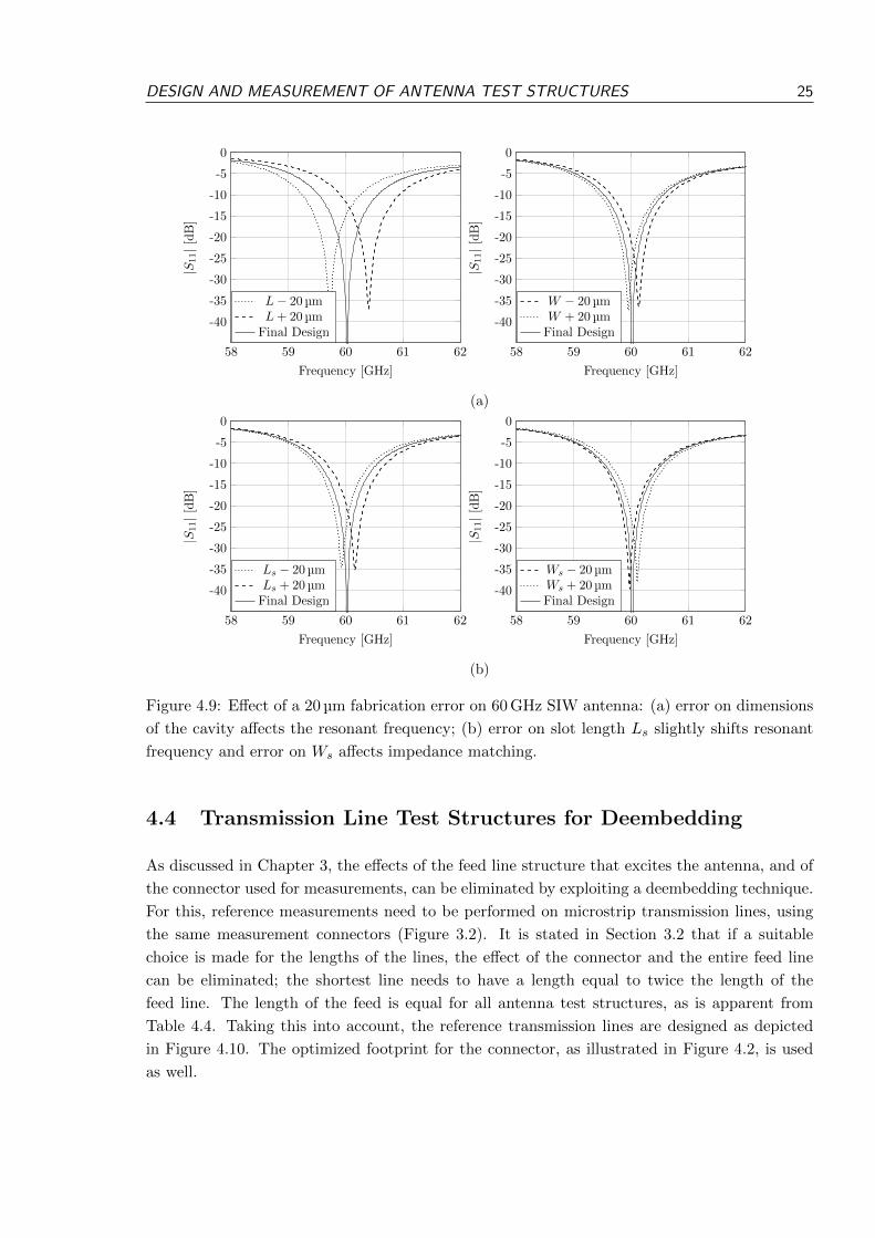
In a similar fashion as Section 4.2.2, the sensitivity of the parameters of the SIW antenna at
60 GHz are investigated. Once more, the worst case fabrication error is assumed to be 10% of
the minimum feature size allowed by the manufacturing process, i.e., 20 µm. An error on the
dimensions of the cavity, affects the resonant frequency, as depicted in Figure 4.9(a). An error
on the length of the slot Ls causes a slight shift in resonant frequency and an error on the
width Ws affects the impedance matching. This supports the theoretical analysis performed in
Section 2.3.2. It is clear from Figure 4.9 that the most critical parameters are the dimensions
of the cavity. An inaccuracy of 20 µm on the length of the cavity imposes a resonance shift of
approximately 300 MHz. To ensure that the cavity size is exact, the placement of the via wall
needs to be precise. If the row of vias is skewed, the dimensions of the cavity are altered and
the resonance is shifted. Moreover, if the spacing between the vias no longer complies with the
restrictions (2.14) due to inaccuracies, the equivalence with rectangular waveguides is lost and
the theoretical analysis of Section 2.3.2 no longer holds.
DESIGN AND MEASUREMENT OF ANTENNA TEST STRUCTURES 25
58 59 60 61 62
0
-5
-10
-15
-20
-25
-30
-35
-40
Frequency [GHz]
|S11|[
dB
]
L− 20 µmL+ 20 µm
Final Design
58 59 60 61 62
0
-5
-10
-15
-20
-25
-30
-35
-40
Frequency [GHz]
|S11|[
dB
]
W − 20 µmW + 20 µm
Final Design
(a)
58 59 60 61 62
0
-5
-10
-15
-20
-25
-30
-35
-40
Frequency [GHz]
|S11|[
dB
]
Ls − 20 µmLs + 20 µm
Final Design
58 59 60 61 62
0
-5
-10
-15
-20
-25
-30
-35
-40
Frequency [GHz]
|S11|[
dB
]
Ws − 20 µmWs + 20 µmFinal Design
(b)
Figure 4.9: Effect of a 20 µm fabrication error on 60 GHz SIW antenna: (a) error on dimensions
of the cavity affects the resonant frequency; (b) error on slot length Ls slightly shifts resonant
frequency and error on Ws affects impedance matching.
4.4 Transmission Line Test Structures for Deembedding
As discussed in Chapter 3, the effects of the feed line structure that excites the antenna, and of
the connector used for measurements, can be eliminated by exploiting a deembedding technique.
For this, reference measurements need to be performed on microstrip transmission lines, using
the same measurement connectors (Figure 3.2). It is stated in Section 3.2 that if a suitable
choice is made for the lengths of the lines, the effect of the connector and the entire feed line
can be eliminated; the shortest line needs to have a length equal to twice the length of the
feed line. The length of the feed is equal for all antenna test structures, as is apparent from
Table 4.4. Taking this into account, the reference transmission lines are designed as depicted
in Figure 4.10. The optimized footprint for the connector, as illustrated in Figure 4.2, is used
as well.

DESIGN AND MEASUREMENT OF ANTENNA TEST STRUCTURES 26
l2 = 51.5 mm
l1 = 2Lfeed = 21.5 mm
Figure 4.10: Designed reference transmission lines for deembedding of connector and feed line
structure.
4.5 Measurements
All S-parameter measurements presented in this section are performed with an N5247A Pro-
grammable Network Analyzer (PNA-X) from Keysight Technologies [21]. All reflection coeffi-
cients depicted below are the characteristics of the stand-alone antennas as discussed in Sec-
tion 3.3, i.e., deembedding of the connector and feed line is already performed. The deembedding
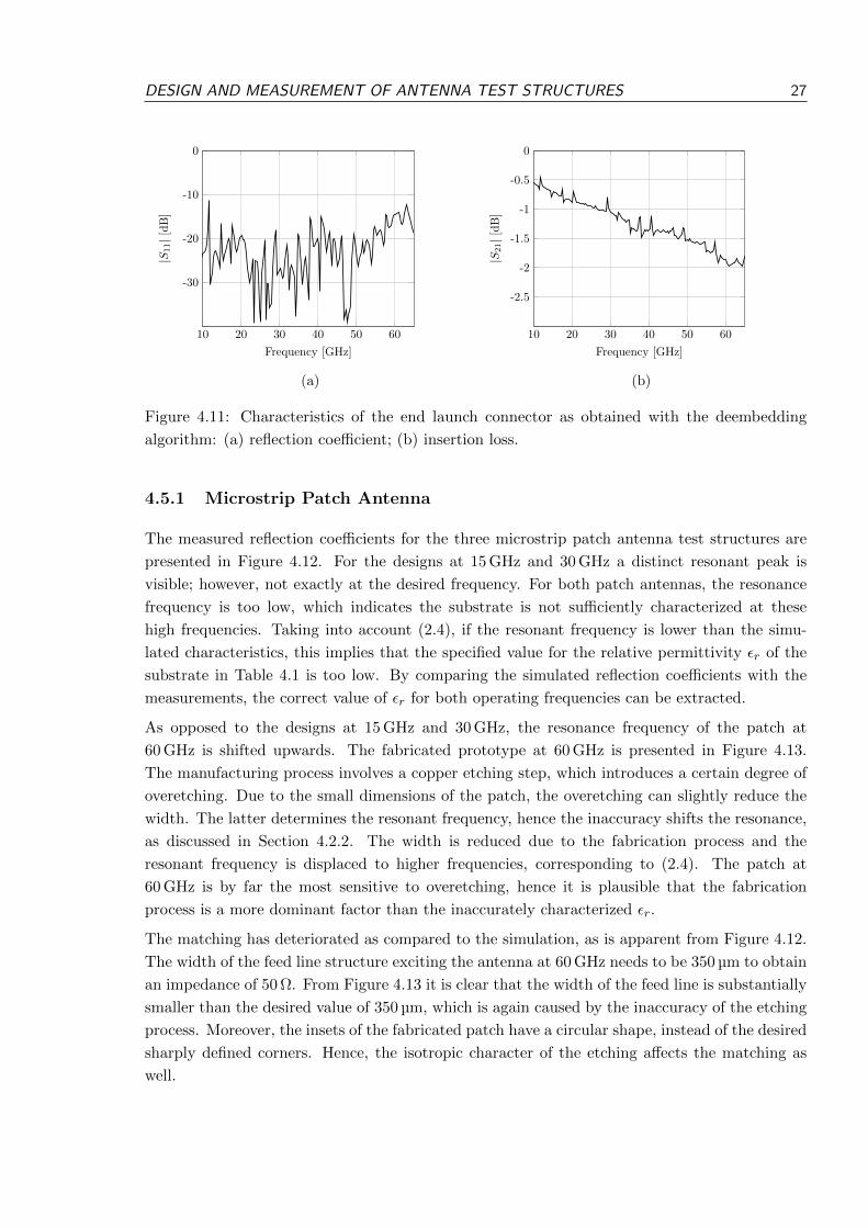
algorithm yields the characteristics of the end launch connector, as presented in Figure 4.11. It
is clear from Figure 4.11(b) that the connector introduces a maximum attenuation of 2 dB at
67 GHz. Looking at the overall trend of the reflection coefficient in Figure 4.11(a), it is perceived
that the matching deteriorates for rising frequencies. The fluctuations of the characteristics of
the connector are a result of the deembedding procedure. At each frequency where one of the
reference microstrip lines corresponds to a multiple of half a wavelength, a singularity occurs.
This also causes an additional ripple in the characteristics of the stand-alone antennas (see
further).
DESIGN AND MEASUREMENT OF ANTENNA TEST STRUCTURES 27
10 20 30 40 50 60
0
-10
-20
-30
Frequency [GHz]
|S11|[
dB
]
(a)
10 20 30 40 50 60
0
-0.5
-1
-1.5
-2
-2.5
Frequency [GHz]
|S21|[
dB
]
(b)
Figure 4.11: Characteristics of the end launch connector as obtained with the deembedding
algorithm: (a) reflection coefficient; (b) insertion loss.
4.5.1 Microstrip Patch Antenna
The measured reflection coefficients for the three microstrip patch antenna test structures are
presented in Figure 4.12. For the designs at 15 GHz and 30 GHz a distinct resonant peak is
visible; however, not exactly at the desired frequency. For both patch antennas, the resonance
frequency is too low, which indicates the substrate is not sufficiently characterized at these
high frequencies. Taking into account (2.4), if the resonant frequency is lower than the simu-
lated characteristics, this implies that the specified value for the relative permittivity εr of the
substrate in Table 4.1 is too low. By comparing the simulated reflection coefficients with the
measurements, the correct value of εr for both operating frequencies can be extracted.
As opposed to the designs at 15 GHz and 30 GHz, the resonance frequency of the patch at
60 GHz is shifted upwards. The fabricated prototype at 60 GHz is presented in Figure 4.13.
The manufacturing process involves a copper etching step, which introduces a certain degree of
overetching. Due to the small dimensions of the patch, the overetching can slightly reduce the
width. The latter determines the resonant frequency, hence the inaccuracy shifts the resonance,
as discussed in Section 4.2.2. The width is reduced due to the fabrication process and the
resonant frequency is displaced to higher frequencies, corresponding to (2.4). The patch at
60 GHz is by far the most sensitive to overetching, hence it is plausible that the fabrication
process is a more dominant factor than the inaccurately characterized εr.
The matching has deteriorated as compared to the simulation, as is apparent from Figure 4.12.
The width of the feed line structure exciting the antenna at 60 GHz needs to be 350 µm to obtain
an impedance of 50 Ω. From Figure 4.13 it is clear that the width of the feed line is substantially
smaller than the desired value of 350 µm, which is again caused by the inaccuracy of the etching
process. Moreover, the insets of the fabricated patch have a circular shape, instead of the desired
sharply defined corners. Hence, the isotropic character of the etching affects the matching as
well.

DESIGN AND MEASUREMENT OF ANTENNA TEST STRUCTURES 28
It is apparent from Figure 4.12(c) that the reflection coefficient remains rather low in the re-
gion between 58 GHz and 61 GHz. As discussed above, the matching of the patch to the feed
line structure is expected to be poor and the connector at the other end of the line introduces
mismatch as well. It is plausible that this evokes standing waves in the feed line; hence, the
microstrip is in resonance, which explains the low reflection coefficient. Moreover, the appar-
ent resonance at approximately 62 GHz can very well be caused by the same standing wave
phenomenon instead of a resonance of the patch.
14 14.5 15 15.5 16
0
-5
-10
-15
-20
Frequency [GHz]
|S11|[
dB
]
MeasuredSimulated
(a)
28 29 30 31 32
0
-5
-10
-15
-20
Frequency [GHz]
|S11|[
dB
]MeasuredSimulated
(b)
58 59 60 61 62 63 64
0
-5
-10
-15
-20
-25
-30
Frequency [GHz]
|S11|[
dB
]
MeasuredSimulated
(c)
Figure 4.12: Measured reflection coefficient for microstrip patch test structures: (a) at 15 GHz;
(b) at 30 GHz and (c) at 60 GHz.

DESIGN AND MEASUREMENT OF ANTENNA TEST STRUCTURES 29
300 µm
Overetching
Figure 4.13: Fabricated microstrip patch antenna at 60 GHz.
4.5.2 Cavity-Backed SIW Antenna
The measured reflection coefficients for the cavity-backed SIW antenna test structures are pre-
sented in Figure 4.14. The designs at 15 GHz and 30 GHz both exhibit a distinct resonance,
albeit at a frequency lower than the desired resonance. As already discussed in Section 4.5.1,
the shift of the resonance to lower frequencies is explained by the discrepancy in the relative
permittivity εr of the substrate material. Yet again, the antenna at 60 GHz exhibits the opposite
behavior; the resonance has shifted to a higher frequency. Figure 4.15 depicts the fabricated
SIW antenna at 60 GHz. As the frequency of the resonant TE120 mode (see Section 4.3) is
determined by the size of the cavity, the via placement needs to be very precise to achieve the
desired behavior. It is clear from Figure 4.15 that the via rows are skewed. This means the
cavity no longer has the desired dimensions, hence the resonance shifts.
As opposed to the microstrip patch antenna discussed in Section 4.5.1, the resonant frequency
is no longer subject to the effects of overetching, as it is determined by the cavity size. However,
overetching still affects the matching to the feed line structure; the dimensions of the insets need
to ensure a 50 Ω GCPW structure. It is clear that the isotropic nature of the etching process
influences the shape of the insets. From Figure 4.15 it can also be perceived that the microstrip
part of the feed line structure is too narrow to correspond with a 50 Ω impedance level. At
60 GHz the desired width of a 50 Ω microstrip line is 350 µm for this substrate material, while
the width of the fabricated specimen is approximately 290 µm. The matching of the fabricated
antenna has obviously worsened as compared to the simulations.

DESIGN AND MEASUREMENT OF ANTENNA TEST STRUCTURES 30
14 14.5 15 15.5 16
0
-5
-10
-15
-20
Frequency [GHz]
|S11|[
dB
]
MeasuredSimulated
(a)
29 29.5 30 30.5 31
0
-5
-10
-15
-20
-25
-30
Frequency [GHz]
|S11|[
dB
]
MeasuredSimulated
(b)
59 60 61 62 63 64
0
-5
-10
-15
-20
-25
Frequency [GHz]
|S11|[
dB
]
MeasuredSimulated
(c)
Figure 4.14: Measured reflection coefficient for cavity-backed SIW antenna test structures: (a)
at 15 GHz; (b) at 30 GHz and (c) at 60 GHz.
290 µm
Figure 4.15: Fabricated cavity-backed SIW antenna at 60 GHz.

DESIGN AND MEASUREMENT OF ANTENNA TEST STRUCTURES 31
4.6 Topology for Antenna Array
As discussed in Chapter 1, one of the main goals of this master’s dissertation is to develop a
highly compact and integratable antenna array. If the antenna system is to be integrated together
with other, likely active, electronic components, high isolation is a necessity. This ensures the
integrity of all signals and prevents crosstalk. As mentioned before, the SIW antenna provides
high isolation as a consequence of the metallized via wall forming the cavity. An additional
benefit of the high isolation is that the antenna elements in the array can be spaced closer
together without invoking high mutual coupling, as is clarified in Chapter 5.
A second goal is to ameliorate the bandwidth of the inherently bandlimited antennas. Different
techniques can be applied to enhance the bandwidth of both technologies. E.g., for the SIW
antenna, a technique based on hybrid modes can be exploited, whilst maintaining high isolation
and easy integration.
Even though losses are substantial at 60 GHz, the attenuation of the signal needs to be kept to a
minimum. It is proven through simulation and measurement that the SIW antenna has superior
performance over the patch when it comes to insertion loss. Considering the additional simu-
lation results obtained with MWS from CST, as discussed in Section 4.3.1, and the precedents
found in literature, the radiation efficiency of the SIW antenna is expected to be better as well.
Taking all of the above into account, the SIW technology is elected for the design of the 60 GHz
antenna array in the next chapter.

HYBRID MODE SIW ANTENNA ARRAY 32
Chapter 5
Hybrid Mode SIW Antenna Array
5.1 Hybrid Mode Cavity-Backed SIW Antenna
As proven in Chapter 4, cavity-backed SIW antennas are narrowband devices. The impedance
bandwidth depends on the matching condition, which is proportional to the antenna profile.
Due to the low-profile and high Q-factor of the resonant cavity, it is hard to achieve wideband
impedance matching when the cavity is only resonating at a single frequency. To overcome this
inherent disadvantage, a bandwidth enhancement technique based on hybrid modes is exploited.
5.1.1 Operating Mechanism
The bandwidth of a cavity-backed SIW antenna can be enhanced by simultaneously exciting two
hybrid modes inside the cavity and merging them within the desired frequency range as proposed
in [20]. The dominant fields of the hybrid modes are located in different half parts of the SIW
cavity, which are defined by the location of the slot. If the slot is off-center, the half parts will
have different dimensions and consequently support hybrid modes at different frequencies. By
tuning the size of both half cavities, the hybrid modes can be shifted in frequency and brought
close together. This will notably increase the impedance bandwidth of the antenna.
In essence, the hybrid modes are two different combinations of the TE110 and TE120 cavity
resonances. The hybrid mode with the lowest frequency, which is dominant in the largest
half cavity, is a combination of a strong TE110 and a weak TE120 resonance, as illustrated in
Figure 5.1(a). Accordingly, the hybrid mode with the highest frequency is dominant in the
smallest half cavity and consists of a strong TE120 and a weak TE110 resonance, as presented
in Figure 5.1(b). The field distribution of the higher hybrid mode (Figure 5.1(b)) displays a
large difference in phase and magnitude between the fields in both half cavities, hence effective
radiation can be generated from the slot. Although the fields are in phase for the lower hybrid
mode, radiation can still be generated due to the high difference in magnitude.

HYBRID MODE SIW ANTENNA ARRAY 33
(a)
(b)
Figure 5.1: Field distribution in the SIW cavity: (a) Dominant E-field distribution of lower
hybrid mode in largest half cavity; (b) Dominant E-field distribution of higher hybrid mode in
smallest half cavity [20].
5.1.2 Substrate Material
One of the main goals of this master’s dissertation is to develop a compact and highly integratable
antenna system. To push the integration aspect even further, a different substrate material than
for the antenna test structures is selected. For the design of the hybrid mode SIW array, a very
thin and flexible material is opted for. Concretely, DuPont™Pyralux® AP [22] flexible circuit
material is used. The design is made in duplicate; once on Pyralux AP9141 (50 µm substrate
thickness) and once on Pyralux AP8525 (100 µm substrate thickness). This way, the effects of
scaling down the substrate height can be assessed. The main characteristics of both materials
are summarized in Table 5.1.
AP9141 AP8525
εr 3.4 (1 MHz) 3.4 (1 MHz)
tan δ 0.002 (1 MHz) 0.002 (1 MHz)
thickness 100 µm 50 µm
Cu thickness 35 µm 18 µm
Table 5.1: Characteristics of Pyralux AP9141 and AP8525 flexible substrate material.
In [22], the dielectric constant and loss tangent are characterized up until 20 GHz. As the
array will operate at 60 GHz, additional characterization of the substrate material at this high
frequency is needed. To this end, a simple microstrip patch antenna at 60 GHz, with a well
defined resonant peak, will be fabricated on both substrates as well. By comparing the measured
characteristic of the patch with the simulations, the loss tangent and dielectric constant at

HYBRID MODE SIW ANTENNA ARRAY 34
60 GHz can be extracted.
One must take into account that the substrate materials used here are much thinner than the
ones used for the antenna test structures in Chapter 4. As discussed in Section 2.1, a thinner
substrate will decrease the maximum achieveable bandwidth.
5.1.3 Design
A general configuration for a hybrid mode cavity-backed SIW antenna is depicted in Figure 5.2.
The design procedure is very similar to that of a common cavity-backed SIW antenna. Firstly,
the dimensions of the cavity are obtained using (2.15), where the resonant frequency of the
TE110 mode needs to be 60 GHz. This yields an effective width Weff and length Leff, from which
the physical length Lc and width Wc of the cavity can be calculated using (2.11). Yet again, the
restrictions on the via spacing and diameter, as given in (2.14), need to be fulfilled to conserve
the equivalence with rectangular waveguides.
Once the cavity is designed, the slot can be added. A non-resonant slot is used, hence the slot
length Ls is larger than half a wavelength. In Chapter 4, the SIW antennas are designed with a
resonant slot, which implies that the resonant frequency can not only be affected by fabrication
errors on the cavity size, but on the slot as well. By designing the hybrid mode SIW antenna
with a slot length that is substantially larger than half a wavelength, an error on Ls will not
induce a shift of the resonance. The position of the slot determines the dimensions dc,u and dc,l
of the upper and lower half cavity, respectively. As stated before, the frequency of both hybrid
modes depends on the size of both half parts. If the slot is placed in the middle of the cavity, i.e.,
dc,u = dc,l, the hybrid modes coincide and a single resonance is perceived. The hybrid modes
can be pulled further apart by offsetting the slot from the center, i.e., by adjusting dc,u and dc,l.
For this design, it is assumed that dc,u > dc,l, hence the hybrid mode in the upper cavity is a
combination of a strong TE110 and a weak TE120. Equivalently, the mode in the lower cavity
consists of a strong TE120 and a weak TE110.
When dc,l increases, the area of the dominant resonant field of the higher hybrid mode increases,
which implies a decrease in resonant frequency. The area of the weak resonant field of the lower
hybrid mode is enlarged as well, but this only causes a slight decrease in resonant frequency. The
higher hybrid mode decreases in frequency, while the lower hybrid mode’s resonance remains
nearly unchanged, hence the net effect is a decrease of the impedance bandwidth. Alternatively,
when dc,u increases, the resonating area of the dominant field of the lower hybrid mode is
enlarged, hence its resonant frequency decreases. The resonating area of the weak field of the
higher frequency hybrid mode increases as well, but only causes a minor drop in frequency. In
this case, the lower hybrid mode decreases in frequency, while the higher hybrid mode remains
practicaly unchanged. This causes an enlargement of the impedance bandwidth.

HYBRID MODE SIW ANTENNA ARRAY 35
Ls Ws
dc,l
dc,u
Lc
Wc
Figure 5.2: General configuration of hybrid mode cavity-backed SIW antenna.
5.1.4 Simulation Results
The simulated reflection coefficients, depicted in Figure 5.3, clearly show two distinct resonant
peaks, i.e., two hybrid modes. The hybrid modes have resonant frequencies of 59.16 GHz and
60.38 GHz for the design on 50 µm substrate, and 59.18 GHz and 60.75 GHz for the design on
100 µm. The two modes are merged in the vicinity of 60 GHz, and as such, notably increase
the impedance bandwidth of the antennas. The fractional bandwidths are 3.6% and 4.5% for
the 50 µm and 100 µm design respectively. Taking into account that the bandwidth increases
monotonically with the substrate thickness [23], this implies an increase in impedance bandwidth
of 3% and 3.4%, respectively, as compared to the cavity-backed SIW antenna discussed in
Section 4.3.
58 59 60 61 62
0
-5
-10
-15
-20
-25
-30
-35
59.16 GHz 60.38 GHz
2.2 GHz
Frequency [GHz]
|S11|[
dB
]
(a)
58 59 60 61 62
0
-5
-10
-15
-20
-25
-30
-35
59.18 GHz 60.75 GHz
2.8 GHz
Frequency [GHz]
|S11|[
dB
]
(b)
Figure 5.3: Simulated reflection coefficient for hybrid mode SIW antenna: (a) substrate thickness
50 µm; (b) substrate thickness 100 µm.
Figure 5.4 depicts the simulated directivity and gain patterns in the E-plane for each hybrid

HYBRID MODE SIW ANTENNA ARRAY 36
mode of both designs. For both substrate thicknesses, the gain and directivity are lower for the
lower hybrid mode. The higher hybrid mode consists of a strong TE120 and weak TE110, and it
has been proven in [12] that elevated gains are achieved when a TE120 resonance is excited in
the cavity.
−15
−10
−5
0
5
10 dBi
90o
60o
30o
0o
−30o
−60o
−90o
(a)
−15
−10
−5
0
5
10 dBi
90o
60o
30o
0o
−30o
−60o
−90o
(b)
−15
−10
−5
0
5
10 dBi
90o
60o
30o
0o
−30o
−60o
−90o
(c)
−15
−10
−5
0
5
10 dBi
90o
60o
30o
0o
−30o
−60o
−90o
(d)
Figure 5.4: Simulated directivity (solid) and gain (dotted) in the E-plane: (a) at 59.16 GHz for
50 µm substrate; (b) at 60.38 GHz for 50 µm substrate; (c) at 59.18 GHz for 100 µm substrate;
(d) at 60.75 GHz for 100 µm substrate.
The E-field and H-field distributions inside the cavity for the 50 µm design are depicted in
Figure 5.5. From the E-field distribution at 59.16 GHz, presented in Figure 5.5(a), it is clear
that the field is dominant in the upper half cavity. As dc,u > dc,l was assumed in Section 5.1.3,
the upper cavity has the largest dimensions; this supports the fact that the lower hybrid mode
is dominant in the upper half cavity. From the H-field distribution for the lower hybrid mode in
Figure 5.5(b), one can ascertain that the fields in the half parts are in phase. Both the E-field
and the H-field distributions corroborate that the mode is indeed a combination of a strong
TE110 and a weak TE120, with a field distribution as already presented in Figure 5.1(a). An
analogous reasoning can be performed for the higher hybrid mode. The E-field distribution at
60.38 GHz in Figure 5.5(c) reveals that the higher hybrid mode is dominant in the smallest, lower
half cavity. The H-field in both half parts, depicted in Figure 5.5(d), is clearly in antiphase. Yet
again, both the electric and magnetic field confirm that the high frequency hybrid mode is a
combination of a strong TE120 and a weak TE110, which coincides with the theoretical analysis
of Section 5.1.1 and Figure 5.1(b).

HYBRID MODE SIW ANTENNA ARRAY 37
(a) (b)
(c) (d)
Figure 5.5: Simulated field distributions in the hybrid mode SIW cavity for 50 µm substrate: (a)
E-field at 59.16 GHz; (b) H-field at 59.16 GHz; (c) E-field at 60.38 GHz; (d) H-field at 60.38 GHz.
5.2 Uniform Linear Antenna Array
As demonstrated by the simulations performed in Chapter 4, the gain of a single antenna element
is limited and the radiation pattern is far from directive. High gain can be achieved by increasing
the electrical size of the antenna. By exploiting an array configuration, the gain can be increased
without enlarging the size of the individual elements. An array is, in essence, a collection of
radiating elements, placed in an electric and geometric configuration. Evidently, a new antenna
with a larger aperture size is formed.
The fields of the array elements will influence each other and the characteristics of an antenna
in an array configuration will deviate from the stand-alone characteristics. This is called mutual
coupling, but is often neglected. Vector addition of the fields of the seperate antenna elements
yields the total field of the array. Depending on the direction, the fields will interfere con-
structively or destructively. By electronically controlling the way the distinct elements are fed,
constructive interference can be obtained in any desired direction; this yields a highly directive
radiation pattern.
There is an abundance of possible array configurations. Here, the Uniform Linear Array (ULA)
configuration is adopted. It consists of N identical antenna elements placed along a line with
constant spacing a. If the total far-field radiation vector of a single antenna element is defined as

HYBRID MODE SIW ANTENNA ARRAY 38
F (θ, φ) and mutual coupling is indeed neglected, the radiation pattern of the array only differs
from that of a single element by the array factor T (θ, φ). The latter is only valid in the far-field,
i.e., the fields are observed at distances much larger than the dimension of the aperture. The
array factor for a ULA with evenly spaced antenna elements along the y-axis is defined as [24]
T (θ, φ) =N−1∑n=0
Anejβnejnk0a sinφ sin θ, (5.1)
where An and βn are, respectively, the amplitude and phase by which the nth element is excited,
θ the elevation angle and φ the azimuth angle. All array elements will be excited with equal
phase βn = 0 and magnitude An = A, as to construct a broadside array. Moreover, if one limits
the analysis to the azimuth plane (θ = π2 ), the array factor becomes [24]
T (φ) = A
N−1∑n=0
ejnk0a sinφ
= NAejN−1
2(k0a sinφ) sin
(N2 k0a sinφ
)N sin
(12k0a sinφ
) . (5.2)
Focussing on the amplitude of the array factor, the direction of maximum radiation φ0 is given
by
k0a sinφ = 0
=⇒ φ0 = 0°, −π2≤ φ ≤ π
2, (5.3)
which confirms that the array indeed radiates in the broadside direction. The orientation of the
maximum radiation is independent of the antenna element spacing a. Equivalently, the nulls of
the radiation pattern are given by
φ = arcsin
[± λ
2πa
2m
Nπ
], −π
2≤ φ ≤ π
2, (5.4)
with N being the number of antenna elements in the array and m = 1, 2, 3, .... The argument
of the arcsine cannot exceed unity, hence there is a limited number of zeroes. The amount of
zeroes is a function of the element spacing a and the number of antennas in the array N . If a
or N increases, the number of nulls in the radiation pattern will increase as well and the width
of the main beam will evidently decrease.
5.3 Array Design
Four hybrid mode cavity-backed SIW antennas, as developed in Section 5.1, are now exploited
to construct a broadside ULA. The array configuration yields elevated gain and the enlarged
aperture provides a narrower mainbeam, i.e., the directivity is raised as well. The elements are

HYBRID MODE SIW ANTENNA ARRAY 39
spaced by a distance a and the ports are numbered in ascending order from left to right, as
depicted in Figure 5.6. All elements are excited with identical phase and amplitude to point the
main beam in the broadside direction.
a aa
1 2 3 4
Figure 5.6: Hybrid mode SIW antennas in a four-element broadside ULA with spacing a.
5.3.1 Mutual Coupling Between Array Elements
As discussed in Section 5.2, an antenna array is designed under the assumption that mutual cou-
pling between the seperate elements can be neglected. For this to be true, the array elements
need to be spaced by a certain distance, hence maintaining low coupling. The spacing of the ele-
ments affects the width of the main beam, i.e., the directivity, as proven in Section 5.2. The core
of the antenna elements is the SIW cavity, which provides high isolation of the fields. Because
of this, it is of practical interest to investigate the minimal spacing of the elements for which
the mutual coupling is still low enough to be neglected. It is most likely that, due to the high
isolation, the elements can be spaced more closely, which is beneficial for the integration aspect
of the antenna system. Figure 5.8 depicts the mutual coupling between the array elements for
various spacings a, for the design on 50 µm substrate. Obviously, the mutual coupling increases
as the element spacing a decreases. Comparing Figure 5.8(a) with Figure 5.8(b), an increase
of approximately 4 dB is visible in the S21 characteristic when a decreases from λ2 to λ
4 . The
S21 signifies the mutual coupling between adjacent elements in the array; as the configuration
is symmetrical, this also equals S32 and S43. Even with a spacing of a quarter wavelength the
mutual coupling remains below −25 dB. It stands to reason that the elements can be brought
even closer together. To exploit the integration aspect to the utmost extent, the mutual coupling
is investigated for the case where the via row is reused for adjacent array elements, as illustrated
in Figure 5.7. The simulated mutual coupling is presented in Figure 5.8(c). The mutual coupling
for the design on the 100 µm substrate is equivalent and an analogous reasoning is performed.
Figure 5.7: Via wall is reused for adjacent array elements.

HYBRID MODE SIW ANTENNA ARRAY 40
58 59 60 61 62
-10
-20
-30
-40
-50
Frequency [GHz]
Mutu
alco
upling
[dB
]
|S21||S31||S41|
(a)
58 59 60 61 62
-10
-20
-30
-40
-50
Frequency [GHz]
Mutu
alco
upling
[dB
]
|S21||S31||S41|
(b)
58 59 60 61 62
-10
-20
-30
-40
-50
Frequency [GHz]
Mutu
alco
upling
[dB
]
|S21||S31||S41|
(c)
Figure 5.8: Simulated mutual coupling between array elements for 50 µm substrate: (a) element
spacing a = λ2 ; (b) element spacing a = λ
4 ; (c) reusing via wall for adjacent elements.
5.3.2 Simulation Results
It is clear from Figure 5.8(c) that the mutual coupling remains below −20 dB, even if the via
wall is reused for adjoining antennas. This particular configuration is only feasible if the amount
of coupling does not profoundly change the frequency characteristic of the array as compared
to the characteristic of the seperate elements. This comparison is depicted in Figure 5.9. It is
clear that for both designs the elevated mutual coupling, induced by reusing the via wall, does
not detrementally impact the frequency characteristic of the array. Moreover, this configuration
yields a more compact and integrateable antenna system.
Figure 5.10 depicts the simulated directivity and gain of the array configuration. The direction
of the main beam is indeed broadside (φ = 0). The nulls in the radiation pattern due to the array
configuration are clearly visible as well; a more directive, narrower beam is achieved as compared
to the stand-alone hybrid mode SIW antenna (Figure 5.4). Furthermore, a notable increase
in gain and directivity can be perceived. For the 50 µm substrate, the gain and directivity
in the broadside direction are respectively 4.6 dBi and 8.6 dBi for the lower hybrid mode at

HYBRID MODE SIW ANTENNA ARRAY 41
59.16 GHz, and 7.2 dBi and 12.0 dBi for the hybrid mode at 60.38 GHz. The higher hybrid
mode achieves more gain due to the strong TE120 resonance, in the array configuration as
well. The array designed for the 100 µm substrate exhibits similar performance, as illustrated
in Figures 5.10(c) and 5.10(d).
58 59 60 61 62
0
-10
-20
-30
Frequency [GHz]
|S11|[
dB
]
Reuse via wallSeperate element
(a)
58 59 60 61 62
0
-10
-20
-30
Frequency [GHz]
|S11|[
dB
]
Reuse via wallSeperate element
(b)
Figure 5.9: Simulated reflection coefficients for the hybrid mode SIW broadside ULA as com-
pared to the reflection coefficient of a seperate element: (a) 50 µm substrate (b) 100 µm substrate.
−10
−5
0
5
10
15 dBi
90o
60o
30o
0o
−30o
−60o
−90o
(a)
−10
−5
0
5
10
15 dBi
90o
60o
30o
0o
−30o
−60o
−90o
(b)
−10
−5
0
5
10
15 dBi
90o
60o
30o
0o
−30o
−60o
−90o
(c)
−10
−5
0
5
10
15 dBi
90o
60o
30o
0o
−30o
−60o
−90o
(d)
Figure 5.10: Simulated directivity (solid) and gain (dotted) in the E-plane of the hybrid mode
SIW array: (a) at 59.16 GHz for 50 µm substrate; (b) at 60.38 GHz for 50 µm substrate; (c) at
59.18 GHz for 100 µm substrate; (d) at 60.75 GHz for 100 µm substrate.

HYBRID MODE SIW ANTENNA ARRAY 42
5.3.3 Wilkinson Power Divider for Feed Network
To arrive at a broadside ULA, all four antenna elements need to be fed with equal amplitude
and phase. This implies that the incoming power will need to be equally four-way divided. To
achieve this, the Wilkinson Power Divider (WPD) is exploited in a corporate feed configuration.
Corporate feeding is essentialy parallel feeding, i.e., all excitations have the same amplitude and
phase. Three WPDs are used in the configuration as depicted in Figure 5.11. As the power is
divided into two equal parts by every WPD, each divider stage introduces an additional 3 dB
signal loss.
50 ΩVs
Port plane
WPD
WPD
WPD
Figure 5.11: WPDs in corporate feed network for ULA.
The WPD makes use of a quarter-wave transformer to attain impedance matching at its input
port. Figure 5.12 depicts a Wilkinson Power Divider in microstrip technology. The input port
is matched to the two output ports using a quarter wavelength transmission line section with an
impedance of√
2Z0. Isolation between the two output ports is procured by the added lumped
resistor with impedance 2Z0. If power reflects at port 2, it will be absorbed by the resistor
instead of coupling to port 3 and vice versa.
The designed corporate feed network for the 50 µm substrate is depicted in Figure 5.14. The
characteristics are presented in Figure 5.13. The reflection coefficient in the desired frequency
range at the input port (Figure 5.13(a)) is below −40 dB and at the output ports (Figure 5.13(b))
it remains below −25 dB. Hence, excellent matching is achieved. The coupling between two
adjacent output ports (Figure 5.13(c)) is below −20 dB due to the added lumped resistor. The
additional signal loss from input to output induced by the two stage divider is of the order of
6 dB as expected (Figure 5.13(d)).
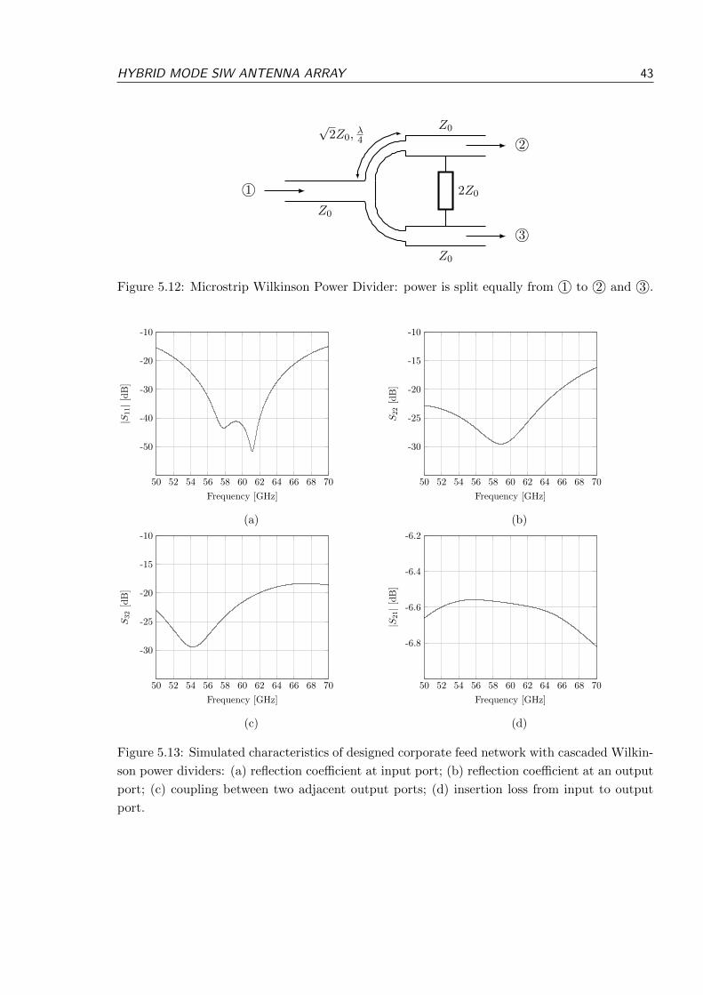
HYBRID MODE SIW ANTENNA ARRAY 43
√2Z0,
λ4
1
2
3
Z0
Z0
Z0
2Z0
Figure 5.12: Microstrip Wilkinson Power Divider: power is split equally from 1 to 2 and 3.
50 52 54 56 58 60 62 64 66 68 70
-10
-20
-30
-40
-50
Frequency [GHz]
|S11|[
dB
]
(a)
50 52 54 56 58 60 62 64 66 68 70
-10
-15
-20
-25
-30
Frequency [GHz]
S22
[dB
]
(b)
50 52 54 56 58 60 62 64 66 68 70
-10
-15
-20
-25
-30
Frequency [GHz]
S32
[dB
]
(c)
50 52 54 56 58 60 62 64 66 68 70
-6.2
-6.4
-6.6
-6.8
Frequency [GHz]
|S21|[
dB
]
(d)
Figure 5.13: Simulated characteristics of designed corporate feed network with cascaded Wilkin-
son power dividers: (a) reflection coefficient at input port; (b) reflection coefficient at an output
port; (c) coupling between two adjacent output ports; (d) insertion loss from input to output
port.

HYBRID MODE SIW ANTENNA ARRAY 44
5.3.4 Influence of Feed Network
The designed hybrid mode SIW array with added corporate feed network is depicted in Fig-
ure 5.14. The feed network obviously introduces additional losses, as proven by simulation in
Section 5.3.3 and presented in Figure 5.15. As the signal first needs to travel through the corpo-
rate feed network, a substantial amount of extra attenuation occurs due to copper, substrate and
radiation losses before it reaches the actual antenna. Moreover, the feed network will introduce
additional radiation, which will interfere with the desired radiation coming from the array.
Figure 5.14: Designed hybrid mode SIW array with added corporate feed network.
58 59 60 61 62
0
-5
-10
-15
-20
-25
-30
-35
Frequency [GHz]
|S11|[
dB
]
Figure 5.15: Simulated reflection coefficient for the hybrid mode SIW array with added corporate
feed network.

HYBRID MODE SIW ANTENNA ARRAY 45
5.4 Measurements
The fabricated hybrid mode SIW antenna array on 100 µm flexible substrate is depicted in
Figure 5.16. Measurements indicate that the degree of overetching is notably lower than for the
designs in Section 4.5. The width of the 50 Ω microstrip traces is approximately equal to the
desired 210 µm. The holes for the conductive vias are created with a laser ablation process. For
the limited diameter of 200 µm this yields the highest possible accuracy. Compared to the drilled
via rows of the SIW antenna in Figure 4.15, it is clear that the placement with laser ablation is
notably more accurate. As Uniform Thickness Copper Plating (UTCP) processing of the vias
is not feasible for such a small quantity of prototypes, grounding of the top layer is provided by
injecting electrically conductive paste into the holes and pressing it down with a stencil. The
performance of this conducting paste is not well known at frequencies as high as 60 GHz, hence
some undesired effects are highly plausible to occur.
3 mm
Figure 5.16: Fabricated hybrid mode SIW antenna on 100 µm substrate.
The fabricated antenna array is presented in more detail in Figure 5.17. As explained above, the
conductive paste is pushed into the holes to ensure a good connection. Doing so, some spillage of
the paste ends up in the slot and the insets. After fabrication, the insets are completely sealed,
i.e., reducing the inset depth to zero, which is detrimental for the impedance matching. The
slots are partially occupied by the conductive material as well, plausibly affecting the proper
operation of the antenna array. As explained in Section 2.3.2, the slot is an important tuning
element for the impedance matching. Attempts have been made to clear both the insets and
the slot of the paste spillage. Still, some residue remains, as depicted in Figure 5.17.

HYBRID MODE SIW ANTENNA ARRAY 46
paste in inset
paste in slot
850 µm
Figure 5.17: Detail of fabricated hybrid mode SIW antenna array.
Measurements are performed using the SouthWest Microwave end launch connectors, discussed
in Section 4.1, and an N5247A PNA-X from Keysight Technologies [21]. These revealed that
standing waves occur in the corporate feed network of the array, as depicted in Figure 5.18. A
resonance occurs, approximately, every 5 GHz, which corresponds to a wavelength of circa 3.2 cm
inside the substrate material. The combined length of the microstrip feed line and the corporate
feed network corresponds to approximately half a wavelength at 5 GHz. This implies that a
resonance occurs whenever the length of the feed structure is a multiple of half a wavelength. A
standing wave is formed when two waves of the same frequency propagate in opposite directions,
i.e., when reflections occur at both ends of the feed network. Hence, the impedance of the SIW
antenna has changed significantly and is no longer properly matched to the 50 Ω feed line. This
can be attributed to the discrepancy in the size of the insets and the slot. Another hypothesis is
that the impedance of the SIW antenna has drastically changed due to the non-ideal electrical
properties of the paste at these high frequencies. The standing wave signifies that the impedance
matching at the connector end of the line is not sufficient either. As the dimensions of the 50 Ωmicrostrip are accurate, this indicates that there is an amount of mismatch at the junction
between the connector and the circuit. The thickness of the flexible substrate is substantially
less than in Chapter 4. Although proper operation for any board thickness is assured in [17], it
stands to reason that the press fit of the connector no longer ensures a good connection. Also,
the characteristics of the substrate are not precisely known at 60 GHz; if these have gravely
changed as compared to the values in Table 5.1, that could explain the faulty matching as well.

HYBRID MODE SIW ANTENNA ARRAY 47
40 45 50 55 60 65
0
-5
-10
-15
-20
-25
-30
-35
Frequency [GHz]
|S11|[
dB
]
Figure 5.18: Measured reflection coefficient for the fabricated hybrid mode SIW array on 50 µm
substrate.
To gain insight into the effects at hand, one of the reference microstrip lines for deembedding the
connector and feed line structure is measured. The characteristics are depicted in Figure 5.19.
The reflection coefficient in Figure 5.19(a) demonstrates that the matching of the line to the con-
nector is poor, i.e., above −10 dB on average. From the measured insertion loss in Figure 5.19(b)
it is clear that a considerable amount of attenuation is introduced. As stated above, the width of
the trace is accurate, hence the faulty matching is not caused by a fabrication inaccuracy. This
implies that the additional losses and inferior matching are due to the combination of unknown
substrate and connector characteristics.
To quantify the amount of additional losses that is introduced, the power balance of the line is
calculated. For an ideal, lossless transmission line it holds that [25]
|S11|2 + |S21|2 = 1, (5.5)
which denotes that all incident power at port 1 is either reflected back to the source or trans-
mitted to port 2. For a lossy transmission line this power balance becomes
|S11|2 + |S21|2 + Ploss + Prad = 1, (5.6)
where Ploss is the normalized power that is dissipated due to substrate and copper losses, and
Prad is the normalized power radiated into free space. Figure 5.20 depicts the power balance for
the measured reference microstrip line. It is clear that a substantial amount of power is lost,
70% on average. This indicates that the substrate material is notably more lossy than suggested
by the characteristics in Table 5.1, hence it is insufficiently characterized at 60 GHz.

HYBRID MODE SIW ANTENNA ARRAY 48
50 52 54 56 58 60 62 64 66 68
0
-10
-20
-30
-40
Frequency [GHz]
|S11|[
dB
]
(a)
50 52 54 56 58 60 62 64 66 68
-5
-6
-7
-8
-9
Frequency [GHz]
|S21|[
dB
]
(b)
Figure 5.19: Measured characteristics of the reference microstrip line for deembedding: (a)
reflection coefficient; (b) insertion loss.
50 52 54 56 58 60 62 64 66 680
0.2
0.4
0.6
0.8
1
Frequency [GHz]
|S11|2
+|S
21|2
Figure 5.20: Power balance for the measured reference microstrip line.
CONCLUSION AND FUTURE RESEARCH 49
Chapter 6
Conclusion and Future Research
The goal of this master’s dissertation was to design a highly compact and integratable antenna
array that operates in the 60 GHz band, whilst maintaining compatibility with standard printed
circuit board processing steps. Firstly, antenna test structures, in both microstrip patch and
Substrate Integrated Waveguide (SIW) technology, at different frequencies were developed to
make an assessment of the impact of high frequency effects. This brought forth a comparative
study of both technologies, based on both simulation and measurement results, and enabled the
formulation of a founded opinion that SIW is the most advantageous technology for the design
of the array.
The analysis of the SIW antenna test structures has confirmed the inherent band limited be-
havior of this technology, which is due to the high Q-factor of the resonance and the low profile.
A bandwidth enhancement technique based on hybrid mode excitation was proposed and suc-
cessfully executed. Simulated fractional impedance bandwidths of 3.6% and 4.5% were achieved
at 60 GHz on extremely thin substrates. To push the integration aspect of the dissertation to
the utmost extent, it was opted to design and fabricate the hybrid mode SIW antenna array
on 50 µm and 100 µm flexible substrate material. Moreover, exploiting a Uniform Linear Array
(ULA) configuration with four antenna elements, high gain and directivity were achieved, i.e.,
7.2 dBi and 12.0 dBi, respectively.
The insufficient characterization of the flexible substrate at 60 GHz and the non-ideal processing
of the minute vias were detrimental for the operation of the fabricated prototypes. Future
research on this topic could certainly encompass investigating the characteristics of flexible
substrates for antenna design at 60 GHz, or even research towards the development of novel
flexible substrate materials for use in the Extremely High Frequency (EHF) band.
The fabricaton process aside, future development can certainly cover a beam forming system,
which could be utilized in, for example, systems that provide a Wireless Local Access Network
(WLAN) in the 60 GHz band in office environments. Due to the beam forming, spacial selectivity
is achieved; this enables multiple systems to work side-by-side without causing interference.
Higher bandwidths, and correspondingly higher bit rates, can be offered to the mobile user.
Further research could be performed towards phase shifter circuits operating at 60 GHz as well.

CONCLUSION AND FUTURE RESEARCH 50
Combined with the hybrid mode SIW array and a Digital Signal Processing (DSP) unit, an
adaptive beam steering system could be developed. Adjusting the respective phases of the
excitations of the antennas in the array allows for scanning. This means the direction of maxi-
mum radiation is moved electronically, which could find its application in millimeter wave radar
detection systems.
If the bandwidth of the hybrid mode SIW antenna can be enlarged even further or research is
performed towards Ultra Wideband (UWB) SIW antennas, radar operation based on very short
pulses is possible. Applications could be, for example, an indoor positioning system. Due to
the UWB operation of the antenna, the round trip time of a very short pulse can be measured,
which allows triangulation.

BIBLIOGRAPHY 51
Bibliography
[1] Federal Communications Commision. (2013) Part 15 Rules for Unlicensed
Operation in the 57-64 GHz Band [Online]. http://www.fcc.gov/document/
part-15-rules-unlicensed-operation-57-64-ghz-band.
[2] F. D. Paolo, Networks and Devices Using Planar Transmission Lines. CRC Press LLC,
2000.
[3] D. M. Pozar, Microwave Engineering. John Wiley and Sons Inc., 2012.
[4] N. G. Alexopoulos and D. R. Jackson, “Fundamental Superstrate (Cover) Effects on Printed
Circuit Antennas,” IEEE Transactions on Antennas and Propagation, vol. AP-32, no. 8,
Aug 1984.
[5] C. A. Balanis, Antenna Theory: Analysis and Design. John Wiley and Sons Inc., 2005.
[6] ——, Advanced Engineering Electromagnetics. John Wiley and Sons Inc., 1989.
[7] E. O. Hammerstad, “Equations for Microstrip Circuit Design,” in Proc. Fifth European
Microwave Conf., 1975.
[8] C. A. Balanis, Modern Antenna Handbook. John Wiley and Sons Inc., 2012.
[9] Y. Cassivi, L. Perregrini, P. Arcioni, M. Bressan, K. Wu, and G. Conciauro, “Disper-
sion Characteristics of Substrate Integrated Rectangular Waveguide,” IEEE Microwave
and Wireless Components Letters, vol. 12, no. 9, 2002.
[10] F. Xu and K. Wu, “Guided-Wave and Leakage Characteristics of Substrate Integrated
Waveguide,” IEEE Transactions on Microwave Theory and Techniques, vol. 53, no. 1, 2005.
[11] H. Kang and S. Lim, “Enhanced-Gain Planar Substrate-Integrated Waveguide Cavity-
Backed Slot Antenna with Rectangular Slot Window on Superstrate,” ETRI Journal, 2014.
[12] G. Q. Luo, Z. F. Hu, L. X. Dong, and L. L. Sun, “Planar Slot Antenna Backed by Substrate
Integrated Waveguide Cavity,” IEEE Antennas and Wireless Propagation Letters, vol. 7,
2008.
[13] R. Mavaddat, Network Scattering Parameters. World Scientific Publishing Co. Pte. Ltd.,
1996.

BIBLIOGRAPHY 52
[14] G. P. Srivastava and V. L. Gupta, Microwave Devices and Circuit Design. Prentice-Hall
of India Pvt.Ltd, 2006.
[15] F. Declercq, H. Rogier, and C. Herteleer, “Permittivity and Loss Tangent Characterization
for Garment Antennas Based on a New Matrix-Pencil Two-Line Method,” IEEE Transac-
tions on Antennas and Propagation, vol. 56, no. 8, 2008.
[16] Rogers Corporation. RO4000® Series High Frequency Circuit Materials, Techni-
cal Datasheet [Online]. Available: http://www.rogerscorp.com/documents/726/acs/
RO4000-LaminatesData-sheet.pdf.
[17] Southwest Microwave. (2007) Southwest Microwave End Launch Connector [Online]. http:
//mpd.southwestmicrowave.com/products/endLaunch.php.
[18] ——. (2007) Optimizing Test Boards for 50 GHz End Launch Connectors, Datasheet [On-
line]. http://mpd.southwestmicrowave.com/showImage.php?image=439.
[19] R. S. Elliott, Antenna Theory and Design. John Wiley and Sons Inc., 2003.
[20] G. Q. Luo, Z. F. Hu, W. J. Li, X. H. Zhang, L. L. Sun, and J. F. Zheng, “Bandwidth-
Enhanced Low-Profile Cavity-Backed Slot Antenna by Using Hybrid SIW Cavity Modes,”
IEEE Transactions on Antennas and Propagation, vol. 60, no. 4, 2012.
[21] Keysight Technologies. Keysight 2-Port and 4-Port PNA-X Network Analyzer N5247A - 10
MHz to 67 GHz, Technical Datasheet [Online]. Available: http://literature.cdn.keysight.
com/litweb/pdf/N5247-90002.pdf?id=1994005.
[22] DuPont™. DuPont™Pyralux® AP flexible circuit materials, Technical Datasheet
[Online]. Available: http://www.dupont.com/content/dam/assets/products-and-services/
electronic-electrical-materials/assets/PyraluxAPclad DataSheet.pdf.
[23] D. M. Pozar and D. H. Schaubert, Microstrip Antennas: The Analysis and Design of
Microstrip Antennas and Arrays. John Wiley and Sons Inc., 1995.
[24] H. Rogier, “Antennas and Propagation,” Ghent University 2013-2014, unpublished syllabus.
[25] H. Rogier and D. Vande Ginste, “Circuit and EMC Concepts,” Ghent University 2013-2014,
unpublished syllabus.

LIST OF FIGURES 53
List of Figures
2.1 Simple microstrip patch antenna configuration. . . . . . . . . . . . . . . . . . . . 4
2.2 Fringing E-fields as radiation mechanism for a patch antenna. . . . . . . . . . . . 5
2.3 Microstrip patch antenna with insets for impedance matching. . . . . . . . . . . . 7
2.4 SIW structure: conductive vias connecting parallel copper planes. . . . . . . . . . 7
2.5 SIW resonant cavity with microstrip line feed. . . . . . . . . . . . . . . . . . . . . 9
3.1 Cascade of two arbitrary two-port networks. . . . . . . . . . . . . . . . . . . . . . 11
3.2 Microstrip lines with coax-to-microstrip transitions SA and SB and ideal lossy
transmission line section SL. . . . . . . . . . . . . . . . . . . . . . . . . . . . . . 12
3.3 Piece of 50 Ω transmission line with connector modeled as 35 Ω discontinuity. . . 13
3.4 S-parameter simulation performed on modeled connector. . . . . . . . . . . . . . 13
3.5 Characteristic of model connector: extracted with deembedding algorithm (solid
line) and simulated with circuit solver (dashed line). . . . . . . . . . . . . . . . . 14
3.6 Block diagram of measurement to be performed. . . . . . . . . . . . . . . . . . . 14
4.1 Southwest Microwave 1.85 mm end launch connector. . . . . . . . . . . . . . . . . 17
4.2 Connector footprint with GCPW launch structure. . . . . . . . . . . . . . . . . . 17
4.3 Simulated reflection coefficient for patch antenna test structures: (a) at 15 GHz;
(b) at 30 GHz and (c) at 60 GHz. . . . . . . . . . . . . . . . . . . . . . . . . . . . 19
4.4 Simulated directivity (solid) and gain (dotted) in the E-plane of the antenna: (a)
at 15 GHz, (b) at 30 GHz and (c) at 60 GHz. . . . . . . . . . . . . . . . . . . . . . 20
4.5 Effect of a 20 µm fabrication error on the 60 GHz patch: (a) error on W affects
the resonant frequency; (b) error on R affects the matching. . . . . . . . . . . . . 20
4.6 Simulated reflection coefficient for cavity-backed SIW antenna test structures: (a)
at 15 GHz; (b) at 30 GHz and (c) at 60 GHz. . . . . . . . . . . . . . . . . . . . . . 22
4.7 E-field inside the cavity of the SIW antenna at 60 GHz: TE120 resonance. . . . . 23
4.8 Simulated directivity (solid) and gain (dotted) in the E-plane of the SIW antenna:
(a) at 15 GHz; (b) at 30 GHz and (c) at 60 GHz. . . . . . . . . . . . . . . . . . . 24
LIST OF FIGURES 54
4.9 Effect of a 20 µm fabrication error on 60 GHz SIW antenna: (a) error on dimen-
sions of the cavity affects the resonant frequency; (b) error on slot length Ls
slightly shifts resonant frequency and error on Ws affects impedance matching. . 25
4.10 Designed reference transmission lines for deembedding of connector and feed line
structure. . . . . . . . . . . . . . . . . . . . . . . . . . . . . . . . . . . . . . . . . 26
4.11 Characteristics of the end launch connector as obtained with the deembedding
algorithm: (a) reflection coefficient; (b) insertion loss. . . . . . . . . . . . . . . . 27
4.12 Measured reflection coefficient for microstrip patch test structures: (a) at 15 GHz;
(b) at 30 GHz and (c) at 60 GHz. . . . . . . . . . . . . . . . . . . . . . . . . . . . 28
4.13 Fabricated microstrip patch antenna at 60 GHz. . . . . . . . . . . . . . . . . . . . 29
4.14 Measured reflection coefficient for cavity-backed SIW antenna test structures: (a)
at 15 GHz; (b) at 30 GHz and (c) at 60 GHz. . . . . . . . . . . . . . . . . . . . . . 30
4.15 Fabricated cavity-backed SIW antenna at 60 GHz. . . . . . . . . . . . . . . . . . 30
5.1 Field distribution in the SIW cavity: (a) Dominant E-field distribution of lower
hybrid mode in largest half cavity; (b) Dominant E-field distribution of higher
hybrid mode in smallest half cavity [20]. . . . . . . . . . . . . . . . . . . . . . . . 33
5.2 General configuration of hybrid mode cavity-backed SIW antenna. . . . . . . . . 35
5.3 Simulated reflection coefficient for hybrid mode SIW antenna: (a) substrate thick-
ness 50 µm; (b) substrate thickness 100 µm. . . . . . . . . . . . . . . . . . . . . . 35
5.4 Simulated directivity (solid) and gain (dotted) in the E-plane: (a) at 59.16 GHz
for 50 µm substrate; (b) at 60.38 GHz for 50 µm substrate; (c) at 59.18 GHz for
100 µm substrate; (d) at 60.75 GHz for 100 µm substrate. . . . . . . . . . . . . . . 36
5.5 Simulated field distributions in the hybrid mode SIW cavity for 50 µm substrate:
(a) E-field at 59.16 GHz; (b) H-field at 59.16 GHz; (c) E-field at 60.38 GHz; (d)
H-field at 60.38 GHz. . . . . . . . . . . . . . . . . . . . . . . . . . . . . . . . . . . 37
5.6 Hybrid mode SIW antennas in a four-element broadside ULA with spacing a. . . 39
5.7 Via wall is reused for adjacent array elements. . . . . . . . . . . . . . . . . . . . . 39
5.8 Simulated mutual coupling between array elements for 50 µm substrate: (a) ele-
ment spacing a = λ2 ; (b) element spacing a = λ
4 ; (c) reusing via wall for adjacent
elements. . . . . . . . . . . . . . . . . . . . . . . . . . . . . . . . . . . . . . . . . 40
5.9 Simulated reflection coefficients for the hybrid mode SIW broadside ULA as com-
pared to the reflection coefficient of a seperate element: (a) 50 µm substrate (b)
100 µm substrate. . . . . . . . . . . . . . . . . . . . . . . . . . . . . . . . . . . . 41
5.10 Simulated directivity (solid) and gain (dotted) in the E-plane of the hybrid mode
SIW array: (a) at 59.16 GHz for 50 µm substrate; (b) at 60.38 GHz for 50 µm
substrate; (c) at 59.18 GHz for 100 µm substrate; (d) at 60.75 GHz for 100 µm
substrate. . . . . . . . . . . . . . . . . . . . . . . . . . . . . . . . . . . . . . . . . 41
LIST OF FIGURES 55
5.11 WPDs in corporate feed network for ULA. . . . . . . . . . . . . . . . . . . . . . . 42
5.12 Microstrip Wilkinson Power Divider . . . . . . . . . . . . . . . . . . . . . . . . . 43
5.13 Simulated characteristics of designed corporate feed network with cascaded Wilkin-
son power dividers: (a) reflection coefficient at input port; (b) reflection coefficient
at an output port; (c) coupling between two adjacent output ports; (d) insertion
loss from input to output port. . . . . . . . . . . . . . . . . . . . . . . . . . . . . 43
5.14 Designed hybrid mode SIW array with added corporate feed network. . . . . . . 44
5.15 Simulated reflection coefficient for the hybrid mode SIW array with added cor-
porate feed network. . . . . . . . . . . . . . . . . . . . . . . . . . . . . . . . . . . 44
5.16 Fabricated hybrid mode SIW antenna on 100 µm substrate. . . . . . . . . . . . . 45
5.17 Detail of fabricated hybrid mode SIW antenna array. . . . . . . . . . . . . . . . . 46
5.18 Measured reflection coefficient for the fabricated hybrid mode SIW array on 50 µm
substrate. . . . . . . . . . . . . . . . . . . . . . . . . . . . . . . . . . . . . . . . . 47
5.19 Measured characteristics of the reference microstrip line for deembedding: (a)
reflection coefficient; (b) insertion loss. . . . . . . . . . . . . . . . . . . . . . . . . 48
5.20 Power balance for the measured reference microstrip line. . . . . . . . . . . . . . 48

LIST OF TABLES 56
List of Tables
4.1 Characteristics of Rogers RO4350B High Speed Laminate. . . . . . . . . . . . . . 16
4.2 Dimensions of designed microstrip patch antenna test structures. . . . . . . . . . 18
4.3 Via diameter and spacing maxima for SIW operation. . . . . . . . . . . . . . . . 21
4.4 Dimensions of designed cavity-backed SIW antenna test structures. . . . . . . . . 22
5.1 Characteristics of Pyralux AP9141 and AP8525 flexible substrate material. . . . 33
