design & implementation of a control system for use of galvanometric scanners in laser ... ·...
TRANSCRIPT

DESIGN & IMPLEMENTATION OF A CONTROL SYSTEM
FOR USE OF GALVANOMETRIC SCANNERS
IN LASER MICROMACHINING APPLICATIONS
by
GÖNENÇ ÜLKER
Submitted to the Graduate School of Engineering and Natural Sciences
in partial fulfillment of
the requirements for the degree of
Master of Science
SABANCI UNIVERSITY
Spring 2011


© Gönenç ÜLKER 2011
All rights reserved.

i
DESIGN & IMPLEMENTATION OF A CONTROL SYTEM
FOR USE OF GALVANOMETRIC SCANNERS
IN LASER MICROMACHINING APPLICATIONS
Gönenç Ülker
Mechatronics, MSc Thesis, 2011
Thesis Supervisor: Prof. Dr. Asıf Şabanoviç
Keywords: Laser Micromachining, Galvanometric Scanner, Telecentric Lens, Raster
Scanning
ABSTRACT
In the recent years, laser machining technology has been used widely in
industrial applications usually with the aim of increasing the production capability of
mass production lines - especially for fast marking, engraving type of applications
where speed is an important concern - or manufacturing quality of a certain facility by
increasing the level of accuracy in material processing applications such as drilling,
cutting; or any scientific research oriented work where high precision machining of
parts in sub millimeter scale might be required.

ii
A galvanometric scanner is a high precision device that is able to steer a laser
beam with a mirror attached to a motor, whose rotor angular range is usually limited
with tens of degrees in both directions of rotation; and position is controlled either by
voltage or current. Due to their lightness, the rotor and the mirror can move very fast,
allowing fast marking (burning out) operation with the laser beam. This can be
evaluated as a great advantage compared to slower mechanical appliances used for
cutting/machining of different materials.
This study concentrates on the analysis of galvanometric scanner system
components; and the design and implementation of a hardware and software based
control system for a dual-axis galvo setup; and their adaptation for use in laser
micromachining applications either as a standalone system or a modular subsystem.
Analysis part of the thesis work contains: evaluation of dominant laser micromachining
techniques, an overview of the galvanometric scanner system based approach and
related components (e.g. electromechanical, electrical, optical), understanding of
working principles and related simulation work, compatibility issues with the target
micromachining applications. Design part of the thesis work includes: the design and
implementation of electronic controller board, intermediate drive electronics stage,
microcontroller programming for machining control algorithm, interfacing with
graphical user interface based control software and production of necessary mechanical
parts. The study has been finalized with experimental work and evaluation of obtained
results.
The results of these studies are promising and motivate the use of laser
galvanometric scanner systems in laser micromachining applications.

iii
LAZER MİKROİŞLEME AMAÇLI
GALVANOMETRİK TARAYICI
KONTROL SİSTEMİ TASARIMI VE UYGULANMASI
Gönenç Ülker
Mekatronik, Yüksek Lisans Tezi, 2011
Tez Danışmanı: Prof. Dr. Asıf Şabanoviç
Anahtar Kelimeler: Lazer Mikroişleme, Galvanometrik Tarayıcı, Telesentrik Lens,
Raster Tarama
ÖZET
Lazer mikro işleme teknolojisi, son yıllarda, kimi zaman endüstriyel alanlarda –
özellikle markalama, engravür gibi hızın önemli olduğu uygulamalarda – seri üretim
hatlarının üretim kapasitesini arttırmakta; kimi zaman belli bir tesisteki üretim kalitesini
delme, kesme gibi malzeme işleme uygulamalarındaki kesinlik seviyesini geliştirerek
yükseltmekte; kimi zamansa bilimsel odaklı çalışmalarda milimetre altı boyutlardaki
malzemelerin yüksek hassasiyetle üretilmesinde ve işlenmesinde, yaygın olarak
kullanılmaktadır.

iv
Galvanometrik tarayıcı, lazer ışınını motora bağlı bir ayna marifetiyle
yönlendirebilen, rotor açısal hareket kabiliyeti her iki yönde de genellikle onlu
derecelerle sınırlı, konumu voltaj ya da akım ile kontrol edilebilen, yüksek hassasiyetli
bir cihazdır. Düşük ağırlıkları sayesinde rotor ve ayna çok hızlı hareket edebilir ve bu
durum lazer ışını ile markalama işlemlerine imkan tanımaktadır. Bu durum farklı
malzemeleri kesme ve işlemede kullanılan ve görece yavaş çalışan mekanik sistemlere
kıyasla avantaj sayılabilir.
Bu çalışma, galvanometrik tarayıcı sistem bileşenlerinin analizine; ikili eksen
galvo düzeneğine yönelik donanımın ve yazılım tabanlı kontrol sisteminin
tasarlanmasına ve uygulanmasına; ve bunların lazer mikroişleme uygulamalarına
yönelik bağımsız sistem ya da modüler alt sistem olarak kullanımına odaklanmaktadır.
Söz konusu tez çalışmasının analiz kısmı: baskın lazer mikroişleme tekniklerinin
değerlendirilmesini, galvanometrik tarayıcı sistemi tabanlı yaklaşımın ve ilgili
elemanların gözden geçirilmesini (ör: elektromekanik, elektronik, optik), çalışma
prensiplerinin anlaşılmasını, ilgili benzeşim çalışmasını ve uyumluluk ile ilgili
konuların ele alınmasını kapsamaktadır. Tezin tasarım kısmı: elektronik kontrol kartının
ve yardımcı sürücü kartın tasarlanmasını-uygulanmasını, işlem kontrol algoritmasının
mikrokontrolöre uyarlanmasını, grafik kullanıcı arayüzü tabanlı kontrol yazılımını ve
gerekli mekanik parçaların üretilmesini kapsamaktadır. Çalışma, deneysel sürecin ele
alınması ve elde edilen sonuçların değerlendirilmesi ile sonlandırılmıştır.
Bu çalışmanın sonuçları olumlu ve galvanometrik tarayıcı sistemlerinin lazer
mikroişleme uygulamalarında kullanımını teşvik eder niteliktedir.

v
Dedicated To;
Zeliha Ercan & Demir Ülker (parents),
and Erkan Oğur
for their “being the lights on my way”
vi
TABLE OF CONTENTS
ABSTRACT................................................................................................................................................. I
ÖZET ........................................................................................................................................................ III
TABLE OF CONTENTS ........................................................................................................................ VI
LIST OF FIGURES .............................................................................................................................. VIII
1 INTRODUCTION ................................................................................................................................. 1
1.1 MOTIVATION .................................................................................................................................. 1
1.2 OBJECTIVES .................................................................................................................................... 2
1.3 THESIS ORGANIZATION .................................................................................................................. 4
2 LITERATURE REVIEW ..................................................................................................................... 5
2.1 PRODUCTION IN MICRO SCALE ....................................................................................................... 5
2.2 LASER MACHINING TECHNOLOGY ................................................................................................. 7
2.2.1 Laser Operational Principles ............................................................................................. 10
2.2.2 More on Mask-Projection and Direct-Write Methods ....................................................... 14
2.3 SUMMARY .................................................................................................................................... 18
3 ANALYSIS & SIMULATION ............................................................................................................ 19
3.1 ELECTROMECHANICS ................................................................................................................... 19
3.1.1 Galvos ................................................................................................................................ 19
3.2 OPTICS ......................................................................................................................................... 28
3.2.1 High Power Laser .............................................................................................................. 28
3.2.2 Mirrors ............................................................................................................................... 35
3.2.3 Scanning Lens .................................................................................................................... 35
3.3 ELECTRONICS ............................................................................................................................... 41
3.3.1 Servo Driver Board ............................................................................................................ 41
3.4 SIMULATIONS ............................................................................................................................... 43
3.4.1 Definition of the Problem ................................................................................................... 44
3.4.2 Hardware Overview & Analysis ........................................................................................ 44
3.4.3 PD Controller .................................................................................................................... 47
3.4.4 DOB ................................................................................................................................... 48
3.4.5 Synchronization Problem (Functionally Related Systems Approach) ................................ 51
3.4.6 Synchronization Blocks ...................................................................................................... 52
3.5 GALVANOMETRIC SCANNING PRINCIPLE & IMAGE FORMATION ................................................... 55
3.5.1 Types of Scanning Systems ................................................................................................. 57
3.5.2 Image Distortion ................................................................................................................ 58
4 HARDWARE & SOFTWARE DESIGN ........................................................................................... 61
4.1 ELECTRONICS ............................................................................................................................... 61
4.1.1 DSP Based Supervisory Platform ...................................................................................... 61
4.1.2 Design of DAC Board ........................................................................................................ 68
4.2 SOFTWARE ................................................................................................................................... 69
4.2.1 Embedded Software Design for Controller Board ............................................................. 69
4.2.2 GUI Design ........................................................................................................................ 70
4.3 MECHANICAL DESIGN .................................................................................................................. 74
4.3.1 Fine Focusing Mechanism ................................................................................................. 75
4.3.2 Beam Expander Mounting Part ......................................................................................... 77
4.3.3 Mirror Inertia Calculations (for simulations) .................................................................... 78

vii
5 EXPERIMENTS & CONCLUSION .................................................................................................. 80
5.1 EXPERIMENTS............................................................................................................................... 80
5.2 CONCLUSION ................................................................................................................................ 89
6 POSSIBLE FUTURE WORK ............................................................................................................ 91
REFERENCES ........................................................................................................................................ 93
APPENDICES .......................................................................................................................................... 96

viii
LIST OF FIGURES
FIG. 1.1 PROTOTYPES OF STENTS ...................................................................................................................................... 2
FIG. 1.2 LASER MICROMACHINING GENERAL VIEW ..................................................................................................... 3
FIG. 2.1 LASER MICRO-MACHINING APPLICATIONS ..................................................................................................... 7
FIG. 2.2 RANGE OF WAVELENGTH OF LIGHT .................................................................................................................. 8
FIG. 2.3 ABLATION OF SILICON .......................................................................................................................................... 9
FIG. 2.4 LASER OPERATION ............................................................................................................................................... 11
FIG. 2.5 INTERACTION OF EXCIMER LASER RADIATION WITH SOLIDS ................................................................. 12
FIG. 2.6 ILLUSTRATION OF DIRECT-WRITE & MASK PROJECTION METHODS ...................................................... 14
FIG. 2.7 MICRO-MACHINING OF POLYIMIDE TO PRODUCE INK-JET PRINTER NOZZLES ................................... 15
FIG. 2.8 SOS TECHNIQUE .................................................................................................................................................... 16
FIG. 2.9 MICRO-CHANNELS ON DOUBLE RAMP ............................................................................................................ 17
FIG. 2.10 FLAT-FIELD LENS IN DIRECT-WRITE SCANNING ........................................................................................ 18
FIG. 3.1 LINEAR CURRENT FLUX GENERATES A CURLED MAGNETIC FIELD ....................................................... 21
FIG. 3.2 CONVENTIONAL MOVING COIL ARRANGEMENT ......................................................................................... 22
FIG. 3.3 MOVING MAGNET ARRANGEMENT ................................................................................................................. 24
FIG. 3.4 TECHNICAL REALIZATION OF A MOVING MAGNET SCANNER ................................................................. 25
FIG. 3.5 INERTIAS OF CYLINDERS .................................................................................................................................... 25
FIG. 3.6 DUAL-AXIS GALVO MODULES .......................................................................................................................... 28
FIG. 3.7 LASER BEAM QUALITY ....................................................................................................................................... 31
FIG. 3.8 HIGH POWER LASER MODULE ........................................................................................................................... 31
FIG. 3.9 FUNCTIONAL BLOCK-DIAGRAM OF THE LASER MODULE ......................................................................... 32
FIG. 3.10 CONTROL AVAILABILITY AND IMPLEMENTATION ................................................................................... 34
FIG. 3.11 EXAMPLES OF OPTICAL PULSE SHAPES........................................................................................................ 34
FIG. 3.12 ILLUSTRATION OF AVERAGE POWER / PULSE ENERGY VARIATION WITH PRF ................................. 35
FIG. 3.13 ENTRANCE PUPIL IN 2-AXIS SCANNING SYSTEM ....................................................................................... 36
FIG. 3.14 SCAN LENS PLOT................................................................................................................................................. 38
FIG. 3.15 LSM02-BB SCAN LENS REFLECTIVITY ........................................................................................................... 39
FIG. 3.16 SCAN LENS ........................................................................................................................................................... 40
FIG. 3.17 SCAN LENS ........................................................................................................................................................... 41
FIG. 3.18 F-THETA & TELECENTRIC ................................................................................................................................. 42
FIG. 3.19 SERVO DRIVER BOARD SCHEMATIC DIAGRAM .......................................................................................... 43
FIG. 3.20 SERVO DRIVER BOARD ..................................................................................................................................... 43
FIG. 3.21 PROPOSED SCHEME ............................................................................................................................................ 46
FIG. 3.22 PLANT MODEL ..................................................................................................................................................... 47
FIG. 3.23 PLANT SIMULINK MODEL ................................................................................................................................. 47
FIG. 3.24 PD CONTROLLER ................................................................................................................................................. 48
FIG. 3.25 -STEP RESPONSE FOR “10” (PD CONTROL KP=100 KD=10) ......................................................................... 48
FIG. 3.26-STEP RESPONSE FOR “10” (PD CONTROL KP=160 KD=140) ........................................................................ 49
FIG. 3.27 DOB STRUCTURE ................................................................................................................................................ 50
FIG. 3.28 SAMPLE DOB OUTPUTS FOR “5” AND “0.001+ 0.000001*SIN(2*PI)” ........................................................... 50

ix
FIG. 3.29 TRANSIENT RESPONSE FOR “10” (PD CONTROL KP=125 KD=20) .............................................................. 51
FIG. 3.30 PD CONTROLLER AND OBSERVER (NO DISTURBANCE)............................................................................ 51
FIG. 3.31 TRANSIENT RESPONSE FOR “10” (FEED FORWARD + PD CONTROL KP=125 KD=20) ........................... 52
FIG. 3.32 SYNCHRONIZER .................................................................................................................................................. 54
FIG. 3.33 SYNCHRONIZER .................................................................................................................................................. 54
FIG. 3.34 INSIDE SYNCHRONIZER .................................................................................................................................... 55
FIG. 3.35 TRACKING 0.1+0.02*SIN(2*PI) FOR C=100, C1=1, KSIGMA=100, ALPHA=0.75 .......................................... 55
FIG. 3.36 TYPICAL BEAM STEERING SYSTEM ............................................................................................................... 57
FIG. 3.37 CARTESIAN SCANNING SYSTEM ..................................................................................................................... 57
FIG. 3.38 SCANNING SYSTEM TYPES ............................................................................................................................... 59
FIG. 3.39 ILLUSTRATION OF FIELD DISTORTION IN THE LASER SCANNING SYSTEM WITH AN F-
THETA LENS ......................................................................................................................................................................... 60
FIG. 3.40 ILLUSTRATION OF DIFFERENT DISTORTIONS IN AN OPTICAL SYSTEM ............................................... 61
FIG. 4.1 FRONT AND BOTTOM VIEW OF DESIGNED CONTROLLER BOARD ........................................................... 63
FIG. 4.2 DSPIC30F FAMILY CHART AND COMPONENT VIEW..................................................................................... 64
FIG. 4.3 SCHEMATIC AND COMPONENT VIEW OF LTC1859 ADC .............................................................................. 65
FIG. 4.4 INTERNAL STRUCTURE OF INTEGRATED SPI MODULE .............................................................................. 66
FIG. 4.5 DIFFERENT CONFIGURATIONS OF ADC INPUTS ............................................................................................ 66
FIG. 4.6 ADC CONFIGURATION BYTE .............................................................................................................................. 67
FIG. 4.7 SELECTABLE INPUT VOLTAGE MODES ........................................................................................................... 67
FIG. 4.8 USB TO MCU UART INTERFACE ........................................................................................................................ 68
FIG. 4.9 MCU TO LASER INTERFACE ............................................................................................................................... 68
FIG. 4.10 STATUS LEDS ....................................................................................................................................................... 69
FIG. 4.11 PUSH BUTTONS ................................................................................................................................................... 69
FIG. 4.12 ICSP CONNECTIVITY AND PROGRAMMING ................................................................................................. 70
FIG. 4.13 SCHEMATIC AND COMPONENT VIEW OF DAC MODULE .......................................................................... 71
FIG. 4.14 GUI ON A SAMPLE RUN ..................................................................................................................................... 76
FIG. 4.15 LSM02 TECHNICAL DRAWING ......................................................................................................................... 77
FIG. 4.16 FOCUSING MECHANISM .................................................................................................................................... 78
FIG. 4.17 BEAM EXPANDER ............................................................................................................................................... 79
FIG. 4.18 BEAM EXPANDER MOUNT ................................................................................................................................ 79
FIG. 4.19 X-AXIS MIRROR ................................................................................................................................................... 80
FIG. 4.20 Y-AXIS MIRROR ................................................................................................................................................... 80
FIG. 4.21 CALCULATED INERTIA VALUES ..................................................................................................................... 81
FIG. 5.1 LASER POINTER ..................................................................................................................................................... 82
FIG. 5.2 PSD DEVICE ............................................................................................................................................................ 83
FIG. 5.3 SNAPSHOTS FROM A ROTATING LISSAJOUS CURVES ................................................................................. 84
FIG. 5.4 PSD OUTPUT FOR MICRO SCALE CURVE......................................................................................................... 84
FIG. 5.5 LASER RADIATION LOGO ................................................................................................................................... 85
FIG. 5.6 EXPERIMENTAL SETUP ....................................................................................................................................... 86
FIG. 5.7 BRISTOL CARTOON HOLE ................................................................................................................................... 87
FIG. 5.8 ABS PLASTIC .......................................................................................................................................................... 87
FIG. 5.9 BRASS DISK MICROSCOPE & SUPER MACRO VIEWS ................................................................................... 88

x
FIG. 5.10 CD ........................................................................................................................................................................... 89
FIG. 5.11 20X20 “5” ON CD ................................................................................................................................................. 89
FIG. 5.12 32X32 “5” ON DVD ............................................................................................................................................. 90

1
1 INTRODUCTION
1.1 Motivation
With the effect of technological advances, micro level material processing
techniques have been developed considerably over the last few decades, thus also
paving the way going to the production of extremely tiny and complex structures for
variety of applications. Micromachining methods might differ in terms of functionality
as well as application specific performance such that there are several methods that have
been frequently used to fabricate or machine in micro scale, including electron beam
lithography, optical lithography, nanoimprint lithography, soft lithography, etc. Each
method has its advantages and disadvantages when certain type of an application is the
concern. Laser micromachining is one of these methods that have been used in various
applications, ranging from medical (e.g. stent production) (see Fig. 1.1) to
semiconductor industry (e.g. solar cell processing, resistor trimming) due to its unique
advantages compared to other micro production methods. Above all, the major
advantage is being able to machine directly using a simple aperture instead of a masking
process which also increases the flexibility of the procedure. Furthermore, various
materials ranging from soft tissue to metals can be machined by laser.
Fig. 1.1 Prototypes of stents made of: (a) bio-resorbable polymer and (b) tantalum.

2
In laser micromachining systems, material processing performance can be
expected to be directly tied with laser beam operational parameters (e.g. beam intensity,
pulse repetition rate, beam wavelength) and functional design of the system (e.g.
accuracy of the control and design of mechanical elements).
1.2 Objectives
In this thesis, it has been primarily focused on realization of a galvanometric
scanner based, sub-millimeter level material processing system that includes a high
power pulsed-fiber laser, steered beam focusing optics and commercially available dual-
axis galvo modules and related electronics. System controlled by using the designed
electronic controller hardware and developed software interface. Formation of micro
patterns on different kind of materials has been the target experimental work. In
addition to all those, the relation between laser beam machining parameters and material
removal rate depending on material properties has been evaluated as much as possible
during this study. So that proposed system can find future use in both academic and
industrial areas.
For this thesis a galvanometer is basically defined as an integrated system
consisting of a brushed DC motor having a limited rotational action and with an
attached mirror on rotor shaft and a position feedback mechanism. Two galvanometers
together with two scanning mirrors can be driven to steer a laser beam emitted by a
laser source such that after focusing with an appropriate mechanism (typically a
telecentric scanning lens) the laser beam can be diverted on a target work piece. Figure
1.2 below illustrates the specified procedure in general.

3
Fig. 1.2 Laser Micromachining General View
Changes in rotor position occurring due to angular rotations of X and Y mirrors can be
followed by optical rotary encoders of the galvos; so by applying proper control
(usually closed-loop) desired machining patterns can be transferred on to a two
dimensional coordinate plane. Two main beam steering methods used in machining
applications are called “raster scanning” and “vector scanning”.
Raster scanning, can be defined as the process where the laser beam makes a
series of bi-directional, horizontal or vertical scan lines to produce an image. With a
suitable data processing and software interface, fills and bitmaps can be turned into data
formats, which can be automatically raster scanned by the laser system. A good
example of it can be “marking”, where laser power set to a value that is low enough to
only remove layers from the surface of the material (also called “etching”). On the
other hand in vector scanning type of processing the laser beam follows the path of the
outline (if present) of the graphic. That type of scanning is suitable especially for
“cutting”, “drilling” type of operations, where the laser power set to a high enough
value to cut or to penetrate all the way through the material. That setting of the laser
power to a certain value can be related with intensity control and operational modes of
the designed software interface.

4
Intensity control of the laser beam through setting of laser beam parameters such
as pulse duty factor, pulse repetition rate gives the ability to adjust the optical power
output level of the laser such that by adjusting the energy transferred to the work piece,
the material in a certain region can either be vaporized completely (e.g. cutting, drilling
processes) or partially removing a layer of material (e.g. engraving, etching). In that
context, “Black-White” mode operation supported by the designed GUI might be seen
as suitable for cutting, drilling operations whereas “Gray-Scale” mode - also depending
on the linear power adjustment capability of the laser - might provide advantage in laser
scribing and engraving type of operations.
1.3 Thesis Organization
This thesis is organized as follows:
Chapter 1 introduces basic principles and application areas of laser micromachining. It
also introduces several micro/nano fabrication methods.
Chapter 2 covers literature review on laser micromachining, common approaches and
related topics.
Chapter 3 gives analysis of hardware components (electromechanical, electronic, and
optic) together with related theoretical background and simulation work.
Chapter 4 summarizes designed hardware and software (embedded hardware software
development and GUI based control software)
Chapter 5 contains experimental work and conclusion
Chapter 6 handles the possible future work

5
2 LITERATURE REVIEW
In this chapter, several micro scale fabrication methods - also including laser
micromachining - that can be used in micro level production have been introduced with
also elaborating on their principle of operation and application areas. Furthermore,
advantages and disadvantages of laser beam machining for fabrication of
microstructures will be discussed within comparison to other fabrication methods.
2.1 Production in Micro Scale
Micro structures and systems provide a lot of advantages in various areas,
because compared to the macro level structures; they can contain more functionality in
same limited volume, thus also leading to a dramatical decrease in overall system size.
However, this “creating tiny structures and systems in the limited area” is an important
challenge itself. Micro fabrication consists of material adding, removal and bonding as
most conventional manufacturing processes. However, due to small size of micro
systems, traditional processes may not be used for it. Wet and dry etchings can be
counted between the most frequently used methods for the fabrication of micro
structures, with lots of recipes available for various materials. Wet chemical etching
involves a chemical interaction between an etchant and a target substrate to remove
material and in order to create a certain structure, a masking process is also necessary to
separate target (the areas to be etched) and protected areas on the substrate. On the other
hand, dry etching uses physical bombardment or the chemical interaction using plasma
technology. It is easy to control the etching parameters and produced much less toxic
material compared to wet chemical etching. Plasma etching, reactive ion etching and
deep reactive ion etching are the major dry etching methods. Dry etching methods also
need a masking process such as photolithography, which is mainly used in

6
semiconductor industries. One other lithography based method is soft lithography,
which is a fabrication method based on the usage of an elastomeric mask for patterns
[1]. In general, soft lithography includes micro contact printing, replica molding (REM),
micro transfer molding (μTM), micro molding in capillaries, and solvent-assisted micro
molding and it can create the structures with feature sizes ranging from 30nm to 100μm
[2]. Basically, soft lithography uses self-assembly or replicates a pre-fabricated mold.
Tip-based lithography methods contain Dip-Pen nanolithography; the most well-known
tip-based nanolithography. To start the process, the target material is coated on the
AFM tip and patterned on a certain substrate. On the other hand, nanoscratching is a
material removal process in which, instead of adding materials, a diamond AFM tip has
been used [3]. It is similar to the conventional milling machining. However, it provides
very limited accessibility due to the tip geometry (pyramid shape). Anodization
nanolithography (ANL) is also a method based on AFM [4]. When voltage is applied
between the AFM tip and the hydrogenated surface, the local oxidation on the silicon
surface is grown. Electron beam lithography (EBL) is a direct writing method without
an additional process. It is a material removal process using electron beam which
generally provides very high resolutions [5]. However, it cannot provide a high
fabrication rate. Photolithography and X-ray lithography use a light source to fabricate
micro structures. Photolithography is the method to transfer certain structures on the
mask material using UV light before etching technology. Currently, it is the most
popular method in the semiconductor industries. On the other hand, X-ray lithography
uses X-ray to transfer the structures on the base substrate through masks. X-ray has
ultra-short wave length, so it allows the structure size to achieve much smaller than the
size fabricated by photolithography, however, it does not allow image reduction
contrary to photolithography which usually allows image reduction during mask
transfer processes. So when the end shape is very small, the mask generation might turn
in to a challenging problem [1]. Besides above several processes, a lot of processes for
material removal still exist. Furthermore, material adding processes such as chemical
vapor deposition (CVD), physical vapor deposition (PVD), pulsed laser deposition
(PLD) and spin coating are also used to create micro structures.
Among several micro fabrication methods that have been discussed, every
method has own advantages and disadvantages. Therefore, proper method(s) should be

7
selected with careful consideration based on the target size, geometry and material type.
In the next sub-chapter, laser based fabrication methods have been evaluated.
2.2 Laser Machining Technology
Laser systems are being used increasingly in many distinct micro-systems
technology application areas such as biomedical, automotive industry,
telecommunication sector, display devices, printing technologies and semiconductors
[6]. In all of these application areas, lasers are being used for various purposes starting
from cutting metals, drilling holes on PCBs, ink-jet printer nozzles [7], and reaching to
direct fabrication of micro/nano structures [8]; with areas ranging from scientific
research and development stages to full industrial production environments. Below
figure 2.1 lists laser types, target application areas and related materials:
Fig. 2.1 Laser micro-machining applications [9]
Increasing requirements, related with the production of high-specification
products that are usually being considered nowadays, are often quite stringent and this
has led to many refinements and enhancements in the laser systems and laser techniques
that have been used. The combination of enhanced capabilities for tailoring the optical

8
energy density with new femto, picosecond laser systems improved processing
strategies leading to further improvement [10].
These advances, have promoted laser-based technologies by providing technical,
manufacturing and economical benefits. Two laser systems which are at the forefront of
industrial integration, and whose applications have reached a high level of production
quality, are excimer lasers and Nd:YAG lasers are in use world-wide in many
configurations and the use of high repetition rate Nd: YAG lasers to pattern large areas
is very common. Pulsed Nd: YAG as well as excimer lasers are applied to adjust (and
bend) various materials as stainless steel, copper alloys or lead frame materials [11] or
to machine difficult materials such as diamond (it is transparent in a wide wavelength
range diamond machining is currently done by microsecond pulse Nd: YAG and
nanosecond pulse excimer lasers [12]). Pulsed Nd: YAG lasers are also used in the
cleaning and recycling of surfaces [13].
Light has different wavelengths ranging from 1nm to 1000μm as shown in
Figure 2.2. Behind DUV, the X-ray has very short wavelength (0.01nm to 10nm), which
is the light source for X-ray lithography.
Fig. 2.2 Range of wavelength of light
Lasers have wavelengths changing from 150nm to 10um. Lasers can be
classified according to the type of laser source used – solid, gas and semiconductor.
The gas lasers can be classified according to the wavelength. Excimer lasers have the
wavelength between 157nm and 351nm. On the other hand, Nd: YAG laser (together

9
with fiber-lasers they form the solid-state laser category) has wavelength ranging from
266nm to 1.065μm and CO2 has 10.6μm wavelength. Table 2.1 lists commonly used
laser types and fundamental parameters.
Table 2.1 Pulsed Lasers
Laser Wavelength (nm) Pulse Length Frequency (kHz)
TEA CO2 10600 200 µs 5
Nd: YAG 1060, 532, 355, 266 200 ns 10 ns 50
Excimer 157-351 20 ns 0.1-1
Copper Vapor 611-578 30 ns 4-20
Ti-Sapphire 775 100 fs 1-250
In general, shorter wavelength provides higher resolution to create structures.
Furthermore, ultra short wavelength lasers utilize laser ablation instead of thermal effect
to remove material (see Fig. 2.3).
Fig. 2.3 Ablation of silicon by a 200 fs, 5 × 10¹⁰ W/cm2 laser pulse [14].
On the other hand, longer wavelength laser, including Nd: YAG and CO2 use a
thermal effect to create structures. Laser machining generally provides following
advantages compared to other methods. (a) less number of processing steps (especially
compared to chemical methods), (b) higher flexibility, (c) capable of mass and batch-
mode production processing, (d) no major infrastructure investment required, (e)
applicable to a wide range of materials such as polymers, glasses and metals [8].
10
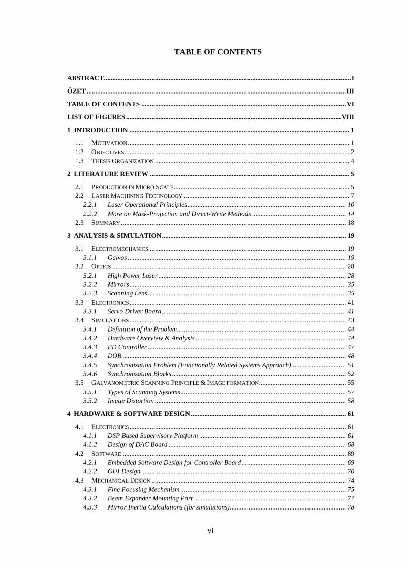
2.2.1 Laser Operational Principles
The “LASER” acronym stands for Light Amplification by Stimulated Emission
of Radiation because for the generation of the laser beam, the principle of stimulated
emission is used [15]. Stimulated emission occurs when an electron is in an excited
state. When a high energy state electron is dropped to a low energy state electron by
passing a photon, the photon with a same wavelength is emitted in the same direction.
The laser medium is necessary to emit a photon by stimulated emission. There are four
different laser mediums such as gas, solid, semiconductor and liquid. Fiber laser is one
of solid-state lasers. On the other hand, CO2 and excimer lasers are the gas lasers. In
general, shorter wavelength of light can generate more energy as shown in the following
equation.
E =𝑐
𝜆
“E” indicates single photon energy, “h” Planck’s constant, “c” the speed of light
and “λ” wavelength of light. Table below shows wavelengths of different lasers and
corresponding photon energies. Decreasing wavelength results with an increasing
energy level as given in the following table.
Table 2.2 Photon energies obtained from different laser sources [16]
Laser Wavelength (nm) Photon Energy (eV)
XeF 351 3.53
XeCl 308 4.03
KrF 248 5.00
KrCl 222 5.50
ArF 193 6.42
𝐅𝟐 157 7.43
There are two main operation modes for lasers, which are continuous wave
mode and pulsed mode. The continuous mode provides continuous energy flow but the
pulsed laser transfers changing output energy depending on pulse duration. On the other

11
hand, pulsed laser mode can reduce the thermal effect during the laser process. A
general laser machine is consisted of three main components which are laser medium,
excitation (pumping) source and reflectors. A laser medium can be various materials,
including gas, solid and semiconductor as mentioned before. Pumping makes the
medium to be in excited state which has high electron energy and the reflectors keep
stimulating the excited electron to emit photons. Figure 2.4 describes the concept and
components of laser machine.
Fig. 2.4 Laser Operation
An important phenomenon for laser technology is ablation. It is characterized by pulsed
removal of small amount of materials from the illuminated region of the target with
minimal damage to the surrounding area [17]. Once the target material absorbs the laser
energy, the material goes through photo thermal (heat induced bond breaking) and
photochemical (bond breaking by photon absorption) processes [18]. Evaluation of
photo thermal (pyrolytic) and (photochemical) photolytic processes has been
demonstrated in the following figure 2.5.

12
Fig. 2.5 Interaction of excimer laser radiation with solids. Right: PVC, photolytic
ablation. Left: metal, melt. Middle: Al2O3 ceramic, combined photolytic
and pyrolytic process [19].
Laser absorption varies depending on the material and the wavelength of laser.
Generally, higher wavelength decreases the laser absorption. Ablation rate is measured
based on Beer’s law. Ablation rate (Ar) can be expressed by absorption coefficient
(αeff), laser fluence (F) and threshold fluence (Fth). When F is larger than Fth, the laser
ablation occurs. Absorption coefficient and threshold fluence rely on the material type
and laser wavelength.
𝐴𝑟 = ln 𝐹
𝐹𝑡
1
𝑎𝑒𝑓𝑓
Following table shows the ablation depth according to laser fluence for several different
materials. It indicates that the ablation depth can vary with the different fluence and the
laser wavelength. Table 2.3 lists ablation depths and fluences of common materials.
Table 2.3 Ablation depths and fluences of materials [15]
Material Wavelength [nm] Fluence [J/cm2] Ablation Depth /
Pulse [μm]
Polycarbonate
(PC)
248 4.0 0.4
Polyester (PES) 248 4.0 0.8
Polyethylene (PE) 193 6.0 4.0
Polyimide (PI) 308 0.3 0.1
Zirkonia 248 10 0.12
Boron nitride 193 20 0.15

13
Piezoelectric
ceramics
248 5.0 0.05
Alumina 193 45 0.06
Silicon carbide 248 10 0.13
The pulse duration is another important factor. Ultra short laser pulses can minimize
photo thermal process during the laser machining so that the higher quality structures
can be obtained with the expense of a higher cost. Comparing different pulse widths
concludes that shorter pulses produce better quality but at higher cost [20].
Especially, melting effects (debris or recast) around the machining areas can be
minimized by short laser pulses. The question what is short and what is ultra short can
be discussed from the viewpoint of the material. The material is subjected to a beam of
photons coming from outside and absorbed in a skin layer. The photons are absorbed in
that skin layer by the free electrons, in about 1 f (10−15) s. The relaxation time of the
electrons is about 1 p (10−12 )s. During that time the energy is stored in the electrons,
and after the relaxation time it is converted into heat. Expressing the intensity of the
incoming beam by 𝐼0, the decrease of the laser intensity depending on the depth can be
found by 𝐼𝑥 = 𝐼0 e−𝛼𝑥 where α is the optical absorptivity of the material and x the depth
into the material. An important quantity is the penetration depth δ (δ = 2/α) in which
almost all laser energy is absorbed. This optical penetration depth is for metals in the
order of 10 nm. It means that the laser energy heats a 10 nm thick layer of metal in 1 ps.
This heat will diffuse from the skin layer to the rest of the material. The diffusion depth
is expressed by d = 4𝑎𝑡 with a as the thermal diffusivity and t the diffusion time. In
case of steel we obtain in 10 fs a diffusion depth of 1 nm while during a 1 ps pulse the
heat diffuses over 10 nm. Moving from these results one consider a pulse as ultra short
when the (thermal) diffusion depth during the pulse is in the same order or less than the
skin layer depth (optical penetration depth). The optical penetration depth depends on
the material and the laser wavelength [21]. In general pulses shorter than 1 ps can be
considered as ultra short.
By using laser micromachining technique, one can create structures not only by
directly fabricating without mask patterns but also by using them [22]. Direct
fabrication process usually provides high flexibility and simple implementation which

14
can be considered as the most valuable advantage of laser machining compared to other
methods. Typically, micro fabrication methods consist of several consecutive processes.
However, laser machining requires only one single process. On the other hand,
supporting high production rate and high resolution structures has been dependent on
whether a mask pattern is used while machining or not; because mask pattern usually
provides high production rate and creates structures with high resolution. However,
more efforts are needed to prepare such equipments. Following figure 2.6 clearly
illustrates both “Direct-Write” & “Mask-Projection” methods.
Fig. 2.6 Illustration of Direct-Write & Mask Projection Methods
2.2.2 More on Mask-Projection and Direct-Write Methods
Vast majority of laser machining systems using the technique of mask
projection, have been based on excimer lasers [23]. This technique is especially suitable
for excimer lasers since their optical properties mean that direct beam focusing may not
be a feasible option and projection methods can be more efficient in the machining of
various micro structures. Such features, which are depicted in for the machining of

15
polyimide, have led to excimer laser systems being used, for example, in the mass
production of ink-jet printer nozzles [24] as previously stated (see Fig. 2.7).
Fig. 2.7 Micro-machining of polyimide to produce ink-jet printer nozzles using excimer
laser mask projection.
In standard mask projection systems, the depth of a micro-structure is controlled
by the number of laser pulses that have been fired and the resolutions of the features are
determined by the mask and the optical projection system. Machining of relatively large
areas (i.e. hundreds of centimeter square) under the same laser beam conditions may be
of concern such that all the micro-structures are engraved to the same depth. This is
something which might be highly desirable in most applications; but in some areas (e.g.
applications including micro-fluidic systems, bio-medical analytical chips and rapid
prototyping [25]) there can be a need to modify the depth of the micro-machined
structures across the sample area.
16
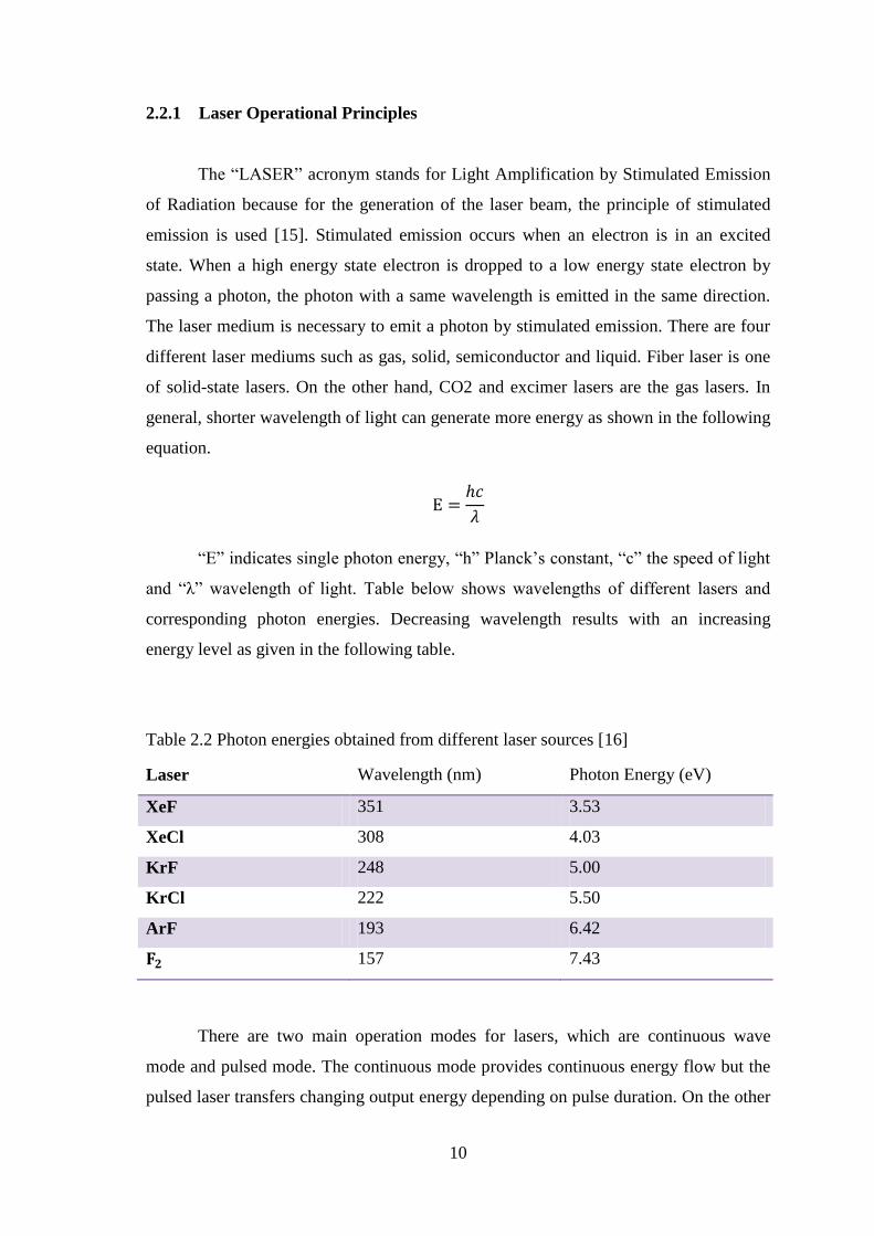
Standard mask projection techniques are very versatile and depth information can be
imparted into micro-machined samples by an appropriate synchronization of the sample
position and the laser firing sequence [26]. The level of control of the depth profile
required in the above-mentioned applications, however, means that these standard
methods do not extend far enough. To overcome this limitation, new techniques such as
synchronized overlay scanning (SOS), has been developed. SOS Technique has been
illustrated in the following figure 2.8.
Fig. 2.8 SOS Technique.
To add depth information, the SOS method additionally shapes the laser beam which is
used and it is the chosen beam shape which determines the depth profile that is imparted
to the micro-structures [27]. The shape of the aperture (i.e. the shape of the beam)
determines the profile of the sample and other features of the SOS method is that the
choice of mask (which determines the features to be made). Below figure 2.9 represents
the typical results obtained.

17
Fig. 2.9 Micro-channels on double ramp.
Solid-state lasers have usually been the preferred light sources in direct writing type of
laser machining applications, mainly due to their high repetition rates (hundreds of
kilohertz), adjustable pulse durations, and variable output power. Since the mechanism
for generating laser pulses lies in the nature of the active laser medium and the
corresponding lifetimes of the atomic energy levels. In that context by using different
pulse generation techniques [28] the pulse duration, pulse energy and reproducibility
can be modified over wide ranges. So that, many applications such as via hole drilling,
solar panel scribing, display panel production and marking and cutting of devices or
products use these lasers. In almost all cases, the technique of direct writing is used.
In direct write systems, the laser beam is focused to a small spot using a lens and either
the beam or the sample (or both) are moved around to produce the desired pattern. In
some cases, additional galvanometer-controlled scanning mirrors are also included. If
scanning mirrors are used, then a flat-field lens is required as this keeps the focal plane
position constant irrespective of the angle of the beam being deflected from the
scanning mirrors (see Fig. 2.10).

18
Fig. 2.10 Flat-field lens in direct-write scanning
Beam spot sizes of a few tens of microns can be achieved with such systems and the
combination of fast scanner mirrors and high repetition rate lasers means that very high
processing speeds can be reached.
Due to the non-availability of a micron level machining mask and related optics in
hand; during the experimental part of this thesis, attention has been concentrated only
on “Direct-Write” method.
2.3 Summary
In this chapter, laser micromachining together with other micromachining techniques
have been introduced, including the basic principles and area of applications. Between
the evaluated methods laser micromachining using direct writing offers a lot of
advantages compared to other fabrication methods. It is an easy to implement, simple
approach and easy to change a process according to different designs.

19
3 ANALYSIS & SIMULATION
3.1 Electromechanics
3.1.1 Galvos
The name “Galvo” stems from the historical Galvanometer, a moving coil instrument
where a mirror was attached to the torsion band of the coil. Such instruments where
used to demonstrate slow varying electric currents. The Galvo scanner use the same
principle however, they are designed for rapid movement of the attached mirror. Instead
of using a torsion band, electromagnetic forces are applied.
Galvo Scanners in modern sense have been widely used in applications such as laser
etching, confocal microscopy, and laser imaging. A galvanometer can be defined as a
precision motor with a limited travel, usually less than 360 degrees, whose acceleration
is directly proportional to the current applied to the motor coils. When current is
applied, the motor shaft rotates through an arc. Motion is stopped by applying a current
of reverse polarity. If the current is removed, the motor comes to rest under friction.
Typically, the term 'Galvo' refers only to the motor assembly, whereas a 'Galvo Scanner'
includes the motor, together with a mirror, mirror mount and driver electronics.
Galvanometer:
The galvanometer consists of two main components: a motor that moves the mirror and
a detector that feeds back mirror position information to the system. Commercial
galvanometers have been supplied also with closed loop circuits to make sure that the
desired position will be reached with high precision.

20
3.1.1.1 Galvo Types and Dynamic Behaviour:
The two main galvo types in terms of the electromechanical structure can be ordered as
“moving coil” and “moving magnet” type. Following part covers these configurations
and their dynamic behaviour.
Moving Coil:
The basic idea in that configuration is to exploit electromagnetic forces to generate an
angular motion. For this purpose a moving coil is placed inside a permanent magnet. By
means of a spiral spring which is fixed to the axis the electrical current is supplied to the
moving coil. The same arrangement is attached to the bottom side of the coil. Beside the
transport of the electrical current to the coil the spiral springs are also used to balance
the electromagnetic forces that appear when the current is flowing through the coil
against its restoring force. Conventional moving coil arrangement has been depicted in
Fig. 3.2.
From the basics of electromagnetically phenomena we know that a current flux j always
generates a magnetic field H like:
∇ × 𝐇 =𝜕𝑫
𝜕𝑡+ 𝑗
Since we consider here only conductors we can neglect the displacement field D. From
the equation above we conclude that a linear current flux density which is present in a
straight conducting wire generates a curled magnetic field as shown in Fig. 3.1 However
if the currents flow in a curled conductor as it is the case for the coil then the generated
magnetic field becomes linear.
Fig. 3.1 Linear current flux generates a curled magnetic field and a curled flux generates
a linear one

21
In the moving coil instrument the current flows in a curled manner thus generating a
linear magnetic field H or magnetic flux density B. The superposition of the magnetic
fields generated by the current flux and the permanent field results in a torque T of the
moving coil:
T = N A I B
whereby N is the number of turns in the coil, A the area of the cross section of the coil,
I the current flowing through it and B the magnetic flux density inside the gap. The
torque T tries to turns the coil in such a way that the overall magnetic flux density
becomes a maximum. However the spiral springs are generating a restoring torque (see
Fig 3.2) Tr which goes linear with the angular deflection α, i.e.
Tr = c α
Whereby c is the spring constant or a material property of it. The equilibrium is reached
when both torques have the same value:
T = Tr → α =N ⋅ A ⋅ B
c ⋅ I
From the equation above it can be seen that the deflection angle α is proportional to the
current I flowing through the coil.
Fig. 3.2 Conventional Moving coil arrangement

22
To demand that the mirror follow fast variations of the current one has to consider the
dynamics of the system. In a first approximation the system consists of a mass and a
spring which is driven by an external force.
Θ ⋅𝑑2α
𝑡2 + k ⋅
𝑑α
𝑑𝑡+ c ⋅ α = K0 ⋅ cos ω ⋅ t
inertial + friction + restoring = driving torque
The equation above represents the differential equation for forced oscillation.
Depending on the individual parameters as inertial moment, frictional (k) and restoring
constants (spring constant c) such a system operates in four different modes:
1. Resonant mode
2. Damped oscillation
3. Maintained oscillation
3. A periodic mode
Depending on the value of the relative damping factor γ:
γ =k
Θ ⋅ c
From a proper scanner, what is usually expected is that, it follows the variation of
current I with highest possible speed. This can be achieved in the beginning of the
periodic domain (critical damping), which means a short and small over shooting of the
desired mirror position occurs. For this case the following equation must be true:
k = 2 ⋅ Θ ⋅ c or γ = 2
However, in this mode the amplitude decreases with increasing frequency. To extend
the range - while also preventing the amplitude to drop too much at high frequencies -
the resonance frequency ωR of the system:

23
ωR = c
Θ−
𝑘2
Θ2
should be designed as high as possible. This can be achieved by reducing the friction (k)
or the inertia moment of the rotating coil. That actually means the mass of the coil must
be reduced. But here we are faced with the problem that reducing the mass finally
means reducing the mass of the used conductor. For this reason instead of copper,
aluminium can be used. Therefore in more advanced systems, moving magnets are used.
This has the advantage that no electrical connections to the moving part are required
and furthermore it lifts the limit of maximum power that can be introduced into a
moving coil.
One has to consider that the current flowing through the coil - besides the magnetic field
- produces heat due to power P = I2R where R is the resistance of the coil. The coil is
moving inside an air gap and after vacuum; air is the worst thermal conductor. The only
real heat sink for the coil is the pick-off structure. Therefore the heat is mainly
dissipated by convection to the pole pieces. Consequently the main failures of moving
coil scanners become prominent as the coil burn out and degradation of the permanent
magnet. The two major problems that the performance of such scanners suffer from:
1. The thermal limit defined by the heat transfer capabilities of coils and the Curie
temperature of the magnet
2. The coil creep and deformation of the coil under centrifugal acceleration
A moving magnet system can solve the problems of both burn out and magnet
degradation. The principle of such a system is shown in Fig. 3.3.
Moving Magnet:
Galvos in that configuration contains a moving magnet, which means that the magnet is
part of the rotor and the coil is part of the stator. This configuration provides faster
response and higher system-resonant frequencies when compared to moving coil
configurations. Mirror position information is provided by an optical position detector,
which consists of two pairs of photodiodes and a light source. As the galvo and mirrors

24
are moved, differing amounts of light are detected by the photodiodes and the current
produced is relative to the galvo actuator position.
Fig. 3.3 Moving magnet arrangement
A permanent magnet (MM) is placed in the centre of two pole pieces which are supplied
with two coils W1 and W2 which are thermally connected to the housing. High torque
and high duty cycles, however, still require proper heat sinking to avoid thermal
overload. A proper design of the magnet guarantees consistent properties beyond 135
°C (see Fig. 3.4). Compared to moving coil systems this arrangement can accommodate
three times the power dissipation of equivalent inertia and torque constant. A spindle is
attached to the magnet which is fixed in position by means of two ball bearings (B).
Instead of using a mechanical spring a servo loop with a position sensor (AE) and
controller is used.
Fig. 3.4 Technical realization of a moving magnet scanner
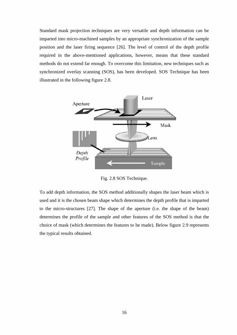
In the arrangement of Fig. 3.5, a cylindrical permanent magnet (1) is used. Since the
inertia of a solid cylinder is given by:
25
Θcyl =1
2𝑚𝑟2 =
1
2ρ ⋅ π ⋅ L ⋅ 𝑟4
Usually a cylinder which has a length that is larger than the radius has been used to
obtain the smallest possible inertia.
Fig. 3.5 Inertias of cylinders
Permanent rotor magnets for scanners are manufactured from an alloy of Neodymium,
Iron and Boron. This compound allows the manufacturing of very strong magnets. A
small air gap is between the magnet and the coils (2) which are wound around the pole
pieces of the flux return piece (3). The housing (4) is also used as heat sink.
3.1.1.2 Critical Parameters in Selection of Galvos:
That part tries to cover the evaluation of some parameters that has been handled
as critical in the selection of galvo modules.
In laser machining applications, optical energy level that is required to
implement a certain type of processing job may vary depending on the work piece’s
material properties and other factors such as physical size and geometry as well as the
application itself. Laser on time and optical output power both together, determine the
amount of energy affecting on the work piece hence also the overall processing time. So
an increase in the number of work pieces or amount of material to be machined might
cause a growth in overall processing time which might be costly in some cases (i.e.:
mass production). Considering the latest developments and technological tendencies of
high-end industrial solutions in the market, lasers that offer nanosecond or picosecond
level of pulse operation times have been of concern. Shortening the pulse on time
typically provides the ability to use higher peak power levels and that also contributes to

26
faster operation. In that context other elements -such as beam guiding elements- related
with those kind of systems should also be of a fast response type having actuators that
can move relatively fast. So electromechanical systems integrated in such systems
should also have high enough operational bandwidth. Since reaching to high
accelerations and velocities might be necessary most of the time, galvanometric scanner
modules which have widely been used in those applications have typical bandwidths
around hundred hertz for full scale, large angle (±20°) and can reach up to 1kHz for
small angle (±0.2°) motion. In most electromechanical systems, maximum achievable
acceleration and velocity values for the motion has usually been limited by actuators’
inertia. In that sense, inertia can be seen as an obstacle or kind of a disturbance that
influences the system for high acceleration values and velocities. Due to the nature of
the optical based scanning applications, used electromechanical actuators and other
moving elements (i.e.: reflective surfaces/mirrors mounted on galvo rotors) should have
low inertias to eliminate the undesired disturbances on the system motion and have fast
scanning action and dynamic response. In addition to those, most of the industrial
control applications require the use of a closed loop control techniques obtain the
desired operational performance.
Most laser machining applications such as laser drilling, cutting, scribing and
specifically applications such as laser micromachining, micro engraving, silicon wafer
processing, medical equipment processing (i.e.: stent fabrication) requires relatively
higher accuracy, compared to the conventional industrial control applications therefore
accuracy of motion and precision levels has been critical issues.
Resolution has been another important parameter in identifying the performance of the
material processing application systems. Assuming a target motion of micron levels;
resolution of few hundred nanometers or higher has usually been considered as
acceptable. Resolution level has mainly been decided depending on the step resolution
of the used position detection systems (i.e.: rotary or linear optical encoders).
Stated SPI Laser platform has a beam diameter around 10mm, so the selected galvo
system should have mirrors with appropriate size to be able to properly guide the laser
beam on the projection surface. Also these reflective surfaces should have desired level
of reflectivity (usually provided with special coatings) for target wavelengths and
should absorb as little optical power as possible.

27
In most of the control applications, it has been expected that the driver/controller block
for the actuators should have control input signal compatibility to provide adaptability
with existing control interfaces/systems.
Due to the relatively high levels of precision aimed in micromachining applications,
non-switching linear control signals have been more preferable rather than high speed
switching, modulated signals; because non-switching drive techniques usually provides
lower electrical noise therefore allowing higher control accuracies.
Under the guidelines of the above stated parameters; Thor Labs’ GVS012 2-axis
Galvanometric Scanner modules have been chosen for the studies.
GVS012 Modules:
Thorlabs’ GVS Series of Scanning Galvanometer Mirror Systems can be classified as
high-speed mirror positioning systems designed for integration into OEM or custom
laser beam steering applications. GVS012 modules have been depicted in the following
figure 3.6.
Fig. 3.6 Dual-axis Galvo Modules

28
Modules have the following fundamental features:
Moving Magnet Motor Design for Faster Response
High-Precision Optical Mirror Position Detection
Analog PD Control Electronics with Current Damping
and Error Limiter
Protected Silver Mirror Coating
Dual-Axis System for <Ø10 mm Beams
The system includes a dual-axis galvo motor and mirror assembly, together with
associated driver cards and driver cards’ heat sinks. GVS012 systems also include a
base plate, which is a combined post adapter and tilt platform adapter. Use of a low
noise, linear PSU has been recommended by the manufacturer to get the full
performance from the modules.
GVS012 galvo consists of a galvanometer-based scanning motor with an optical mirror
mounted on the shaft and a detector that provides positional feedback to the control
board. The moving magnet design for the GVS series of galvanometer motors has been
chosen over a stationary magnet and rotating coil designs in order to provide the faster
response times and the higher system resonant frequency. The position of the mirror is
encoded using an optical sensing system located inside of the motor housing. As
previously mentioned, due to the large angular acceleration of the rotation shaft; size,
shape and inertia of the mirrors become significant factors in the design of high
performance galvo systems. Furthermore, the mirror must remain rigid (flat) even when
subjected to large accelerations. All these factors have been evaluated in the selection of
galvo system in order to match the desired characteristics and maximize performance.
3.2 Optics
3.2.1 High Power Laser
3.2.1.1 Understanding Laser Features & Parameters:
Besides power or energy level of a laser source, there are other parameters that
are still critical in terms of operational performance of the module. Among them, beam

29
diameter (or radius), spatial intensity distribution (or profile), divergence and the beam
quality factor (or beam parameter product) can be handled as the most prominent ones.
In many applications, these parameters may define success or failure and, therefore,
their optimization seems to be crucial.
Beam Diameter (Radius, Width):
The beam diameter can be thought as the most important propagation-related property
of a laser beam. In case of a perfect flat-top profile the beam diameter is clear but most
laser beams have other transverse shapes or profiles (for example, Gaussian) in which
case the definition and measurement of the beam diameter is not trivial.
The boundary of arbitrary optical beams is not clearly defined and, in theory at least,
extends to infinity so that a commonly used definition of the beam diameter is the width
at which the beam intensity has fallen to 1/e² (13.5%) of its peak value. Other common
definitions of the beam diameter are the full width at half-maximum (FWHM) diameter
or the diameter that includes 86% of the beam energy. Many lasers exhibit a significant
amount of beam structure, and applying these simple definitions leads to problems.
Therefore, the ISO 11146 standard specifies the beam width as the 1/e² point of the
second moment of intensity, a value that is calculated from the raw intensity data and
which, for a perfect Gaussian Beam, reduces to the common definition.
Spatial Intensity Distribution (Beam Profile):
The spatial intensity distribution of a laser beam combines all the mechanical, thermal
and electromagnetic variables that created the beam. The way that the power has been
distributed across a laser beam depends on both the mode or combination of modes
running in the laser cavity and on how those modes are distorted by the presence of
apertures, refractive index of optical elements used, imperfect optical surfaces and other
perturbing effects. Therefore, spatial intensity distribution is one of the fundamental
parameters which indicate how a laser beam will behave in an application.

30
Divergence:
The beam divergence of a laser beam is a measure for how fast the beam expands as it
propagates in space. According to a common definition, the beam divergence is the
derivative of the beam radius with respect to the axial position in the Far Field. This
definition yields a divergence half-angle, and further depends on the definition of the
beam radius (or, diameter). Sometimes, full angles are used which results in twice as
high angles. Beams with a very small divergence, i.e. with an almost constant beam
diameter over a significant propagation distance are generally called “collimated
beams”.
Beam Quality Factor M² (Beam Parameter Product):
The beam quality factor M² is derived from the uncertainty principle. The factor is
shown to describe the propagation of an arbitrary beam. M² is a measureable quantity in
order to characterize real mixed-mode beams. For example, the angular size of a non-
Gaussian laser beam in the Far Field will be M² times larger than calculated for a
perfect Gaussian beam. In other words, M² describes how close to “perfect-Gaussian” a
laser beam is. For a perfect Gaussian beam, M² is 1. For a non-prefect Gaussian beam,
M² is >1. See following figure 3.7.
Fig. 3.7 Laser Beam Quality
31
3.2.1.2 Technical Details:
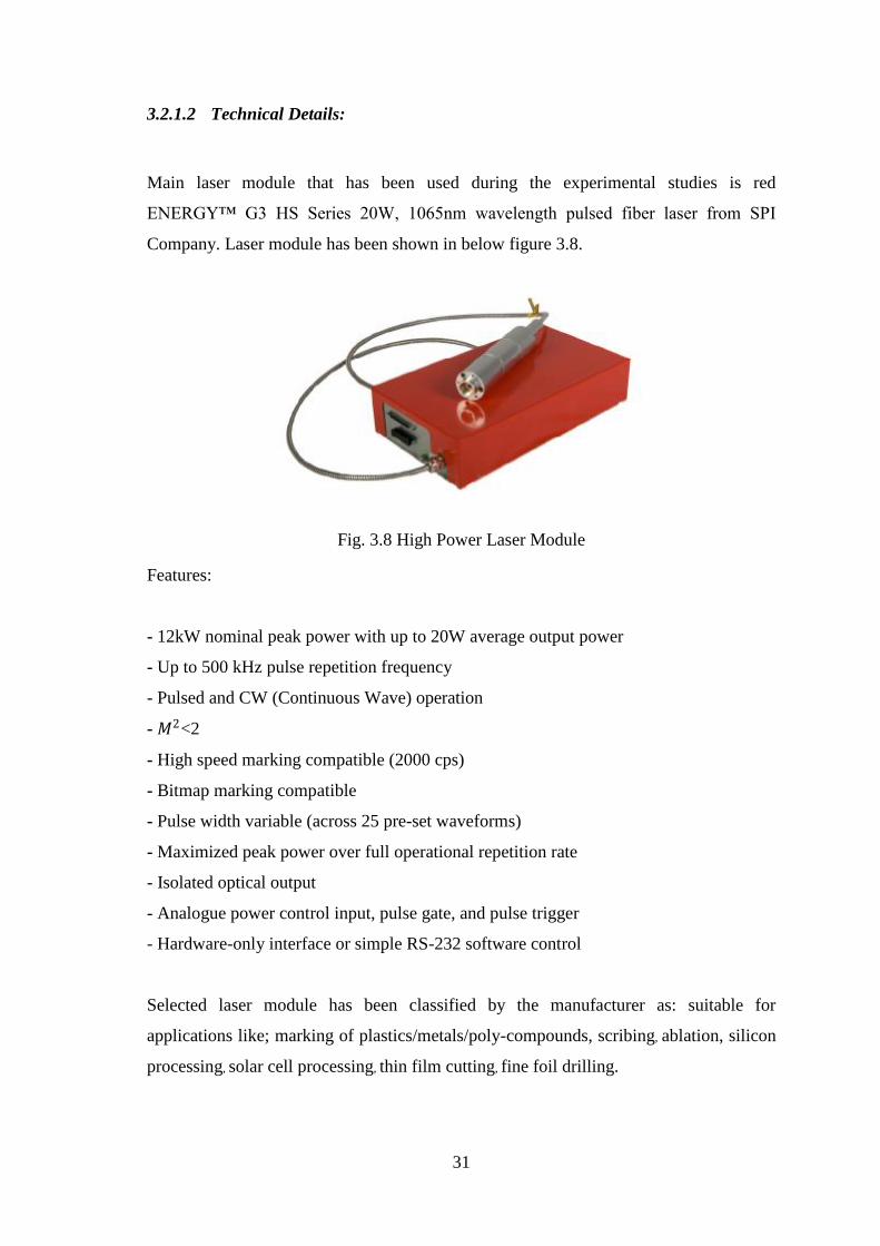
Main laser module that has been used during the experimental studies is red
ENERGY™ G3 HS Series 20W, 1065nm wavelength pulsed fiber laser from SPI
Company. Laser module has been shown in below figure 3.8.
Fig. 3.8 High Power Laser Module
Features:
- 12kW nominal peak power with up to 20W average output power
- Up to 500 kHz pulse repetition frequency
- Pulsed and CW (Continuous Wave) operation
- 𝑀2<2
- High speed marking compatible (2000 cps)
- Bitmap marking compatible
- Pulse width variable (across 25 pre-set waveforms)
- Maximized peak power over full operational repetition rate
- Isolated optical output
- Analogue power control input, pulse gate, and pulse trigger
- Hardware-only interface or simple RS-232 software control
Selected laser module has been classified by the manufacturer as: suitable for
applications like; marking of plastics/metals/poly-compounds, scribing, ablation, silicon
processing, solar cell processing, thin film cutting, fine foil drilling.

32
The device is technically described as a DC-powered laser module built around a dual-
stage Yb doped fiber amplifier system with an optical seed pulse generated by a single-
mode semiconductor laser diode. These amplifiers are pumped by multi-mode laser
diodes with wavelengths around 900nm. Fiber beam delivery is done from a fiber-optic
beam delivery cable that is terminated with a beam collimator, optical isolator, and
beam expander. The module contains drive electronics for the diodes, amplifiers and
synchronization of the optics with the user set parameters (see Fig 3.9).
Fig. 3.9 Functional block-diagram of the Laser Module
Laser module can be controlled by using either one of three different methods:
-Basic Hardware Control
-Extended Hardware Control
-Software Control
3.2.1.3 Laser Control:
The main philosophy behind the designed controller board was targeting a highly
functional but also compact design that will make the system integration easy; serving
to that purpose instead of using parallel communication methods which usually includes
many data lines hence also many other potential that might occur due to the high
number of wirings-connections; it uses serial communication methods to communicate
with most of the peripherals.

33
So that with the exception of a few control features, software communication method
has been used for the control of high power laser. That mode supports many functions
that can be accepted as fundamental for the target experimental work and most future
work.
Following figure 3.10 summarizes the main functions supported by different modes.
Fig. 3.10 Control Availability and Implementation
As can be observed from the table, some features such as “Laser Emission Gate
Control”, “Laser Disable” must be controlled by using digital connections. In addition
to that, optional hardware control of the global enable pin may provide convenience in
some cases. So as a solution, some pins in the PWM output port of the controller board
has been reserved for the control of those lines. Using dedicated PWM outputs ports has
advantages in the cases where duty cycle based control might be necessary (e.g.
modulation of the laser emission gate to be able to adjust the output power in an
alternative manner).
Different applications or working with different materials might require setting of laser
output parameters such as output power level, pulse burst length, pulse repetition rate,
34
pulse duty factor). These parameters can be adjusted by using the related commands
(see Appendix D). For example below figure 3.11 exhibits the change in output pulse
shapes depending on the selected waveform and pulse repetition frequency.
Fig. 3.11 Examples of Optical Pulse Shapes
One can observe that the relation exhibited in the above plot between pulse time and
pulse energy level is as seen in the following figure 3.12.
Fig. 3.12 Illustration of average power / pulse energy variation with PRF

35
3.2.2 Mirrors
The mirror assembly is attached to the end of the actuator, and deflects the light beam
over the angular range of the motor shaft. Scanning galvo applications demand high
speeds and frequencies of the shaft rotation, so that the inertia of the actuator and mirror
assembly can have a profound effect on the performance of the system. High resonant
frequencies and enhanced stiffness in the mirror assembly also add to system
performance by increasing bandwidth and positively affecting response times. The
mirrors that have been used, have protective silver-coating (see Appendix C) and are
suitable for applications from 400nm up to near infra red (2000nm), and can tolerate
powers around 100 to 150W/cm2.
3.2.3 Scanning Lens
Galvanometric scanning based laser machining applications require the use of special
optics to improve the processing quality and performance by decreasing the image
distortion due to scanning action and increasing the resolution. This type of objective
lens is usually called a scan lens because a laser beam is scanned across the back
aperture of the objective lens in order to form the image of the sample. Each position
that the laser is scanned over corresponds to one point in the image formed. This
approach results in a focal spot on the sample that is not, in general, coincident with the
optical axis of the scan lens. In traditional lenses, this would result in the introduction of
severe aberrations that would significantly degrade quality of the resulting image.
However scan lenses were designed to create a uniform spot size and optical path length
for the laser for every scan position, which allows a uniform, high-quality, image of the
sample to be formed.
When designing an imaging system that uses a scan lens, it is important to
accommodate the Design Wavelength, Parfocal Distance, Scanning Distance, Entrance
Pupil, and Scan Angle specifications in order to maximize the image quality (see Fig.
3.13). For imaging systems with a single galvo mirror the center of the objective's
entrance pupil must be coincident with the center of the galvo mirror. If the imaging
system uses two galvo mirrors (as in our case) then the entrance pupil should be located
between the two galvo mirrors. It is important to minimize the distance between the two

36
galvo mirrors, because when the entrance pupil and beam steering pivot point are not
coincident, the quality of the image is degraded. This is principally due to the variation
in the optical path length as the beam is scanned over the sample. Drawings for an
imaging system containing two galvo mirrors have been given in following figure 3.13.
Fig. 3.13 Entrance Pupil in 2-axis Scanning System
Considering the requirements of the application, LSM02-BB (Broad Band) telecentric
scan lens have been selected from Thor Labs Company.
3.2.3.1 LSM02-BB Lens Technical Features:
Features
Constant Magnification Over Entire Field of View (FOV)
Constant Spot Size
Flat Image Plane
Excellent Coupling Efficiency
Large Field of View
EFL (Effective Focal Length)= 18mm
WD (Working Distance)= 7.5mm

37
Scan Lens Thread: M25 x 0.75
The LSM series of scan lenses are telecentric objectives that have been classified as
ideal –by the manufacturer- for use in laser scanning applications. Those telecentric
objectives are used in laser imaging systems because of the advantages of a flat imaging
plane when used in applications that scan the laser across the sample being processed. A
flat imaging plane minimizes image distortion, which in turn allows for the creation of
geometrically correct images without the need for extensive post image processing. In
addition, the spot size in the image plane is nearly constant over the entire FOV (see
figure 3.14 Scan Lens Plot) so that resolution of the image is constant.
Fig. 3.14 Scan Lens Plot
A very important factor in micromachining applications is the final spot size
after focusing. Following equation can be used to estimate theoretically allowable
diffraction limited minimum spot size:
𝐷𝑚𝑖𝑛 =4𝜆𝑓𝑀2
𝜋𝐷𝑜
Ex: Getting 𝜆(𝑤𝑎𝑣𝑒𝑙𝑒𝑛𝑔𝑡) = 1064 𝑛𝑚, 𝑓 𝑒𝑓𝑓𝑒𝑐𝑡𝑖𝑣𝑒 𝑓𝑜𝑐𝑎𝑙 𝑙𝑒𝑛𝑔𝑡 = 17.97 𝑚𝑚,
𝐷𝑜 (input beam diameter) = 9.1mm, 𝑀2(beam quality factor) = 2 𝐷𝑚𝑖𝑛 = 5.35 µm
For the telecentric lens used, due to the minimum level wavelength and scan angle
dependency of the spot size and lens specs, it is around 15 um for most values of the
scan angle and wavelength.
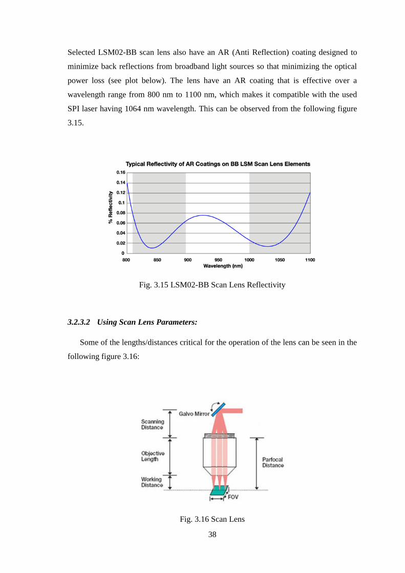
38
Selected LSM02-BB scan lens also have an AR (Anti Reflection) coating designed to
minimize back reflections from broadband light sources so that minimizing the optical
power loss (see plot below). The lens have an AR coating that is effective over a
wavelength range from 800 nm to 1100 nm, which makes it compatible with the used
SPI laser having 1064 nm wavelength. This can be observed from the following figure
3.15.
Fig. 3.15 LSM02-BB Scan Lens Reflectivity
3.2.3.2 Using Scan Lens Parameters:
Some of the lengths/distances critical for the operation of the lens can be seen in the
following figure 3.16:
Fig. 3.16 Scan Lens

39
As previously mentioned; for ordinary lenses, beam position in the FOV (Field of
View) depends on the “tangent of the scan angle”; whereas on the other hand telecentric
lenses and F-theta lenses have no tangent of the angle dependency; but instead beam
position directly depends on the angle.
Following figure 3.17 represents output pattern of an F-theta lens with telecentric
behaviour for a typical dual-axis galvo system:
Fig. 3.17 Scan Lens
(*) “Partial” F-theta nature of the selected lens can be understood by using the
following relations:
-Overall scan angle θmax refers to the maximum diagonal scan angle
-The scan length can be calculated with the formula:
2γ= EFL x 2 x θ x π/180
Example: For LSM02–BB scan lens specs given in table (see Appendix A) “θ” scan
angle= 7.5 degree; “EFL” (Effective Focal Length) = 17.97 mm (around 1050 nm
wavelength)

40
FOV= 17.97*2*7.5* π /180 solving the equality
FOV= 4.704534 mm also matches with the given 4.7 mm x 4.7mm FOV
parameter
Note: π/180 is conversion factor from degrees to radians
Assuming full utilization of the given 4.7 mm x 4.7 mm area and a focused beam spot
size of 23.5 um (worst case scenario) 4.7mm/23.5um = 200 spot workspace are in
each axis, which is equivalent to 200 x 200 spot based resolution. That value can be
considered as acceptable for most machining purposes.
(*): The word “Partial” is due to slight differences between focusing behaviour of
telecentric and F-theta lenses in terms of focused beam’s angle of incidence. This can be
observed from the following figure 3.18:
Fig. 3.18 F-Theta & Telecentric
The problem with the simplest type of F-theta lens is that the focused beam hits the
work piece at an angle, causing an elliptically shaped focused spot which may have to
be taken into consideration in some applications. For surface treatment applications,
such as marking, this may not be a problem; however for material removal applications,
such as hole drilling, this can be an issue (unless a hole slanted with respect to the
surface is desired). In a telecentric lens, the exit beam from the optical system is
perpendicular to the work surface over the entire field of view. This solves the problem
just described. However, it necessitates having a lens which is at least as large
physically as the scan field that can increase optical system costs.

41
3.3 Electronics
3.3.1 Servo Driver Board
As previously stated, galvos have their dedicated driver&controller stages based on
servo drive structure. The servo circuit interprets the signals from the position detector,
then uses positional error, speed and integral of current terms to output control voltages
to drive the actuator to the demanded position. The scanner uses a non-integrating,
Class 0 servo, which enables higher system speeds compared to integrating servo
systems, and can be thought as ideal for use in applications that require vector
positioning (e.g. laser marking) or raster positioning (printing or scanning laser
microscopy). It can also be used in some step and hold applications. The proportional
derivative circuit gives acceptable dynamic performance and includes an additional
current term to ensure stability at high accelerations. The figure 3.19 below shows the
architecture of the driver in more detail.
Fig. 3.19 Servo Driver Board Schematic Diagram
Here considering the additional current term integrated and fed to the system, that block
in a sense behaves like a disturbance observer structure. Further information will be
given in “3.4 Simulations” Section.

42
Fig. 3.20 Servo Driver Board
In the figure 3.20 above, it can be seen the general view of a driver board for a single
axis. Both X-axis and Y-axis galvos have their dedicated servo drivers. Depending on
the measurements made on the X and Y galvos, their electrical characteristics can be
considered almost as identical:
Table. 3.1 Galvo Module Electrical Characteristics
X Galvo Y Galvo
Rc (Coil Resistance) 2.49 Ohm 2.50 Ohm
Lc (Coil Inductance) 166uH 168uH
Note: Measurements have been done with an Agilent U1731A LCR meter.
So one can expect the drivers can be used interchangeably; but due to the differences in
size, geometry and the inertias of the mirrors mounted on the rotors, each galvo should
be used with its matching, calibrated driver. Galvos have been used with the factory
default settings, without making additional adjustments or tuning; with the exception of

43
enabling of the onboard notch filter located at the input of the power amplifier stage, to
eliminate the hissing type high frequency noise.
Each driver board requires the use of a split power supply. Power supply output voltage
can be between ±15V - ±18V. Drivers have on board signal connections for position
sensor currents (e.g. Position Sensor A Current, Position Sensor B Current, motor coil
drive signals). Driver boards support either single-ended or differential mode operation;
first one providing ease of use while the latter one making higher common mode
rejection ratios achievable. Driver boards can be enabled by using an external control
signal but there is no such option for disabling or bypassing the on board controller
which might be considered as a handicap for control applications. Low output
impedance +12V, -12V output
In addition to all those a separate on board connector provides diagnostic information
for:
-Scanner Position
-Internal Command Signal (*)
-Positioning Error x 5
-Motor Drive Current
-Test Input (NC)
-Motor + Coil Voltage / 2
(*)= Internal command signals produced by the controller stages can be observed
externally; but that control signals can not be modified (e.g. changed or added or
subtracted) without making additional modifications on the board physically; that is
why flexibility of control has been limited with the drivers’ built-in control features.
3.4 Simulations
Main focus of the simulation studies can be summarized as: to get familiar with
the dynamic behaviour of the galvo modules and better understand the effect of the
internal/external disturbance(s) on the position tracking performance of the galvos.

44
3.4.1 Definition of the Problem
In terms of the relative motion of the laser beam and work piece during the laser
micromachining process; procedure can be classified in three main categories:
a) Laser beam moving, work piece stationary
b) Laser beam stationary, work piece moving
c) Laser beam moving, work piece moving
Simulation work, tries to concentrate on the case “a)”, in which only laser beam
moving and work piece assumed as stationary. Main reason for choosing this approach
is that, it reflects the existing scenario in the real world experiments, best. In that
context synchronization between galvos might be an important control challenge to
better observe how differences in galvo characteristics act on the dynamic behaviour of
the modules especially when acceleration values are high as it might be the case in
raster type of scanning applications. So this part focuses on the synchronized control
model of a dual-axis galvo system, and elimination of differences such as inertial
differences (e.g. due to the different mirror geometry, electrical characteristics) using
related control structures.
Methodology:
Overall methodology can be summarized as first understanding the structure of
the reference hardware (galvos, controller board), than mathematically modeling and
simulating the proposed synchronization approach in Simulink environment.
3.4.2 Hardware Overview & Analysis
Plant:
As stated previously, galvos of the GVS012 system have moving magnet DC motor
structure, thus can be driven either in a voltage controlled or a current controlled
manner. When the electronic hardware overviewed, an onboard audio class power
amplifier that uses the current output driving configuration and related current

45
measurement features have been observed. Since the control input to the driver board is
taken as voltage reference; additional mathematical transformation - scaling factors can
be used to convert voltage reference input to desired position reference value.
Driver & Controller Block:
The evaluation of that block is as it has been given in the Servo Driver Board
subsection of the Electronic Elements section.
Under the guidelines of those analyses, a corresponding plant and controller model have
been implemented in Simulink.
Math Model:
Here instead of directly concentrating on synchronization we begin with single axis
galvo control. Proposed control scheme has been given in the following figure 3.21:
Fig. 3.21 Proposed Scheme
Double integrator plant part can be thought a suitable mechanical representation for a
brushed DC galvo motor; 𝜏𝑒𝑥𝑡 showing the external disturbances (such as load inertia);
𝜏𝑑𝑖𝑠 as total disturbance effect due to both internal (rotor inertia, friction, coil-armature
resistance…) and external effects.
Controller part is formed of a “feedback term” PD Controller and a “feed forward
term” . term is expected to decrease transient times so that dynamic
response of the system (i.e.: to a step input) can be further enhanced.

46
The part named “disturbance evaluation” can be thought as the block that provides the
previously stated “additional current term” which might be required to suppress reaction
torque (i.e. caused by rotating mirrors) that may occur due to the inertia at high
acceleration values. It also helps minimizing the effects of the disturbances on the
system.
Plant:
Fig. 3.22 Plant Model
After analyzing the related hardware, plant internal structure has been selected as a
double integrator configuration (see Fig. 3.22), which later by control internal dynamics
have been canceled out so that desired position reference tracking operation can be
implemented. When formed as below; given a current input, a position output is
produced by the plant. To realize a more realistic plant model, disturbance effects (e.g.
inertia values calculated previously) can be applied to the system through the
“LoadInertia_Effective” input. See following figure 3.23.
Fig. 3.23 Plant Simulink Model

47
3.4.3 PD Controller
Considering the proposed control scheme above, PD controller (see Fig 3.24) can be
thought as the “feedback based” convergence term of the control so that error dynamics
have been enforced to zero in a closed loop.
Fig. 3.24 PD Controller
Basic functionality of the PD block, for different “kp” and “kd” values can be seen from
the following figures:
Fig. 3.25 -Step Response for “10” (PD Control kp=100 kd=10)
(Horizontal axis: time ; each slot represents 1 second)

48
Fig. 3.26-Step Response for “10” (PD Control kp=160 kd=140)
(Horizontal axis: time ; each slot represents 1 second)
3.4.4 DOB
To be able to represent the controller features of the hardware better, a DOB having a
first order low pass filter structure have been used. Below can be seen the DOB
structure used in simulations. It takes the torque applied to the system (labeled as
“DOB_torq_in”) and measured angular velocity (DOB_w_in) as known inputs. Output
of the observer is the estimated disturbance torque (DOB_torq_out) which has later
been fed in to the plant after being transformed to an additional current term to
minimize the effect of the disturbances on the system. Considering the measured
variables on the electronic hardware, each known input used in the observer block can
be derived from a related measurement on the controller board, so that proposed
observer can be thought as an appropriate alternative to the specific part of the existing
hardware. Proposed DOB structure and operational performance has been depicted in
the following figures.

49
Fig. 3.27 DOB Structure
Fig. 3.28 Sample DOB outputs for “5” and “0.001+ 0.000001*sin(2*pi)”
(Horizontal axis: time ; each slot represents 0.01 second)
For given disturbances at plant input, proposed DOB structure gives the expected
estimation values for constant or slowly varying inputs, independent of the amplitudes.
The transient delay observed at the beginning of the estimation is due to the filter
structure of the observer. That corresponds to less than 10 samples for a simulation step
of 0.001s.

50
Feed forward Term:
Following figure clearly shows that transient time is decreased after additional
term which is obtained by double differentiation of the position reference input.
Fig. 3.29 Transient Response for “10” (PD Control kp=125 kd=20)
(Horizontal axis: time ; each slot represents 0.002 second)
Initially no disturbance has been applied to the plant, to better observe the difference in
the transient response time (see Fig. 3.30):
Fig. 3.30 PD Controller and Observer (no disturbance)

51
Fig. 3.31 Transient Response for “10” (Feed Forward + PD Control kp=125 kd=20)
(Horizontal axis: time ; each slot represents 0.001 second)
3.4.5 Synchronization Problem (Functionally Related Systems Approach)
In terms of control synchronization problem of two galvos can be handled as two
systems tracking the same reference. We can start by making error definitions such that
the control problem has been transformed into a new one in which it will be
implemented using sum and difference of the initial terms. If both plants succeeds to
track the given reference than at the end we should have two systems tracking the same
reference such that their sum should be qref+qref=2*qref and difference is qref-qref=0
and when back transformed to the initial terms, the desired unique controls can be found
[32].
Error definitions:
𝑒𝑐 = 𝑞𝑐 − 𝑞𝑐𝑟𝑒𝑓
= 𝑞𝑐 − 2𝑞𝑟𝑒𝑓
𝑒𝑑 = 𝑞𝑑 − 𝑞𝑑𝑟𝑒𝑓
= 𝑞𝑑 − 0
Generalized errors can be written as:
𝜎𝑐 = 𝑐𝑞𝑐 + 𝑐1𝑞 𝑐 − 2(𝑐𝑞𝑐𝑟𝑒𝑓
+ 𝑐1𝑞 𝑐𝑟𝑒𝑓
)

52
𝜎𝑑 = 𝑐𝑞𝑑 + 𝑐1𝑞 𝑑 − 0
By using the generalized error definitions above exponential convergence can be found
using
𝑞 𝑖𝑐𝑜𝑛 = −𝑘 𝜎𝑖
2𝛼−1sign 𝜎𝑖 ,1
2< 𝛼 < 1
The derivative of the generalized errors when evaluated at 0 gives equivalent control
terms
𝑞 𝑐𝑒𝑞 = 2 𝑐𝑞 𝑐
𝑟𝑒𝑓+ 𝑞 𝑐
𝑟𝑒𝑓 − 𝑐𝑞 𝑐
𝑞 𝑑𝑒𝑞 = 0 − 𝑐𝑞 𝑑
Sum of convergence and equivalent control terms gives the desired control:
𝑞 𝑐𝑑𝑒𝑠 = 𝑠𝑎𝑡 𝑞 𝑐
𝑒𝑞 + 𝑞 𝑐𝑐𝑜𝑛
𝑞 𝑑𝑑𝑒𝑠 = 𝑠𝑎𝑡 𝑞 𝑑
𝑒𝑞 + 𝑞 𝑑𝑐𝑜𝑛
And after the final transformations:
𝑞 𝑚𝑑𝑒𝑠 =
𝑞 𝑐𝑑𝑒𝑠 + 𝑞 𝑑
𝑑𝑒𝑠
2
𝑞 𝑠𝑑𝑒𝑠 =
𝑞 𝑐𝑑𝑒𝑠 − 𝑞 𝑑
𝑑𝑒𝑠
2
3.4.6 Synchronization Blocks
a) General view of the synchronization model:

53
Fig. 3.32 Synchronizer
b) Internal structure of the sigma_common and sigma_difference blocks
(including equivalent control term calculations) can be shown as:
Fig. 3.33 Synchronizer
c) Inside the Synchronizer block:

54
Fig. 3.34 Inside Synchronizer
Synchronization Result:
Fig. 3.35 Tracking 0.1+0.02*sin(2*pi) for c=100, c1=1, ksigma=100, alpha=0.75
(Horizontal axis: time ; each slot represents 1 second)

55
3.5 Galvanometric Scanning Principle & Image formation
The idea of forming a certain image or a pattern by scanning action is based on the
combined movement of the laser beam on two axis and simple ON/OFF control or
modulation of the laser beam.
Incoming laser beam initially hits on a reflective surface - so called “X-axis
mirror” - mounted on the rotor shaft of a galvo, then resulting reflected beam has the
ability to move in one axis due to the angular motion of the X-axis mirror. Later that
beam has been transferred to the Y-axis mirror and which gives the additional beam
steering capability in second axis so that final reflected beam has combined, two axis
scanning property and can move both in X and Y axis simultaneously. Contrary to the
X-axis mirror case; beam acting on the Y-axis mirror does not form a single spot on the
mirror surface; but instead - due to the effect of the rotational motion of the X-axis
mirror - it forms a line in longitudinal direction of Y-axis mirror. That’s also why Y
mirrors have usually been designed slightly larger compared to the X-axis mirrors in
length. Then either by controlling the intensity of the laser beam or by completely
turning it ON and OFF; desired images & patterns can be obtained on a target surface.
For a dual-axis beam steering system, without the use of an additional focusing
mechanism or just using an ordinary lens; the motion of the beam along each individual
axis can be represented with the equation: 𝐼 = 2𝑑 tan𝜃.
This relation is shown in the Fig. 3.36

56
Fig. 3.36 Typical Beam Steering System
Typical example: 𝐼 = 2𝑑 tan 20.0°
or with a more detailed representation which includes the combined action of the
mirrors and assuming that the X and Y scanners have been located orthogonally in
Cartesian coordinates, the equations derived from Fig. 3.37 are as follows:
Fig. 3.37 Cartesian Scanning System
𝑥 = 𝑒 tan 𝜃𝑥 + 𝑑2 + 𝑦2 tan𝜃𝑥 = 𝑒 +𝑑
𝑐𝑜𝑠𝜃𝑦 tan𝜃𝑥
𝑦 = 𝑑 tan𝜃𝑦
𝑓𝑟 = 𝑥2 + 𝑒 + 𝑑2 + 𝑦2 2
∆𝑓𝑟 = 𝑥2 + 𝑒 + 𝑑2 + 𝑦2 2 − 𝑒 + 𝑑
𝛼𝑥 =1
2𝜃𝑥 =
1
2𝑎𝑟𝑐𝑡𝑎𝑛
𝑥
𝑒 + 𝑑2 + 𝑦2

57
𝛼𝑦 =1
2𝜃𝑦 =
1
2𝑎𝑟𝑐𝑡𝑎𝑛
𝑦
𝑑
where:
𝑥,𝑦 the coordinate of a scanning point on the image field
𝑑 the perpendicular distance from the center of the Y scanner to the image field
𝑒 the distance between the center of the X and Y scanners
𝑓𝑟 the travel length of the beam from the center of the X scanner to the
coordinate in question
∆𝑓𝑟 defocus error
𝜃𝑥 the optical scanning angle of the X scanner, corresponding to the coordinate
in question
𝜃𝑦 the optical scanning angle of the Y scanner, corresponding to the coordinate
in question
𝛼𝑥 the mechanical scanning angle of the X scanner, corresponding to the
coordinate in question
𝛼𝑦 the mechanical scanning angle of the Y scanner, corresponding to the
coordinate in question
3.5.1 Types of Scanning Systems
According to the different locations of the X and Y scanners in the scanning
system, there are two kinds of dual-galvanometric scanning systems in practical
applications. One is called a pre-objective scanning system, in which the X and Y
scanners are located before an F-Theta objective lens. The other is called a post-
objective scanning system, in which the X and Y scanners are located behind an
ordinary objective lens (Fig. 3.38). In the pre-objective scanning system, the F-Theta
objective focuses a parallel beam on the image field, without defocus error according to
any coordinate on the image field. The disadvantage of the pre-objective scanning

58
system is that the size and cost of the F-Theta objective lens rise exponentially with the
scanning field size or as the scanning aperture is increased. The merit of the post-
objective scanning system is that it eliminates the need for the F-Theta objective lens
through the use of a high-speed dynamic focusing module (DFM). The dynamic
expansion lens that is located in the DFM travels up and down along the optical axis to
adjust the focus on the image field. The length of movement of the DFM corresponds to
the defocus error of every coordinate on the image field [28].
Fig. 3.38 Scanning System Types [30]. (a) Pre-objective scanning and (b) Post-
objective scanning
3.5.2 Image Distortion
Laser scanning systems have been extensively used in laser marking, laser printers,
laser projection, and laser coding. They represent a very reliable technique in the
marking industry, and the galvanometric scanning systems are usually adopted in the
laser marking systems. Although the galvanometric scanning system usually increases
the marking speed, that is usually accompanied by field distortion (see Appendix B).

59
3.5.2.1 Error analysis of the galvanometric scanning system:
The field distortion of the laser marking systems is generated by the laser beam drift
error and optical path error. These various sources of errors that influence the scanning
system will be discussed.
Optical path errors
The distortion error does not result in a blurred projection image. In the absence of any
other aberration, distortion appears as the misshaping of the image as a whole, even
though each point is sharply focused. Fig. 3.39 shows a scanning system with F-theta
lenses, and it indicates the origin of distortion. The laser beam incident at an angle on
the F-theta lens, passes through it, such that a reasonable difference arises between the
paraxial angle of refraction and the real ray angle of refraction. Restated, distortion
arises because different areas of the lens have different focal lengths and different
magnifications. In this case, this caused the real image to be pulled inward from the
paraxial image thus causing negative or barrel distortion. The amount of distortion is
expressed either as a lateral displacement in units of length units or as a percentage of
the paraxial image height in an image plane. It is defined as [31]
Distortion = 𝑦−𝑦𝑝
𝑦𝑝 x 100%
where 𝑦 is the height of image plane and 𝑦𝑝 is the paraxial height
Fig. 3.39 Illustration of field distortion in the laser scanning system with an F-theta lens
[31].

60
The extent of distortion may be positive or negative. A few distortions in the
galvanometric scanning system, including pillow-shaped, barrel-shaped and pillow-
barrel-shaped image, are because of optical path error, as illustrated in Fig. 3.40.
Although the scanning system is supposed to draw a square, the actual image is not a
square. A scanning system suffering from positive distortion deforms a square grid
array, as shown in Fig. 3.40 (b). In such a situation, each image point is displaced
radially outward from the center, and the most distant points move farthest. For negative
distortion, each point on the image moves radially inward toward the center, as shown
in Fig. 3.40 (c). Positive distortion typically results in a pillow-shaped image in the
image plane; negative distortion results in a barrel shape.
Fig. 3.40 Illustration of different distortions in an optical system [31]. (a) No distortion,
(b) Pillow shape, (c) Ballew shape and (d) Pillow-Barrel shape
Laser beam drift errors
These errors usually include the mechanical misalignment, thermal influence, and the
assembly errors [28]. Several mechanical misalignments are produced by fixing of the
scanning head, which results in the laser beam drift. Thermal effect can also be the
source of the beam drift errors in the laser marking system. Moreover, the position
transducer of the scanning system is usually sensitive to the change in temperature.

61
4 HARDWARE & SOFTWARE DESIGN
4.1 Electronics
4.1.1 DSP Based Supervisory Platform
Digital controller platforms such as industrial PC’s, programmable logic devices
like FPGA’s, or embedded hardware solutions like microcontrollers, have widely been
used in most of today’s applications since increased mobility and modularity of the
electronic hardware have been important issues most of the time. Considering the
electronic hardware requirements for the laser micromachining systems (such as
galvanometric scanner/general purpose DC motor drive & control) a relatively mobile
and compact control platform with computer interface becomes a necessity. To meet
those requirements a digital signal controller based supervisory board has been designed
and implemented (see Fig 4.1).
Fig. 4.1 Front and Bottom View of Designed Controller Board

62
Following parts explain the main components and functionalities of the designed
controller.
4.1.1.1 DSC (Digital Signal Controller):
Preferred dsPIC30F6010A is a 80-pin 16-bit microcontroller, that has high-
performance modified RISC (reduced instruction set computing) CPU core, leading to
faster code development compared to CISC (complex instruction set computing) CPUs.
144 Kbytes on-chip Flash program space (instruction words) can be seen as enough for
most control applications. In cases, where existing flash may not be enough for the
target application, with the aid of external storage connectivity, using the SPI (Serial
Peripheral Interface) communication features of the microcontroller, it is also possible
to connect an SD (Secure Digital) Card for larger external data storage; thus also giving
the ability of standalone operation without having the need for an additional controller
PC or laptop. Below can be seen the main hardware features of some of the controllers
in dsPIC30F family and physical view of selected controller.
Fig. 4.2 dsPIC30F Family Chart and Component View
In terms of operational speed, CPU can be clocked around 120MHz so that
instruction cycle can reach up to 30 MIPS operation. Integrated PWM module provides
dedicated features optimized for motor control applications. 8 PWM output channels
can either be controlled by automated PWM features or manual override, it is possible
to drive multiple DC motors (i.e.: motors for macro motion of motion stages) or a 3

63
phase synchronous motor. Positional feedback information necessary for control
applications can be obtained by using QEI (Quadrature Encoder Interface) based on a
16-bit up/down position counter. In addition to the standard Phase A, Phase B and Index
pulse measurement inputs, count direction status and x2 or x4 position measurement
mode; it also has programmable digital noise filters on inputs that can be used to
eliminate the encoder output noise. Between the other peripheral features: five 16-bit
timers/counters, 3-wire SPI modules, 2 UART modules with FIFO Buffers, 2 CAN
modules that are 2.0B compliant (for industry standard CAN communication).
The controller have to handle possible complex control algorithms and
implement reliable data acquisition and process the incoming data and control the
actuators, so additional signal processing capabilities might be required. For such
purposes integrated 17-bit x 17-bit single-cycle hardware fractional/integer multiplier,
±16-bit single-cycle shift (higher performance for integer multiplication and division
operations), single-cycle multiply-add operation functions can provide ease of
calculation.
4.1.1.2 Analog Data Acquisition:
To be able to interface with the analog environment, controller needs analog features
such as an ADC (Analog-to-Digital Converter). Built-in integrated ADC (Analog to
Digital Converter) module of dsPIC30F6010A can provide sampling rates up to 1Msps,
with a 10bit resolution. Considering the electromechanical systems, specified sampling
rate can perform well for most control loops; but the resolution might not be enough for
micro precision control applications where drive signal resolution is usually critical for
accurate positioning of beam steering mechanisms such as galvanometric scanner
modules. As a solution, an on board 16-bit ADC IC - LTC1859 - suitable for industrial
process control with SPI communication interface - have been used on the controller
board (see Fig 4.3).

64
Fig. 4.3 Schematic and Component View of LTC1859 ADC
Although off-the-shelf ADC modules, using the conventional parallel line interface
exists on the market; considering the number of bits hence also the number of required
digital I/O s required for parallel communication; bus like architecture of SPI
communication (see Fig 4.4) can provide multiple device operation using less number
of physical connections.
Fig. 4.4 Internal Structure of Integrated SPI Module
According to the datasheet values LTC1859, having a 5us maximum conversion time,
can guarantee 100ksps sampling rate. It has 8 ADC channels (CH0-CH7), each can be
configured by software, either for single ended or differential mode operation (see Fig
4.5).

65
Fig. 4.5 Different Configurations of ADC Inputs
In both configurations, ADC+ and ADC- inputs of all channels are sampled at the same
time so that input common mode noise can be rejected up to 96db. One other important
feature is the flexibility to select the suitable input range required by the target
application. Following figure shows an example configuration.
Fig. 4.6 ADC Configuration Byte
Available input ranges are 0V to 5V, 0V to 10V, ±5V or ±10V (see Fig 4.7).
Considering the output signal levels of the sensors, photo sensitive devices, positioners
that have been widely used in control applications; having such a range adjustability can
increase system adaptability.
Fig 4.7 Selectable Input Voltage Modes
4.1.1.3 Computer Interface:
Considering the fundamental needs of the micromachining application, a high speed
computer interface might be required to be able to transfer the preprocessed
vector/raster machining data to the controller board, which will later guide the galvos or
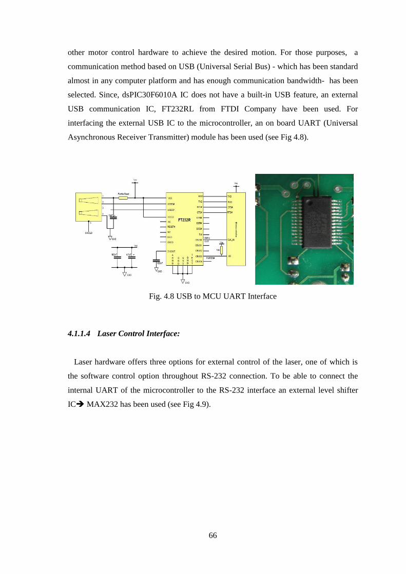
66
other motor control hardware to achieve the desired motion. For those purposes, a
communication method based on USB (Universal Serial Bus) - which has been standard
almost in any computer platform and has enough communication bandwidth- has been
selected. Since, dsPIC30F6010A IC does not have a built-in USB feature, an external
USB communication IC, FT232RL from FTDI Company have been used. For
interfacing the external USB IC to the microcontroller, an on board UART (Universal
Asynchronous Receiver Transmitter) module has been used (see Fig 4.8).
Fig. 4.8 USB to MCU UART Interface
4.1.1.4 Laser Control Interface:
Laser hardware offers three options for external control of the laser, one of which is
the software control option throughout RS-232 connection. To be able to connect the
internal UART of the microcontroller to the RS-232 interface an external level shifter
IC MAX232 has been used (see Fig 4.9).

67
Fig. 4.9 MCU to Laser Interface
For safety purposes, not all of the commands are available by software control (i.e.:
Global Enable). To produce those signals, external digital I/O pins on “PWM”
connector can be used.
4.1.1.5 Operational Status Tracking Elements:
For viewing the operational state of the board, there is also an on board
connector, which can be used for driving a either a 2 or 4 line character LCD (Liquid
Crystal Display). 3 on board LEDs can be adjusted to provide information about the
operational state of the PWM outputs. When the related motor control PWM output
have been configured as a standard digital I/O pin; they can also be used for any other
type of visual feedback (status tracking). Another led provides information about the
power input status of the board (see Fig 4.10).
Fig. 4.10 Status LEDs

68
4.1.1.6 External User Intervention:
User can externally modify the operation of the controller board, through the on board
push buttons that are observed in an event driven (interrupt based) manner by the
software. Buttons have been labeled as “+”, “-”, “F”, “B” to provide ease of use (see Fig
4.11).
Fig. 4.11 Push Buttons
4.1.1.7 Programming & Debugging Interface:
Controller board also have an ICSP(In Circuit Serial Programming) feature that
provides faster software development using an external programmer/debugger hardware
such as Pickit2 / ICD3. Below can be seen the example pin out for Pickit2.
Fig. 4.12 ICSP Connectivity and Programming
4.1.2 Design of DAC Board
Driver & controller platform for galvanometric scanners requires bi-polar, low noise,
clean, relatively large bandwidth control signals to precisely position the laser beam on

69
the work piece as desired. Selected 16bit LTC2642 DAC modules can provide low
0.5nV•sec glitch impulse and can support up to 50MHz SPI communication. Designed
PCB uses low noise split supply op-amps as output buffers to obtain the desired low
output impedance, bi-polar voltage output. Split supply bias voltage generation (i.e.
±5V) for DAC output drivers is done by an onboard capacitive charge pump IC
(MAX660). DAC module also has an on board precise voltage reference component so
that with the aid of voltage selection jumper, it is possible to switch between 4.096V
and 5V reference voltage options (see Fig 4.13).
Fig. 4.13 Schematic and Component View of DAC Module
4.2 Software
4.2.1 Embedded Software Design for Controller Board
After designing the controller board, next step was the selection of software
development environment that will be used in coding. Since C programming language -
compared to assemble language based tools - usually provides relatively faster code
development, CCS PICC C Compiler has been used as the embedded software
development platform for the dsPIC30F6010A. Compiler has also advantages like inline
asm code integration to C code for increased coding compatibility.
Code for the microcontroller platform has been implemented such that it’s working
algorithm is mainly based on interrupts; in other words done in an event driven fashion,
thus leading to a more conflict-free, time-efficient operation, especially considering the
various number of operations such as data acquisition, transferring of position data to

70
DACs through SPI bus; UART communication with PC and laser, external user
intervention and control.
The form for storing the machining data in controller environment has been chosen as
array based. Every single array contains “image” elements saved as struct data type.
Each “image” struct contains part of machining data that will later be sent to DACs and
laser in {X,Y,D} format such that 16-bit unsigned integer X, representing beam
position in X axis; 16-bit Y, representing position in Y axis; 8-bit D value either for
laser beam ON/OFF control (in B/W mode) or duty cycle value (in Grayscale Mode)
corresponding to power level adjustment parameter for software controlled high power
laser or small power visible test laser.
During the initial experiments; a standalone 5mWatt visible red laser, having the
wavelength of 640nm has been used, to test the reliability of DAC-Galvo operation and
proposed image formation approach, without excessively interacting with a 20Watt high
power laser, at least for the initial tryouts. The brightness level of used 5mW laser can
be adjusted using a TTL logic level 20kHz PWM signal. For that purpose high
resolution PWM features of the selected microcontroller have been used. The PWM
resolution (for edge-aligned mode) while controller operated at 120MHz clock
frequency can be found using:
𝑅𝑒𝑠𝑜𝑙𝑢𝑡𝑖𝑜𝑛 =log 2 •
fCY
fPWM
log 2
log 2•29,48 MHz
20kHz
log 2 = 11.5255 (where: fCY is the instruction clock)
It is around 11bit, which can be taken as acceptable for laser intensity adjustments.
4.2.2 GUI Design
Nowadays, most systems – whether an industrial solution or scientific research is the
main concern - have a built-in embedded intelligence that may require the transfer of
operational commands or data from a digital control platform (i.e.: industrial PC) to the
system, so an “intermediate step” software might be convenient in terms of both device

71
control, data transfer between digital platforms (i.e.: pc/laptop & controller board) also
making the system integration easier due to partial elimination of complex intermediate
hardware stages.
Considering most of today’s professional laser machining solutions, use user friendly
graphics based control environments so called GUIs (graphical user interface); a
windows form application based C# GUI has been implemented to meet similar
requirements.
Designed application simply gets an image file, than converts that file to a new image in
suitable format and size, and then extracts the pixel based image data and writes it to a
text file; content of which, later be transferred to the controller board and laser module
through serial (USB/RS-232) connections.
4.2.2.1 Design Method:
Chosen approach was using the .NET based C# software component available in
Microsoft Visual Studio. The program can export executable outputs with “.exe”
extension, removing the necessity for additional software installation; so that any
computer with appropriate RS-232 and USB can be used to operate the system. Other
advantages can be ordered as: communication through serial ports can be done easily in
an object based manner using the windows form application toolbox; many desired time
dependant features can be added to modify the operation of the system like counting
down, having time limited operation. Built-in toolboxes have visual elements that can
be used to view the levels of data acquisition signals, leading to nearly full status
tracking of the controller and interconnected hardware.
For ease of understanding the operation of GUI window, it can be evaluated in three
main parts in terms of functionality.
Part A:
That part includes controls for main actions and features related with image preparation:
- Importing source image to extract the target machining data

72
- Specifying width and height in pixels
- Scaling of the final machining data output
- Keeping aspect ratio might be enabled/disabled
- Choosing between Gray Scale & Black-White modes
- Exporting machining data to a text file
Part B:
That part includes controls for main actions and features related with device
configurations (laser, controller board), communication to realize machining data
transfer:
-Data transfer tracking windows for communication with laser through RS-232 and with
PC/Laptop through USB
-Manual control of digital I/O s where forced HW control is needed
-Laser Control Features:
HW Controlled (using digital I/O s):
Laser Disable, Laser Emission Gate Control
SW Controlled:
Laser Global Enable, Alignment Laser Disable/Enable, Laser Duty Factor, Laser Burst
Length, Laser Pulse Repetition Rate Selection, Laser Pulsed/CWM mode selection,
Laser Waveform Selection/Setting, Laser Power Adjustment, Task Start, and Turn
ON/OFF
Part C :
That part includes controls for main actions and features related with galvo output
control and output machining data:
-Galvanometric scanner enable/disable

73
-Selecting the output data to be machined (extracted from a file or stored in the
memory)
4.2.2.2 Operation of the GUI:
Part A - To obtain the machining data from an image, imported source image file
should have one of the “.jpg” “.jpeg” “.bmp” “.gif” file extensions. Once successfully
imported the image file can be viewed from the picture box. Then in the next step user
should decide width and height parameters in pixels for the machining data output that
will be extracted from the source image. Calculated pixel count of the new image is
shown in pixels tab. One should note that ordinary image resizing operations can lead to
distortion in image quality so that in our case the technique that has been used for image
conversion is interpolation based so resizing causes less image distortion. While
resizing, it is user’s choice whether to keep the aspect ratio between width and height of
the image or to resize it with a new desired ratio. Other parameter to be adjusted is the
final scaling factor value that can be used to make ordinary scaling of the output image
so that it can directly be used by the controller to drive the DACs, hence also the galvos
for more or full utilization of the galvo’s scanning range. As previously stated each
machining data output contains x,y coordinates for the related pixel and a light intensity
value. The method for obtaining the intensity value is based on reading the RGB values
of a certain pixel each represented with a byte. Since this machining application and
reference images has a monochromatic nature, it has only been focused on the G value
(R or B also can be used since they all give same result in existing case) and that has
been compared with 128; such that values higher than 128 produces “1” corresponding
to “ON” state of the laser and values smaller than 128 produces “0” which means laser
beam “OFF”. If gray-scale mode is active then this comparison is not made and G
value is directly sent to be later used for intensity information of the laser beam.
Part B - In the device communication and control part of the GUI: after
activating the desired devices and choosing the COM ports related with each device
(controller board, laser) and desired communication Baud rates; in the next step,
parameters such as laser burst length, laser pulse repetition rate, laser output power
(controlled based on stby and active state current levels), laser duty factor and laser

74
waveform can be adjusted by entering numeric inputs. Other features related with laser
operational modes and controlled by checkboxes can be ordered as: Pulsed/CWM mode
selection and alignment laser ON/OFF control. Remaining functions such as task start,
shutdown can be implemented by using buttons.
Part C - Machining data can either be based on data obtained from an imported
image or available patterns such as dots, lines, circle, varying sine wave figures stored
in controller board’s program memory. The source for that data can be specified by
using the data source selection menu. After enabling the galvos from the GUI control
panel, selected data can be diverted to drive to the DACs on the controller board to
actuate the galvos and form the target pattern on the work piece.
Fig. 4.14 GUI on a sample run
4.3 Mechanical Design
The experimental studies require the accurate positioning of the optics, as well
as their proper connection with the electromechanic systems. For such purposes,
additional mechanical parts have been designed in Solid Works environment, machined
and used during the experimental studies. That part tries to cover the design procedure
of the mechanic parts and working principles.

75
4.3.1 Fine Focusing Mechanism
Most of the distances-lengths corresponding to optical parameters have been
decided by the telecentric scanning lens design specifications so that correct placement
of the scanning lens becomes crucial. Due to the system tolerances related with the
mechanical parts, and their positioning relative to each other, fine adjustment of the
telecentric scanning lens for proper focusing is essential. So under the guidelines of
these requirements, a fine focusing mechanism has been developed (see Fig 4.15).
Fig. 4.15 LSM02 Technical Drawing
Operational principle of the designed manual focusing mechanism can be
summarized as: the rotational motion results a lens movement along the focusing axis
(e.g. CW rotation moves the lens “up” away from the work piece; whereas CCW
rotation moves the lens “down”towards the work piece. As can be understood from
the figure above, the pitch size for the lens threads is 0.75mm. Considering the pitch
size and number of threads (which is 5 for the LSM02 lens); using the lens threads
directly might have degrade the mounting stiffness after a few turns in CCW rotation;
so an outer ring with a single-start thread structure and finer pitch value has been
designed and machined to be able to reach higher focusing adjustment resolution.

76
The inner side of the designed ring has female thread directly matching to the
lens (again 0.75mm); but the outer side of the ring has a male thread with a finer pitch
of 0.5 mm and lower thread angle, thus together leading to more precise adjustment of
the lens position through the focusing axis. One other advantage of the ring mechanism
is that, due to the higher total threaded length (9.96 mm), the ring makes it possible to
go at a closer distance towards Y-axis mirror. That value is higher compared to the case
in which overall focusing action is limited with the vertical distance of 0.75mm*5 turns
approximately 3.75mm total threaded length of the lens itself.
Finally that ring sits in a counterpart having a female thread and 0.5mm pitch.
The counter part is tight-fixed to a rectangular plate that is mounted on the galvo
assembly. CAD drawing and photo of the produced part mounted on the galvo assembly
is given in the following figure 4.16 (“blue” shows the ring and “green” shows the
plate):
Fig. 4.16 Focusing Mechanism
Note: Incoming beam is shown by RED; reflecting beam shown by GREEN; outgoing
beam shown by CYAN

77
4.3.2 Beam Expander Mounting Part
Laser beam transferred with the fiber optical guide finally comes out through a
beam expander unit so that the outcoming beam can be focused more effectively by the
final focusing mechanism. Laser beam expander unit should be fixed firmly to the galvo
assembly to be able to properly feed the incoming laser beam to the X-axis mirror.
Mentioned beam expander unit is shown in the figure 4.17 below:
Fig. 4.17 Beam Expander
Considering the size and geometry of the expander unit (see Appendix E) and
also taking into account that the centre of the laser beam should be coincident with the
center of the target X-axis mirror; an appropriate part, satisfying these demands, has
been designed and produced. CAD drawing and photo of the machined part is given in
the following figure 4.18:
Fig. 4.18 Beam Expander Mount

78
For safety issues and to prevent damage to surrounding environment another
requirement is that the regions where active laser radiation exists should be in an
isolated closed form as much as possible; but due to the design geometry of the galvo
assembly a fully-closed enclosure does not seem to be feasible. So those parts also form
a semi-closed enclosure that minimizes the laser radiation to emit out of the allowable
region.
4.3.3 Mirror Inertia Calculations (for simulations)
In this part inertias of the mirrors have been calculated using software tools, to
use that information later in the simulation model of the galvo models. During the
simulations, the inertia values have been applied to the system as disturbance terms to
improve the reliability of the simulation model.
This procedure can be summarized as: creating the mirrors in Solid Works
design environment and calculating the inertias of the mirrors using the built-in inertia
calculation tool of the Solid Works. Below shown the 3D drawings of the mirrors in
Solid Works:
Fig. 4.19 X-axis mirror Fig. 4.20 Y-axis mirror
The inertia values obtained using the tools are like the following:

79
Fig. 4.21 Calculated Inertia Values
Considering the coordinate plane specified in the figures, one should note that rotary
action is along “Y” axis for “X-mirror” and along “X” axis for “Y-mirror”. The inertia
values related with rotation is marked with red dots: Ix=24.77 gr ∗ mm2=24.77 x 10⁻⁹
𝑘g ∗ m2 & Iy=20.58 gr ∗ mm2=20.58 x 10⁻⁹ 𝑘g ∗ m2

80
5 EXPERIMENTS & CONCLUSION
5.1 Experiments
Experimental studies of the thesis work can be handled in two main parts:
- Macro level image formation experiments
- Micro level machining experiments
A) Macro level image formation experiments using a visible spectrum laser:
During that part of experiments the main aim has been the proof of image projection
concept to ensure the reliable operation of galvanometric scanner system hardware as
well as control software.
Equipments: (in addition to default scanning hardware and electronics)
- Laser Pointer
Fig 5.1 Laser Pointer
- PDQ80A PSD (Position Sensing Detector)

81
Fig 5.2 PSD Device
Laser Pointer:
It is a visible spectrum 5mWatt laser with 640nm wavelength and a modulation input
that can be driven using a TTL level 20kHz modulation signal so that beam intensity
control can be done. The focusing has been adjusted by using the built in collimator of
the laser.
PDQ80A PSD:
A PSD device from Thor Labs Company having a segmented-quadrant (see Appendix
F) device structure and separate analog voltage outputs for each axis.
Method:
Image data to be projected on the surface, have been stored in program memory of the
designed supervisory board. Analog drive signals for the galvo servo driver boards have
been produced by using the designed DAC board which has been controlled according
to the image data coming from the supervisory board through 20MHz SPI
communication interface. Galvos have been used to steer the laser beam on the target
surface. No additional focusing mechanism has been used.
Continuous line images: (laser continuously ON)
Using that method phase and frequency varying sine wave variation curves (Lissajous
Curves) have been formed. See following figures.

82
Fig. 5.3 Snapshots from a rotating Lissajous Curves
Another stage in experiments can be thought as “intermediate” transition
between macro and micro level experiments. Above stated PDQ80A PSD device has
been used to test the micro level scanning operation and closed loop data acquisition
capability (i.e. 16-bit external ADC) of the supervisory board (especially for possible
future closed loop power tracking). To eliminate the noise in obtained signals, 10 Hz
low pass filter has been considered as a remedy but that causes the side affect of
decreasing bandwith so for high speed scanning tests that method has been left aside
and rest of the experiments have been established by high power laser module and
machining on materials.
Fig. 5.4 PSD output for micro scale curve
Discontinuous line images (with laser ON/OFF modulation):
In that type of image creation the laser is ON between any two consecutive points where
the smallest unit curve (i.e. line) exists; and OFF during a blank transition. Using this
method vector images such as geometric shapes, logos have been formed (see Fig. 5.5).

83
Fig. 5.5 Laser Radiation Logo
B) Micro level machining experiments with high power laser
During that part of experiments the main aim has been the laser micro scribing of a
projected image on a target surface by using before mentioned direct-write method and
raster scanning approach.
Equipments: (in addition to default scanning hardware and electronics)
- LSM02-BB telecentric scanning lens
- 20Watt 1064nm pulsed-fiber laser module
- 7.0X Beam Expander
Method:
Image data to be scribed on the surface, have been extracted using the designed GUI
and transferred to the program memory of the designed supervisory board through USB
interface. Analog drive signals for the galvo servo driver boards have again been
produced by using the designed DAC board which has been controlled according to the
image data coming from the supervisory board through serial communication interface.
Galvos have been used to divert the laser beam on the lens surface and the focusing of
the beam has been implemented by using the specified lens. Following figure 5.6 shows
general view of experimental setup.

84
Fig. 5.6 Experimental Setup
Various scanning rates and output powers have been used. Materials such as special
laser alignment paper, brass disc, and optical storage discs have been evaluated during
the experiments. Scribed surfaces have been viewed using an optical microscope.
In the experiments additional variable scaling factors have been used which makes
location of each spot has been decided by the “pixel coordinate x scaling factor”, plus
an additional centralizing offset value of 32768, that has been used to form an image
normalized to the center of coordinate plane. There is also an internal multiplier which
is set experimentally so that between each adjacent pixels the digital value send to
DACs have been incremented by “internal multiplier x scaling factor” (over 655536).
Since machining performance relies on fundamental parameters like spot size, initial
experiments have been concentrated on focusing. Following are the results obtained for
different materials and power levels:
*Material: Bristol cartoon covered with cellophane coating, Thickness= 0.33 mm
approximately.

85
Fig. 5.7 Bristol Cartoon Hole
Note: Each gap is 0.5mm
Average Power Level: 4 Watt approximately (linear power output assumption for ease
of calculation) Pulse Rate: 25kHz, Burst Length: 2seconds
Comment: The region that photo thermal effect occurs is larger compared to drilled hole
itself.
*Material: Black ABS plastic, thickness 2 mm approximately
Fig. 5.8 ABS Plastic
Average Power Level: 8 Watt approximately (linear power output assumption for ease
of calculation) Pulse Rate: 25kHz Burst Length: 1seconds.
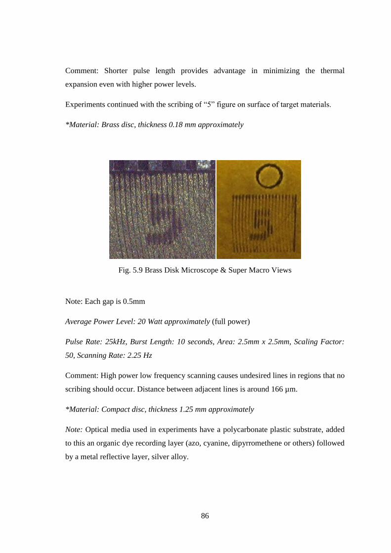
86
Comment: Shorter pulse length provides advantage in minimizing the thermal
expansion even with higher power levels.
Experiments continued with the scribing of “5” figure on surface of target materials.
*Material: Brass disc, thickness 0.18 mm approximately
Fig. 5.9 Brass Disk Microscope & Super Macro Views
Note: Each gap is 0.5mm
Average Power Level: 20 Watt approximately (full power)
Pulse Rate: 25kHz, Burst Length: 10 seconds, Area: 2.5mm x 2.5mm, Scaling Factor:
50, Scanning Rate: 2.25 Hz
Comment: High power low frequency scanning causes undesired lines in regions that no
scribing should occur. Distance between adjacent lines is around 166 µm.
*Material: Compact disc, thickness 1.25 mm approximately
Note: Optical media used in experiments have a polycarbonate plastic substrate, added
to this an organic dye recording layer (azo, cyanine, dipyrromethene or others) followed
by a metal reflective layer, silver alloy.

87
Fig. 5.10 CD
Average Power Level: 3 Watt approximately (linear power output assumption for ease
of calculation), Pulse Rate: 50kHz, Burst Length: 2 seconds, Area: 3mm x 3mm, Scaling
Factor: 50, Scanning Rate: 2.25 Hz
Comments: Undesired pixels circled are due to rounding-up of pixel intensity data and
related with imaging data itself not a marking error. The lines parallel to horizontal axis
(circled with green) occur because of turning back to initial scanning start point at the
end of each full scanning of the image data array. So for the following experiments bi-
directional scanning technique has been used.
*Material: Compact disc, thickness 1.25 mm approximately
Fig. 5.11 20x20 “5” on CD

88
Average Power Level: 2 Watt approximately (linear power output assumption for ease
of calculation) Pulse Rate: 50kHz, Burst Length: 2 seconds, Area: <1mm x 1mm (20 x
20 pixels), Scanning Rate: 2.25 Hz
*Material: DVD+R disc, thickness 1.25 mm approximately
Fig. 5.12 32x32 “5” on DVD
Average Power Level: 2 Watt approximately (linear power output assumption for ease
of calculation) Pulse Rate: 25kHz, Burst Length: 2 seconds, Area: 1mm x 1mm (32 x 32
pixels), Scaling Factor: 10, Scanning Rate: 0.86Hz
Comments: Inverted version of the extracted image data has been used so that “black
pixels” on the reference image means laser ON while “white pixels” corresponds to
laser OFF condition. Number of undesired pixels decreased clearly, leading to a finer
marking. The distance between center of spots can be calculated as less than 1000 µm /
32= 31.25 µm (technical spec given for LSM02-BB points to a 13 µm minimum
achievable spot size); because the gap between adjacent spots can still be distinguished
in horizontal axis. Although the reference image resolution is the same for both vertical
89
and horizontal axis; marks along vertical axis are in a more “continuous” fashion
compared to the general behaviour along horizontal axis. This effect might be occurring
due to the horizontal scanning at low speeds, such that the fast scanning in vertical axis
- this is actually what forms the equivalent “vertical scanning line effect”- results with
many consecutive laser spots affecting short time after each other extracting more heat
and leaving less time for cooling down thus leading to combining of transition regions
between spots.
Internal multiplier has been selected as “18” experimentally, so that the digital value
send to DACs have been incremented at least by 180 (10 x 18); which means galvo
modules can still be forced for increasing resolution (of course considering the ±1LSB
INL and DNL changes over temperature of the DACs).
5.2 Conclusion
The design and implementation of a laser micromachining system, mainly targeting
micro scribing and marking operations have been explained in previous several
chapters, together with the theoretical background and proof of overall system
functionality. Following is the summary of the conclusions of this research work.
1) Laser micromachining parametric relations:
Before laser machining, parameters related to the material removal rate should be
examined. Machining of different materials may require examination of different
machining parameters, including laser intensity, number of laser pulses, scanning rate. It
is obvious that a higher energy level and higher number of laser pulses provide a higher
material removal rate. Higher scanning rates cause less thermal deformation in the
regions where no machining should occur.
2) Scanning Techniques:
Raster scanning approach requires the use of bi-directional back and forth steering of
the laser beam to maximize useful bandwidth of the galvo modules and minimizing
undesired markings due to fast transitions between adjacent columns or rows.
Bandwidth increase is due to small angle bandwidth being larger than large angle
bandwidth so avoiding long trajectories provide such an advantage.

90
3) Machining Resolution
In machining operations, the focused spot size that can be achieved with fast pulsed
operation is smaller than it’s with slow continuous wave mode operation. Decreasing
pulse repetition may contribute in similar way. These effects are mainly due to lack of
thermal deformation in pulsed case.
4) Scanning Approach - Operational Performance Relation
Raster scanning approach usually provides better results in marking operations whereas
vector scanning may be more convenient for drilling, cutting type of applications.
5) Modification of machining area requires the consideration of power level
To obtain better linearity in terms of optical power control, an external closed loop
control system based on optical sensors can provide advantage in gray scale marking
and scribing.
6) Machining Control Algorithm
A control algorithm that includes scanning speed rate adjustment feature or auto power
tuning depending on machining area is necessary for reliable operation.
91
6 POSSIBLE FUTURE WORK
So far, the content and results of this research work have been summarized. It
mainly focuses on laser micromachining by implementation of fast marking operations
on certain type of materials. Behind this research, there are several possibilities for
future work
1) Increasing the scanning resolution:
Staying within the limits of existing hardware, the image resolution might be increased
further.
2) Extending machining area:
Machining to a larger area without sacrificing from the resolution might be possible
with the synchronization of scanning elements and additional motion stages to move the
work piece.
3) Parametric study of machining and measurement:
Forming tables to be able to observe the relation between machining parameters,
material types and type of processing job might contribute to the performance and
effectiveness of overall processing procedure. SEM (Scanning Electron Microscopy)
technique can be used for more detailed measurements.
4) Improvement of machining quality and extending range of target materials:
The laser that has been used during this study is a nano-second pulse type. However, it
may be difficult to produce high quality machining surfaces on most materials due to
photo thermal heat effect being dominant in nano-second machining. A possible
improvement might be promoting to a femto or picosecond pulse time laser.

92
5) Improving vector scanning compatibility:
For now, designed system can also be used for vector scanning purposes; but this
capability is limited with the use of third party programs to obtain the necessary vector
scanning information. In that context, vector data extraction feature might be integrated
to the control software so that it can provide convenience in drilling, cutting type of
applications.
6) Adding external data storage feature:
To increase the standalone behavior of the system (for example: fully eliminating the
dependency on a controller PC), an external storage feature might be added by
interfacing with a SD (Secure Digital) card through SPI communication.
7) Closed loop optical power tracking:
With the use of additional optics - such as beam splitter mechanism - tracking of beam
power level can be implemented so that closed-loop optical power control can be
realized.

93
REFERENCES
[1] Madou, M.J., “Fundamentals of microfabrication: the science of miniaturization
(2nd ed)”, CRC Press LLC, 2002.
[2] Xia, Y., Whitesides, G.M., “Soft lithography”, Annu. Rev. Mater. Sci., 28, 1998, pp.
153-184.
[3] Park, J.W., S.S. Lee, B.S. So, Y.H. Jung, N.Kawasegi, N.Morit and D.W. Lee,
“Characteristics of mask layer on (100) silicon induced by tribo-nanolithogrphy with
diamond tip cantilevers based on AFM”, Journal of Materials Processing Technology,
Vol. 187-188, 2007, pp. 321-325.
[4] Stiévenard, D., and B. Legrand, “Silicon surface nano-oxidation using scanning
probe microscopy”, Progress in Surface Science, Vol. 81, 2006, pp. 112-140.
[5] Vieu, C., Carcenac, F., Pépin, A., Chen, Y., Mejias, M., Lebib, A., Manin- Ferlazzo,
L., Couraud, L., and Launois, H., “Electron beam lithography: resolution limits and
applications”, Applied surface science, 164, 2000, pp. 111-117.
[6] Crafer, R.C., Oakley, P.J. (Eds.), Laser Processing in Manufacturing, Chapman &
Hall, London (1993).
[7] Riccardi, G., M. Cantello, F. Mariotti, P. Giacosa, Micromachining with excimer
laser, Ann. CIRP 47 (1) (1998) 145–148.
[8] Gower, M.C., “Industrial applications of laser micromachining”, Optics express,
7(2), 2000, pp. 56-67.
[9] Ogura, G., Angell, J., Wall, D., Applications test potential of laser micromachining,
Laser Focus World 34 (1998) 117–123.
[10] Klimentov, S.M., Garnov, S.V., Kononenko, T.V., Konov, V.I., Pivovarov, P.A.,
Dausinger, F., High rate deep channel ablative formation by picosecond–nanosecond
combined laser pulses, Appl. Phys. A 69 (1999) 633–636.
[11] Hoving, W., Laser fine adjustment, in: Proceedings of the ICALEO, 2001.
[12] Windholz, R., P. Molian, Nanosecond pulsed excimer laser machining of CVD
diamond and HOPG graphite, J. Mater. Sci. 32 (1997) 4295–4301.
94
[13] Spur, G., Industrial cleaning technologies for hard surfaces: dry ice blasting and
laser, in: Proceedings of the 40th International detergency Conference IDC’01, 2001,
pp. 156–165.
[14] Ishizaka, Y., Watanabe, K., Fukumoto, I., Ohmura, E., Miyamoto, I., Three-
dimensional molecular dynamics simulation on laser materials processing of silicon, in:
Proceedings of the ICALEO98, 1998, pp. A55–A63.
[15] Basting D., Marowsky, G., “Excimer laser technology”, Springer-Verlag Berlin
Heidelberg, 2005.
[16] Meijer, J., Du, K., Gillner, A., Hoffmann, D., Kovalenko, V.S., Matsunawa, T.,
Ostendorf, A., Poprawe, R., Schulz, W., Laser machining by short and ultra short
pulses, state of the art and new opportunities in the age of the photons, Ann. CIRP 51
(2) (2002) 531–550.
[17] Paterson, C., Holmes, A.S., and Smith, R.W., “Excimer laser ablation of
microstructures: A numerical model”, Journal of applied physics, 86(11), 1999, pp.
6538-6546.
[18] Saxena, I., Agrawal, A., and Joshi, S.S., “Fabrication of microfilters using excimer
laser micromachining and testing of pressure drop”, J.Micromech. Microeng, 19, 2009,
pp. 025025-1-025025-10.
[19] Basting, D., Excimer Laser Technology: Laser Sources, Optics, Systems and
Applications, Lambda Physik AG, Göttingen (D), 2001.
[20] Chen, X., Liu, X., Short pulsed laser machining: how short is short enough? J.
Laser Appl. 11 (6) (1999) 268–272.
[21] Bosman, J., Laser engraving processes, Ph.D. Thesis, University of Twente, in
preparation.
[22] Zheng, H.Y., Liu, H., Wan, S., Lim, G.C., Nikumb, S., and Chen, Q., “Ultra short
pulse laser micromachined microchannels and their application in an optical switch”,
Int. J. Adv. Manuf. Technol., 27, 2006, pp. 925-929.
[23] Dubreucq, G.M., Zahorsky, D., KrF excimer laser as a future deep UV source for
projection printing, in: Proceedings of the InternationalConference on Microcircuits
Engineering, 1982, pp. 73– 78.
[24] Rowan, C., Excimer lasers drill precise holes with higher yields, Laser Focus
World August (1995).

95
[25] Ben, A. -Yakar et al., “Femtosecond laser machining of fluidic microchannels for
miniaturized bioanalytical systems,” Proceedings of SPIE, Vol. 4637, p. 212-217
[26] Harvey, E.C., Rumsby, P.T., Fabrication techniques and their application to
produce novel micromachined structures and devices using excimer laser projection, in:
Proceedings of the SPIE Conference on Micromachining and Microfabrication Process
Technology III, Vol. 3223, 1997, pp. 26–33.
[27] Rizvi, N.H., Harvey, E.C., Rumsby, P.T., Burt, J.P.H., Talary, M.S., Tame, J.A.,
Pethig, R., An excimer laser micromachining system for the production of bioparticle
electromanipulation devices, in: Proceedings of the SPIE Conference on
Micromachined Devices and Components III, Vol. 3224, 1997, pp. 266–272.
[28] Meijer, J., in: J.A. McGeough (Ed.), Micromachining Materials, Marcel Dekker,
2002, pp. 203–237.
[29] Xie J., Huang S., Duan Z., Shi Y.,Wen S., Correction of the image distortion for
laser galvanometric scanning system. Opt Laser Technol 2005; 37: 305–11.
[30] Chen M.F., Chen Y.P., Compensating technique of field-distorting error for the
CO2 laser galvanometric scanning drilling machines. IntJ Mach Tools Manuf 2007; 47:
1114–24.
[31] Fischer R.E., Tadic-Galeb B., Optical system design. New York: McGraw-Hill;
2000.
[32] Asif Sabanovic and Kouhei Ohnishi, Motion Control Systems, Wiley, Singapore,
2011, ISBN 978-0-470-82573-0.

96
APPENDICES
Appendix A
Definitions of Scan Lens Parameters & Specs
Scanning Distance (SD): The SD is the distance between the galvo mirror pivot
point and the back mounting plate of the objective. Since the LSM scan lens is
telecentric, the galvo mirror pivot point must be located at the back focal plane
of the objective in order to maximize image resolution.
Pupil Size (EP): The size of the EP determines the ideal 1/e2 collimated beam
diameter that should be used for the beam of light used to image the sample in
order to maximize the resolution of the imaging system. Used scan lenses have
an EP 4 mm in diameter.
Working Distance (WD or LWD): The distance between the tip of the scan
lens housing and the front focal plane of the scan lens is defined as the WD.
Depth of View (DOV): The DOV parameter reported for the scan lenses
corresponds to the distance between the front focal plane and a parallel plane
where the beam spot size has increased by a factor of the √2.
Field of View (FOV): The FOV is the maximum size of the area on the sample
that can be imaged with a resolution equal to or better than the stated resolution
of the LSM scan lenses. In order to meet this specification the imaging system
must be designed to properly utilize the LSM scan lenses in the system.
Parafocal Distance (PD): The PD is the distance from the scan lens mounting
plane to the front focal plane of the scan lens.
Curvature (C): The curvature is the maximum distance between the front focal
surface and an ideal plane.

97
Scan Angle (SA): The SA is the maximum allowed angle (in the X or Y
direction) between the beam and the optical axis of a scan lens after being
reflected off of the galvo mirror
LSM Series Lens Specs Chart
Appendix B
Reasons of Image Distortion
The deflection of a laser beam with a two-mirror system results in three effects:
(1) The arrangement of the mirrors leads to a certain distortion of the image field –see
Fig. B.1 below.

98
Fig. B.1 Field Distortion in a Two-way Mirror Deflection System
This distortion arises from the fact that the distance between mirror 1 and the image
field depends on the size of the scan angles of mirror 1 and mirror 2. A larger scan angle
leads to a longer distance.
(2) The distance in the image field is not proportional to the scan angle itself, but to the
tangent of the scan angle. Therefore, the marking speed of the laser focus in the image
field is not proportional to the angular velocity of the corresponding scanner.
(3) If an ordinary lens is used for focusing the laser beam, the focus lies on a sphere. In
a flat image field, a varying spot size is the result.
As a result, the scanning field turn out to be a "pillow-shaped" image, see Fig. B.2
below.

99
Fig. B.2 Pillow-shaped Field Distortion Caused by the Arrangement of Mirrors
The F-Theta objective, however, causes a barrel-shaped distortion of the image field.
See Fig.B.3
Fig. B.3 Types of Field Distortion a) Pillow Shaped b) Barrel-Shaped c) Barrel- Pillow
Shaped
Appendix C
Reflection Curve for Silver Coated Mirrors

100

101
Appendix D
Laser Control
Status Word Bit Values
(*)Changes of these bits require the Task Status Enable bit (STATUS word bit 1) to be
asserted to affect the change.
(**)This bit is stored in non-volatile memory and is remembered by the laser after
turning the laser power off

102
RS-232 Command Set

103

104
Appendix E
Mechanical Parts
E.1 Beam Expander Technical Specs
E.2 Beam Expander Technical Drawing

105
E.3 Focusing Adjustment Mechanism
Ring
Plate

106
E.4 Beam Expander Mount

107
Appendix F
Segmented-Quadrant Sensing Detectors
F.1 Segmented-Quadrant Detectors
F.2 PDQ80A Specs

108
Appendix G
Links
Coherent. Understanding Laser Beam Parameters. Retrieved July 2011, from
http://www.coherent.com/downloads/UnderstandingLaserBeamParameters.pdf
Coherent. Best Practices White Paper. Retrieved July 2011, from
http://www.coherent.com/Downloads/Best_Practices_Whitepaper.pdf
FTDI Company. FT232R USB UART IC Datasheet Version 2.09. Retrieved December 2010, from http://www.ftdichip.com/Support/Documents/DataSheets/ICs/DS_FT232R.pdf
Linear Technologies. LTC1859 8-Channel, 12-/14-/16-Bit,100ksps SoftSpan A/D Converters with
Shutdown. Retrieved November 2010, from http://cds.linear.com/docs/Datasheet/185789fa.pdf
Linear Technologies. LTC2641/LTC2642 16-/14-/12-Bit VOUT DACs in 3mm × 3mm DFN. Retrieved
November 2010, from http://cds.linear.com/docs/Datasheet/26412fb.pdf Maxim. CMOS Monolithic Voltage Converter. Retrieved March 2011, from http://datasheets.maxim-
ic.com/en/ds/MAX660.pdf
Microchip. DsPIC30F6010A/6015 Data Sheet High-Performance, 16-bit Digital Signal Controllers.
Retrieved March 2011, from http://ww1.microchip.com/downloads/en/DeviceDoc/70150E.pdf
Microchip. Dspic Reference Manual Serial Peripheral Interface (SPI). Retrieved April 2011, from
http://ww1.microchip.com/downloads/en/DeviceDoc/70067E.pdf
Microchip. PICkit. 2 Programmer/Debugger Use’s Guide. Retrieved March 2011, from http://ww1.microchip.com/downloads/en/DeviceDoc/51553E.pdf
SPI Laser. redENERGY G3 Made for. Retrieved June 2011, from
http://www.spilasers.com/Products/redENERGY_G3.aspx? Texas Instruments. MAX232, MAX232I EIA Line Drivers/Receivers. Retrieved April 2011, from http://focus.ti.com/lit/ds/symlink/max232.pdf
Thorlabs, Inc. - Your Source for Fiber Optics, Laser Diodes, Optical Instrumentation and Polarization.
Retrieved June 2011, from http://www.thorlabs.de/index.cfm?
USB. Universal Serial Bus. Retrieved May 2011, from http://www.usb.org/home