design guidelines for the implementation of...
TRANSCRIPT

DESIGN GUIDELINES FOR THE IMPLEMENTATION
OF EMBEDDED NETWORK ON CHIP (NOC) IN FPGAS
By
Noha Gamal Mohamed
A Thesis Submitted to the
Faculty of Engineering at Cairo University
in Partial Fulfillment of the
Requirements for the Degree of
MASTER OF SCIENCE
in
Electronics and Communications Engineering
FACULTY OF ENGINEERING, CAIRO UNIVERSITY
GIZA, EGYPT
2017

DESIGN GUIDELINES FOR THE IMPLEMENTATION
OF EMBEDDED NETWORK ON CHIP (NOC) IN FPGAS
By
Noha Gamal Mohamed
A Thesis Submitted to the
Faculty of Engineering at Cairo University
in Partial Fulfillment of the
Requirements for the Degree of
MASTER OF SCIENCE
in
Electronics and Communications Engineering
Under the Supervision of
Prof. Dr. Hossam A. H. Fahmy
Dr. Hassan Mostafa
Professor
Electronics and Communications
Engineering Department
Faculty of Engineering, Cairo University
Assistant Professor
Electronics and Communications
Engineering Department
Faculty of Engineering, Cairo University
FACULTY OF ENGINEERING, CAIRO UNIVERSITY
GIZA, EGYPT
2017

DESIGN GUIDELINES FOR THE IMPLEMENTATION
OF EMBEDDED NETWORK ON CHIP (NOC) IN FPGAS
By
Noha Gamal Mohamed
A Thesis Submitted to the
Faculty of Engineering at Cairo University
in Partial Fulfillment of the
Requirements for the Degree of
MASTER OF SCIENCE
in
Electronics and Communications Engineering
Approved by the
Examining Committee
____________________________
Prof. Dr. Hossam A. H. Fahmy, Thesis Main Advisor
____________________________
Prof. Dr. Amin Nassar, Internal Examiner
____________________________
Prof. Dr. Mohab Anis, External Examiner (Electronics and Communications Engineering, The American University in Cairo)
FACULTY OF ENGINEERING, CAIRO UNIVERSITY
GIZA, EGYPT
2017

Engineer’s Name: Noha Gamal Mohamed
Date of Birth: 21/01/1987
Nationality: Egyptian
E-mail: [email protected]
Phone: +20 1003826997
Address: Electronics and Communications
Engineering Department,
Cairo University, Giza 12613, Egypt
Registration Date: 10/11/2011
Awarding Date: --/--/2017
Degree: Master of Science
Department: Electronics and Communication Engineering
Supervisors:
Prof. Dr. Hossam A. H. Fahmy
Dr. Hassan Mostafa
Examiners:
Prof. Dr. Hossam A. H. Fahmy (Thesis main advisor)
Prof. Dr. Amin Nassar (Internal examiner)
Porf. Dr. Mohab Anis (External examiner)
(Electronics and Communications Engineering, The
American University in Cairo)
Title of Thesis:
Design Guidelines for the Implementation of Embedded Network on Chip (NoC) for
FPGAs
Key Words:
Network on Chip; Fields Programmable Gate Array
Summary:
In this thesis, a literature survey of existing Networks-on-Chips is presented, then a
comparative review between the NoCs with available source code from area and speed
respective is provided. Efficiency gaps between hard and soft implementations using
FPGA-embedded NoC have been analyzed and designs recommendations have been
proposed. Finally two soft implantations are introduced to attempt the maximum
reduction of either the delay gap or the power gap between soft and hard
implementations.

i
Acknowledgments
First of all, I would like to thank Prof. Hossam Fahmy and Dr. Hassan Mostafa for
giving me the opportunity to work onto this subject which interests me a lot and
enhances my knowledge and career. I would also like to thank Dr. Hassan for his help,
suggestions and support.

ii
Table of Contents
ACKNOWLEDGMENTS .............................................................................................. I
TABLE OF CONTENTS .............................................................................................. II
LIST OF TABLES ......................................................................................................... V
LIST OF FIGURES ..................................................................................................... VI
NOMENCLATURE ................................................................................................... VII
ABSTRACT .............................................................................................................. VIII
CHAPTER 1 : INTRODUCTION ................................................................................ 1
1.1. MOTIVATION ........................................................................................ 1
1.2. CONTRIBUTION .................................................................................... 2
1.3. ORGANIZATION OF THE THESIS ............................................................ 2
CHAPTER 2 : LITERATURE SURVEY OF EXISTING NETWORKS-ON-
CHIPS .............................................................................................................................. 3
2.1. INTRODUCTION .................................................................................... 3
2.2. FPGA VERSUS ASIC ........................................................................... 3
2.2.1. Unit Costs ............................................................... 3
2.2.2. Non Recurring Engineering Costs........................................................... 4
2.2.3. Time to Market ............................................................... 4
2.2.4. System Re-Usability ............................................................... 5
2.2.5. Design Cycle ............................................................... 5
2.2.6. ASIC versus FPGA Summary ............................................................... 6
2.3. NOCS OVERVIEW ................................................................................. 6
2.3.1. Switching ............................................................... 8
2.3.2. Flow Control ............................................................... 8
2.3.3. Virtual Channel ............................................................... 9
2.3.4. Allocator .......................................................... 9
2.3.5. Implementation ............................................................... 9
2.4. PREVIOUS WORKS ................................................................................ 9
2.4.1. NoCem .......................................................... 9
2.4.2. PNoC ........................................................ 10
2.4.3. Dual Crossbar Router ............................................................. 12
2.4.4. HW NoC ........................................................ 14
2.4.5. SOTA ........................................................ 15
2.4.6. CONNECT ............................................................. 16
2.4.7. Split and Merge PS ............................................................. 18
2.4.8. FLNR ........................................................ 20
2.4.9. RROCN ........................................................ 23
2.5. COMPARATIVE REVIEW BETWEEN NOCS WITH OPEN-SOURCE CODE 25
2.5.1. Comparison Work Flow ............................................................. 25 2.5.1.1. Frequency ................................................................................................................. 25
iii
2.5.1.2. LUTs Usage ............................................................................................................. 27 2.5.1.3. Registers Usage ........................................................................................................ 29
2.6. SUMMARY AND FUTURE WORKS ....................................................... 30
CHAPTER 3 : SOFT AND HARD IMPLEMENTATIONS FOR FPGA-
EMBEDDED NOC ....................................................................................................... 33
3.1. INTRODUCTION .................................................................................. 33
3.2. METHODOLOGY ................................................................................. 33
3.2.1. Soft Implementation Flow ............................................................. 33
3.2.2. Hard Implementation Flow ............................................................. 34
3.3. RESULTS AND DISCUSSIONS ............................................................... 34
3.3.1. Input Module ............................................................. 35
3.3.2. Output Module ............................................................. 35
3.3.3. Routing Module ............................................................. 38
3.3.4. Allocator ........................................................ 38
3.3.5. Switch ........................................................ 38
3.3.6. Module and System levels comparisons ............................................... 38
3.4. DESIGN RECOMMENDATION ............................................................... 39
3.5. SUMMARY .......................................................................................... 40
CHAPTER 4 : TWO SOFT IMPLEMENTATIONS FOR FPGA-EMBEDDED
NOC ............................................................................................................................... 41
4.1. INTRODUCTION .................................................................................. 41
4.2. METHODOLOGY ................................................................................. 41
4.2.1. LUT Combining ............................................................. 41
4.2.2. Optimize Instantiated Primitives ........................................................... 42
4.2.3. Power Reduction ............................................................. 42
4.2.4. Maximum Compression ............................................................. 43
4.2.5. Memory Elements ............................................................. 43
4.3. RESULTS AND DISCUSSIONS ............................................................... 44
4.3.1. Buffer Depth ............................................................. 44
4.3.2. Data Width ............................................................. 44
4.3.3. Number of VCs ............................................................. 46
4.3.4. Number of Ports ............................................................. 46
4.3.5. Module and System Levels Comparisons ............................................. 47
4.4. DESIGN RECOMMENDATION ............................................................... 47
4.5. SUMMARY .......................................................................................... 47
DISCUSSION AND CONCLUSIONS ........................................................................ 48
REFERENCES ............................................................................................................. 50
APPENDIX A: POWER AND AREA ESTIMATION IN SOFT
IMPLEMENTATION .................................................................................................. 53
A.1. POWER ESTIMATION ............................................................................................ 53
A.2. AREA ESTIMATION ............................................................................................... 53
A.3. HDL MODIFICATIONS .......................................................................................... 54

iv
APPENDIX B: EFFICIENCY MEASUREMENTS AUTOMATION IN SOFT
IMPLEMENTATION .................................................................................................. 56

v
List of Tables
Table 2-1: Asymptic Cost Functions [4] .......................................................................... 7
Table 2-2: PNoC Router Implementation Results [3] .................................................... 11 Table 2-3: PNoC Comparison to Packet-Switched Network of Bartic et al [3] ............. 12 Table 2-4: Configurable Router for Embedded NoC Results for FPGA and ASIC [7] . 14 Table 2-5: CONNECT Area and Performance Comparison with some SOTA Routers
[10] ................................................................................................................................. 18
Table 2-6: Implementation Results for CONNECT & Split-Merge [12] ....................... 20
Table 2-7: FLNR Performance and Area Comparison with some Previous NoC Routers
[13] ................................................................................................................................. 23
Table 2-8: RRCON Implementation Results on Four Configurations [17] ................... 25 Table 3.1: Estimated FPGA Resources Area ................................................................. 33 Table 3-2: FPGA/ASIC Ratios ....................................................................................... 39 Table 4-1: Speed and Power Target configurations ....................................................... 43 Table 4-2: Speed vs Power Setups FPGA/ASIC Ratios ................................................ 47

vi
List of Figures
Figure 2-1: FPGA vs. ASIC Cost ..................................................................................... 3
Figure 2-2: ASIC NRE Cost ............................................................................................. 4 Figure 2-3: FPGA vs. ASIC Time-to-Market................................................................... 4 Figure 2-4: FPGA vs. ASIC Design Cycle ....................................................................... 5 Figure 2-5: ASIC vs. FPGA Production Cycle ................................................................ 6 Figure 2-6: FPGA vs. ASIC Summary ............................................................................. 6
Figure 2-7: FPGA Routing and Logic Power Consumption ............................................ 7
Figure 2-8: NoCem Architecture [5] .............................................................................. 10 Figure 2-9: PNoC Router Block Diagram [3] ............................................................... 11
Figure 2-10: Configurable Router for Embedded NoC Block Diagram [7] ................... 13 Figure 2-11: Configurable Router for Embedded NoC FPGA Resource utilization
breakdown [7] ................................................................................................................. 14 Figure 2-12: Hard and Soft NI Shell [8] ......................................................................... 15 Figure 2-13: SOTA Arcitecture [9] ............................................................................... 16
Figure 2-14: CONNECT Router Architecture [10] ........................................................ 17
Figure 2-15: Split-Merge PS Architecture [12] .............................................................. 18 Figure 2-16: Packet Format of Split-Merge and CONNECT Networks ........................ 19
Figure 2-17: Cycle Comparison between CONNECT and Split- Merge PS NoC [12] 20 Figure 2-18: FLNR Packet Format ................................................................................. 21
Figure 2-19: FLNR Block Diagram [13] ........................................................................ 21 Figure 2-20: Synthesis Results for FLNR [13]............................................................... 22
Figure 2-21: FLNR Performance and Area Comparison with some Previous NoC
Routers [13] .................................................................................................................... 23 Figure 2-22: RRCON Router Block Diagram [17] ........................................................ 24
Figure 2-23: RRCON Crossbar Architecture [17].......................................................... 24 Figure 2-24: Frequency vs Buffer Depth ........................................................................ 26
Figure 2-25: Frequency vs Data Width .......................................................................... 26 Figure 2-26: Frequency vs VC ....................................................................................... 27 Figure 2-27: LUTs usage vs Buffer Depth ..................................................................... 28 Figure 1-28: LUTs usage vs Data Width ........................................................................ 28
Figure 2-29: LUTs usage vs VC ..................................................................................... 29 Figure 2-30: Registers usage vs Buffer Depth ............................................................... 29
Figure 2-31: Registers usage vs Data Width .................................................................. 30 Figure 2-32: Registers usage vs VC ............................................................................... 30 Figure 3-1: FPGA memory buffers using three implementation alternatives ................ 36 Figure 3-2: FPGA/ASIC Area Ratios ............................................................................. 36 Figure 3-3: FPGA/ASIC Delay Ratios ........................................................................... 37
Figure 3-4: FPGA/ASIC Power Ratios. ......................................................................... 37 Figure 4-1: Speed vs Power Setups FPGA/ASIC Area Ratios....................................... 45 Figure 4-2: Speed vs Power Setups FPGA/ASIC Delay Ratios. .................................... 45 Figure 4-3: Speed vs Power Setups FPGA/ASIC Power Ratios ................................... 46
Figure A-1: ISE Timing Constraint ................................................................................ 53 Figure B-1: Source Files Hierarchy ................................................................................ 70 Figure B-2: Output Files Hierarchy ................................................................................ 71

vii
Nomenclature
ASIC Application Specific Integrated Circuits
ASSP Application Specific Standard Products
BRAM Block RAM
BSV Bluespec System Verilog
CLB Configurable Logic Blocks
DOR Dimension Ordered Routing
DRAM Distributed RAM
DSP Digital Signal Processing
FF Flip Flop
FPGA Field Programmable Gate Arrays
FPSoC Fields Programmable Systems on Chip
HoL Head of Line
IP Intellectual Property
LUT Look Up Table
NCD Native Circuit Description
NI Network Interface
NoC Network on Chip
NRE Non Recurring Engineering
PAR Place and Route
PCF Physical Constraints File
PDR Partial Dynamic Reconfiguration
QoS Quality of Service
RLOC Relative Location Constraints
SAMQ Statically Allocated Multi Queue
SoC Systems on Chip
VC Virtual Channel
WSF West Side First

viii
Abstract
The continuous increases in the complexity of semiconductor manufacturing from
technical and economical perspectives become a main concern to the applications
dominated by application-specific integrated circuits (ASICs) and application-specific
standard products (ASSPs). In contradiction to the increasing cost, complexity and risks
of the dependancy on ASIC implementation process, field-programmable gate arrays
(FPGAs) costs and time-to-market are looking very promising. FPGA industry has been
developed gradually to minimize the risk and time consumed in the development of
new products and increase the life time of the product in the marketing due to its
flexibility of being reconfigurable, which consequently decrease the threat of being
obsolete caused by introducing into the market same products with new generations.
Earlier FPGAs were only useful for applications with low densities or for ASIC
prototyping. Nowadays, FPGAs serve as Fields Programmable Systems on Chip
(FPSoC) and are widely used to implement computationally intensive world
applications.
One of the major challenges of the FPGAs is the limited routing and logic
resources. Moving towards newer FPGA technologies, the consumed power in routing
becomes more than the power consumed in logic. Moreover; as the number of
components in FPSoCs increases, traditional bus based and point-to-point interconnect
schemes become bottlenecks in satisfying systems requirements. Consequently,
embedding an efficient NoCs within FPGAs becomes essential to implement SoCs
designs.
We first review several NoC designs based on their contributions, architectures,
implementations and future works. We also make our comparison between three of
these routes to analyze the effect of varying NoC parameters on the operating frequency
and area utilization to help choosing the appropriate NoC based on system
requirements. Then we use FPGA-embedded NoC design and compare implementing
its components on soft and hard implementations to analyze the efficiency gap in area,
frequency and power between the two design flows (i.e., FPGA flow and ASIC flow)
and get the design constraints in this space. Finally we propose two different
configurations in soft implementation using the FPGA-embedded NoC, one
configuration attempts reducing the delay gap as much as possible between hard and
soft implementations and the second configuration relaxes the delay gap constraint for a
significant power reduction.

1
Chapter 1 : Introduction
1.1. Motivation
Implementation medium is one the important factors impacting the Systems on
Chips (SoCs) configurations and their interconnect mechanisms in terms of
performance and cost. Recently, FPGAs are gradually replacing ASICs because of
FPGAs strength points of being easy to be upgraded, having short time to market and
low development costs, providing immediate results and fast design cycles which make
them the appropriate candidates for research proposes and removing the burdens of IC
fabrication involvement and manufacturing operations. Although there are always
continuous enhancements in FPGAs to reduce their weakness points and increase their
capabilities, they always consume more power and area; operate on lower frequencies
than ASIC and have limited and fixed resources. These are challenges for FPGAs to
satisfysomesystems’requirements.
Basic elements in FPGA are the programmable logic element for performing logic
calculations and interconnect for data transfer. Recent FPGAs contain hardware and
software blocks, such as memories, processors and Digital Signal Processing (DSP)
blocks.
As systems complexity increases, bus-based interconnections become a bottleneck
sincetheyareunabletomeetsystemsrequirements.ARM’sAMBA [1] bus and IBM’s
CoreConnect [2] are shared buses; they allow reusing intellectual property (IP) and
support working with modular designs that have standard interfaces. But they are not
suitable for large systems because of the performance degradation. Consequently FPGA
vendors introduced an enhanced architecture that provides original standard shared bus
besides direct module to module communication. This architecture is called hybrid
bus/direct interconnection. These enhancements came with the cost of reducing systems
modularity and adding more effort for customizing hardware designs for the module to
module connection which complicates design process. Bus segments architecture was
introduced to rebalance the load of the bus. It is suitable for modules communicating on
the same segment with no congestion to the rest of the bus. However this complicates
the design process and reduces systems scalability and flexibility [3].
Network on Chip (NoC) is the candidate as a subsystem for the communication
between IP cores in a system on chip to overcome all previous problems. Strength
points of NoCs are scalability and flexibility because of the optimization and the
independent implementations between layers. They can work in both synchronous and
asynchronous clock domains, support different topologies. They provide interface
interoperability using simplified customization per application. They also enable
interface with high speed inputs/outputs like PCI-Express.
Embedded hardware, software blocks and customizable logic blocks within the
FPGA architecture make it the typical choice for NoCs designs. Implementing NoC
with low area overhead in FPGAs and choosing the appropriate set of NoC parameters
are necessary because of the limited routing and logic resources.

2
NoCs on FPGAs enable implementing one of the most promising features which is
partial dynamic reconfiguration (PDR). It is the ability to change the logic of one of
FPGA blocks without interrupting the other blocks while they are running.
1.2. Contribution
This dissertation of this work includes the following contributions:
• Provide a review on different NoC designs, their architectures, simulation and
test results.
• Compare between three open-source NoCs to analyze the behavior of the NoC
with varying NoCs parameters and to help selecting the NoC design that would match
to system requirements using soft implementation.
• Choose FPGA-embedded NoC and measure area allocation, maximum
operating frequency and power consumption on the sub-module level of the router in
both hard and soft implementations and compare between the results of soft and hard
implementations. Then provide design suggestions whether each module in the NoC is
more suitable to be harden or to be reconfigurable. And investigate whether the NoC
would give better results in soft implementations if it is designed to target FPGA than
NoCs designed for ASIC or not.
• Introduce two different configurations for the soft implementation. First
configuration attempts reducing the delay gap between soft and hard implementations
as much as possible. The second configuration results in a significant reduction of
consumed power with a small increase in area and delay gaps. Results are measured on
the network level.
1.3. Organization of the Thesis
The remainder of this thesis is organized as follows. Chapter 2 provides a detailed
survey of the most recent NoCs with their architecture and simulation results, then
makes a unified comparison between NoCs with available open source code . Chapter 3
uses FPGA-embedded NoC and compares its behavior under soft and hard
implementations on sub-module level, then gives design recommendation for each
module for best implementation. Chapter 4 introduces two soft implementations for the
FPGA-embedded NoC and studies the two configurations behavior on network level to
give design suggestions which configuration to use according to the target applications.
Then the thesis conclusionandfutureworkarerevealedin“DiscussionandConclusion”section.
Finally, Appendix A shows the steps required for accurate estimation of power and
area in soft implementation. While, Appendix B gives a detailed description for the created
scripts used for automating the measurement of the efficiency parameters.

3
Chapter 2 : Literature Survey of Existing Networks-on-
Chips
2.1. Introduction
In this chapter, we give an overview of FPGA and ASIC advantages and
disadvantages, and then highlight the importance of NoCs especially for FPGA. Then
we explore previous works of different NoCs designs that represent the core of most
NoCs designs in the literature recently. We show their contributions, architectures,
implementation, test results and future works. Finally we make our comparison
between three NoCs across different values of the NoC parameters to give design
recommendation to help choosing the appropriate NoC according to system
requirements.
2.2. FPGA versus ASIC
FPGAs and ASICs address different market requirements. In the past, FPGA used
to be dominant for only prototyping and applications with low complexity, speed and
volume. Currently FPGAs replace ASICs for low and medium applications due to the
major enhancements introduced to FPGA’s operating frequency, chip density and
fabrication cost. Although ASICs have better performance characteristics (speed, area
and power), FPGAs keep pushing ASICs from market mainly because of their
flexibility and quick time-to-market values.
2.2.1. Unit Costs
Although ASIC has higher R&D design costs, in high volume applications, it has
lower costs of manufacturing than FPGA as shown in Figure 2-1.
Figure 2-1: FPGA vs. ASIC Cost

4
2.2.2. Non Recurring Engineering Costs
Non Recurring Engineering (NRE) refers to the one-time cost of researching,
designing, and testing a new product, which is generally associated with ASICs. Figure
2-2 shows that NRE costs increase with the decrease of process geometry. No such
thing is associated with FPGA. Hence FPGA designs are cost effective.
Figure 2-2: ASIC NRE Cost
2.2.3. Time to Market
Nowadays, time-to-market is an incremental bottleneck problem for ASIC with
process geometry decrease. This leads to longer design cycles because of the deep sub-
micron effects. On the other hand; introducing a new feature into FPGA takes a long
time, but this time is still less than implementing the feature using ASIC as shown in
Figure 2-3 because using FPGA; once the feature is implemented, it is deployed by a
software upgrade to the system without the need to any line cards or new hardware.
Figure 2-3: FPGA vs. ASIC Time-to-Market

5
2.2.4. System Re-Usability
ASIC designs cannot be reused because once it is fabricated; the internal chip
constructs layouts become fixed and cannot be modified. On the other hand, FPGA can
be reconfigured and used for different set of applications. This makes FPGA much
more flexible than ASIC.
2.2.5. Design Cycle
Figure 2-4 illustrates the FPGA and ASIC design cycles. FPGA designs consumes
less time and have smaller designed cycles than ASIC because for FPGA, most of the
timing, routing and placement are handled by software.
ASIC designs have to do time consuming and complex floor planning and
advanced verifications, whereas in FPGA the designs logic is already synthesized to be
placed onto an already verified, characterized FPGA device.
Figure 2-4: FPGA vs. ASIC Design Cycle
Figure 2-5 shows the difficulty in introducing late changes in ASIC flow over
FPGA flow.

6
Figure 2-5: ASIC vs. FPGA Production Cycle
2.2.6. ASIC versus FPGA Summary
Figure 2-6 shows a summary of FPGA versus ASIC evaluation factors.
Figure 2-6: FPGA vs. ASIC Summary
2.3. NoCs Overview
Main components of NoCs are routers, links and a network interface. Routers and
links can be hard implemented or soft implemented. There are several reasons to base
the future of FPGA on NoC. First reason is the spatial reuse, which allows for scalable
power cost compared to the increased routing matrix that is used in traditional FPGA.
As shown in Figure 2-7, Routing power becomes slightly larger than logic power in
28nm technology.

7
Figure 2-7: FPGA Routing and Logic Power Consumption
In [4], area, power and frequency costs of NoC and different interconnect
architectures which are segmented bus (S-Bus), non-segmented bus (NS-Bus) and point
to point interconnection (PTP) have been analyzed. Table 2-1 summarizes the
analytical expression of each architecture and its complexity with increasing the
number of modules (n) in the system on chip (SoC). The analysis proves that NoC is
more scalable than all other interconnect solutions. Moreover, FPGAs are often used as
prototypes for ASIC. If the ASIC is migrating to NoC, the FPGA architecture should
support NoC as well.
Table 2-1: Asymptic Cost Functions [4]
Architecture Total Area Power Dissipation Operating Frequency
NS-Bus √ √
S-Bus √ √
NoC
PTP √ √
This section gives an overview of some of the terms and practices of networking
and NoCs before going through the NoCs routers.
0.363
0.273
0.1830.127 0.098
0.637
0.359
0.240
0.161
0.097
0
0.2
0.4
0.6
0.8
1
1.2
Stratix II (90nm, 1.2V)
Stratix III (65nm, 1.1V)
Stratix III (65nm, 0.9V)
Stratix IV (40nm, 0.9V)
Stratix V (28nm, 0.85V)
No
rma
lize
d D
yn
am
ic P
ow
er
FPGA Dynamic Power Comparison: Routing vs. Logic
Routing dynamic power Logic dynamic power

8
2.3.1. Switching
Network architecture is divided into two categories, packet switching and circuit
switching. In a packet switching approach, the data is broken into packets consisting of
smaller elements known as flits, each flit contains routing information. These packets
are injected into the network where they are independently routed to the desired
destination. Packet switching networks often allow for high aggregate system
bandwidth, as many packets are routed at a given instant. However they require
congestion control and packet processing. NoCs include buffers to queue-up the
packets waiting for the availability of the routing resources. In a circuit switching
approach, a dedicated connection path which is known as virtual circuit between two
nodes is established before communication takes place. Once the virtual circuit is
established, raw data freely transferred with very low overhead between the modules
until the virtual circuit is no longer needed, at this time it is closed. As a result the
circuitry required for a circuit-switched network is relatively simple and appropriate for
use in even small systems. On the other hand, circuit switching suffers from two main
problems. First, setup latency, the time required to build a virtual circuit, must be
incurred before any communication between nodes takes place. Second, idle time on
communication links, this happens when connections have been established but no data
transfers are taking place.
2.3.2. Flow Control
Flow control algorithm is responsible of resources allocation needed to transfer the
packets through the network. It is a key parameter for determining network
performance by using the available resources as efficient as possible. Buffers
backpressure mechanisms should be included to eliminate dropping packets caused by
buffers overflow. Buffer space availability of downstream nodes should be stored at
upstream nodes to decide whether to send the packets or wait for buffer availability.
There are multiple algorithms for flow control. Credits-based & ON-OFF flow
controls are two widely used algorithms to implement flow control.
In credit-based flow control, the upstream node has a counter to store credits of the
downstream node. And with every successful transfer of a flit, this counter is
decremented by one. It stops forwarding any further flits when the counter value
reaches zero, because this means that the buffers at downstream node are full. After the
downstream node finishes processing and handling the incoming flit, it sends a credit to
the upstream node, which in turns increments its credit counter and start sending
buffered flits.
In on-off flow control, when the number of free entries of the buffer at downstream
node reaches a minimum threshold, it sends OFF signal to all other nodes. So they stop
sending to this node any flit until they receive ON signal from it when the number of its
free buffers becomes larger than the maximum threshold. This eliminates the need for
credit counters that need to be maintained for each node.

9
2.3.3. Virtual Channel
Multiple flits can share the same physical channel using Virtual Channel (VC)
technique which divides input port into multiple queues. This approach reduces
congestion and latency and improves channel utilization and network throughput. VCs
enables the support of Quality-of-Service (QoS) by assigning a high priority for one of
logical channels; so flits coming from it will get more attention and pass in less time
than other flits. VC was first proposed with wormhole routing to combat head-of-line
(HOL) blocking but it also can be applied to any flow control. Buffer allocation for
logical channels is required for VCs leading to more area and power usage and latency
increase. But proper implementations of VCs overcome these drawbacks.
2.3.4. Allocator
Allocator’s functionality is matching between requesters and available resources.
The requester grants the resource only if the following three conditions are satisfied:
- No resources are granted to requesters unless a request is fired
- At most one resource is assigned to each requester
- Each resource is assigned to at most one requester
Allocator efficiency has a direct impact on the resources utilization. However there
isatradeoffbetweenthemaximumpossiblematchingandthedesign’sarea,delayand
power. Because as long as the allocator’slogicbecomesmorecomplicated,itconsumes
more area, power and introduces more delay.
Most routers that apply virtual channel technique need to use switch allocation and
virtual channel allocation; according to the routers designs, the proper allocation
algorithm is used.
2.3.5. Implementation
NoCs are implemented either in a hard network or in a soft network. Once hard
routers are implemented, they cannot be changed and the device is manufactured
according to the design specifications. This is why hard routers are more area and
power efficient and deliver higher performance; also hard implementation reduces
compilation time. Soft routers are implemented using reconfigurable resources on the
FPGA which give them flexibility over silicon routers but make them operate at lower
frequencies, consume more area and power.
2.4. Previous Works
2.4.1. NoCem
NoCem is a NoC emulation tool. G. Schelle and D. Grunwald [5] proposed it with
configurable network topology, channel FIFO depth, data width and packet length. To
guarantee the flexible integration with required tools, it provides common external
interface.

11
Figure 2-8: NoCem Architecture [5]
Figure 2-8 shows NoCem architecture components, which are:
VC: Each physical channel has a number of VCs to divide it into multiple
lanes which leads to higher throughput.
Node Arbitration: It handles VC and switch allocations so that all incoming and
outgoing are capable of taking the proper arbitration decisions. Flit-reservation
algorithm is used for flow control.
Node Switch: It is an all-to-all multiplexer. This module is responsible of
allowing simultaneous multiple paths of communication.
The main parameters of the NoCem architecture are data width, network topology,
channel FIFO depth, and packet length.
NoCem is implemented and tested using Xilinx Virtex-II Pro FPGA. In [5], it is
compared with a simple NoC that does not have VC, has buffers with single word
capacity per channel and a simple switch. The comparison is done across three
applications; cryptographic accelerator, a synthetic benchmarking application and
802.11 transmitter. The comparisons using the cryptographic accelerator and synthetic
benchmarking applications show that using complex NoC is not always necessary for
better performance. On the other hand, VC implementation is very efficient for data
flow applications demonstrated by the 802.11 transmitter.
2.4.2. PNoC
C. Hilton and B. Nelson [3] introduced FPGA-embedded circuit switched NoC. It
can be configured with different topologies and data paths. Also it has standard network
interfaces and simple network protocols.
PNoC consists of a group of subsets; each subset contains a router that applies
circuit switching between multiple nodes. Each node connects to a single router by a
router port interface. The main components of PNoC router are shown in Figure 2-9.

11
Figure 2-9: PNoC Router Block Diagram [3]
PNoC components functionalities are as follows:
•TableArbiter:It receivesthemultipleconnectionrequestsandschedulesaccess
to the routing table. Also it manages the routing table update requests.
•Routing Table: It receives the required module address and uses it as an index
that points to candidate ports. These ports are used in the connections.
•PortQueue:Itkeepstheorderofconnectionrequests.
•PortArbiter:Whenthedestinationisfree, the port arbiter establishes the desired
connection and updates the signals that represent the status of connected ports for the
flow control mechanism.
•SwitchBox:Itformstheactualconnectionsbetweenmodules.
One main difference between PNoC and the previous architectures is that PNoC
excludes the central crossbar (which consumes large area and affects the performance
remarkably). Instead, it defines the connections by using distributed routers across the
system; and sets up the router parameters which are number of ports, data width and
buffer depth.
Partial dynamic reconfiguration was taken into consideration in PNoC design. In
case of adding a new module to the system, its local router will be notified; which will
update the routing table of the system. Same behavior is used when a module is
removed.
Xilinx Virtex-II Pro FPGA (xcv2p30-7) is used to implement PNoC blocks. Table
2-2 shows area and speed results for the router with multiple configurations of different
numbers of ports and different port data widths. One Block RAM (BRAM) is used to
implement the routing table. Note that the area of the routing table and the node
interface hardware are not included in the results.
Table 2-2: PNoC Router Implementation Results [3]
Number of ports Data width Area (Slices) Frequency (MHz)

12
2 8 88 061
4 8 249 050
8 8 0008 088
2 82 080 045
4 82 866 088
8 82 0815 026
Image binarisation example is an algorithm that quantizes gray scale image pixels
to binary black and white values; by computing median values at three hierarchical
levels, then use them as a quantization threshold. This algorithm was used to evaluate
PNoC and two different bus-based implementations. Results show that; for concurrent
data transfers applications, the performance of PNoC is similar to direct interconnect.
It was difficult for authors to perform a direct comparison with multiple packet-
switched approaches, due to the few publications of papers covering packet-switched
NoCs. However an approach presented by Bartic et al. [6] was selected to represent the
packet-switched NoCs. Table 2-3 shows that PNoC consumes around half of the area
with a triple increase in the clock rate.
Table 2-3: PNoC Comparison to Packet-Switched Network of Bartic et al [3]
Architecture Routers Ports Slices BRAM Frequency
(MHz)
Bartic [6] 8 10 2400 8 50
PNoC [3] 1 8 1223 1 134
2.4.3. Dual Crossbar Router
R. Pau and N. Manjikian [7] attempted to implement a configurable router for
embedded network on chip using dual crossbar instead of one full crossbar using a hard
router to reduce router area.
The configurable router consists of control logic and five bidirectional ports: Local,
North, East, South, and West. The local port is used to establish the connection with
associated node elements. On the other hand, the other four ports are used for different
network topologies. The control logic is responsible for all the switching activities and
channel arbitration based on the selected routing algorithm which is deterministic XY
routing by using the first crossbar to handle the X direction routing while the second
crossbar do the Y direction routing.
The router uses two 3x3 crossbar instead of one 5x5 crossbar, each one contains
three bidirectional connections: Local, Left, and Right as shown in Figure 2-10.

13
Figure 2-10: Configurable Router for Embedded NoC Block Diagram [7]
The routing of the packets is done as follows:
Outgoing packets from the node element that is attached to the overall
router pass through the local connection of the first crossbar.
Incoming packets that arrive through the North/South ports are switched
directly to the attached node.
Incoming packets that arrive through the East/West ports must first be
switched to the second crossbar to reach the required node.
A pair of handshaking signals is associated with the data bus for each port which
used to acknowledge the packet from the received node.
The implementation is done on Altera Stratix FPGA using Altera Quartus v6.1 and
ASIC TSMC 0.18 micrometer, Synopsys Design Compiler V-2004.06-SP1 and
Cadence First Encounter v4.10.
The comparison between dual crossbar and full crossbar with different
interconnection widths is shown in Figure 2-11.

14
Figure 2-11: Configurable Router for Embedded NoC FPGA Resource utilization
breakdown [7]
The above results show that the dual crossbar gives more area efficient due to less
logic elements used, but it slows down the circuit as shown in Table 2-4.
Table 2-4: Configurable Router for Embedded NoC Results for FPGA and ASIC
[7]
Altera Stratix ASIC
Logic Area reduction 24% 22%
Average Operating Frequency 123 MHz 340 MHz
Operating Frequency Reduction 19% 4%
2.4.4. HW NoC
K. Goossens, M. Bennebroek3, J. Y. Hur and M. A. Wahlah [8] compared HW
NoC design to conventional FPGA one. They found that HW NoC has better area,
bandwidth and performance with a factor 150 or more over the soft NoC.
NoCs contain two kinds of components: routers that move data around (usually
packets), and network interfaces (NI) that convert the NoC internal data format (e.g.
packets) to the protocol required by the NoC clients, NI is kernel or shell. NI kernels
and shells are either hard or soft. One IP is attached to one or more NIs, such as
functional IO as shown in Figure 2.12.

15
Figure 2-12: Hard and Soft NI Shell [8]
NoC routers are best implemented as hard due to large FPGA to ASIC overhead
ratio of arbiters and allocators.
The NI shell is soft for two reasons, first the port protocol depends on the
application IP that is different from one application to another, and second the channel
FIFO depth depends on the required bandwidth and latency that differ also from one
application to another.
2.4.5. SOTA
Input buffers in SOTA [9] are implemented using dual-ported memory elements
organized as statically allocated multi-queue (SAMQ) so that the memory is shared
between the VCs equally. Flit width and memory width have the same size to guarantee
that writing and reading flits will fit in one clock cycle. Each flit is routed in two phases
using Valiant's routing algorithm to improve loading balance. In the first phase, the flit
is transferred to intermediate node, in the second phase it is routed to its destination.

16
Dimension-ordered routing algorithm is applied in each phase using two or three stages
depending on whether the speculative switch allocation is successful or not. Flits are
transferred from input nodes to output nodes via crossbar which is 4x4 multiplexer.
SOTA architecture is shown on Figure 2-13.
Figure 2-13: SOTA Arcitecture [9]
2.4.6. CONNECT
CONNECT is a soft router designed for FPGA [10-11], added new features like
virtual link and peak flow control, maximize routing resources utilization by using
wider buses between routers.
It is an open source configurable RTL-based router designed for FPGA with
architecture shown in Figure 2-14.

17
Figure 2-14: CONNECT Router Architecture [10]
Data is packetized while passing through the network. Each packet is divided into
multiple flits. Routing information besides the data are included in each flit.
CONNECT router supports two flow control mechanisms. Credit-based flow
control and a similar mechanism to ON-OFF algorithm called peek flow control.
With every clock cycle, the router receives a new flit from its input ports and
forwards to the output ports the flit that was received from previous clock cycle. For
each incoming flit to input ports the routing module evaluates - using lookup tables that
store output ports of all possible destinations in the network - which output port the flit
will go through; then the router appends to the flit data, a stamp that indicates the path
the flit would follow to reach its destination. Meanwhile the router stores the flit in one
of the buffers of the VCs per input port. According to the allocation algorithm, free
buffers space availability and priorities, the router selects the flit that will go the output
port passing through the switch. Every input and output module has two channels, one
for transmitting data flits and the second one to hold flow control signals.
Four separable input-output allocation algorithms are supported in CONNECT.
The router can be configured with different set of parameters which are number of
virtual channels, input ports and output ports, buffer depth, flit data width, network
topology and flow control algorithms.
In addition to prioritizing flits using flow control credits, CONNECT introduces
usingvirtuallinkstoguaranteeonceportsstartsreceivingflitsfromapacket,itwon’t
receive flits from any other packets till this packet finishes.
CONNECT is implemented using Bluespec System Verilog (BSV) which provides
a flexible parameterizable design.
In [10], CONNECT is compared with SOTA [9] using Xilinx Virtex-6 LX240T
and LX760 FPGAs. In terms of LUTs usage, CONNECT routers save about fifty
percentages of equivalent SOTA routers as shown in Table 2-5.

18
Table 2-5: CONNECT Area and Performance Comparison with some SOTA
Routers [10]
Design Xilinx LX240T Xlinix LX760
4x4 Mesh/4VCs Area
LUTs %
Frequency
MHz
Area
LUTs %
Frequency
MHz
SOTA (32-bit) 36% 158 12% 181
CONNECT (32-
bit)
15% 101 5% 113
CONNECT
(128-bit)
36% 98 12% 113
2.4.7. Split and Merge PS
Y. Huan and A. DeHon [12] were interested in analyzing NoCs that are designed to
target FPGA rather than ASIC. Their study was compared to two designs; first design is
CONNECT, which has been covered in previous section and the second one is Split-
Merged Packet Switched (PS) NoC which is stated in next section. Their analysis
results under different benchmarks shows that Split-Merged PS gives about three times
higher frequency and throughput but with the cost of using more area.
CONNECT uses only one single stage pipelining to reduce the effect of long wires
delay but this point was a main concern to Y. Huan and A. DeHon, since by this way;
the abundance of the FPGA registers was ignored. On the other hand, multiple stage
pipelining is used in Split-Merge PS to get better results in performance and
throughput.
Split-Merge architecture is shown in Figure 2-15.
Figure 2-15: Split-Merge PS Architecture [12]
The functionality of Split-Merge router components:
Buffers: implemented by shift registers as FIFO queues.

19
Split Primitive: detects the flit header and routes input packets to the proper
output port.
Merge Primitive: receives and reconstructs packets coming from different
input ports to a specific output port and sends them to that port.
Flow Control: valid/backup pressure flow control is used (which is very
similar to the peek flow control that is used in CONNECT).
Routing Algorithm: Two deadlock free algorithms are used
o Dimension Ordered Routing (DOR) routes the packet along the X
side then the Y dimension but in some cases this introduces long
routes.
o The West-Side First (WSF) routing offers more flexibility to avoid
long routes in case of local congestion.
Using Xilinx Virtex 6 FPGA (XC240T-1), Split-Merge is compared with
CONNECT. The used configuration is a mesh topology with flit width of 32 bits and
buffer depth of 16 bits. CONNECT is configured by peek flow control rather than
credit-based flow control since peek flow control is similar to back pressure flow
control used in Split-Merge, given that peek flow control consumes less area and gives
higher frequency than credit-based. Also virtual link is activated in CONNECT to give
same functionality of Split-Merge.
According to packets format of CONNECT and Split-Merge in Figure 2-16.
CONNECT adds 10 bits over Split-Merge for routing information, so Split-Merge
switch was tested with 42 bits channel width besides the 32 bits to give direct
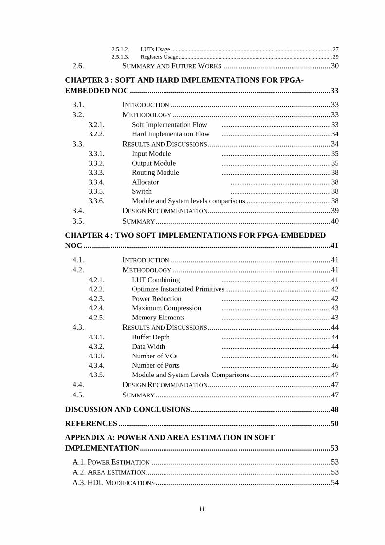
comparison with CONNECT.
Figure 2-16: Packet Format of Split-Merge and CONNECT Networks
21
Results in Table 2-6 show that Split-Merge has the advantage of higher speed, but
with the cost of more area consumption.
Table 2-6: Implementation Results for CONNECT & Split-Merge [12]
Register Logic
(LUT)
Memory
(LUT)
Frequency
MHz
CONNECT
1 clock
2VC; 32bit 685 1369 066 104
2VC; 64bit 0265 1926 288 92
Split-Merge
1 pipe
2 clocks
DOR; 32bit 540 1449 336 220
DOR; 42bit 641 1686 462 219
WSF; 32bit 579 1839 400 217
WSF; 42bit 679 2139 550 216
Split-Merge
2 pipe
4 clocks
DOR; 32bit 1262 1157 336 303
DOR; 42bit 1572 1302 462 201
WSF; 32bit 1545 1491 400 298
DOR; 42bit 1804 1666 5501 213
Simulation results in Figure 2-17 show that under low congestion CONNECT
works with lower average delay. On the other hand, Split-Merge achieves higher
performance under congested traffic.
Figure 2-17: Cycle Comparison between CONNECT and Split- Merge PS NoC
[12]
2.4.8. FLNR
A. Imbewa and M. A. S. Khalid [13] introduced a fast lightweight NoC router
designed for FPGAs with the objectives of using minimum resources and obtaining
high performance.

21
Packet has been modified to minimize the control fields, by removing the control
fields from its body and removing the tail flit as shown in Figure 2-18. This yields to
FIFO width reduction, so buffer area and power consumption will be reduced as well.
Figure 2-18: FLNR Packet Format
In FLNR design, the router decision time is only one clock cycle; also it takes one
clock cycle to write the body flits since credit-based flow control is used. This yields to
buffer depth reduction and high performance.
As shown in Figure 2-19, each router is connected to the surroundings (North,
East, South, and West) IPs/routers, as well as the local IP core.
Figure 2-19: FLNR Block Diagram [13]
FLNR components and their functionalists:
Arbiter: It receives the notifications (flit headers that contain packet
information including destination address) coming from input ports and
serves them in North, East, South, West, and Local orders using Round
Robin. Also it detects the head flit and payload end.

22
Direction Decoder: It receives the destination address of the packet and
calculates the routing directions using XY routing (the cheapest schema to
have deadlock free network).
FIFO Depth: The minimum depth is the number of possible flits that are
stored during routing decision time. If there is no blocking, only two
buffers (one for head flit, one for body flit) are enough to get the minimum
latency.
Switch: Finally the switch assigns the coming packets from input ports to
available channels. Simply the switch is a five 5–to-1 multiplexers that
support all possible connections between input and output buffers.
Router parameters are input buffer size and flit size.
FLNR was implemented on Altera Stratix II EP2S15F672I4 FPGA. The synthesis
results for FLNR with three hops and buffer size of eight flits are shown in Figure 2-20.
Figure 2-20: Synthesis Results for FLNR [13]
The comparison with other routers (HERMES [14], ICN [15] and Bartic [16]) is
done by calculating the port bandwidth (maximum throughput) for each design, then
calculating the best case latency based on the same case study. Figure 2-21 and Table
2-7 give the comparison results. FLNR significantly outperforms the other routers with
lower area, latency and higher frequency. Furthermore, the number of clock cycles
consumed to finish the routing decision ( ) is only one cycle.

23
Figure 2-21: FLNR Performance and Area Comparison with some Previous NoC
Routers [13]
Table 2-7: FLNR Performance and Area Comparison with some Previous NoC
Routers [13]
Design Flit Size Flit/Cycle Slices Frequency
(MHz)
BW
(Mbps)
HERMES
[14]
8 0.5 406 25 10 100
ICN [15] 16 0.5 326 40 2 320
Batric [16] 16 1 807 50 3 800
FLNR 8 1 150 54 1 435
2.4.9. RROCN
HY. Luo, SJ. Wei, and DH. Guo [17] introduced an on-chip network with regular
reconfigurable topology (RROCN) which contains both routed network and shared bus
by disabling and bypassing the unwanted nodes of the routed network and reorganize
them as a shared bus, this leads to suitable throughput and power consumption for
application with different bandwidth demands.
The main goal of RROCN is to provide a reconfigurable suitable bandwidth NoC
with low cost.
The RROCN architecture consists of several nodes, each one contains a router,
where a CPU core is attached to the network through the local port of the router while

24
the peripherals are located around the network which gives a NxN 2D mesh topology as
the largest topology that RROCN constructs with different MxH shapes but must be
less than N.
The main components of RROCN router are shown in Figure 2-22.
Figure 2-22: RRCON Router Block Diagram [17]
PRCON components functionalities:
Reconfiguration Controller: configures the crossbar and the multiplexers
using the information that is received from the previous router, after that it
generates new configuration information which is passed to the next router.
Crossbar: responsible for connecting the input port to the output port of the
router. It consists of five ports. One for local port and the others are
processor and peripheral group as shown in Figure 2-23.
Arbiter: handles only the requests from the peripherals group and constructs
the connections for it using the priorities inside the configuration
information.
Figure 2-23: RRCON Crossbar Architecture [17]
The reconfiguration process is started at the run time from the processor by first
selecting an original node to be the starting point of the network, and then the
configuration information spreads inside the network to reach each node using

25
reconfiguration controllers in each node using an YX constructive algorithm. After
constructing the network, a modified self-adaptive XY routing algorithm is used.
As shown in Table 2-8, hybrid circuit switching NoC is compared with the
RROCN in terms of area, power consumption, clock period, latency and maximum
throughput in four configurations. Four configurations topology, the coordinate
(1,1,1,1) based on the original node 44 is defined as 1111_44.
Table 2-8: RRCON Implementation Results on Four Configurations [17]
0000_00 0000_33 3030_11 0000_11
Larger clock period
(%)
104.0 35.9 37.4 9.7
Less power
consumption )%(
5227 5928 4028 0420
Lower zero-load
latency with equal
frequency (%)
7728 7824 8425 0420
Lower zero-load
latency with
maximum
frequency (%)
5427 6828 0121 528
Lower maximum
frequency (%)
5021 2624 5224 2829
2.5. Comparative Review between NoCs with Open-Source
Code
In this section, we select the NoC designs [4], [9] and [10] with available open
source code, make our comparison between them and analyze their operating
frequencies, FPGA resources allocation across different values of buffer depth, data
width and VCs numbers to help selecting the suitable NoC that fits system
requirements.
2.5.1. Comparison Work Flow
We compare between the three architectures across different numbers of VCS, data
width and buffer depth and analyze their effects on frequency and LUTs and registers
usage. Network configuration is 4x4 mesh topology with five input and output ports.
The routers are implemented using Xilinx ISE v14.4 tool targeting Virtex6
XC6VLX240T FPGA. During the synthesis stage, RAM extraction option is disabled
to guarantee fairness among the three routers.
2.5.1.1. Frequency
Buffer Depth: Increasing buffer depth improves the capability of storing
more packets. Consequently, this adds extra logic to handle the queuing

26
process and decreases the operating frequency. Figure 2-24 shows that
NoCem has the highest operating frequency across all values of buffer
depth and it is the most sensitive router to changes in buffer depth.
Figure 2-24: Frequency vs Buffer Depth
Data Width: Data width change does not have high impact on the operating
frequency of the three routers as shown in Figure 2-25. CONNECT is the
most sensitive router to this parameter, whereas SOTA operating frequency
is almost fixed. NoCem is the router with the highest operating frequency
for all data width values.
Figure 2-25: Frequency vs Data Width

27
Number of VCs: As shown in Figure 2-26, increasing VCs decreases the
operating frequency for all routers because adding VCs leads to more
combinational delays of switching algorithms and arbiters. NoCem has the
highest operating frequency, however it supports only up to four VC.
CONNECT is the most sensitive router to VCs increase.
Figure 2-26: Frequency vs VC
2.5.1.2. LUTs Usage
Buffer Depth: From Figure 2-27, for all values of buffer depth, SOTA
consumes the least number of LUTs, whereas NoCem has the largest LUTs
consumption.

28
Figure 2-27: LUTs usage vs Buffer Depth
Data Width: Increasing data width does not introduce extra logic, so this
parameter does not have high impact on number of LUTs used for logic
implementation. As shown in Figure 2-28, for 8 and 16 bits data width,
NoCem is the most efficient in LUTs consumption, whereas it consumes
the largest number of LUTs when the data width is 32 bits.
Figure 1-28: LUTs usage vs Data Width
Number of VCs: Adding VCs introduces more logic for routing
computation, which increases LUTs consumption. Figure 2-29 shows that

29
NoCem consumes more LUTs than SOTA and CONNECT for all VCs
numbers. For VC count larger than three, SOTA consumes less LUTs than
CONNECT.
Figure 2-29: LUTs usage vs VC
2.5.1.3. Registers Usage
More memory elements are needed with the increase of any of the three parameters
(buffer depth, data width and number of VCs) as shown in Figures 2-30, 2-31 and 2-32.
SOTA is the most efficient in registers consumption and NoCem consumes the largest
number of registers.
Figure 2-30: Registers usage vs Buffer Depth

31
Figure 2-31: Registers usage vs Data Width
Figure 2-32: Registers usage vs VC
2.6. Summary and Future Works
PNoC [3] is a circuit-switched approach applied to FPGA-based systems. It
provides a flexible, lightweight and easy design. Its performance is similar to direct
interconnect. PNoC design can be used for partial dynamic reconfiguration by updating
the routing table of the system with added and removed modules. But on other hand; it
will not be suitable for applications subjected to conflicting flows, since in the circuit-
switched connections, once established, no other modules are able to communicate.

31
Future work is to explore the use of multiple routers, topologies and subnets in a
system. Perform a detailed comparison with packet-switched NoCs. And apply more
tests to check its suitability for partial dynamic reconfiguration.
The configurable [7] router provides the flexibility in supporting a variety of
network topologies with a simple three bit input for configuration. A dual crossbar
arrangement gives lower area with some reduction in operating frequency.
In future work, router's configuration is improved to include:
Virtual channels to achieve higher throughput under conditions of high
traffic congestion.
Using the concept of middle-buffering to achieve smaller designs and
superior performance than output buffering.
Using custom memory block for buffer implementation.
In [12], detailed comparison between Split-Merged PS approach and CONNECT
has been introduced using different sets of benchmarks. Results show that Split-Merged
PS system reaches up to 300 MHz which is three times higher frequency and
throughput than CONNECT but with an increase in area usage.
FLNR [13] is a NoC router for FPGA that minimizes the area, maintains fast
performance by minimizing the control fields in the packets to decrease the buffer
width, decreases the routing decision time and delivers each flit in one clock cycle.
Future work is to implement a dual-clock wormhole router to forward the body flits
at faster frequency than the head flits.
Also, we think that authors should consider comprising FLNR results with more
recent NoC approaches e.g. CONNECT and SOTA. Since there is no open source code
for FLNR, we could not make this comparison.
RROCN [17] is proposed for chip-multiprocessors to achieve lower power
consumption under a demanded throughput. The RROCN was evaluated with four
specific reconfiguration topologies and compared with HCS network. RROCN is
suitable for specific applications, for example if we have application with specific
throughput demand, the RROCN is configured with a topology that provides suitable
throughput with less power consumption and lower zero-load latency and the same
thing happens if we have application requires lower latency or less power consumption.
The reconfiguration process is used to compromise between throughput, latency and
power consumption or optimize for one of them.
Future work was to improve the router design to include other network topologies
other than mesh topology and make further optimization to increase the maximum
throughput using the concept of virtual channels.
In this chapter, we also have compared between three NoC from the respective of
maximum operating frequency, registers consumed as memory elements and LUTs for
logic computation across three NoC parameters which are data width, buffer depth and
number of VCs. The comparison results help in choosing the appropriate NoC
according to system requirements:
If the operating frequency is the most important factor, NoCem is the best
choice with the cost of more LUTs consumption with increasing buffer
depth or number of VCs.

32
For networks with small numbers of VCs, CONNECT is the most efficient
in LUTs consumption. On the other hand, it has the lowest operating
frequency across all NoC parameters.
If the target is improving the QoS of the network, this means that increasing
number of VCs is needed and SOTA is the most suitable router. As we
increase data width, buffer depth or VCs, it consumes the least amount of
registers. Increasing data width in SOTA is more suitable in case of
requiring high data transfer rate.

33
Chapter 3 : Soft and Hard Implementations for FPGA-
Embedded NoC
3.1. Introduction
We study the behavior of FPGA-embedded CONNECT NoC sub-modules which
are input, output, router, allocator and switch; while changing the NoC parameters
which are data width, buffer depth and number of VCs and ports. With every run, we
change a single parameter and keep other parameters fixed, then measure the area,
delay and dynamic power gaps between soft and hard implementations.
3.2. Methodology
Five input and output ports, two VCs, 32 bits data word and 10 words buffer are
the baseline values of NoC parameters.
For soft implementation, Virtex5 FPGA (xc5vlx110t) [19, 20] is used and UMC’s
65 nm ASIC process technology [21] is used for hard implementation. UMC’s65nm
technology is selcted to follow the same methodology in [22, 23]. One FPGA from
Virtex5 family is used because of two reasons. 1) This family is fabricated by 65nm
process technology and 2) the availability of area resources of this family in [24, 25].
Table 3-1 shows FPGA resources with the equivalent silicon area.
Table 3.1: Estimated FPGA Resources Area
Resource Equivalent Number of
Gates
Silicon Area in mm2
Register 7 0.000341
LUT 24 0.001171
IO 100 0.004882
BRAM - 0.025436
3.2.1. Soft Implementation Flow
The used software for soft implementation is ISE v14.4. We force the tool to reach
the maximum available frequency by:
1- Setting time constraints to high frequency (1 GHz)
2- Using all available speed optimization options
3- Applying physical synthesis [26] to decrease the critical path with the cost of
small area increase.
Only the clock signal at the top module is connected to IO buffers, because in
integrated system, all input and output signals will be connected to their corresponding
signals of other routers based on the NoC configuration.

34
The tool calculates area utilization and maximum frequency after every stage. We
are only concerned with results after place and route (PAR) because of their accuracy
after this stage. Also, because combining and packing FPGA resources due to
optimization options are taken into account after PAR. Exact routing and component
delays are generated in this stage.
Dynamic and static power consumptions [27] are measured using integrated tool
within ISE called xPower Analyzer [28]. For power extraction, the tool uses:
- The Native Circuit Description File (NCD) file. It is generated after PAR
and describes the physical design of the FPGA.
- The Physical Constraints (PCF) file. It is created during mapping stage and
consists of two sections. The first part includes the physical constraints
created by the mapper. The second section is for the physical constraints
specified by the user. Information in PCF file is used to determine clock
frequencies. And providing it to xPower Analyzer tool is very important for
accurate estimation of dynamic power consumption.
3.2.2. Hard Implementation Flow
Synopsys design compiler 2008.09 is used for hard implementation with typical
case process library and 1V supply voltage. The used wire load model is endorsed
model.
In soft implementation, the components of the FPGA are fixed and the used
resources are selected according to the design and its constraints. While on hard
implementation the used constraints affect dramatically the area utilization especially
on buffers insertion and cells upsizing. That is why the area, delay and power results
are gathered across two steps. At first, we set the tool with very tight timing constraints,
enable the “scan” option to get more realistic timing measurement and use ultra-
compilation for high optimization of area and clock. The scannable flip-flops replace
the non-scannable flip flops during compilation. At the end of this step the value of
negative slack is extracted from timing reports generated by the tool. In the second step,
these negative slack values are used as a target for timing constraint. Then after
recompilation, area and power consumptions are extracted. And the final delay
measurement takes into account if there is a positive or negative value for the slack.
3.3. Results and Discussions
CONNECT requires data buffering to store flits till the destination is ready to
receive packets and to store routing tables and other information required for successful
transmission. 2D flip flop array is always used to implement memory buffers on ASIC.
FPGA has three types of resources that can be used as memory elements [29]. These
resources are:
1- Register: it is a group of flip flops for storing a bit pattern. Consequently, when
registers are used for data storing, there is no waste at all.
2- Distributed RAM (DRAM): look up tables (LUTs) are normally used for logic
functions, but LUTs can be grouped together and configured as small memory
elements called DRAMs.

35
3- Block RAM (BRAM): it is a dedicated component in the FPGA for storing
data.
3.3.1. Input Module
Input module is responsible of
- Logic calculations required for data control and routing
- Memory buffers for storing the data coming to the router till its destination
is ready for receiving.
This module was implemented to target only DRAM but we modified it so that its
memory buffers can target the three buffering options in soft implementations.
Figures 3-1a, 3-1b and 3-1c show area utilization of input module across the three
buffering options with changing buffer depth, data width and number of VCs.
Register is not the suitable selection for implementing memory buffers because
number of registers increases rapidly specially with data width increase.
Under small values of buffer depth, data with and number of VCs, there is a small
increase of DRAM area consumption than BRAM, but with increasing any of them,
DRAM becomes worse than BRAM. On the other hand BRAM area consumption is
almost constant across the parameters.
The disadvantages of using BRAM and DRAM is the possibility of bits waste of
these resources if the module instantiated them without using all their bits.
So based on silicon area results shown in Figures 3-1a, 3-1b and 3-1c, BRAM is
the most suitable choice for input module across all parameters followed by DRAM
under small values of buffer depth, data width and number of VCs.
Comparing input module using BRAM implementation with other modules, it
depends on data width, buffer depth and VCs number. It has the least gabs in area,
delay and power as shown in Figures 3-2, 3-3 and 3-4. Increasing data width and buffer
depth reduces power and area gaps. While adding more VCs adds more delay gap but
decreases area and power gaps.
3.3.2. Output Module
Output module is independent on data width and the number of VCs. While it
changes with buffer depth and number of ports with more sensitivity to buffer depth
than number of ports because with buffer depth increase, more registers and
combinational logic are required which justifies the large power and area gabs as shown
in Figures 3-2, 3-3 and 3-4.

36
Figure 3-1: FPGA memory buffers using three implementation alternatives
Figure 3-2: FPGA/ASIC Area Ratios

37
Figure 3-3: FPGA/ASIC Delay Ratios
Figure 3-4: FPGA/ASIC Power Ratios.

38
3.3.3. Routing Module
Routing module consists of
- Logic part for determining routing paths.
- Memory buffers that are used to hold information about available input and
output ports.
We modified this module so that its memory buffers can target the three buffering
options in soft implementations and analyzed their behaviors with changing number of
ports. Figure 3-1d shows that starting from four ports; DRAM is the best choice for this
module since it has the best silicon area besides that area consumption is almost
constant across all ports numbers. This is because routing module use memory buffers
to store information about input and output ports availability which makes the needed
memory size very small compared to input module that holds the data itself besides
other information used for transferring the flits through the network.
Figures 3-2d, 3-3d and 3-4d show FPGA to ASIC ratios for this module with
DRAM memory buffers across available ports numbers. Its area, delay and power
values in hard implementation increase with ports number increase while in soft
implementation, their values are almost fixed across ports numbers. This is because the
resources allocation in FPGA of four ports setup would be the same for five to fifteen
ports setup.
3.3.4. Allocator
This module depends on the number of ports. Its area, speed and power values
increase rapidly in both hard and soft implementations with increasing ports numbers as
shown in Figures 3-2d, 3-3d and 3-4d. But their values increase faster in soft
implementation mainly because of the combinational logic besides that the module
consists of multiple logic elements that communicate with each other using
interconnects which are well known of consuming area and power and increasing the
critical path.
3.3.5. Switch
Because of the pure combinational logic of the switch module, registers were
inserted at the module output. This is mandatory for the tool to force timing analysis.
Switch module depends on the number of ports. As shown in Figure 3-3d, delay gap is
insensitive to ports numbers and is almost fixed. While Figure 3-4d shows that
increasing ports numbers decreases power gap.
3.3.6. Module and System levels comparisons
Geometric means of soft-hard ratios of area, delay and power gaps are shown in
Table 3-2. Geometric mean is the suitable mean for comparing normalized values [30].
Input modules geometric means are 1.8x, 2.9x and 5.3x respectively. These are the
least gaps across all modules. Delay geometric mean for output module is 3.5x and it
has very large area and power geometric means 54.7x and 38.1x.

39
The geometric mean of area gap is 27.3x for routing module; while it has large
delay and power gaps 4.6x and 44.8x respectively. These large gaps may be because of
the restrictions of fixed fabrications of the FPGA which affects the optimization of
placement and routing. While ASIC is much more flexible with more efficient
optimizations options, for example scanning to upsize cells.
Allocator module is more sensitive to the number of ports increase in soft
implementation than hard implementation. That is why it has large geometric mean
67.7x for area, 4x for delay and 38.6x for power.
Switch module has the largest geometric means 90x for area, 7x for delay and
52.8x for power gap. This is because this module is purely combinational and ASIC is
much faster than FPGA in combinatorial logic implementation due to the following:
1- FPGA would need several in series LUTs while in ASIC it is possible to
implement wider input functions with significant decrease in delay than FPGA
due to the fine-grain architecture of ASIC.
2- FPGA has programmable routing structure while ASIC has dedicated routing
structure.
Table 3-2: FPGA/ASIC Ratios
Module FPGA/ASIC Area Ratio FPGA/ASIC Delay Ratio FPGA/ASIC Power
Ratio
Min. Max. Geometric
Mean
Min. Max. Geometric
Mean
Min. Max. Geometric
Mean
Input 1 6 1.8 2.5 3.9 2.9 2.7 17.8 5.3
Output 45.4 67.5 54.4 2.8 4 3.5 23.7 75.4 38.1
Routing 9 135 27.3 3.8 5.4 4.7 14.5 204.4 44.8
Allocator 42.6 82.5 67.7 2.5 5.6 4 28.3 77.1 38.6
Encoder 78.8 129.3 90 7 7 7 41.4 107.3 52.8
Total
Router
2.8 45.2 9 3 4.3 3.7 5.8 425.5 12
3.4. Design Recommendation
1- Routing module needs small memory buffers, so DRAM implementation is
more suitable for this module. On the other hand, input module needs large
memory buffers and BRAM is the best choice for it. The area utilization is
almost similar across different values of VCs number, data width and buffer
depth.
2- To get higher bandwidth for input module, increasing data width is better than
increasing the number of VCs. Also increasing data width reduces area and
power gaps. Area gap is reduced from 6x to 1x and power gap drops from 12x
to 6x. Using small number of VCs increases area and power gaps for input
module.

41
3- It is recommended not to increase the number of ports if the main concern is
the speed results. As shown in Figures 3-2 and 3-3 and Table 3-2, increasing
ports numbers adds significant increase in allocators speed gap (raises from
2.5x to 5.6x) and area gap (changes from 41x to 82x) while the impact on
power gap in not high. Ports numbers change has less effect on encoder and
output modules. On the other hand increasing the number of ports reduces
speed, delay and power gaps of the routing module. Speed gap reduced from
5.4x to 3.8x, power gap falls from 204.5x to 14.5x and area gap changes from
135x to 9x.
4- Given that the switch and the allocator modules have the largest speed, area
and power gaps, they are more suitable to be harden than being soft
implemented. Also this might indicate that more enhancements may be needed
for these modules on soft implementations.
5- Comparing our work with SOTA [9] in Table 3-2 proves that when the NoC is
designed to be FPGA-embedded NoC, it would utilize bandwidth and area
better than NoCs designed to target ASIC (30x area gap and 3.6x speed gap).
3.5. Summary
In this chapter, we provided a comparison on the sub-module level between soft
and hard implementations using FPGA-embedded NoC and measured the efficiency
gaps between the two implementations. In soft implementations, it is more efficient to
use BRAM in input module as memory elements. On the other hand DRAM is more
suitable for routing module. Increasing data width is better than adding more VCs for
better operating frequency. Switches and allocators are not efficient in soft
implementation since they consume large area and power and increase the critical path.
When the NoC is designed to target FPGA, its efficiency gaps in soft
implementation are better than the efficiency gaps of NoC designed for ASIC.

41
Chapter 4 : Two Soft Implementations For FPGA-
Embedded NoC
4.1. Introduction
Our contribution in this chapter is introducing two different configurations for the
soft implementation using the CONNECT FPGA-embedded NoC. In each
configuration, we measure area, speed and power gaps on the network level between
soft and hard implementations. First configuration targets reducing the delay gap
between soft and hard implementations as much as possible, whereas in the second
configuration the soft implementation has significant reduction of consumed power
with the cost of small increase in the delay and area gaps.
4.2. Methodology
We follow the same methodology in previous chapter for soft and hard
implementations.
We study the effect of changing FPGA synthesis, mapping and place and routing
properties on the NoC router besides modifying specific components of the NoC to
reduce the gap between soft and hard implementations. In the first setup, we select
properties and modify specific components to get the least delay gap between soft and
hard implementations. In the second setup, we modify these options and components to
reduce the power gap between soft and hard implementations. Following that, we
measure the effect of these changes on the area and speed gaps. For each setup, we
change one of the NoC parameters which are buffer depth, data width, number of VCs
and number of portsthenmeasuretherouter’sarea,delayandpower.
The following section clarifies the options used for speed-target and power-target
configurations. The two configurations are summarized in Table 4-1.
4.2.1. LUT Combining
The main resources for implementing sequential and combinational logic in FPGA
are“TheConfigurableLogicBlocks(CLBs).EachCLBinVirtex-5 FPGA consists of
two slices. Each slice has four 6-input lookup tables (LUTs), four flip-flops (FFs), three
multiplexers, and a length-4 carry chain comprising of multiplexers and XOR gates.
LUTs are standard elements that are used for executing combinational logic. They work
as a small memory that holds the truth table of outputs for all inputs combinations.
Each 6-input LUT can be used as two 5-input LUT with two outputs; this is called dual
output mode. Therefore, each slice can be used to either implement one function with
six inputs or two independent functions sharing five or less inputs with two separate
outputs. This will reduce the required resources of LUTs for circuits that consist of
small logic functions, giving better utilization with less dynamic power consumption.
Unfortunately this causes performance degradation.
Dual output mode can be enabled or disabled using LUT combining option in
synthesis and mapping stages [31, 32]. It may be disabled or may be set with two other

42
values called “Area” and “Auto”. Setting it to “Area” combines LUTs as much as
possible ignoring the resulted performance degradation. On the other hand, setting it to
“Auto” balances between area optimization and design speed. For power-target
configuration, this option is set to “Auto” during synthesis; and set to “Area” in
mapping stage. These selections are based on multiple tests that showed that this
combination compromises between saving the power as much as possible with
reasonable performance degradation. Other combinations don not improve power
consumption. On the other hand, they have negative impact on the design operating
frequency and cause more performance degradation. In speed-target configuration; the
option is disabled in both synthesis and mapping to avoid any performance degradation.
4.2.2. Optimize Instantiated Primitives
Most FPGA vendors provide various synthesis options that have remarkable effects
on the designs results [33]. In most of the cases, setting the options is enough for the
FPGA to follow the set rules. However in some cases, setting the synthesis options is
not enough and designers must rewrite the HDL code to force insertion of specific
FPGA components [34]. Better method is to target FPGA-embedded primitive
instantiation. This method is effective for design optimization and sometimes it
becomes the only way to achieve the required target or to make work around a bug in
the synthesis tool. In addition, it makes the design less dependent on the synthesis tool.
On the other hand, the design will be more difficult to maintain and less portable.
Practically these disadvantages have less impact on designs because in most of the
cases, the target FPGA is already defined before writing the HDL code. Moreover,
most of the new FPGA families provide backward compatibility to older FPGA
versions. One example of the manual instantiation is to force the distributed RAM to be
used instead of the BRAM to save power.
The tool does not optimize instantiated primitives unless this synthesis option is set
to“True”[31]. This optimization is limited by multiple conditions [35]. For example, if
there are specific constraints like Relative Location Constraints (RLOC) applied on
those instantiated primitives, no optimization will be conducted. Also the tool does not
optimize some hardware elements such as BRAM and DSP48. This option is disabled
in speed-target configuration and enabled in power-target configuration.
4.2.3. Power Reduction
Using the default settings; the tool attempts to reduce the consumed power.
Performance, area, power and runtime are the different strategies that can be applied by
the tool. According to the selected strategy, the tool applies the proper algorithms for
power reduction. Because of the trade-offs between these strategies, user should
configure the tool with the most important strategy according to his design
specifications.
The tool provides power reduction switches in synthesis, mapping and routing
stages to enhance power results at the expense of longer run time, performance
degradation and sometimes more area consumption. The general rule in the relation
between power and area results is that the function would consume less power as long
as it uses fewer resources for its implementation. However in some cases there is a

43
contradiction between them; because there are power reduction algorithms that require
more logic or resources [36].
At synthesis stage, the tool has different algorithms for power reduction that can be
applied globally, per module or per function. At mapping stage; the tool works on
improving the placement to achieve less power consumption. It starts with choosing a
layout for the design that satisfies timing constraints, and then runs time analysis to
check if there is timing slack. If timing slack is found, the tool modifies the placement
to get better results. At PAR stage; the tool works first on meeting timing constraints;
then reducing power on nets that are not part of the critical path. This stage also
includes optimizations of logic that does not affect functionality or timing but achieves
better power results. In other words mapping minimizes routing by enabling time
driven packing and PAR reduces power consumption by optimizing routing.
Mapping and PAR power reduction options yield to improving power results with
10-15% [37]. However these options increase the running time by 15% with
performance degradation. As long as the timing constraints are tighter, power
reductions algorithms will not be able to make sufficient changes in order not to affect
timing. Power reductions options in the three stages are disabled in speed-target
configuration and enabled in power-target configuration.
4.2.4. Maximum Compression
It is a mapping option that packs the logic of the design with the most possible
density [32]. This saves area and power consumption with the cost of performance
degradation. This option is enabled in power-target configuration and disabled in
speed-target configuration.
4.2.5. Memory Elements
One of the experiments implemented in previous chapter is using three different
implementations for memory elements. In each implementation, area consumption of
each component was measured across NoC parameters. These three implementation
target Registers, DRAMs and BRAMs respectively. Results showed that using registers
as memory elements is not efficient at all across all parameters. BRAM is the most
efficient implementation for input module specially with increasing buffer depth, data
width and number of VCs. DRAMs is more suitable for routing module because this
module needs small memory elements for storing the information of available input and
output ports. In speed-target configuration, input module is modified to target BRAMs,
whereas in power-target configuration the module uses DRAMs.
Table 4-1: Speed and Power Target configurations
Option Stage Speed-target Power-target
LUT Combining
Synthesis Off Auto
Mapping Off Area
Optimize Instantiated
Primitives
Synthesis Disabled Enabled

44
Maximum Compression Mapping Disabled Enabled
Power Reduction Synthesis Disabled Enabled
Mapping Disabled Enabled
PAR Disabled Enabled
4.3. Results and Discussions
4.3.1. Buffer Depth
The simulation results in previous chapter showed that output and input
components depend on changing buffer depth parameter. Moreover, output module in
soft implementation consumes more area and power than hard implementation at small
buffer depths. As previously mentioned; in speed-target setup, the input module was
modified so that it can be allocated in BRAMs and in power-target setup, the module
uses DRAMs. Using BRAMs and setting the tool with speed-target configuration make
soft implementation consumes less area than power-target setup for all values of buffer
depth as shown in Figure 4-1. However it comes with a high cost of power
consumption especially for small values of buffer depth (Figure 4-3). This is justified
because using BRAMs consumes more power than DRAMs. Figure 4-2 shows that
starting from 30 words buffer depth the two setups have similar delay gap and for
values less than 30 words speed-target setup has less delay gap than power-target setup.
4.3.2. Data Width
Input module is the component that depends on data width changes. For small
values of data width, area consumptions of BRAMs and DRAMs are close and with
increasing data width, DRAMs start consuming more area. This justifies Figure 4-1
where speed-target and power-target setups have similar area ratios for small data
width; then for higher data width, the area gap increases in power-target setup. Using
BRAMs in speed-target setup and DRAMs in power-target setup illustrate Figures 4-2
and 4-3 where in speed-target setup the soft implementation has less delay and
consumes more power.

45
Figure 4-1: Speed vs Power Setups FPGA/ASIC Area Ratios
Figure 4-2: Speed vs Power Setups FPGA/ASIC Delay Ratios.

46
4.3.3. Number of VCs
Input component depends on the used number of VCs. Similar to the data width
analysis that has just been covered; for small numbers of VCs, BRAMs and DRAMs
consume similar amount of resources, BRAMs are more efficient with increasing VCs.
Number of VCs does not affect the output component itself. However number of
created instances of the module depends on the number of VCs. Figures 4-1 and 4-2
show that speed-target setup has more area consumption and better performance than
power-target setup. However their values are still close to each other. But from power
respective, power-target setup satisfies high power reduction across all numbers of VCs
due to using DRAMs for input module in this setup.
4.3.4. Number of Ports
All NoC components except the input component depend on the number of ports.
Number of created instances of all components depends on number of ports except the
allocator module; one instance of it is created for the whole router. Results in Figure 4-
1 show that across all components, changing number of ports for speed-target and
power-target setups does not have high impact on area. From Figure 4-2, speed-target
setup has better performance results than power-target setup. From power respective
soft implementation in speed-target setup consumes almost the double values of power-
target setup as shown in Figure 4-3.
Figure 4-3: Speed vs Power Setups FPGA/ASIC Power Ratios

47
4.3.5. Module and System Levels Comparisons
Minimum, maximum and geometric means of area, delay and power gaps for soft
and hard implementations at both speed and power target setups are shown in Table 4-
2. Setting FPGA with speed-target configuration reduces the delay gap to a factor of
5.5x between soft and hard implementations with a very high cost of the power
consumption 12.2x and 5.9x area usage. Configuring the FPGA with power-target setup
decreases the power gap to only 4.5x with a small increases in the speed and power
gaps 6.3x and 6.9x respectively.
Table 4-2: Speed vs Power Setups FPGA/ASIC Ratios
Setup FPGA/ASIC Area Ratio FPGA/ASIC Delay Ratio FPGA/ASIC Power
Ratio
Min. Max. Geometric
Mean
Min. Max. Geometric
Mean
Min. Max. Geometric
Mean
Speed-
Target
2.8 21.4 5.9 3.5 10.4 5.5 6 24.9 12.2
Power-
Target
4.2 20.2 6.9 3.8 12.8 6.3 1.7 13 4.5
4.4. Design Recommendation
Based on the previous results; for applications that are concerned with reducing the
delay gap as much as possible between soft and hard implementations, speed-target
options in Table 4-1 are recommended be used for soft implementation. But this will
increase the power consumption gap to by a factor of 12.2x. This power gap can be
reduced from 12.2x to only 4.5x with the cost of increasing the delay gap from 5.5x to
6.3x and increasing the area gap from 5.9x to 6.9x. The power reduction can be fulfilled
by configuring the FPGA with power-target options in Table 4-1 besides using DRAMs
for input module instead of using BRAMs. Power-target configuration is more
appropriate for applications with power limitations.
4.5. Summary
We choose FPGA-embedded NoC and propose two configurations for soft
implementation. In each configuration we analyze efficiency gaps between soft and
hard implementations on network level. One configuration targets the minimum delay
gap (5.5x) between soft and hard implementations, this leads to 12.2x power gap and
5.9x area gap. The other configuration targets reducing the power gap to 4.5x, leading
to 6.9x area gap and 6.3x delay gap. Choosing the appropriate configuration depends on
the application type. It is recommended to use the power-target configuration for
applications that require power saving, since the impacts on the area and delay gaps are
limited.

48
Discussion and Conclusions
Integrating NoCs within FPGAs becomes a main factor for improving data
communication especially for high speed IOs interfaces, and partial dynamic
reconfiguration and for improving bandwidth utilization, decreasing the compilation
time and increasing designs efficiency and scalability.
The thesis contribution is in three phases. In Chapter 2, there is an overview about
networking principles then, provide a survey of the following NoCs routers:
NoCem
PNoC
Dual Crossbar Router
HW NoC
SOTA
CONNECT
Split and Merge PS
FLNR
RROCN
For these NoCs, we show their architectures, implementations, simulation, test
results and future works. Then we make our comparisons using a unified
implementation for NoCs with available open-source code which are NoCem, SOTA
and CONNECT. The comparison analyzed the behavior of the three NoCs operating
frequencies and resources utilization of LUTs and registers across different values of
the NoC parameters which are data width, buffer depth and number of VCs to help
choosing the suitable NoC design according to target applications. Results show that:
NoCem has the highest operating frequency advantage. On the other hand,
it consumes more LUTs with increasing number of VCs or buffer depth
CONNECT has the lowest operating frequency for all NoC parameters. For
networks with low number of VCs, it consumes the least amount of LUTs
SOTA consumes the least amount of registers with increasing buffer depth,
data width or number of VCs
In Chapter 3, we use FPGA-embedded NoC (CONNECT) and study its behavior
on the sub-module level in soft and hard implementations. Based on analyzing the
power, area and delay of each module in soft and hard implementations across different
values of buffer depth, data width, number of VCs and number of ports, we give design
guidelines for embedded NoCs on FPGAs.
For soft NoCs, using BRAMs for input modules gives high area utilization while
LUTRAMs are more suitable for routing module. To utilize bandwidth, it is better to
increase the data width than increasing the number of VCs or ports. Allocators and
switches have larger area, delay and power in soft implementation which make them
unsuitable for soft implementation. NoCs designed for FPGA in soft implementations
would utilize area better than NoCs designed for ASIC.
Finally in Chapter 4, we use the same FPGA-embedded NoC and propose two
configurations for the soft implementation. The differences between the two
configurations are in the following parameters:

49
“LUT Combining” in synthesis and mapping stages
“Optimize Instantiated Primitives”
“Maximum Compression”
“Power Reduction” in synthesis, mapping and PAR stages
“RAM Extraction” for Input Module
For each configuration, the NoC efficiency gaps on the network level for soft and
hard implementations have been analyzed. One configuration attempts minimizing the
delay gap between soft and hard implementations. The second configuration targets
reducing the power gap as much as possible with a limited increase for area and delay
gaps. System constraints
According to system constraints, the relevant configuration will be used for FPGA
setup.
Many of the experiments, results and their conclusions in this thesis are published
in [38, 39 and 40].
As extension to this work, the following points are recommended for the future
work:
According to the results of the sub-module level efficiency gaps, design a
new FPGA-embedded router optimized for soft implementation.
Measure the efficiency gaps at the sub-module level between soft and hard
implementations using different technologies and analyze the effect of
changing the technology on the results.
Modify the FPGA-embedded NoC to include the Round Robin arbiter
proposed in [41], then measure its effect on the NoC efficiency gaps.
Investigate the ability to develop a hybrid NoC with specific modules in
hard implementation and the other modules in soft implementation.
Upgrade the FPGA-embedded router to perform its functionality as 3D-
NoC for FPGA, then identify whether hard or soft implantation is the best
choice for 3D routers.
Evaluate modifying the router to eliminate using buffers for flow control or
buffering, since measurements in previous chapters show that buffers in the
networks on chips consume significant area and power and increase the
design complexity. Bufferless routers handle contention by deflecting or
dropping flits which leads to a simpler flow control mechanism and no
deadlock or livelock, however this approach reduces the bandwidth and
increases the latency; besides increasing the buffering complexity at the
receiver side because flits may reach their destinations out of order.

51
References
1. ARM:“Ambaspecification”, Technical report, ARM, Revision 2.0, 1999
2. Coreconnect:“Coreconnectbusarchitecture”, Technical report, IBM Cooperation,
1999
3. C. Hilton and B. Nelson. “PNoC: A Flexible Circuit-Switched NoC for FPGA-
based Systems”, IEE Proceedings Computers and Digital Techniques, Vol. 153, pp.
181-188, 2006.
4. E. Bolotin, I. Cidon and R. Ginosar, “Cost Considerations inNetwork onChip”,
Integration, the VLSI Journal, Vol. 38, pp. 19-42, 2004.
5. G.SchelleandD.Grunwald,“ExploringFPGAnetworkonchip implementationsacross various application and network loads”, international conference on Field
Programmable logic and applications, pp. 41–46, 2008.
6. F. Moraes, A. Mello, L. Möller, L. Ost and N. Calazans. “Hermes: an Infrastructure
for Low Area Overhead Packet-Switching Networks on Chip”, Integration, the
VLSI Journal, Vol. 38, pp. 69-93, 2004.
7. R.PauandN.Manjikian,“Implementationofaconfigurable router for embedded
network-on-chip support in FPGAs”, M.Sc. Thesis, College of Engineering,
Queen’sUniversity,Kingston, Ontario, Canada September 2008
8. K.Goossens,M.Bennebroek3,J.Y.HurandM.A.Wahlah,“HardwiredNetworks
on Chip in FPGAs to Unify Functional and Configuration Interconnects”, NOCS
'08 Proceedings of the Second ACM/IEEE International Symposium on Networks-
on-Chip, pp. 45-54, 2008.
9. Daniel U. Becker. “Efficient Microarchitecture for Network-on-Chip Router”,
Ph.D. dissertation, Stanford University, 2012.
10. M. K. Papamichael and J. C. Hoe, “CONNECT: Re-Examining Conventional
Wisdom for Designing NoCs in the Context of FPGAs”, 20th ACM/SIGDA
International Symposium on FPGA, pp. 37–46, 2012.
11. M.K.PapamichaelandJ.C.Hoe,“CONNECT:CONfigurable NEtwork Creation
Tool”, http://users.ece.cmu.edu/mpapamic/connect/ , 2012.
12. Y. Huan1 and A. DeHon2, “FPGA Optimized Packet-Switched NoC using Split
and Merge Primitives”, IEEE International Conference on Field-Programmable
Technology, pp. 47-52, 2012.
13. A. Imbewa and M. A. S. Khalid. FLNR: “A Fast Light-Weight NoC Router for
FPGAs”, Research Centre for Integrated Microsystems (RCIM), Department of
Electrical and Computer Engineering, University of Windsor, pp. 445-448, 2013.
14. F. Moraes, A. Mello, L. Möller, L. Ost and N. Calazans. “Hermes: an Infrastructure
for Low Area Overhead Packet-Switching Networks on Chip”, Integration, the
VLSI Journal, Vol. 38, pp. 69-93, 2004.

51
15. T. Marescaux, T. Bartic, D. Verkest, S. Vernalde and R. Lauwereins.
“Interconnection Networks Enable Fine-Grain Dynamic Multi-Tasking on FPGAs”,
International Conference on Field-Programmable Logic and Applications, pp. 795-
805, 2002.
16. T. Bartic, J-Y. Mignolet, V. Nollet, T. Marescaux, D. Verkest, S. Vemalde and R.
Lauwereins. “Highly Scalable Network on Chip for Reconfigurable Systems”, Proc.
IEEE International Symposium on System-on-Chip, pp. 79-82, 2003.
17. HY. Luo, SJ. Wei, and DH. Guo, “RROCN: An on-chip network with regular
reconfigurable topology for chip-multiprocessors”, Journal of computers, No.1, pp.
36-46, 2013.
18. Helal, K. A., S. Attia, T. Ismail, and H. Mostafa, "Comparative Review of NOCs in
the Context of ASICs and FPGAs", ISCAS, pp. 1866-1869, 2015.
19. XilinxInc.,”Virtex-5FamilyOverview”,2009.
20. XilinxInc.,”Virtex-5FPGAUserGuide”,2012.
21. UMC, “UMK65LSCLLMVBBR_B UMC 65nm Low-K Multi-Voltage Low
LeakageRVTTaplessStandardCellLibraryDatabook”,2011
22. M.S.AbdelfattahandV.Betz,“DesignTradeoffs for Hard and Soft FPGA-based
Networks-on-Chip”, FPT, pp. 95–103, 2012.
23. M.S.AbdelfattahandV.Betz,“THEPOWEROFCOMMUNICATION:Energy
efficient NOCs for FPGAs”, FPL, pp. 1–8, 2013.
24. https://www.xilinx.com/training/downloads/what-is-the-difference-between-an-
fpga-and-an-asic.pptx
25. F.Arnaudet.al.,“AFunctional0.69 Embedded 6T-SRAM bit cell for 65nm
CMOS platform”, the Digest of Technical Papers of the Symposium on VLSI
Technology, pp. 65-66, 2003.
26. XilinxInc.,“PhysicalSynthesisandOptimizationwithISE9.1i”,2007.
27. XilinxInc.,“Virtex-5FPGASystemPowerDesignConsiderations”,2008.
28. www.csee.umbc.edu/~tinoosh/cmpe691/slides/power-estimation.ppt
29. XilinxInc.,“Virtex-5LibrariesGuideforHDLDesigns”,2011.
30. http://www.investopedia.com/terms/g/geometricmean.asp
31. http://www.xilinx.com/itp/xilinx10/isehelp/pp_db_xilinx_specific_options.htm
32. http://www.xilinx.com/support/documentation/sw_manuals/xilinx11/pp_db_map_p
roperties.htm
33. http://www.xilinx.com/support/documentation/sw_manuals/xilinx11/ise_c_xst_perf
ormance_strategies.htm
34. Mourad Fakhfakh, Esteban Tlelo-Cuautle, Patrick Siarry, “Computational
Intelligence in Digital and Network Designs and Applications”, Springer
International Publishing, 2015.
35. Ehliar. A, “OptimizingXilinxdesigns throughprimitive instantiation:Guidelines,
techniques, and tips”, 7th FPGA world Conference, pp. 20-27, 2010.
36. XilinxInc.,“Virtex-5FPGASystemPowerDesignRecommendation”,2008.

52
37. http://www.xilinx.com/support/documentation/sw_manuals/xilinx11/ise_c_xst_pow
er_reduction_strategies.htm
38. Salaheldin, A., K. Abdallah,N.Gamal, andH.Mostafa, “Review of NoC-Based
FPGAs Architectures”, IEEE International Conference on Energy Aware
Computing Systems and Applications, pp. 1-4, 2015.
39. Gamal, N., H. Fahmy, Y. Ismail, and H. Mostafa, "Design Guidelines for
Embedded NoCs on FPGAs", IEEE International Conference on Quality Electronic
Design, pp. 69-74, 2016.
40. Gamal, N., H. A. H. Fahmy, Y. Ismail, T. Ismail, M. Mohie-Eldin, and H. Mostafa,
"Design Guidelines for Soft Implementations to Embedded NoCs of FPGAs", IEEE
International Design and Test Symposium, pp. 1-6, 2016.
41. Helal, K., S. Attia, T. Ismail, and H. Mostafa, "Priority-SelectArbiter:AnEfficient
Round-Robin Arbiter", IEEE International New Circuits and Systems Conference,
pp. 1-4, 2015.

53
Appendix A: Power and Area Estimation in Soft
Implementation
A.1. Power Estimation
As previously mentioned in Chapter 3, xPower Analyzer tool requires two files for
static and dynamic power estimation. First one is the Physical Design File (NCD)
which is mandatory for power estimation. The second file is The Physical Constraints
(PCF). This file is optional, however if this file is not included, dynamic power values
will be almost Zero. Also if this file is included without timing information, dynamic
power values will be inconsistent. A PCF is automatically generated from the User
Constraints File (UCF) by MAP process.
To create UCF in order to generate PCF, use “The Constraints Editor” as follows:
1- In the Processes view, expand User Constraints.
2- Double-click on Create Timing Constraints.
Add the required timing constraints from Constraints Editor as shown
in Figure A-1, then save them using File > Save.
To update the design with the new or modified constraints, run
the Translate process.
Run the MAP process to generate the PFC file.
Figure A-1: ISE Timing Constraint
A.2. Area Estimation
To connect only the clock signal of the top module to IO buffers as mentioned
in 3.2.1, the following steps should be done:
1- In the Process view, right click on Synthesis item and select Process
Properties to open Process Properties Window.

54
2- Press on Xilinx Specific Options, and set Add I/O Buffers to true.
3- Create Xilinx Constraint File (XCF) and set the buffer type property for all the
input and output signals of the top module except the clock to false, then set the
keep property to all signals to true in order not to remove any signals during
optimizations:
BEGIN MODEL <module_name>
NET "signal_name" buffer_type = none;
NET "*" s = true;
END;
4- Open Process Properties Window and enable Synthesis Constraint File
option, then load the XCF file created in previous step.
A.3. HDL Modifications
Input and Routing modules of CONNECT router were implemented to target only
DRAM but we modified them so that their memory buffers can target the three
buffering options in soft implementations.
In this section we show the original memory implementation of the input module
that targets DRAM only, then the modification to the module so that it can target either
BRAM or DRAM
1- Original Implementation:
///////////////////////////////////////////////////////////////////////////////////////////
`ifdef BSV_ASSIGNMENT_DELAY
`else
`define BSV_ASSIGNMENT_DELAY
`endif
module RegFile_1port(CLK, rst_n,
ADDR_IN, D_IN, WE,
ADDR_OUT, D_OUT
);
parameter data_width = 1;
parameter addr_width = 1;
parameter depth = 1<<addr_width;
input CLK;
input rst_n;
input [addr_width - 1 : 0] ADDR_IN;
input [data_width - 1 : 0] D_IN;
input WE;
input [addr_width - 1 : 0] ADDR_OUT;
output [data_width - 1 : 0] D_OUT;
reg [data_width - 1 : 0] arr[0 : depth-1];
always@(posedge CLK)
begin
if (WE)
arr[ADDR_IN] <= `BSV_ASSIGNMENT_DELAY D_IN;
end

55
assign D_OUT = arr[ADDR_OUT ];
endmodule
///////////////////////////////////////////////////////////////////////////////////////////
2- Modified Implementation:
///////////////////////////////////////////////////////////////////////////////////////////
`ifdef BSV_ASSIGNMENT_DELAY
`else
`define BSV_ASSIGNMENT_DELAY
`endif
module RegFile_1port(CLK, rst_n,
ADDR_IN, D_IN, WE,
ADDR_OUT, D_OUT
);
parameter data_width = 1;
parameter addr_width = 1;
parameter depth = 1<<addr_width;
input CLK;
input rst_n;
input [addr_width - 1 : 0] ADDR_IN;
input [data_width - 1 : 0] D_IN;
input WE;
input [addr_width - 1 : 0] ADDR_OUT;
output [data_width - 1 : 0] D_OUT;
reg [data_width - 1 : 0] arr[0 : depth-1];
reg [addr_width - 1 : 0] ADD;
always@ (posedge CLK)
begin
if (WE)
arr[ADDR_IN] <= `BSV_ASSIGNMENT_DELAY D_IN;
ADD <= ADDR_OUT;
end
assign D_OUT = arr[ADD];
endmodule
///////////////////////////////////////////////////////////////////////////////////////////

56
Appendix B: Efficiency Measurements Automation in
Soft Implementation
Chapter 3 and Chapter 4, there have been a huge number of runs for gathering the
efficiency gaps between soft and hard implementations across the network level and
sub-modulelevelamongNoC’sparameters.Doingthis by using the tools in Graphical
User Interface (GUI) mode is very timing consuming and error prone. To save time and
avoid errors, we used the tools in batch mode and automated generating efficiency
parameters by creating scripts written in Tool Command Language (TCL). This
scripting language is already supported by the tools.
ISE generates TCL scripts for creating and running projects. This can be done
through Project menu item then selecting Generate Tcl Script item. We modified
the generated TCL script and created another TCL script to automate calling the
script generated by the tool.
We modified the generated TCL script by ISE in order to be generic and
could be used with different settings as follows:
######################################################
#
# Project automation script
#
# Created for ISE version 14.4
#
# This file contains several Tcl procedures (procs) that you can use to automate
# your project by running from xtclsh or the Project Navigator Tcl console.
# This script is generated assuming your project has HDL sources.
# Several of the defined procs won't apply to an EDIF or NGC based project.
# If that is the case, simply remove them from this script.
#
# You may also edit any of these procs to customize them. See comments in each
# proc for more instructions.
#
# This file contains the following procedures:
#
# Top Level procs (meant to be called directly by the user):
# run_process: you can use this top-level procedure to run any processes
# that you choose to by adding and removing comments, or by
# adding new entries.
# rebuild_project: you can alternatively use this top-level procedure
# to recreate your entire project, and the run selected processes.
#
# Lower Level (helper) procs (called under in various cases by the top level procs):
# show_help: print some basic information describing how this script works
# add_source_files: adds the listed source files to your project.
# set_project_props: sets the project properties that were in effect when this
# script was generated.

57
# create_libraries: creates and adds file to VHDL libraries
# that were defined when
# this script was generated.
# set_process_props: set the process properties as they were set for your project
# when this script was generated.
#
set myProject $::iseProject
set myScript "configPrj.tcl"
#
# Main (top-level) routines
#
# run_process
# This procedure is used to run processes on an existing project.
# You may comment or
# uncomment lines to control which processes are run. This routine is set up to run
# the Implement Design and Generate Programming File processes by default.
# This proc
# also sets process properties as specified in the "set_process_props" proc. Only
# those properties which have values different from their current settings
# in the project
# file will be modified in the project.
#
proc run_process {} {
global myScript
global myProject
## put out a 'heartbeat' - so we know something's happening.
puts "\n$myScript: running ($myProject)...\n"
if { ! [ open_project ] } {
return false
}
set_process_props
#
# Remove the comment characters (#'s) to enable the following commands
process run "Synthesize"
process run "Translate"
process run "Map"
process run "Place & Route"
#
#set task "Implement Design"
#if { ! [run_task $task] } {
# puts "$myScript: $task run failed, check run output for details."
# project close
#return

58
#}
#set task "Generate Programming File"
#if { ! [run_task $task] } {
# puts "$myScript: $task run failed, check run output for details."
# project close
#return
#}
puts "Run completed (successfully)."
project close
}
#
# rebuild_project
#
# This procedure renames the project file (if it exists) and recreates the project.
# It then sets project properties and adds project sources as specified by the
# set_project_props and add_source_files support procs. It recreates VHDL
Libraries
# as they existed at the time this script was generated.
#
# It then calls run_process to set process properties and run selected processes.
#
proc rebuild_project {} {
global myScript
global myProject
project close
## put out a 'heartbeat' - so we know something's happening.
puts "\n$myScript: Rebuilding ($myProject)...\n"
set proj_exts [ list ise xise gise ]
foreach ext $proj_exts {
set proj_name "${myProject}.$ext"
if { [ file exists $::projPath/$proj_name ] } {
file delete $proj_name
}
}
project new $::projPath/$myProject
set_project_props
add_source_files
create_libraries
puts "$myScript: project rebuild completed."
run_process

59
}
#
# Support Routines
#
#
proc run_task { task } {
# helper proc for run_process
puts "Running '$task'"
set result [ process run "$task" ]
#
# check process status (and result)
set status [ process get $task status ]
if { ( ( $status != "up_to_date" ) && \
( $status != "warnings" ) ) || \
! $result } {
return false
}
return true
}
#
# show_help: print information to help users understand the options available when
# running this script.
#
proc show_help {} {
global myScript
puts ""
puts "usage: xtclsh $myScript <options>"
puts " or you can run xtclsh and then enter 'source $myScript'."
puts ""
puts "options:"
puts " run_process - set properties and run processes."
puts " rebuild_project - rebuild the project from scratch and run processes."
puts " set_project_props - set project properties (device, speed, etc.)"
puts " add_source_files - add source files"
puts " create_libraries - create vhdl libraries"
puts " set_process_props - set process property values"
puts " show_help - print this message"
puts ""
}
proc open_project {} {
global myScript

61
global myProject
if { ! [ file exists ${myProject}.xise ] } {
## project file isn't there, rebuild it.
puts "Project $myProject not found. Use project_rebuild to recreate it."
return false
}
project open $myProject
return true
}
#
# set_project_props
#
# This procedure sets the project properties as they were set in the project
# at the time this script was generated.
#
proc set_project_props {} {
global myScript
if { ! [ open_project ] } {
return false
}
puts "$myScript: Setting project properties..."
project set family "Virtex5"
project set device "xc5vlx110t"
project set package "ff1738"
project set speed "-3"
project set top_level_module_type "HDL"
project set synthesis_tool "XST (VHDL/Verilog)"
project set simulator "ISim (VHDL/Verilog)"
project set "Preferred Language" "Verilog"
project set "Enable Message Filtering" "false"
}
#
# add_source_files
#
# This procedure add the source files that were known to the project at the
# time this script was generated.
#
proc add_source_files {} {

61
global myScript
if { ! [ open_project ] } {
return false
}
puts "$myScript: Adding sources to project..."
foreach srcFile $::srcFiles { xfile add "$srcFile" -copy }
# Set the Top Module as well...
project set top "$::topTitle"
puts "$myScript: project sources reloaded."
} ; # end add_source_files
#
# create_libraries
#
# This procedure defines VHDL libraries and associates files with those libraries.
# It is expected to be used when recreating the project. Any libraries defined
# when this script was generated are recreated by this procedure.
#
proc create_libraries {} {
global myScript
if { ! [ open_project ] } {
return false
}
puts "$myScript: Creating libraries..."
# must close the project or library definitions aren't saved.
project save
} ; # end create_libraries
#
# set_process_props
#
# This procedure sets properties as requested during script generation (either
# all of the properties, or only those modified from their defaults).
#
proc set_process_props {} {
global myScript
if { ! [ open_project ] } {

62
return false
}
puts "$myScript: setting process properties..."
project set "Compiled Library Directory" "\$XILINX/<language>/<simulator>"
project set "Global Optimization" "Off" -process "Map"
project set "Pack I/O Registers/Latches into IOBs" "Off" -process "Map"
project set "Place And Route Mode" "Route Only" -process "Place & Route"
project set "Number of Clock Buffers" "32" -process "Synthesize - XST"
project set "Max Fanout" "100000" -process "Synthesize - XST"
project set "Use Clock Enable" "Auto" -process "Synthesize - XST"
project set "Use Synchronous Reset" "Auto" -process "Synthesize - XST"
project set "Use Synchronous Set" "Auto" -process "Synthesize - XST"
project set "Regenerate Core" "Under Current Project Setting" -process
"Regenerate Core"
project set "Filter Files From Compile Order" "true"
project set "Last Applied Goal" "Balanced"
project set "Last Applied Strategy" "Xilinx Default (unlocked)"
project set "Last Unlock Status" "false"
project set "Manual Compile Order" "false"
project set "Placer Effort Level" "High" -process "Map"
project set "LUT Combining" "Off" -process "Map"
project set "Combinatorial Logic Optimization" "true" -process "Map"
project set "Starting Placer Cost Table (1-100)" "1" -process "Map"
project set "Power Reduction" "false" -process "Map"
project set "Report Fastest Path(s) in Each Constraint" "true" -process "Generate
Post-Place & Route Static Timing"
project set "Generate Datasheet Section" "true" -process "Generate Post-Place &
Route Static Timing"
project set "Generate Timegroups Section" "false" -process "Generate Post-Place
& Route Static Timing"
project set "Report Fastest Path(s) in Each Constraint" "true" -process "Generate
Post-Map Static Timing"
project set "Generate Datasheet Section" "true" -process "Generate Post-Map
Static Timing"
project set "Generate Timegroups Section" "false" -process "Generate Post-Map
Static Timing"
project set "Project Description" ""
project set "Property Specification in Project File" "Store all values"
project set "Reduce Control Sets" "Auto" -process "Synthesize - XST"
project set "Case Implementation Style" "None" -process "Synthesize - XST"
project set "Decoder Extraction" "true" -process "Synthesize - XST"
project set "Priority Encoder Extraction" "Yes" -process "Synthesize - XST"
project set "Mux Extraction" "Yes" -process "Synthesize - XST"
project set "RAM Extraction" "$::ramExtract" -process "Synthesize - XST"
project set "ROM Extraction" "true" -process "Synthesize - XST"
project set "FSM Encoding Algorithm" "Auto" -process "Synthesize - XST"
project set "Logical Shifter Extraction" "true" -process "Synthesize - XST"

63
project set "Optimization Goal" "Speed" -process "Synthesize - XST"
project set "Optimization Effort" "High" -process "Synthesize - XST"
project set "Resource Sharing" "true" -process "Synthesize - XST"
project set "Shift Register Extraction" "true" -process "Synthesize - XST"
project set "XOR Collapsing" "true" -process "Synthesize - XST"
project set "User Browsed Strategy Files"
"D:/Prog_Setup/14.4/ISE_DS/ISE/virtex5/data/virtex5_area_with_physicalsynthesis.xd
s"
project set "VHDL Source Analysis Standard" "VHDL-93"
project set "Input TCL Command Script" "" -process "Generate Text Power
Report"
project set "Load Physical Constraints File" "Default" -process "Analyze Power
Distribution (XPower Analyzer)"
project set "Load Physical Constraints File" "Default" -process "Generate Text
Power Report"
project set "Load Simulation File" "Default" -process "Analyze Power
Distribution (XPower Analyzer)"
project set "Load Simulation File" "Default" -process "Generate Text Power
Report"
project set "Load Setting File" "" -process "Analyze Power Distribution (XPower
Analyzer)"
project set "Load Setting File" "" -process "Generate Text Power Report"
project set "Setting Output File" "" -process "Generate Text Power Report"
project set "Produce Verbose Report" "false" -process "Generate Text Power
Report"
project set "Other XPWR Command Line Options" "" -process "Generate Text
Power Report"
project set "Essential Bits" "false" -process "Generate Programming File"
project set "JTAG to System Monitor Connection" "Enable" -process "Generate
Programming File"
project set "User Access Register Value" "None" -process "Generate
Programming File"
project set "Other Bitgen Command Line Options" "" -process "Generate
Programming File"
project set "Maximum Signal Name Length" "20" -process "Generate IBIS
Model"
project set "Show All Models" "false" -process "Generate IBIS Model"
project set "Disable Detailed Package Model Insertion" "false" -process
"Generate IBIS Model"
project set "Launch SDK after Export" "true" -process "Export Hardware Design
To SDK with Bitstream"
project set "Launch SDK after Export" "true" -process "Export Hardware Design
To SDK without Bitstream"
project set "Target UCF File Name" "$::projPath/$::topTitle.ucf" -process "Back-
annotate Pin Locations"
project set "Ignore User Timing Constraints" "false" -process "Map"
project set "Use RLOC Constraints" "Yes" -process "Map"
project set "Other Map Command Line Options" "" -process "Map"
project set "Use LOC Constraints" "true" -process "Translate"
project set "Other Ngdbuild Command Line Options" "" -process "Translate"

64
project set "Use 64-bit PlanAhead on 64-bit Systems" "true" -process "Floorplan
Area/IO/Logic (PlanAhead)"
project set "Use 64-bit PlanAhead on 64-bit Systems" "true" -process "I/O Pin
Planning (PlanAhead) - Pre-Synthesis"
project set "Use 64-bit PlanAhead on 64-bit Systems" "true" -process "I/O Pin
Planning (PlanAhead) - Post-Synthesis"
project set "Ignore User Timing Constraints" "false" -process "Place & Route"
project set "Other Place & Route Command Line Options" "" -process "Place &
Route"
project set "Use DSP Block" "No" -process "Synthesize - XST"
project set "BPI Reads Per Page" "1" -process "Generate Programming File"
project set "Configuration Pin Busy" "Pull Up" -process "Generate Programming
File"
project set "Configuration Clk (Configuration Pins)" "Pull Up" -process
"Generate Programming File"
project set "UserID Code (8 Digit Hexadecimal)" "0xFFFFFFFF" -process
"Generate Programming File"
project set "Configuration Pin CS" "Pull Up" -process "Generate Programming
File"
project set "DCI Update Mode" "As Required" -process "Generate Programming
File"
project set "Configuration Pin DIn" "Pull Up" -process "Generate Programming
File"
project set "Configuration Pin Done" "Pull Up" -process "Generate Programming
File"
project set "Create ASCII Configuration File" "false" -process "Generate
Programming File"
project set "Create Binary Configuration File" "false" -process "Generate
Programming File"
project set "Create Bit File" "true" -process "Generate Programming File"
project set "Enable BitStream Compression" "false" -process "Generate
Programming File"
project set "Run Design Rules Checker (DRC)" "true" -process "Generate
Programming File"
project set "Enable Cyclic Redundancy Checking (CRC)" "true" -process
"Generate Programming File"
project set "Create IEEE 1532 Configuration File" "false" -process "Generate
Programming File"
project set "Create ReadBack Data Files" "false" -process "Generate
Programming File"
project set "Configuration Pin HSWAPEN" "Pull Up" -process "Generate
Programming File"
project set "Configuration Pin Init" "Pull Up" -process "Generate Programming
File"
project set "Configuration Pin M0" "Pull Up" -process "Generate Programming
File"
project set "Configuration Pin M1" "Pull Up" -process "Generate Programming
File"
project set "Configuration Pin M2" "Pull Up" -process "Generate Programming
File"

65
project set "Configuration Pin Program" "Pull Up" -process "Generate
Programming File"
project set "Power Down Device if Over Safe Temperature" "false" -process
"Generate Programming File"
project set "Configuration Rate" "2" -process "Generate Programming File"
project set "Configuration Pin RdWr" "Pull Up" -process "Generate
Programming File"
project set "SelectMAP Abort Sequence" "Enable" -process "Generate
Programming File"
project set "JTAG Pin TCK" "Pull Up" -process "Generate Programming File"
project set "JTAG Pin TDI" "Pull Up" -process "Generate Programming File"
project set "JTAG Pin TDO" "Pull Up" -process "Generate Programming File"
project set "JTAG Pin TMS" "Pull Up" -process "Generate Programming File"
project set "Unused IOB Pins" "Pull Down" -process "Generate Programming
File"
project set "Watchdog Timer Mode" "Off" -process "Generate Programming
File"
project set "Security" "Enable Readback and Reconfiguration" -process
"Generate Programming File"
project set "Done (Output Events)" "Default (4)" -process "Generate
Programming File"
project set "Drive Done Pin High" "false" -process "Generate Programming File"
project set "Enable Outputs (Output Events)" "Default (5)" -process "Generate
Programming File"
project set "Wait for DCI Match (Output Events)" "Auto" -process "Generate
Programming File"
project set "Wait for DLL Lock (Output Events)" "Default (NoWait)" -process
"Generate Programming File"
project set "Release Write Enable (Output Events)" "Default (6)" -process
"Generate Programming File"
project set "FPGA Start-Up Clock" "CCLK" -process "Generate Programming
File"
project set "Enable Internal Done Pipe" "false" -process "Generate Programming
File"
project set "Allow Logic Optimization Across Hierarchy" "false" -process "Map"
project set "Optimization Strategy (Cover Mode)" "Speed" -process "Map"
project set "Maximum Compression" "false" -process "Map"
project set "Generate Detailed MAP Report" "true" -process "Map"
project set "Map Slice Logic into Unused Block RAMs" "false" -process "Map"
project set "Perform Timing-Driven Packing and Placement" "false"
project set "Trim Unconnected Signals" "false" -process "Map"
project set "Create I/O Pads from Ports" "false" -process "Translate"
project set "Macro Search Path" "" -process "Translate"
project set "Netlist Translation Type" "Timestamp" -process "Translate"
project set "User Rules File for Netlister Launcher" "" -process "Translate"
project set "Allow Unexpanded Blocks" "false" -process "Translate"
project set "Allow Unmatched LOC Constraints" "false" -process "Translate"
project set "Allow Unmatched Timing Group Constraints" "false" -process
"Translate"

66
project set "Perform Advanced Analysis" "false" -process "Generate Post-Place
& Route Static Timing"
project set "Report Paths by Endpoint" "3" -process "Generate Post-Place &
Route Static Timing"
project set "Report Type" "Verbose Report" -process "Generate Post-Place &
Route Static Timing"
project set "Number of Paths in Error/Verbose Report" "3" -process "Generate
Post-Place & Route Static Timing"
project set "Stamp Timing Model Filename" "" -process "Generate Post-Place &
Route Static Timing"
project set "Report Unconstrained Paths" "" -process "Generate Post-Place &
Route Static Timing"
project set "Perform Advanced Analysis" "false" -process "Generate Post-Map
Static Timing"
project set "Report Paths by Endpoint" "3" -process "Generate Post-Map Static
Timing"
project set "Report Type" "Verbose Report" -process "Generate Post-Map Static
Timing"
project set "Number of Paths in Error/Verbose Report" "3" -process "Generate
Post-Map Static Timing"
project set "Report Unconstrained Paths" "" -process "Generate Post-Map Static
Timing"
project set "Add I/O Buffers" "true" -process "Synthesize - XST"
project set "Global Optimization Goal" "AllClockNets" -process "Synthesize -
XST"
project set "Keep Hierarchy" "No" -process "Synthesize - XST"
project set "Register Balancing" "No" -process "Synthesize - XST"
project set "Register Duplication" "true" -process "Synthesize - XST"
project set "Asynchronous To Synchronous" "false" -process "Synthesize - XST"
project set "Automatic BRAM Packing" "true" -process "Synthesize - XST"
project set "BRAM Utilization Ratio" "100" -process "Synthesize - XST"
project set "Bus Delimiter" "<>" -process "Synthesize - XST"
project set "Case" "Maintain" -process "Synthesize - XST"
project set "Cores Search Directories" "" -process "Synthesize - XST"
project set "Cross Clock Analysis" "false" -process "Synthesize - XST"
project set "DSP Utilization Ratio" "100" -process "Synthesize - XST"
project set "Equivalent Register Removal" "true" -process "Synthesize - XST"
project set "FSM Style" "LUT" -process "Synthesize - XST"
project set "Generate RTL Schematic" "Yes" -process "Synthesize - XST"
project set "Generics, Parameters" "" -process "Synthesize - XST"
project set "Hierarchy Separator" "/" -process "Synthesize - XST"
project set "HDL INI File" "" -process "Synthesize - XST"
project set "LUT Combining" "No" -process "Synthesize - XST"
project set "Library Search Order" "" -process "Synthesize - XST"
project set "Netlist Hierarchy" "As Optimized" -process "Synthesize - XST"
project set "Optimize Instantiated Primitives" "false" -process "Synthesize -
XST"
project set "Pack I/O Registers into IOBs" "Auto" -process "Synthesize - XST"
project set "Power Reduction" "false" -process "Synthesize - XST"
project set "Read Cores" "true" -process "Synthesize - XST"
67
project set "Slice Packing" "true" -process "Synthesize - XST"
project set "LUT-FF Pairs Utilization Ratio" "100" -process "Synthesize - XST"
project set "Use Synthesis Constraints File" "true" -process "Synthesize - XST"
project set "Verilog Include Directories" "" -process "Synthesize - XST"
project set "Verilog 2001" "true" -process "Synthesize - XST"
project set "Verilog Macros" "" -process "Synthesize - XST"
project set "Work Directory" "$::projPath/xst" -process "Synthesize - XST"
project set "Write Timing Constraints" "true" -process "Synthesize - XST"
project set "Other XST Command Line Options" "" -process "Synthesize - XST"
project set "Timing Mode" "Performance Evaluation" -process "Map"
project set "Generate Asynchronous Delay Report" "false" -process "Place &
Route"
project set "Generate Clock Region Report" "false" -process "Place & Route"
project set "Generate Post-Place & Route Power Report" "true" -process "Place
& Route"
project set "Generate Post-Place & Route Simulation Model" "false" -process
"Place & Route"
project set "Power Reduction" "false" -process "Place & Route"
project set "Place & Route Effort Level (Overall)" "High" -process "Place &
Route"
project set "Auto Implementation Compile Order" "true"
project set "Equivalent Register Removal" "true" -process "Map"
project set "Placer Extra Effort" "None" -process "Map"
project set "Power Activity File" "" -process "Map"
project set "Register Duplication" "On" -process "Map"
project set "Generate Constraints Interaction Report" "false" -process "Generate
Post-Map Static Timing"
project set "Synthesis Constraints File" "$::projPath/$::topTitle.xcf" -process
"Synthesize - XST"
project set "Mux Style" "Auto" -process "Synthesize - XST"
#project set "RAM Style" "Block" -process "Synthesize - XST"
project set "RAM Style" "$::ramStyle" -process "Synthesize - XST"
project set "Maximum Number of Lines in Report" "1000" -process "Generate
Text Power Report"
project set "Encrypt Bitstream" "false" -process "Generate Programming File"
project set "Output File Name" "$::topTitle" -process "Generate IBIS Model"
project set "Timing Mode" "Performance Evaluation" -process "Place & Route"
project set "Cycles for First BPI Page Read" "1" -process "Generate
Programming File"
project set "Enable Debugging of Serial Mode BitStream" "false" -process
"Generate Programming File"
project set "Create Logic Allocation File" "false" -process "Generate
Programming File"
project set "Create Mask File" "false" -process "Generate Programming File"
project set "Watchdog Timer Value" "0x000000" -process "Generate
Programming File"
project set "Allow SelectMAP Pins to Persist" "false" -process "Generate
Programming File"
project set "Enable Multi-Threading" "Off" -process "Map"

68
project set "Generate Constraints Interaction Report" "false" -process "Generate
Post-Place & Route Static Timing"
project set "Move First Flip-Flop Stage" "true" -process "Synthesize - XST"
project set "Move Last Flip-Flop Stage" "true" -process "Synthesize - XST"
project set "ROM Style" "Auto" -process "Synthesize - XST"
project set "Safe Implementation" "No" -process "Synthesize - XST"
project set "Power Activity File" "" -process "Place & Route"
project set "Extra Effort (Highest PAR level only)" "None" -process "Place &
Route"
project set "AES Initial Vector" "" -process "Generate Programming File"
project set "AES Key (Hex String)" "" -process "Generate Programming File"
project set "Input Encryption Key File" "" -process "Generate Programming File"
project set "Fallback Reconfiguration" "Enable" -process "Generate
Programming File"
project set "Enable Multi-Threading" "Off" -process "Place & Route"
project set "Functional Model Target Language" "Verilog" -process "View HDL
Source"
project set "Change Device Speed To" "-3" -process "Generate Post-Place &
Route Static Timing"
project set "Change Device Speed To" "-3" -process "Generate Post-Map Static
Timing"
puts "$myScript: project property values set."
} ; # end set_process_props
proc main {} {
set option $::runOption
switch $option {
"show_help" { show_help }
"run_process" { run_process }
"rebuild_project" { rebuild_project }
"set_project_props" { set_project_props }
"add_source_files" { add_source_files }
"create_libraries" { create_libraries }
"set_process_props" { set_process_props }
default { puts "unrecognized option: $option"; show_help }
}
}
if { $tcl_interactive } {
show_help
} else {
if {[catch {main} result]} {
puts "$myScript failed: $result."
}
}
######################################################

69
Previous script is called from the following script as follows:
######################################################
set ::topTitle "mkNetwork" ; #Top Name
set hdlConfig "Block Distributed None" ; # Memory Target Options
set nestedDir build
set mainRunPath "E:/FPGA/SoftFlow" ;
set pathOption "BufferDepth DataWidth Ports VC" ; # NoCs Design Parameters
foreach pathOptionEle $pathOption {
set runPath "$mainRunPath/$pathOptionEle"
set srcCodePath "$runPath/srcDir"
set srcList [glob -directory $srcCodePath -type d *]
foreach connectPrj $srcList {
set ::sourceFilesPath $connectPrj/$nestedDir
set modFiles [glob -directory $runPath/commonFiles *]
foreach modifiedFile $modFiles {
# Copy modified files from common directory to source
directory
file copy -force $modifiedFile $::sourceFilesPath
}
puts "Now in project $connectPrj"
# Source files used by ISE
set ::srcFiles "[glob -directory $::sourceFilesPath *{.v,.hex,.ucf,.xcf}] "
set connectPrjTiltle [split $connectPrj "/"]
set prjTitle [lindex $connectPrjTiltle end]
puts "prjTitle = $prjTitle"
set baseDir $runPath/$prjTitle
# Create a directory for ISE project
file mkdir $baseDir
set ::projPath $baseDir
set ::iseProject $prjTitle
# Create Logging directory
set logDir "$baseDir/Run"
file mkdir $logDir
# "rebuild_project" is ISE command for a new a project
set ::runOption rebuild_project
foreach config_ele $hdlConfig {
if {$config_ele == "None"} {
# Use only registers as memory elements
set ::ramExtract false
} else {
set ::ramExtract true
# Use either BRAM or DRAM as memory elements
set ::ramStyle $config_ele
}
puts "Start running $config_ele RAM Style"
source configPrj.tcl ; # Configuration File generated by ISE
puts "Finish running $config_ele RAM Style"
puts "Copy files ..."

71
set fileExt "[glob -path [file rootname $::topTitle] .*] [glob -path
[file rootname $::topTitle] _*] [glob -type f *{pwr,power}*]"
set logDirElement $logDir/$config_ele
# Create a directory for each memory configuration type
file mkdir $logDirElement
foreach fileToCpy $fileExt {
# Copy output files into logging directory
file copy -force $baseDir/$fileToCpy $logDirElement
}
# "run_process" is ISE command to rerun a project
set ::runOption run_process
}
}
}
######################################################
To run the previous script successfully, the folders hierarchy shown in Figure B-1
should be followed
For example: “VC”directoryincludes two sub directories:
- srcDir: It includes a list of directories. Each one is corresponding to the
configuration of a specific VC number and contains the source files of the
NoC for this design parameter under“build”directory.
- commonFiles: It contains all common files that will be used among any
number of VCs such as timing constraints file, synthesis and mapping
constraints files.
“BufferDepth”, “DataWidth” and “Ports” directories follow the same folders
hierarchy.
Figure B-1: Source Files Hierarchy

71
Running the script from ISE xtclsh creates a separate project for each value of the
NoC parameters. Inside this project, “Run” directory is created with three sub
directories. Each sub directory contains the log files generated by the tool for each
configured memory element as shown in Figure B-2.
Figure B-2: Output Files Hierarchy
Finally the following script is used to gather all area, speed and frequency results
and log them in excel files.
######################################################
set benchmarksPath "E:/FPGA/SoftFlow"; # ISE Project Directories
set benchmarkParam "BufferDepth DataWidth Ports VC"; # Memory elements
options
set nestedDir Run
set extractType "Block Distributed None"
set moduleInstance mkNetwork
# Area file name and extract parameter
set area_file_name ${moduleInstance}_map.mrp
set area_srchKey $moduleInstance
set area_exp $area_srchKey\\/
#Freq file name and extract parameter
set freq_file_name ${moduleInstance}.twr
set freq_srchKey "Maximum frequency"
set freq_exp $freq_srchKey
#Power file name and extract parameter
set pwr_file_name ${moduleInstance}.pwr

72
set pwr_srcKey "Supply Power"
set pwr_exp $pwr_srcKey
set pwrValue 0
array unset resourceIndex
array unset resourceValue
array set resourceIndex {
reg 4
luts 5
lutram 6
bram 7
}
array set resourceValue {
reg 0
luts 0
lutram 0
bram 0
}
proc GetNumber {totalName} {
regsub {^[a-zA-Z]+} $totalName "" num
return $num
}
proc InitializeResources {hash_resourceValue} {
upvar 1 $hash_resourceValue resourceValue
foreach ele [array name resourceValue] {set resourceValue($ele) 0}
}
proc LogAreaIntoFile {hash_resourceValue filePath fileName prjTitle module} {
set out_file_id [open $filePath/$fileName.$module.csv "a"]
upvar 1 $hash_resourceValue resourceValue
set result $prjTitle
foreach resource [lsort -decreasing [array name resourceValue]] {
puts "total $resource value = $resourceValue($resource)"
append result ", $resourceValue($resource)"
}
puts $out_file_id $result
close $out_file_id
}
proc LogFreqPwrIntoFile {filePath fileName prjTitle value module} {
set out_file_id [open $filePath/$fileName.$module.csv "a"]
puts $out_file_id "$prjTitle, $value"
close $out_file_id
}
proc ExtractAreaRes {filePath fileName exp hash_resourceIndex
hash_resourceValue} {
upvar 1 $hash_resourceIndex resourceIndex
upvar 1 $hash_resourceValue resourceValue
set file_id [open $filePath/$fileName]
while {[gets $file_id line] != -1} {

73
if {[regexp $exp $line all value ]} {
puts "size = [llength $line]"
set item [split $line "|"]
foreach ele $item {puts $ele}
foreach index [lsort -decreasing [array name resourceIndex]] {
set ratio [lindex $item $resourceIndex($index)]
set absValue [lindex [split $ratio "/"] 1]
puts "$index = $ratio & absValue = $absValue"
set resourceValue($index) [expr $resourceValue($index)
+ $absValue]
}
break
}
}
close $file_id
}
proc ExtractPowerRes {filePath fileName exp } {
set pwrIndex 3
set file_id [open $filePath/$fileName]
set pwrValue 0
while {[gets $file_id line] != -1} {
if {[regexp $exp $line all value ]} {
set item [split $line "|"]
set pwrValue [lindex $item $pwrIndex]
}
}
puts $pwrValue
close $file_id
return $pwrValue
}
proc ExtractFreq {filePath fileName exp} {
set freq 0
set file_id [open $filePath/$fileName]
while {[gets $file_id line] != -1} {
if {[regexp $exp $line all value ]} {
puts "size = [llength $line]"
set freqString [lindex $line [expr [llength $line] - 1]]
set freq [string map {MHz) ""} $freqString]
}
}
close $file_id
puts "freq = $freq"
return $freq
}
set i 0
foreach benchmarkParamEle $benchmarkParam {
set benchmarksDirs [glob -directory $benchmarksPath/$benchmarkParamEle -
type d *]

74
set module $benchmarkParamEle
foreach extraxtEle $extractType {
puts "********** Start extracting $extraxtEle resources
************"
foreach dir $benchmarksDirs {
puts "&&& Now in $dir &&&"
incr i
set filePath $dir/$nestedDir/$extraxtEle
set projectPath [split $dir "/"]
set prjTitle [lindex $projectPath [expr [llength $projectPath] -1
]]
if {[file isdirectory $filePath]} {
############# AREA #############
ExtractAreaRes $filePath $area_file_name $area_exp
resourceIndex resourceValue
LogAreaIntoFile resourceValue $benchmarksPath
$extraxtEle.area [GetNumber [lindex [split $prjTitle "_"] end]] $module
InitializeResources resourceValue
############# FREQ ##############
LogFreqPwrIntoFile $benchmarksPath $extraxtEle.freq
[GetNumber [lindex [split $prjTitle "_"] end]] [ExtractFreq $filePath $freq_file_name
$freq_exp] $module
############# POWER ##############
LogFreqPwrIntoFile $benchmarksPath $extraxtEle.pwr
[GetNumber [lindex [split $prjTitle "_"] end]] [ExtractPowerRes $filePath
$pwr_file_name $pwr_exp] $module
puts "++++++++++ PASS"
} else {puts "------------- Fail"}
}
}
}
######################################################

أ
الرسالة ممخص
الزيادة المستمرة في صعوبة تصنيع أشباه الموصالت تقنيا و اقتصاديا أصبحت محط لمقمق زيادة لمتطبيقات المستخدمة لتكنولوجيا الدوائر المصنعة لتطبيقات محددة. و عمي النقيض من
التكمفة و الصعوبة والمخاطر في االعتماد عمي تكنولوجيا الدوائر المصنعة لتطبيقات محددة تبدو تكمفة دوائر المصفوفات القابمة لمبرمجة و سرعة تواجد تطبيقاتيا في السوق واعدة. تطورت صناعة
فى تصنيع تطبيقات دوائر المصفوفات القابمة لمبرمجة تدريجيا لتقميل المخاطر و الوقت المستيمك جديدة و تزيد من عمر التطبيق في السوق و ذلك نتيجة لقابميتيا ألعادة البرمجة و الذي يقمل من خطورة أن يتوقف استخدام السوق لمتطبيقات المعتمدة عمييا مع طرح جيل جديد من نفس المنتج.
ت األحجام الصغيرة و كانت دوائر المصفوفات القابمة لمبرمجة تستخدم سابقا في التطبيقات ذاكنموذج مبدئى لمدوائر المصنعة لتطبيقات محددة. حاليا يتم استخداميا في التطبيقات ذات
العمميات الحسابية شديدة الضخامة.تعد الموارد المحدودة لدوائر المصفوفات القابمة لمبرمجة من أكبر التحديات التي تواجييا. و مع
فوفات القابمة لمبرمجة تزداد الطاقة المستيمكة في نقل و توجيو ظيور تقنيات جديدة لدوائر المصالمعمومات و الطاقة المستيمكة في العمميات المنطقية . باألضافة الي ذلك أنو مع ازدياد عدد
تصبح طرق توصيل المعمومات ةإلكترونيمكونات نظم المصفوفات القابمة لمبرمجة عمي رقائق التوازي أو نقميا من نقطة الي نقطة غير قابمة عمي تمبية احتياجات التقميدية مثل نقميا عمي
التطبيقات . و نتيجة لذلك أصبح من الضروري وجود شبكة لتوصيل المعمومات بداخل دوائر .ةإلكترونيالمصفوفات القابمة لمبرمجة لتصنيع البرامج عمي رقائق
مفة لشبكة توصيل المعمومات عمي رقائق في تمك الرسالة نقوم بعرض العديد من التصميمات المختبناء عمي اسيامتيم و طرق تصميميم و تطبيقيم و األعمال المستقبمية لتحسين أدائيم. ةإلكتروني
كما نقوم أيضا بتقديم مقارنة بين ثالث من ىذه التصميمات لقياس تأثير تغيير عناصر التحكم المساحة و التردد المستخدمين لممساعدة في عمي ةإلكترونيبشبكة توصيل المعمومات عمي رقائق
تحديد األفضل فيما بينيم بناء عمي متطمبات النظم المستخدمة ليم.

ب
بعد ذلك نستخدم شبكة توصيل معمومات معّدة خصيصا لدوائر المصفوفات القابمة لمبرمجة رمجة و الدوائر ونقسميا ألجزاء متعددة و نقوم بتطبيقين عمي نظم المصفوفات القابمة لمب
المصنعة لتطبيقات محددة ثم ندرس الفجوة بين نظم المصفوفات القابمة لمبرمجة و الدوائر المصنعة لتطبيقات محددة من حيث المساحة المستخدمة و التردد و الطاقة المستيمكة. كما توصيل نعرض قيود تصميم كل جزء عمي حدة.وفي النياية نقترح طريقتي اعداد مختمفتين لشبكة
المعمومات عمي دوائر المصفوفات القابمة لمبرمجة. االعداد األول ييدف الي تقميل فجوة التردد بين نظم المصفوفات القابمة لمبرمجة و الدوائر المصنعة لتطبيقات محددة بقدر االمكان. االعداد الثاني
قة المستيمكة.يقمل من أىمية فجوة التردد قميال في سبيل تقميل الفجوة بينيم في الطا

نيي جمال محمد سيد فراج :دسـمهن ٢٨٩١\١٢\٣٢ تاريخ الميالد:
مصرية الجنسية: ٣١٢٢\٢١\١٢ تاريخ التسجيل:
٣١٢١\--\-- تاريخ المنح: الكيربيةت التصاالوا اتلكترونياإلىندسة القسم:
العموم ماجستير الدرجة: المشرفون:
فيمي عمي حسن حسام.د. أ حسن مصطفي حسن مصطفيد.
الممتحنون: (المشرف الرئيسي) حسام عمي حسن فيمي أ.د. )الممتحن الداخمي( أمين نصار .أ.د واالتصاالت تااللكترونيا ىندسة( (الممتحن الخارجي) أنيسمياب أ.د.
(بالقاىرة األمريكية بالجامعة
عنوان الرسالة:
نظم المصفوفات القابمة في إلكترونيةشبكات توصيل المعمومات عمي رقائق ارشادات التصميم لتطبيق لمبرمجة
الكممات الدالة: إلكترونية توصيل المعمومات عمي رقائق ةشبك، نظم المصفوفات القابمة لمبرمجة
:رسالةممخـص ال
الموجودة ويتم المقارنة من إلكترونيةتوصيل المعمومات عمي رقائق اتشبكتقدم ىذه األطروحة نبذة عن التوصيل المعمومات المتوفر عنين طريقة اعدادىن. كما يتم اتشبكحيث المساحة المستخدمة والتردد بين
ةشبكباستخدام نظم المصفوفات القابمة لمبرمجة و الدوائر المصنعة لتطبيقات محددةدراسة فروق الكفاءة بين مع طرح التوصيات نظم المصفوفات القابمة لمبرمجةمخصصة ل إلكترونيةتوصيل المعمومات عمي رقائق
نظم مصممة ل إلكترونيةتوصيل المعمومات عمي رقائق ةشبكىا. أخيرا تم طرح طريقتي اعداد لالالزمة العدادنظم لمحصول عمي أقل فرق اما في التردد أو في الطاقة المستيمكة بين المصفوفات القابمة لمبرمجة
. المصفوفات القابمة لمبرمجة و الدوائر المصنعة لتطبيقات محددة

في إلكترونيةارشادات التصميم لتطبيق شبكات توصيل المعلومات علي رقائق
نظم المصفوفات القابلة للبرمجة
اعداد
نهيجمالمحمدسيدفراج
إلىمقدمةرسالة
القاهرةجامعة-الهندسةكلية
درجةعلىالحصولمتطلباتمنكجزء
العلومماجستير
في
تالكهربيةتصاالاالواتلكترونياإلهندسة
:يعتمدمنلجنةالممتحنين
المشرفالرئيسىحسامعليحسنفهمياالستاذالدكتور:
الممتحنالداخليأميننصاراالستاذالدكتور:
بهندسةستاذدكتورا)الممتحنالخارجي مهابأنيساالستاذالدكتور:
اتلكترونياإل
تتصاالاالو
األمريكيةبالجامعة
بالقاهرة(
القاهــرةجامعــة-الهندســةكليــة
العربيــةمصـرجمهوريـة-الجيـزة
١٠٢٧

في إلكترونيةارشادات التصميم لتطبيق شبكات توصيل المعلومات علي رقائق
نظم المصفوفات القابلة للبرمجة
اعداد
نهيجمالمحمدسيدفراج
إلىمقدمةرسالة
القاهرةجامعة-الهندسةكلية
درجةعلىالحصولمتطلباتمنكجزء
العلومماجستير
في
تالكهربيةتصاالاالواتلكترونياإلهندسة
تحتاشراف
فهميعليحسنأ.د.حسام د.حسنمصطفيحسنمصطفي
مدرس
اتلكترونياإلهندسةقسم
تالكهربيةتصاالاالو
القاهــرةجامعــة-الهندســةكليــة
أستاذ
اتلكترونياإلهندسةقسم
تالكهربيةتصاالاالو
القاهــرةجامعــة-الهندســةكليــة
القاهــرةجامعــة-الهندســةكليــة
العربيــةمصـرجمهوريـة-الجيـزة
١٠٢٧

في إلكترونيةارشادات التصميم لتطبيق شبكات توصيل المعلومات علي رقائق
نظم المصفوفات القابلة للبرمجة
اعداد
نهيجمالمحمدسيدفراج
القاهرةجامعة-الهندسةكليةإلىمقدمةرسالة
درجةعلىالحصولمتطلباتمنكجزء
العلومماجستير
في
تالكهربيةتصاالاالواتلكترونياإلهندسة
القاهــرةجامعــة-الهندســةكليــة
العربيــةمصـرجمهوريـة-الجيـزة
١٠٢٧