design guide for si & pi of test board · 2010-07-01 · 0/20 slim/speedy/strong pte limited...
TRANSCRIPT
0/20
Slim/Speedy/StrongPTE Limited
Slim/Speedy/StrongPTE Limited
Design Guide forSI & PI of Test Board
Design Guide forDesign Guide forSI & PI of Test BoardSI & PI of Test Board
June 02, 2010Product & Test Engineering TeamSystem LSI Foundry TeamSamsung Electronics Co., LTD.

1/20
Slim/Speedy/StrongPTE Limited
Slim/Speedy/StrongPTE Limited• Contents
Spec Review for AP-mDDR InterfacePre-Analysis for Design Guide Summary of Design Guide for AP-mDDR InterfaceSI Analysis for Designed LayoutImprovement of PI Characteristics

2/20
Slim/Speedy/StrongPTE Limited
Slim/Speedy/StrongPTE Limited• Normal Configuration of AP-mDDR Interface
AP
mDDR1
CK
CKB
CSB/CKE/BA/RASB/CASB/
WEB
ADDR
DQS[0:1]
DQS[2:3]
DM[0:1]
DM[2:3]
DQ[0:31]
DQ[32:64]mDDR0
Rcv/Drv-Drv/Rcv
Rcv-Drv
-Rcv/DrvDrv/RcvData Input/OutputDQ
-Rcv/DrvDrv/RcvData StrobeDQS
Rcv/Drv-Drv/Rcv
RcvRcvDrvRow Select AddressRASB
RcvRcvDrvBank Select AddressBA
RcvRcvDrvAddressA
RcvRcvDrvClock EnableCKE
RcvRcvDrvWrite EnableWEB
RcvRcvDrvColumn Select AddressCASB
-RcvDrvData Input MaskDM
RcvRcvDrvChip SelectCSB
RcvRcvDrvDifferential ClockCK, CKB
mDDR1mDDR0S3C6410FunctionName

3/20
Slim/Speedy/StrongPTE Limited
Slim/Speedy/StrongPTE Limited• Timing Spec of AP-mDDR Interface: ADDR/CTRL Pins
CK
/CK133MHz
tIS tIH
133Mbps/CS, /RAS, /CAS,/WE, BA, ADDR
tSAD / tSCSD / tSRD / tSCD / tSWD
133Mbps
@ AP
/CS, /RAS, /CAS,/WE, BA, ADDR @ mDDR
Timing Spec @ AP (Driver)
3.659 ns1.246 nsRow Active DelaytSRD3.709 ns1.276 nsChip Select DelaytSCSD
3.610 ns1.229 nsWrite Enable DelaytSWD3.689 ns1.286 nsColumn Active DelaytSCD
3.891 ns1.364 nsAddress DelaytSADMaxMinParameterSymbol
Timing Spec @ mDDR (Receiver)
-1.3 nsAddress and Control
Input Hold TimetIH
-1.3 nsAddress and Control
Input Setup TimetIS
MaxMinParameterSymbol

4/20
Slim/Speedy/StrongPTE Limited
Slim/Speedy/StrongPTE Limited• Timing Spec of AP-mDDR Interface: Write Mode
CK
/CK133MHz
tWPRES tWPREH
tDS tDH tDS tDH
133MHz
266Mbps
DQS
DQ
tDSH
tDSStDQSS (AP/mDDR), max
DQS tDSH
tDSStDQSS (AP/mDDR), min
Timing Spec @ AP (Driver)
-1.300 nsDQS-In Hold TimetWPREH-1.300 nsDQS-In Setup TimetWPRES
9.375 ns9.142 nsClock to Valid DQS-IntDQSSMaxMinParameterSymbol
-0.800 nsDQ & DM Setup Time to DQStDS-1.500 nsDQS Falling Edge Hold Time from CKtDSH-1.500 nsDQS Falling Edge to CK Setup TimetDSS-1.875 nsDQS-In Hold TimetWPREH-0.000 nsDQS-In Setup TimetWPRES
Timing Spec @ mDDR (Receiver)
-0.800 nsDQ & DM Hold Time to DQStDH
9.375 ns5.625 nsCK to Valid DQS-IntDQSSMaxMinParameterSymbol
Ideal Condition: In-phase between CK & DQS

5/20
Slim/Speedy/StrongPTE Limited
Slim/Speedy/StrongPTE Limited• Timing Spec of AP-mDDR Interface: Read Mode
CK
/CK133MHz
tSAC133MHz
266Mbps
DQS
DQ
tAC
tDDS
tDQSCK
tDQSQ
Timing Spec @ AP (Receiver)
0.5 ns-Read Data Setup TimetDDS
5.5 ns2.0 nsOutput Data Access Time
from CKtSAC
MaxMinParameterSymbol
0.6 ns-Data Strobe Edge to Output Data Edge
tDQSQ
6.0 ns2.0 nsDQ Output Data Access Time
from CK/CKBtAC
Timing Spec @ mDDR (Driver)
6.0 ns2.0 nsDQS Output Data Access Time
from CK/CKBtDQSCK
MaxMinParameterSymbol

6/20
Slim/Speedy/StrongPTE Limited
Slim/Speedy/StrongPTE Limited• Configuration of New Test Board
AP mDDR0
mDDR1
FPGA Necessity of FPGAOS TestLeakage Test
Effect of FPGA on AP-mDDR InterfaceReduce BWDistort Waveform
AP mDDR0
mDDR1
FPGA
PhotoMOSRelay
Reduction ofeffect of stub
ASB
Stub 효과최소화를위한 New Design Guide 필요
7/20
Slim/Speedy/StrongPTE Limited
Slim/Speedy/StrongPTE Limited
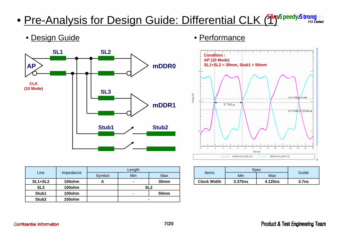
SL1 SL2
SL3
Stub1 Stub2
AP mDDR0
mDDR1
SL2100ohmSL330mm-A100ohmSL1+SL2
-100ohmStub250mm-100ohmStub1
MaxMinSymbolLength
ImpedanceLine
3.7ns4.125ns3.375nsClock WidthMaxMin
GuideSpec
Items
CLK(10 Mode)
Condition : AP (10 Mode)SL1+SL2 = 30mm, Stub1 = 50mm
• Pre-Analysis for Design Guide: Differential CLK (1)• Design Guide • Performance

8/20
Slim/Speedy/StrongPTE Limited
Slim/Speedy/StrongPTE Limited• Pre-Analysis for Design Guide: Differential CLK (2)
• Effect of Length of Stub1 • Effect of Length of Stub2
Length of Stub1 affect pulse width of CLK. Length of Stub2 don’t affect pulse width of CLK.

9/20
Slim/Speedy/StrongPTE Limited
Slim/Speedy/StrongPTE Limited
As the length of stub increase,the level of ripple increase.
• Pre-Analysis for Design Guide: DQS and DQ (Read)• Effect of Stub Length

10/20
Slim/Speedy/StrongPTE Limited
Slim/Speedy/StrongPTE Limited
SL1 SL2
Stub1 Stub2
AP mDDR0
ADDR(01 Mode)
SL2SL3A + 15mm50ohmSL1+SL2
-50ohmStub270mm10mm50ohmStub1
MaxMinSymbolLength
ImpedanceLine
SL3mDDR1
※ To obtain margin for hold time : Length of ADDR > Length of CLK
• Pre-Analysis for Design Guide: ADDR & BA (1)• Design Guide
11/20
Slim/Speedy/StrongPTE Limited
Slim/Speedy/StrongPTE Limited
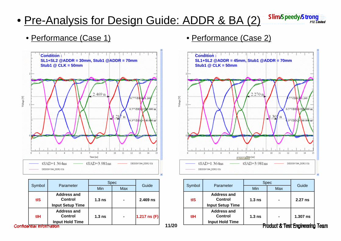
Condition :SL1+SL2 @ADDR = 30mm, Stub1 @ADDR = 70mmStub1 @ CLK = 50mm
Condition :SL1+SL2 @ADDR = 45mm, Stub1 @ADDR = 70mmStub1 @ CLK = 50mm
-
-
MaxSpec
1.217 ns (F)1.3 nsAddress and
ControlInput Hold Time
tIH
2.469 ns1.3 nsAddress and
ControlInput Setup Time
tIS
GuideMin
ParameterSymbol
-
-
MaxSpec
1.307 ns1.3 nsAddress and
ControlInput Hold Time
tIH
2.27 ns1.3 nsAddress and
ControlInput Setup Time
tIS
GuideMin
ParameterSymbol
• Pre-Analysis for Design Guide: ADDR & BA (2)• Performance (Case 1) • Performance (Case 2)

12/20
Slim/Speedy/StrongPTE Limited
Slim/Speedy/StrongPTE Limited
SL1 SL2
Stub1 Stub2
AP mDDR0
CTRL(01 Mode)
SL2SL3A + 40mm50ohmSL1+SL2
-50ohmStub270mm10mm50ohmStub1
MaxMinSymbolLength
ImpedanceLine
SL3mDDR1
※ To obtain margin for hold time :Length of CTRL > Length of CLK -
-
MaxSpec
1.307 ns1.3 nsAddress and
ControlInput Hold Time
tIH
2.359 ns1.3 nsAddress and
ControlInput Setup Time
tIS
GuideMin
ParameterSymbol
• Pre-Analysis for Design Guide: CS, CKE, RAS, CAS & WE
• Design Guide • Performance

13/20
Slim/Speedy/StrongPTE Limited
Slim/Speedy/StrongPTE Limited
SL1
SL2
SL3
Stub1 Stub2
AP
mDDR0
mDDR1CLK(10 Mode)
SL1 SL2
Stub1 Stub2
AP mDDR0mDDR1
DQS / DQ / DM(01 Mode)
SL1
SL2
Stub1 Stub2
AP
mDDR0
ADDR / CTRL(01 Mode)
SL3mDDR1
70mm--50ohmStub2
10mm-50ohmStub1SL2-50ohmSL3
A + 40mm-50ohmSL1+SL2CS / WECKERASCAS
70mm
A + 15mm-50ohmSL1+SL2ADDR
BA
--50ohmStub270mm10mm-50ohmStub1
A-50ohmSL1+SL2DM
--50ohmStub250mm10mm-50ohmStub1
A-50ohmSL1+SL2SL2-50ohmSL1
DQ
30mm-ADiff 100ohmSL1+SL2
CLKSL2-Diff 100ohmSL3
50mm--Diff 100ohmStub1--Diff 100ohmStub2
--50ohmStub250mmSL2-50ohmStub1
A-50ohmSL1+SL2SL2-50ohmSL1
DQS
Pins
10mm-50ohmStub1SL2-50ohmSL3
--50ohmStub2
MaxMinSymbolLength
ImpedanceLine
• Summary of Design Guide for New Test Board

14/20
Slim/Speedy/StrongPTE Limited
Slim/Speedy/StrongPTE Limited
ADDRCTRL(133
Mbps) -1.41 ns-1.300 nstIH3.01 ns--1.300 nstIS@mDDR
(CTRL)
-2.77 ns
MaxMinSpec
@ mDDR(ADDR)
IC
--1.300 nstIS1.53 ns-1.300 nstIH
MaxAnalysis
MinSymbol
CLK@ mDDR1(133 MHz)
CTRL@ mDDR1(133 Mbps)Max Delay
CLK@ mDDR1(133 MHz)
CTRL@ mDDR1(133 Mbps)Min Delay
ADDR@ mDDR1(133 Mbps)Min Delay
ADDR@ mDDR1(133 Mbps)Max Delay
• Analysis of AP-mDDR Interface for Designed PCB : ADDR/CTRL Pins
• Received Pulse @ mDDR : CTRL Pins • Received Pulse @ mDDR : ADDR Pins

15/20
Slim/Speedy/StrongPTE Limited
Slim/Speedy/StrongPTE Limited
1.91 ns1.68 ns-1.500 nstDSH1.71 ns1.95 ns-1.500 nstDSS5.57 ns
-Spec In
---
MaxMin
1.61 ns-0.800 nstDH1.85 ns-0.800 nstDS
5.48 ns-1.875 nstWPREH--0.000 nstWPRES
Spec In9.375 ns5.625 nstDQSS
@ mDDR
--1.300 nstWPREH--1.300 nstWPRES-9.375 ns9.142 nstDQSS
@ AP(01 Mode)
SpecIC
MaxAnalysis
MinSymbol
CLK(133MHz)
DQS(133MHz)
DQ(266
Mbps)
DQ(266
Mbps)
CLK @ mDDR0(133 MHz)
DQS0/1 @ mDDR0(133 MHz)
CLK @ mDDR1(133 MHz)
DQS2/3 @ mDDR0(133 MHz)
MinDelay
MaxDelay
DQS @ mDDR0(133 MHz)
DQ @ mDDR0(266 Mbps)
DQS @ mDDR1(133 MHz)
DQ @ mDDR1(266 Mbps)
• Analysis of AP-mDDR Interface for Designed PCB : Write Mode• Received Pulse @ mDDR : CLK-DQS
• Received Pulse @ mDDR : DQS-DQ

16/20
Slim/Speedy/StrongPTE Limited
Slim/Speedy/StrongPTE Limited
DQS(133MHz)
DQ(266
Mbps)
0.45 ns0.5 ns-tDDS@ AP--0 nstDQSQ@ mDDR
SpecIC
MaxAnalysis
MinSymbol
• Analysis of AP-mDDR Interface for Designed PCB : Read Mode• Received Pulse @ AP : DQS-DQ
Design Guide에따른 Design이 Spec을만족함 Design Revision 제거

17/20
Slim/Speedy/StrongPTE Limited
Slim/Speedy/StrongPTE Limited
VDD_INT are designed according to our guide.The impedance of VDD_INT are small according to our expectation.
~350MHz @1ohm
• Analysis of Power Impedance for VDD_INT
• Layout • Results

18/20
Slim/Speedy/StrongPTE Limited
Slim/Speedy/StrongPTE Limited
~110MHz @1ohm
VDD_ARM are not designed according to our guide.The impedance of VDD_ARM are larger than those of VDD_INT.The layout for VDD_ARM need improvement.
• Analysis of Power Impedance for VDD_ARM
• Layout • Results

19/20
Slim/Speedy/StrongPTE Limited
Slim/Speedy/StrongPTE Limited
Increase of area
Decrease ofdistance to GND
110 MHz 240 MHz 310 MHz 410 MHz
Increase of areaDecrease
ofdistanceto GND
Addition ofdecouplingcapacitor(10uFx2)
• Improvement of Power Impedance for VDD_ARM• Layout Modification
20/20
Slim/Speedy/StrongPTE Limited
Slim/Speedy/StrongPTE Limited• Conclusion
Pre-Analysis를사용한 Design Guide 수립및적용으로 Design Revision없이특성확보FPGA Path에의한 Stub 영향을사전에고려가능Design 편의성고려한 Guide 수립 : 허용가능한 Trace 길이 Guide
PCB 제작전의 Power Impedance 분석으로 Design 최적화수행