design for excellence (dfx) - generis · pdf filedesign for excellence (dfx) brian morrison,...
TRANSCRIPT

Design for Excellence (DFX)
Brian Morrison, B.A.Sc., P. Eng. Director, Value Engineering & Technology Oct 5, 2016
Driving Product Optimization Through Early Stage Supplier Engagement
2Strictly Confidential [Rev. July 2015]
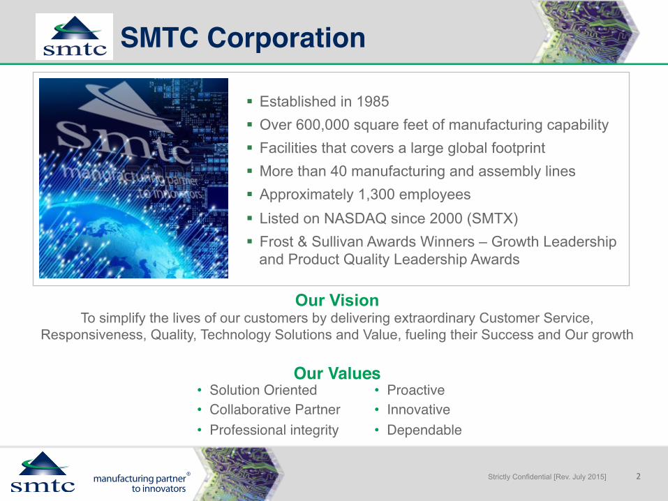
SMTC Corporation
§ Established in 1985 § Over 600,000 square feet of manufacturing capability § Facilities that covers a large global footprint § More than 40 manufacturing and assembly lines § Approximately 1,300 employees § Listed on NASDAQ since 2000 (SMTX) § Frost & Sullivan Awards Winners – Growth Leadership
and Product Quality Leadership Awards
Our Vision To simplify the lives of our customers by delivering extraordinary Customer Service,
Responsiveness, Quality, Technology Solutions and Value, fueling their Success and Our growth
Our Values• Solution Oriented• Collaborative Partner• Professional integrity
• Proactive• Innovative• Dependable

3Strictly Confidential [Rev. July 2015]
Medical Device Markets
Specialists in the Design and Manufacture of Complex Class I and II Medical Devices We design and manufacture class I and II medical devices that require a mix of highly specialized technologies including: • Diagnostic devices • Imaging equipment • laboratory equipment • Patient Monitoring systems • Infusion Pumps • Dispensing Systems • Consumer Wellness Products.

4Strictly Confidential [Rev. July 2015]
DFX Product Optimization
§ What is DFX? § DFX Benefits § Value Equation § Product Design Review § Ability to Impact Product Value § Early Supplier Involvement (ESI) § Impact of Design Decisions § Applying DfX to Product Development
5Strictly Confidential [Rev. July 2015]
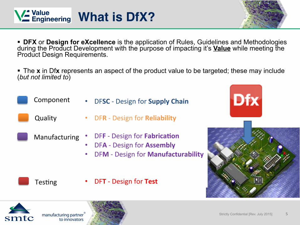
What is DfX?
§ DFX or Design for eXcellence is the application of Rules, Guidelines and Methodologies during the Product Development with the purpose of impacting it’s Value while meeting the Product Design Requirements. § The x in Dfx represents an aspect of the product value to be targeted; these may include (but not limited to)
Component
Quality
Manufacturing
Tes:ng
• DFSC -‐ Design for Supply Chain
• DFR -‐ Design for Reliability
• DFF -‐ Design for Fabrica3on • DFA -‐ Design for Assembly • DFM -‐ Design for Manufacturability
• DFT -‐ Design for Test

6Strictly Confidential [Rev. July 2015]
Product Value Equation
Performance can be a function, need, feature or aspect that is deemed
critical to the product design.
Cost can include material, labor, test, logistics or any other aspect required to provide the required performance.
Quality
Features
Reliability
Life:me Func:on
Components
Design
Labor
Tes:ng PCB

7Strictly Confidential [Rev. July 2015]
Typical Product Development
Requirements Feasibility Design Input/Specifica:on Design Phase Verifica:on/
Valida:on Cer:fica:on
What does the product need to do?
Can the technology support the need? Gaps, Risk, Unknowns.
What will the product be able to do?
What will the product look like, how will it func:on, how much will it cost?
Does the product perform as expected?
Does the product meet the regulatory requirements?
DfX Review
DfX Review
DfX Review
DfX Review
DfX Review

8Strictly Confidential [Rev. July 2015]
DFX Benefits
§ Ease of Manufacturing § Improved PCB yield, performance and cost (DFF) § Improved Assembly yield and reduced labour content (DFA)
§ Optimized Test Strategy § Improved Coverage, Reliability and Final yield, reduced RMA and field failures.
(DFT, DFR) § Reduced development engineering resource commitment, improved time to market
§ Product/ Process Stability and Repeatability § Reduced lead time, improved availability/lifecycle and material costs (DFSC) § High quality, reliable and robust performance for the life of the product (DFR)
§ Capability § Improved Production Stability and Predictability (DFM)
§ First Pass Yield and Capacity § Continuous Improvement (DFM)

9Strictly Confidential [Rev. July 2015]
Ability to Impact Product Value
• Component selection – Major (e.g. Processor)
• Hardware / Software partitioning
• Schematic Design • ASIC/FPGA Design • Component
Selection
• PCB Layout • DFM • DFT • Component
Selection (e.g. passives)
• Quick Turn Prototype
• Early DFM/DFT Feedback
• Device level testing • System integration
testing • EMC testing • Agency submissions
• Supply chain tweaking
• Continuous process improvement
AB
ILIT
Y TO
IMPA
CT
TIMELINE
DFSC – Design For Supply Chain
DFT – Design For Test
DFA – Design for Assembly
DFM – Design for Manufacturability
DFR – Design For Reliability
Architecture High Level Design Physical Design Prototype Valida3on NPI Volume
80% of Product’s Recurring Cost Established
DFA – Design for Assembly DFF – Design for Fabrication
TYPICAL PRODUCT DEVELOPMENT CYCLE
DFX
EN
GA
GEM
ENT
CO
STED
AC
TIVI
TIES
10Strictly Confidential [Rev. July 2015]
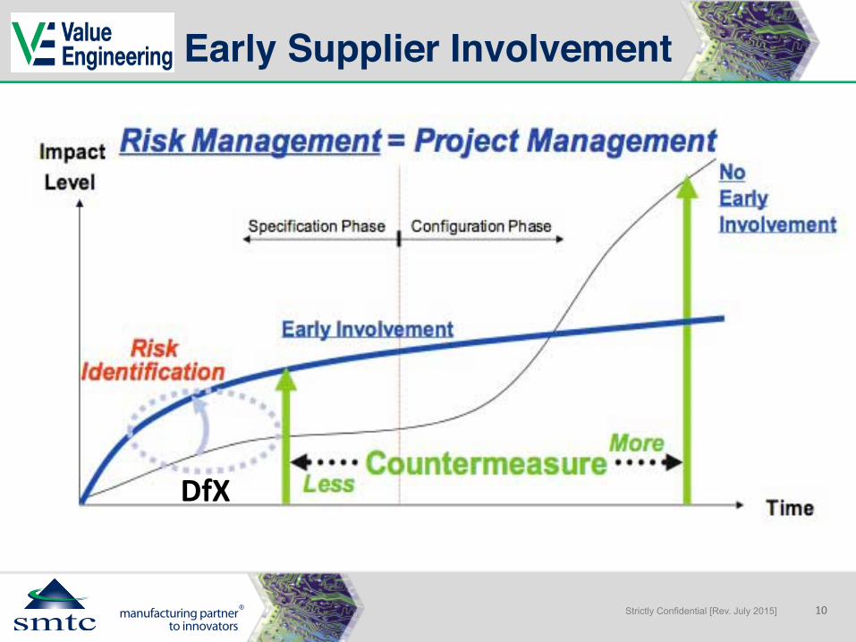
Early Supplier Involvement
DfX

11Strictly Confidential [Rev. July 2015]
§ Selection of Critical Components
§ Defining Environmental Requirements
§ Detailed Product Specifications
§ Hardware / Software Requirements
§ Defining Key Features/ Functions
Architecture High Level Design
Physical Design Prototype Valida3on NPI Volume
Impact of Design Decisions
§ Design for Reliability (DFR) § Critical Component Selection § Desired Lifetime/ Environment § PCB Design Considerations
§ Design for Supply Chain (DFSC) § Predicted Lifecycle and
Sourcing § Process Compatibility § Strategic Supplier Alignment
Impact of Architecture Design Decisions

12Strictly Confidential [Rev. July 2015]
Design for Reliability (DFR) Total Cost of Ownership à Cost vs. Reliability
Critical Component Considerations § Physics of Failure § Mean Time to Failure § Technology § Wear Out
Environmental Considerations
§ Temperature – Operating/ Max § Exposure - Humidity § Stress - Electrical Load/ Vibration/ Shock/
Power Cycling PCB Design
§ Materials - Surface Finish. Laminate § Technology - Blind/Buried Vias, Microfill/ Plating § Electrical Clearance
13Strictly Confidential [Rev. July 2015]
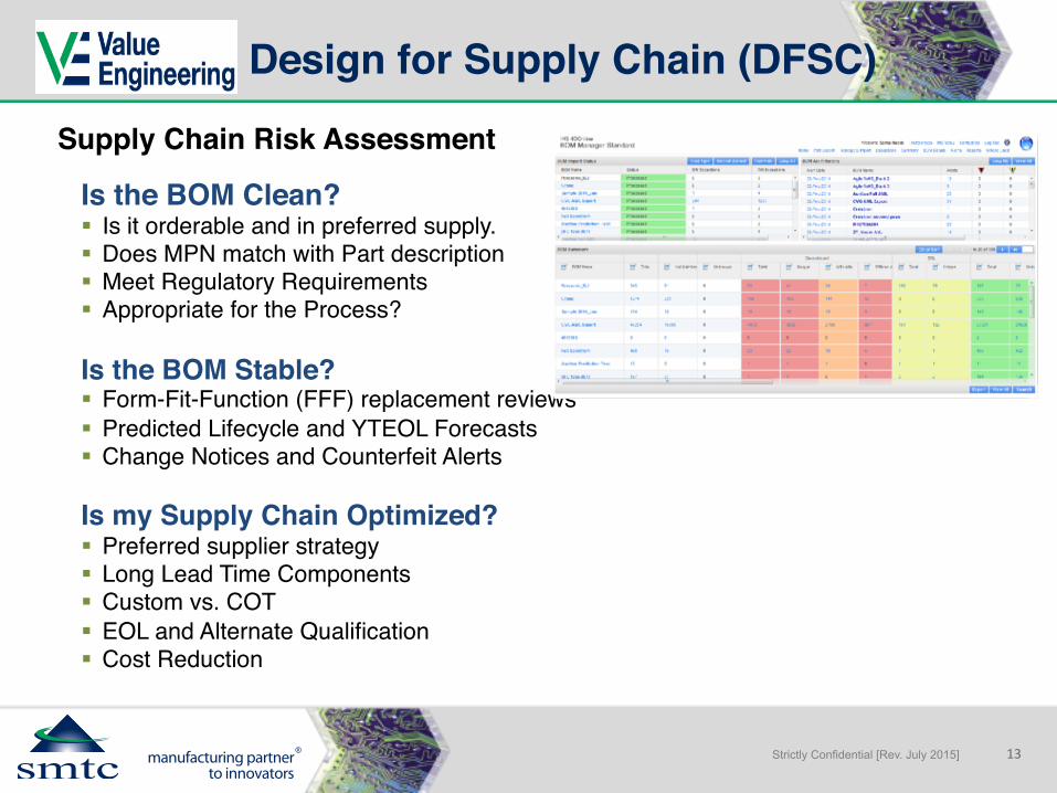
Design for Supply Chain (DFSC)
Is the BOM Clean? § Is it orderable and in preferred supply.§ Does MPN match with Part description§ Meet Regulatory Requirements§ Appropriate for the Process?
Is the BOM Stable? § Form-Fit-Function (FFF) replacement reviews§ Predicted Lifecycle and YTEOL Forecasts§ Change Notices and Counterfeit Alerts
Is my Supply Chain Optimized? § Preferred supplier strategy§ Long Lead Time Components§ Custom vs. COT§ EOL and Alternate Qualification§ Cost Reduction
Supply Chain Risk Assessment

14Strictly Confidential [Rev. July 2015]
BOM Health Check
§ Supply Chain Scorecard
§ Approved Manufacturer List (AML) § Total AML: 7883 § Total Active AML: 5093
§ Risk: § Discontinued w/o Alts: 142 § Discontinued with Alts: 498 § EOL: 26 § Single Sourced 1860 § RoHS Non-Compliant 87
§ Calculated Health Score: § 612.6 out of a possible 1000

15Strictly Confidential [Rev. July 2015]
BOM Analysis
Risks Identified § Discontinued AML § Years to EOL (YTEOL) – Lifecycle § Non-compliant - Regulatory § Single Sourced AML
Risk Mitigation § Evaluate FFF replacement recommendations or
develop strategy to address Discontinued/EOL components.
§ Qualify RoHS equivalent orderable part numbers or provide alternates to address compliancy issues
§ Continuity of supply through strategic FFF AML Alternates to provide multiple sources to single sourced components.
§ Re-design requirements and NPI funnel.

16Strictly Confidential [Rev. July 2015]
DFSC Case Study
Strategic Supply Chain Alignment Project A Scope of the Project Targeting cost reduction, and obsolesce 40 parts were identified as FFF alternates to existing approved AML with a potential for 20% reduction in material costs. Cost avoidance of $38K was identified through alternate sourcing due to obsolesce
Value Engineering Services Implemented Cost Savings § Component Engineering § $126K
Alternate Vendors Project B Scope of the Project FFF alternate to address poor supplier performance on a Power Supply resulting in 8% reduction in cost. Full functional part evaluation in system and test reports provided to support qualification
Value Engineering Services Implemented Cost Savings § Component Engineering § $87K

17Strictly Confidential [Rev. July 2015]
Impact of High Level Design Decisions
§ Design for Testability § Schema:c Review § Test Strategy Review
§ Design for Supply Chain (DFSC) § Predicted Lifecycle and Sourcing § Process Compa:bility § Strategic Supplier Alignment
Architecture High Level Design
Physical Design Prototype Valida3on NPI Volume
• Schema3c Design
• ASIC/ FBGA Design
• Cont’d Component Selec3on
• Hardware/ SoQware Requirements
• Defining Key Func3ons/ Features
• Test and Performance Defini3on
Impact of Design Decisions
18Strictly Confidential [Rev. July 2015]
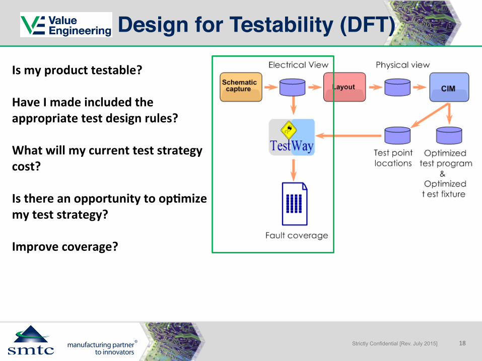
Design for Testability (DFT)
Is my product testable? Have I made included the appropriate test design rules?
What will my current test strategy cost?
Is there an opportunity to op3mize my test strategy? Improve coverage?

19Strictly Confidential [Rev. July 2015]
Impact of Physical Design Decisions
§ Impact of Design Decisions
§ PCB Layout and Routing
§ PCB Stackup and Fabrication
§ Physical Placement § Via – Blind. Buried § Test Point § Access
§ Design for Assembly (DFA) § Physical Layout § Assembly and Manufacturer
§ Design for Fabrication (DFF) § Stack up and Impedance § PCB Fabrication Design Rules
§ Design for Testability (DFT) § Nodal Analysis § Test Strategy Development
Architecture High Level Design
Physical Design Prototype Valida3on NPI Volume

20Strictly Confidential [Rev. July 2015]
Physical Design Review Timing
Pre-‐plac ement P lacement
Manufac turingpre-‐build review
(Pre-‐DFM)
AssemblyAnalys is
(Pre-‐DFA)
Assembly Analys is(DFA)
PCB Fabric ationAnalys is
(DFF)Test Ac c ess
Analys is(DFT)
IC T PressureAnalys is
(FEA)
Manufac turingpost build review
(Post-‐DFM)
Gerberrelease
# daysTBD
Week 2S tart Week 4 Week 6 Week 8 Week 10 Week 12
# daysTBD
5 days
90% routingcompletion of tight
sec tions
Plac ementfreeze
Prototypeshipment
BOMAnalys is
Routing Verific ation PCB FAB PC BA produc tion
Typical Engagement Target Engagement Too late to impact
change

21Strictly Confidential [Rev. July 2015]
Design for Assembly (DFA)
Component models can be used to replicate a virtual prototype.
Utilizing Valor or similar software, design rules checks can be made to generate a manufacturing risk assessment report.
§ Component Analysis§ Pad stack Analysis§ Pin to Pad Analysis§ Test Point Analysis § Solder Paste Analysis

22Strictly Confidential [Rev. July 2015]
Design for Assembly (DFA)
Example DFA Output outlining Critical (Major), Hot (Yield improvement), Warm (Minor), Cool (No immediate concern) and Ignore (acceptable)

23Strictly Confidential [Rev. July 2015]
Design for Reliability (DFR)Ref Des U37, U38, distance between pad too close (0.0059”). Prone to solder bridge. Recommend decreasing pad from 13.78 mil to 11 mils.
Quality and Reliability Concern. 28 OFE, 14 Location – 392 OpportunitiesProbability of Occurrence 40%Expected Yield Detractor 0.72%Rework Cost $0.42Potential Failure Cost $727.50
Ref R1050, C239, RN96, FB2, etc., masked trace between toe print is too thin, may break and cause insufficient solder. Minimum recommended clearance between exposed via and toeprint is 5mil.
Quality and Reliability Concern. 2 OFE, 130 Locations – 260 OpportunitiesProbability of Occurrence 50%Expected Yield Detractor 2.5%Rework Cost $2.80Potential Failure Cost $4,021.01
Ref Des U48, U103, land pattern is not optimal, heel distance is too big. Too much heel may cause solder bridge under component, not visible to visual inspection. Recommended to decrease by 25 mil on heel side.
Quality and Reliability Concern. 50 OFE, 2 Location – 100 OpportunitiesProbability of Occurrence 50%Expected Yield Detractor 0.23%Rework Cost $0.70Potential Failure Cost $386.63

24Strictly Confidential [Rev. July 2015]
Design for Fabrication (DFF)
What stackup do I need for my impedance requirements? Trace width? § Reviews typically include determining workable stackups, including
impedance trace width
Is my design within the capability of my fab house? Do I have special requirements/ features? • Most supplier utilize automated DFX tools
such as Valor to apply their internal Design Rule Checks (DRC) and will provide comprehensive DFM reports for Design Reviews

25Strictly Confidential [Rev. July 2015]
Design for Fabrication (DFF)
• Suppliers will typically provide their DFM guidelines upon request.
• Incorporating these rules into your native Design Package can help drive value further up the Product Development Cycle

26Strictly Confidential [Rev. July 2015]
What is the op3mal Panel Design § U:liza:on of a master panel is a
primary cost driver.
§ Fabricator will focus on high u:liza:on without considera:on for assembly
• Manufacturer will focus on ease of assembly without considera:on for u:liza:on
Op:mal panel is one that considers both!
Design for Fabrication (DFF)

27Strictly Confidential [Rev. July 2015]
DFF Case Study
Panel Optimization Project A Scope of the Project Optimized panel design to meet automated equipment requirements based on EAU increased the master panel utilization from 52% to 72% yielding 20% more panels than the existing design and providing high throughput and lower cost per unit.
Value Engineering Services Implemented Cost Savings § PCB Panel Design § $20K
Material Specification Project B Scope of the Project Relax Tg constraints for 10 layer board and realize savings by switch from S1000-2 (Tg 170) to IT158 (Tg 150) with existing supplier
Value Engineering Services Implemented Cost Savings § Design for Fabrication § $34K

28Strictly Confidential [Rev. July 2015]
Design for Testability (DFT)Do I have the necessary access to support my coverage needs? Are my test points appropriate for my test strategy? What is my product coverage? What is not tested? Is my test plan still valid?

29Strictly Confidential [Rev. July 2015]
Test Strategy Overview
Electrical Tes3ng $$ • Is the component measurement correct? • Strategies include Manufacturing Defect Analyzer (MDA) Flying Probe,
Structural Tes3ng $ • Is the component soldered, present and correct? • Strategies include Visual Inspec:on, X-‐Ray (2D or 3D) and Automated Op:cal Inspec:on (AOI)
Func3onal Tes3ng $$$ • Does the product func:on as expected? • Strategies include In-‐Circuit Test (ICT) and Func:onal Test (FT)
Reliability Tes3ng $$$ • Does my product perform in the intended environment? • Strategies include Run-‐in, Burn-‐in and Environmental Stress Screening (ESS)

30Strictly Confidential [Rev. July 2015]
Test Strategy Analysis
OPTIMAL

31Strictly Confidential [Rev. July 2015]
DFT Case Study
Test Strategy Recommendation Project A
Scope of the Project
Review existing test strategy and coverage to determine optimal test strategy to provide highest first pass yield, lowest coverage gaps, RMA and overall cost of quality.
Value Engineering Services Implemented Potential Savings
§ Design for Test– Recommend AOI and ICT (FCT only required if full analog frequency testing required) over existing AOI and 5DX testing (no electrical). Reduce coverage gaps from 0.24% to 0.04% and expected RMA from 11.38% to 3.94%. ROI 0.20 years.
§ ICT Development – Quote includes all aspects of ICT development, including future maintenance and production support.
§ $89K - $18K = $61K

32Strictly Confidential [Rev. July 2015]
Impact of Prototype Design Decisions
• Quick Turn vs. Production Supplier?
• Production Tooling or Soft Tool?
• Material and Component Sourcing Tradeoffs?
• Understanding your supply Risk, Process Gaps and Plan for them.
Architecture High Level Design
Physical Design Prototype Valida3on NPI Volume
§ Design for Manufacturability (DFM)
§ Equipment Requirements § Tooling Considerations § Process Considerations § Labor Requirements

33Strictly Confidential [Rev. July 2015]
Design for Manufacturing (DFM)
What compromises were made during prototype vs. produc3on?
§ Do I understand the tolerances and gaps between suppliers?
§ What is my transfer plan, knowledge plan?
§ Manage Variability and Risk

34Strictly Confidential [Rev. July 2015]
Design for Manufacturing and Assembly
Is my product design op3mized for cost?
DFMA Simplifica3on • Minimize Opera:ons • Minimize Weight • Simplify Assembly • Tooling Complexity
Supplier Levers • Reduced Tooling Costs • Reduced Labor Cost • Minimal Equipment Needs • Op:mize Piece Price

35Strictly Confidential [Rev. July 2015]
Impact of Validation Design Decisions
§ Design Verification Testing (DVT) § Highly Accelerated Life Test (HALT) § Highly Accelerated Stress Screen (HASS)
• What is my product requirements?
• Is my plan representative of the product end user environment?
• Is my test coverage effective to detect failures to drive corrective action?
Architecture High Level Design
Physical Design Prototype Valida3on NPI Volume

36Strictly Confidential [Rev. July 2015]
§ What is the right test plan?
• Design Verifica3on Test • U:lizes rela:vely low stresses and requires many cycles. Typical user environment.
• Design Vibra3on, Drop and Impact • Replicate Product Stresses
• Design Highly Accelerated Life Test (HALT) • Run at the edge of the opera:ng limits over :me to emulate typical product life:me.
• Design Highly Accelerated Stress Screen (HASS) • Test methods specifically designed on finding defects in products, destruc:ve limit.
Design for Reliability (DFR)

37Strictly Confidential [Rev. July 2015]
Impact of NPI Design Decisions
Volume Production Supplier Selection Transfer/ Mitigation Plan Critical Component and Risk Management, Supply Chain risks?
Introduction of Production Tooling/ Process. Master Device Plan Development and Qualification
Architecture High Level Design
Physical Design Prototype Valida3on NPI Volume
§ Design for Manufacturability (DFM) § First Article Reports § Process Development (pFMEA) § Yield and Detractor Analysis § Problematic Design Improvements
§ Design for Testability (DFT) § Coverage Gap Strategy
38Strictly Confidential [Rev. July 2015]
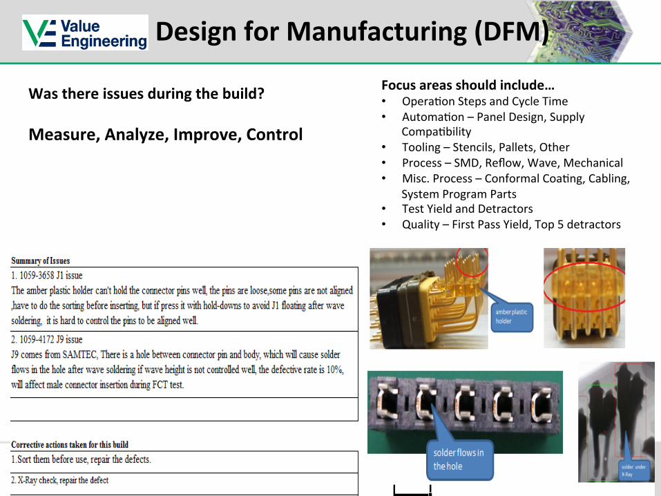
Was there issues during the build? Measure, Analyze, Improve, Control
Focus areas should include… • Opera:on Steps and Cycle Time • Automa:on – Panel Design, Supply
Compa:bility • Tooling – Stencils, Pallets, Other • Process – SMD, Reflow, Wave, Mechanical • Misc. Process – Conformal Coa:ng, Cabling,
System Program Parts • Test Yield and Detractors • Quality – First Pass Yield, Top 5 detractors
Design for Manufacturing (DFM)

39Strictly Confidential [Rev. July 2015]
Impact of Volume Production Decisions
What are the key DfX considera3ons to ensure a successful product ramp to volume? 1) Product Design for Manufacturability (DFM Gaps addressed)
• Even small defects can become big problems at volume.
• Focus on ability for full automa3on, minimal touchup/repair and repeatability of manufacturing.
2) Product Design for Testability (DFT Coverage Gaps addressed)
• Does the Test plan s3ll make sense?
• Detec3on should be as early as possible in the process to have an impact.
.
Architecture High Level Design
Physical Design Prototype Valida3on NPI Volume

40Strictly Confidential [Rev. July 2015]
Impact of Volume Production Decisions
What key A`ributes of a volume supplier should be reviewed? 3) Product/ Process Stability and Repeatability -‐ Tooling
4) Capability -‐ Equipment, Repair, Processes, Troubleshoot
5) First Pass Yield and Capacity
Architecture High Level Design
Physical Design Prototype Valida3on NPI Volume

41Strictly Confidential [Rev. July 2015]
§ Performance vs. Cost trade-offs should never lose sight of requirements.
§ DfX is a design review tool to help align requirements
§ Collaboration is key to a successful DfX implementation program
§ Early detection and supplier involvement helps identify risk for an effective program management
Final Words

42Strictly Confidential [Rev. July 2015]
THANK YOUSMTC Corporation