design example report - ac-dc converters · design example report title 24 w high efficiency...
TRANSCRIPT
Power Integrations 5245 Hellyer Avenue, San Jose, CA 95138 USA.
Tel: +1 408 414 9200 Fax: +1 408 414 9201 www.power.com
Design Example Report
Title 24 W High Efficiency Adaptor Using LinkSwitchTM-HP LNK6775E and Synchronous Rectifier
Specification 90 VAC – 265 VAC Input; 12 V, 2 A Output
Application Adapter
Author Applications Engineering Department
Document Number DER-416
Date July 17, 2017
Revision 1.5
Summary and Features Small PCB size of 84.1 mm x 44.4 mm Very low no-load input power (84 mW / 12 V at 230 VAC) High average efficiency at 115/230 VAC / 60 Hz (87.46%)
Exceeds Energy Star 2.0 Efficiency Requirements: >82.9% at 115 V / 60 Hz, and230 V / 50 Hz, with very high efficiency in both standby and sleep modes
Exceeds USA Energy Independence and Security Act 2007 of 86.2% Exceeds the latest EU CoC v5 and EuP Tier 2 requirement of 86.8% 80.6% efficiency at 230 VAC 10% load
Excellent transient load response Latch for thermal shutdown and overvoltage protection, and auto restart for lost regulation
PATENT INFORMATION The products and applications illustrated herein (including transformer construction and circuits external to the products) may be covered by one or more U.S. and foreign patents, or potentially by pending U.S. and foreign patent applications assigned to Power Integrations. A complete list of Power Integrations' patents may be found at www.powerint.com. Power Integrations grants its customers a license under certain patent rights as set forth at <http://www.powerint.com/ip.htm>.
DER-416 24 W Adaptor with LinkSwitch-HP and SR 17-Jul-17
Page 2 of 51
Power Integrations, Inc. Tel: +1 408 414 9200 Fax: +1 408 414 9201 www.power.com
Table of Contents 1 Introduction ................................................................................................................ 4 2 Power Supply Specification ......................................................................................... 6 3 Schematic ................................................................................................................... 7 4 Circuit Description ...................................................................................................... 8
4.1 Input Rectification and Filtering ........................................................................... 8 4.2 LinkSwitch-HP Primary ......................................................................................... 8 4.3 Primary RZCD Clamp ........................................................................................... 8 4.4 Synchronous Rectification and Controller ............................................................ 9 4.5 External Current Limit Setting .............................................................................. 9 4.6 Feedback and Compensation Network ................................................................. 9
5 PCB Layout ............................................................................................................... 11 6 Bill of Materials ......................................................................................................... 12 7 Transformer Specification (T1) ................................................................................. 14
7.1 Electrical Diagram .............................................................................................. 14 7.2 Electrical Specifications ...................................................................................... 14 7.3 Material List ....................................................................................................... 14 7.4 Build Diagram .................................................................................................... 15 7.5 Winding Instructions .......................................................................................... 16 7.6 Winding Illustrations .......................................................................................... 17
8 Input Common Mode Choke Specification (L4) ......................................................... 22 8.1 Electrical Diagram .............................................................................................. 22 8.2 Electrical Specifications ...................................................................................... 22 8.3 Material List ....................................................................................................... 22 8.4 Winding Instructions .......................................................................................... 22 8.5 Illustrations ........................................................................................................ 22
9 Output Common Mode Choke Specification (L5) ...................................................... 23 9.1 Electrical Diagram .............................................................................................. 23 9.2 Electrical Specifications ...................................................................................... 23 9.3 Materials ............................................................................................................ 23 9.4 Winding Instructions .......................................................................................... 23 9.5 Illustrations ........................................................................................................ 23
10 Transformer Design Spreadsheet .......................................................................... 24 11 eSIP Heat Sink Assemblies .................................................................................... 26
11.1 Heat Sink Fabrication Drawing ........................................................................... 26 11.2 Heat Sink Assembly Drawing ............................................................................. 27 11.3 eSIP and Heat Sink Assembly Drawing .............................................................. 28
12 Performance Data ................................................................................................. 29 12.1 Full Load Efficiency ............................................................................................ 29 12.2 Active Mode Efficiency ....................................................................................... 30 12.3 Energy Efficiency Requirements ......................................................................... 32
12.3.1 Energy Efficiency Requirement Table ......................................................... 33 12.3.2 USA Energy Independence and Security Act 2007 ..................................... 34

17-Jul-17 DER-416 24 W Adaptor with LinkSwitch-HP and SR
Page 3 of 51
Power Integrations Tel: +1 408 414 9200 Fax: +1 408 414 9201
www.power.com
12.3.3 ENERGY STAR EPS Version 2.0 ................................................................... 34 12.4 No-Load Input Power ......................................................................................... 35 12.5 Regulation .......................................................................................................... 36
12.5.1 Line Regulation at Full Load ........................................................................ 36 12.5.2 Load Regulation .......................................................................................... 37
13 Thermal Performance ............................................................................................ 39 14 Waveforms ............................................................................................................ 40
14.1 Drain Voltage and Current, Normal Operation ................................................... 40 14.2 Output Voltage Start-up Profile .......................................................................... 40 14.3 Drain Voltage and Current Start-up Profile ........................................................ 41 14.4 Voltage Stress of Secondary SR ......................................................................... 42 14.5 Load Transient Response, 0.2 A – 2 A – 0.2 A Load Step .................................. 43 14.6 Output Ripple Measurements ............................................................................. 44
14.6.1 Ripple Measurement Technique .................................................................. 44 14.6.2 Measurement Results At The End of Cable ................................................. 45
15 AC Surge (Resistive Full Load at the Output) ........................................................ 46 16 Conducted EMI ...................................................................................................... 47 17 Revision History ..................................................................................................... 50 Important Note: Although this board is designed to satisfy safety isolation requirements, the engineering prototype has not been agency approved. Therefore, all testing should be performed using an isolation transformer to provide the AC input to the prototype board.
DER-416 24 W Adaptor with LinkSwitch-HP and SR 17-Jul-17
Page 4 of 51
Power Integrations, Inc. Tel: +1 408 414 9200 Fax: +1 408 414 9201 www.power.com
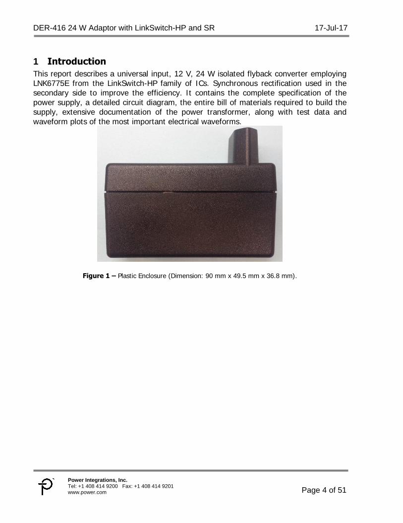
1 Introduction This report describes a universal input, 12 V, 24 W isolated flyback converter employing LNK6775E from the LinkSwitch-HP family of ICs. Synchronous rectification used in the secondary side to improve the efficiency. It contains the complete specification of the power supply, a detailed circuit diagram, the entire bill of materials required to build the supply, extensive documentation of the power transformer, along with test data and waveform plots of the most important electrical waveforms.
Figure 1 – Plastic Enclosure (Dimension: 90 mm x 49.5 mm x 36.8 mm).
17-Jul-17 DER-416 24 W Adaptor with LinkSwitch-HP and SR
Page 5 of 51
Power Integrations Tel: +1 408 414 9200 Fax: +1 408 414 9201
www.power.com
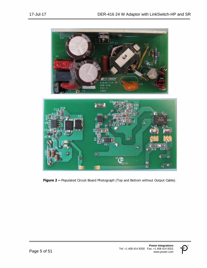
Figure 2 – Populated Circuit Board Photograph (Top and Bottom without Output Cable).
DER-416 24 W Adaptor with LinkSwitch-HP and SR 17-Jul-17
Page 6 of 51
Power Integrations, Inc. Tel: +1 408 414 9200 Fax: +1 408 414 9201 www.power.com
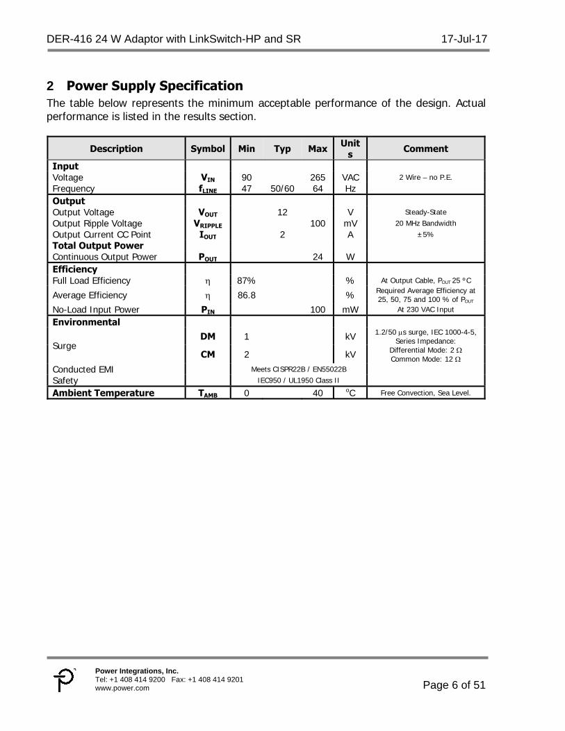
2 Power Supply Specification The table below represents the minimum acceptable performance of the design. Actual performance is listed in the results section.
Description Symbol Min Typ Max Units Comment
Input Voltage VIN 90 265 VAC 2 Wire – no P.E.
Frequency fLINE 47 50/60 64 Hz
Output
Output Voltage VOUT 12 V Steady-State
Output Ripple Voltage VRIPPLE 100 mV 20 MHz Bandwidth
Output Current CC Point IOUT 2 A ±5%
Total Output Power
Continuous Output Power POUT 24 W
Efficiency
Full Load Efficiency 87% % At Output Cable, POUT 25 ºC
Average Efficiency 86.8 % Required Average Efficiency at 25, 50, 75 and 100 % of POUT
No-Load Input Power PIN 100 mW At 230 VAC Input
Environmental
Surge DM 1 kV 1.2/50 s surge, IEC 1000-4-5,
Series Impedance: Differential Mode: 2 Common Mode: 12 CM 2 kV
Conducted EMI Meets CISPR22B / EN55022B
Safety IEC950 / UL1950 Class II
Ambient Temperature TAMB 0 40 oC Free Convection, Sea Level.
17-Jul-17 DER-416 24 W Adaptor with LinkSwitch-HP and SR
Page 7 of 51
Power Integrations Tel: +1 408 414 9200 Fax: +1 408 414 9201
www.power.com
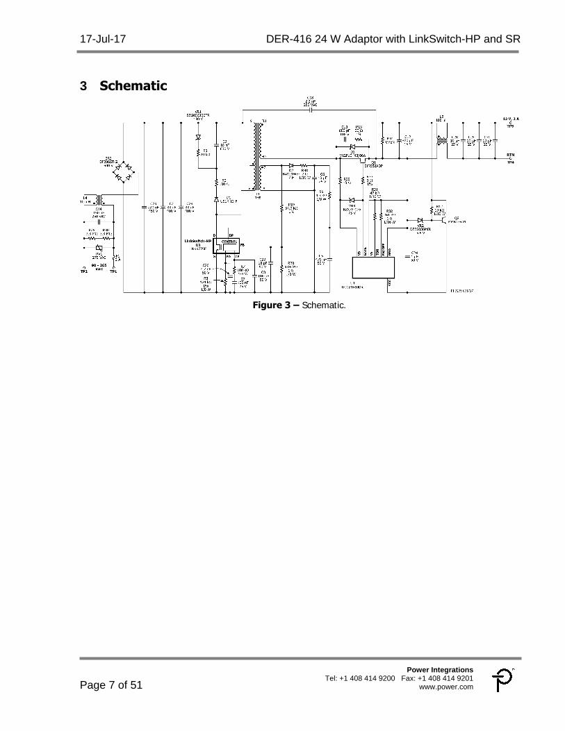
3 Schematic
Figure 3 – Schematic.
DER-416 24 W Adaptor with LinkSwitch-HP and SR 17-Jul-17
Page 8 of 51 Power Integrations, Inc. Tel: +1 408 414 9200 Fax: +1 408 414 9201 www.power.com
4 Circuit Description
4.1 Input Rectification and Filtering
Bridge rectifier BR2 rectifies the AC input which is filtered by C2, C25 and C26. Inductor L4, C14 together C2, C25 and C26 are used to attenuate differential mode and common mode conducted EMI. Shielding techniques were used in the construction of transformer T1 to reduce common mode EMI displacement currents. This filter arrangement, the shield techniques together with the IC’s frequency jitter function provide excellent EMI performance for this solution with a Y capacitor and a primary-side RZCD clamp circuit.
4.2 LinkSwitch-HP Primary The LNK6775E device (U3) integrates an oscillator, an error amplifier and multi-mode control circuit, start-up and protection circuitry and a high-voltage power MOSFET all in one monolithic IC.
One side of the power transformer is connected to the high-voltage bus and the other side is connected to the DRAIN (D) pin of U3. At the start of a switching cycle, the controller turns the power MOSFET on and current ramps up in the primary winding, which stores energy in the core of the transformer. When that current reaches the limit threshold which is set by the output of internal error amplifier COMPENSATION (CP) pin voltage), the controller turns the power MOSFET off. Due to the phasing of the transformer windings and the orientation of the output diode, the stored energy then induces a voltage across the secondary winding, which forward biases the output diode, and the stored energy is delivered to the output capacitor.
Capacitor C5 (0.47 F) connected to the BYPASS (BP) pin sets overvoltage protection (OVP) and over-temperature protection (OTP) to latching and lost regulation protection to automatic restart attempts (auto-restart) after a given off-period (typ. 1500 ms).
4.3 Primary RZCD Clamp Diode D1, VR1, C3, R2 and R3 form a RZCD snubber that is used to limit the voltage stress across the LinkSwitch-HP. Peak drain voltage is therefore limited to typically less than 580 V at 265 VAC – providing significant margin to the 725 V drain voltage (BVDSS). Zener diode VR1 prevents the capacitor C3 from fully discharging every switching cycle to reduce power consumption during standby operation.
Diode D1, R2, VR1, C3, R5 and R6 form a RCD snubber that is used to limit the voltage stress across the LinkSwitch-HP. Peak drain voltage is therefore limited to typically less than 580 V at 265 VAC – providing significant margin to the 725 V drain voltage (BVDSS).
A fast diode is needed for both snubber diode D1 and diode rectifier of bias winding D2. During our test, we found SR could be turned on unexpectedly by DCM ring if slow diode
17-Jul-17 DER-416 24 W Adaptor with LinkSwitch-HP and SR
Page 9 of 51
Power Integrations Tel: +1 408 414 9200 Fax: +1 408 414 9201
www.power.com
were used for the bias diode. This unexpected SR turning on results in reverse current, and both the SR driver and SR itself can be blown up. For all line and load conditions, the voltage stress and gate driving of SR need to be checked carefully to avoid this problem.
4.4 Synchronous Rectification and Controller Output rectification of the 12 V output is provided by diode D3 and synchronous rectifier Q1, and filtering is provided by capacitor C12, and inductor L5 and C28, C29 and C30. The snubber formed by R13 and C13 provides high frequency filtering for improved EMI. R39 and VR3 is another snubber for both SR and its driver, this snubber helps control voltage stress during start-up. IC UCC24610DR (U4) is a synchronous rectifier controller optimized for 5 V system. Transistor Q2, R12 and VR2 form a linear regulator which is used to provide a stable voltage VCC for U4. Capacitor C24 is noise decoupling capacitor for the SR controller. Resistor R31 is used to set minimum turn on time of the SR and R32 is used to set minimum off time. It should be noted that R31 should be low enough or the SR controller will hit light load operation mode. Light load operation mode results in higher ripple because the SR works and disables every other cycle, and thus the FEEDBACK (FB) pin and feedback/bias winding senses different voltage at different cycles.
4.5 External Current Limit Setting The maximum cycle-by-cycle current limit is set by the resistor R8 connected to the PROGRAM (PD) pin. A 124 k resistor in the design sets the maximum current limit to 100% of the LNK6775E’s default current limit.
4.6 Feedback and Compensation Network The output voltage is sensed through the bias winding and resistor divider (R19 and R20) during the flyback period. The sensed output voltage is compared to the FB pin threshold to regulate the output or to stop switching in case an overvoltage condition is detected (OVP). This primary side regulation solution not only reduces the system cost, but also improves the lifetime of the system as no optocoupler (which reduces the life of the power supply significantly) is necessary for power suppliers designed with LinkSwitch-HP. Voltage divider R19 and R20 is also used to indirectly monitor the bus voltage during the integrated power MOSFET on-time. At start-up the IC enables switching only if the bus voltage has typically reached 100 V (brown-in threshold). If the bus voltage drops for instance during a brown-out condition below typically 40 V the device stops switching (brown-out protection). In case the bus voltage reaches excessive levels (e.g. caused by line surge) the device stops switching. Additionally the cycle-by-cycle current limit is compensated over line to limit the available overload power. See the device data sheet for further details.

DER-416 24 W Adaptor with LinkSwitch-HP and SR 17-Jul-17
Page 10 of 51
Power Integrations, Inc. Tel: +1 408 414 9200 Fax: +1 408 414 9201 www.power.com
The voltage sensed at the FB pin produces a control voltage at the CP pin. Resistor R7 and capacitors C7 and C8 are used for control loop compensation. The operating peak primary current and the operating switching frequency are determined by the CP pin voltage.
17-Jul-17 DER-416 24 W Adaptor with LinkSwitch-HP and SR
Page 11 of 51
Power Integrations Tel: +1 408 414 9200 Fax: +1 408 414 9201
www.power.com
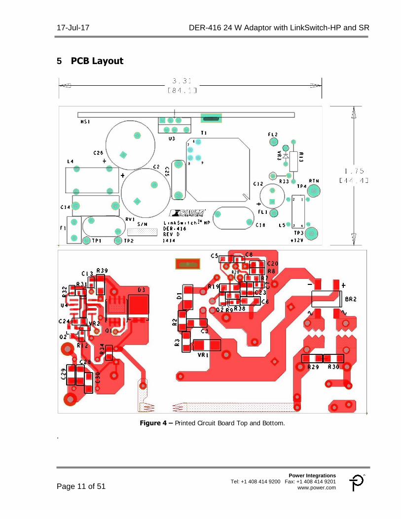
5 PCB Layout
Figure 4 – Printed Circuit Board Top and Bottom.
.
DER-416 24 W Adaptor with LinkSwitch-HP and SR 17-Jul-17
Page 12 of 51
Power Integrations, Inc. Tel: +1 408 414 9200 Fax: +1 408 414 9201 www.power.com
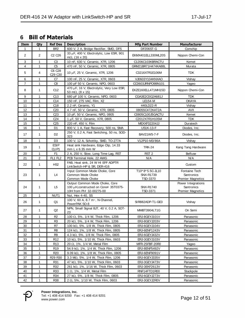
6 Bill of Materials Item Qty Ref Des Description Mfg Part Number Manufacturer
1 1 BR2 600 V, 2 A, Bridge Rectifier, SMD, DFS DF206ST-G Comchip
2 2 C2 C26 33 F, 400 V, Electrolytic, Low ESR, 901 m, (16 x 20) EKMX401ELL330ML20S Nippon Chemi-Con
3 1 C3 10 nF, 630 V, Ceramic, X7R, 1206 C1206C103KBRACTU Kemet 4 1 C5 470 nF, 50 V, Ceramic, X7R, 0805 GRM21BR71H474KA88L Murata
5 4 C6 C28 C29 C30 10 F, 25 V, Ceramic, X7R, 1206 C3216X7R1E106M TDK
6 1 C7 100 nF, 25 V, Ceramic, X7R, 0603 VJ0603Y104KNXAO Vishay 7 1 C8 100 pF 50 V, Ceramic, NPO, 0603 CC0603JRNPO9BN101 Yageo
8 1 C12 470 F, 16 V, Electrolytic, Very Low ESR, 53 m, (8 x 15) EKZE160ELL471MH15D Nippon Chemi-Con
9 1 C13 680 pF 100 V, Ceramic, NPO, 0603 CGA3E2C0G2A681J TDK 10 1 C14 150 nF, 275 VAC, Film, X2 LE154-M OKAYA 11 1 C18 2.2 nF, Ceramic, Y1 440LD22-R Vishay 12 1 C20 4.7 nF, 50 V, Ceramic, X7R, 0805 08055C472KAT2A AVX 13 1 C23 10 pF, 50 V, Ceramic, NPO, 0805 C0805C100J5GACTU Kemet 14 1 C24 1 F, 50 V, Ceramic, X7R, 0805 C2012X7R1H105M TDK 15 1 C25 220 nF, 450 V, Film MEXXF32204JJ Duratech 16 1 D1 800 V, 1 A, Fast Recovery, 500 ns, SMA US1K-13-F Diodes, Inc.
17 1 D2 250 V, 0.2 A, Fast Switching, 50 ns, SOD-323 BAV21WS-7-F Diodes, Inc.
18 1 D3 100 V, 12 A, Schottky, SMD, TO-277A V12P10-M3/86A Vishay
19 1 ESIP CLIP1
Heat sink Hardware, Edge Clip, 14.33 mm L x 6.35 mm W TRK-24 Kang Tang Hardware
20 1 F1 2 A, 250 V, Slow, Long Time Lag, RST RST 2 Belfuse 21 2 FL1 FL2 PCB Terminal Hole, 22 AWG N/A N/A
22 1 HS2 FAB, Heat sink, 24 W HI EFF ADPTR LinkSwitch-HP & SR, DER-416 Custom
23 1 L4 Input Common Mode Choke, Core Common Mode Choke Common Mode Choke
T10*8*5.5C-JL10 SNX-R1739 TSD-3370
Fontaine Tech Santronics
Premier Magnetics
24 1 L5 Output Common Mode Choke, Core 100 H,constructed on Core# 35T0375-10H from PI# 32-00275-00
SNX-R1740 TSD-3371
Power Integrations Santronics
Premier Magnetics 25 1 NUT1 Nut, Hex 4-40, SS
26 1 Q1 100 V, 60 A, 8.7 m・, N-Channel, PowerPAK SO-8 SIR882ADP-T1-GE3 Vishay
27 1 Q2 NPN, Small Signal BJT, 40 V, 0.2 A, SOT-23 MMBT3904LT1G On Semi
28 1 R2 100 , 5%, 1/4 W, Thick Film, 1206 ERJ-8GEYJ101V Panasonic 29 1 R3 20 k, 5%, 1/4 W, Thick Film, 1206 ERJ-8GEYJ203V Panasonic 30 1 R7 100 k, 5%, 1/8 W, Thick Film, 0805 ERJ-6GEYJ104V Panasonic 31 1 R8 124 k, 1%, 1/8 W, Thick Film, 0805 ERJ-6ENF1243V Panasonic 32 1 R9 4.3 k, 5%, 1/8 W, Thick Film, 0805 ERJ-6GEYJ432V Panasonic 33 1 R12 10 k, 5%, 1/10 W, Thick Film, 0603 ERJ-3GEYJ103V Panasonic 34 1 R13 20 , 1%, 1/4 W, Metal Film MFR-25FBF-20R0 Yageo 35 1 R19 54.9 k, 1%, 1/4 W, Thick Film, 1206 ERJ-8ENF5492V Panasonic 36 1 R20 9.09 k, 1%, 1/8 W, Thick Film, 0805 ERJ-6ENF9091V Panasonic 37 2 R29 R30 3.3 M, 5%, 1/4 W, Thick Film, 1206 ERJ-8GEYJ335V Panasonic 38 1 R31 47 k, 5%, 1/10 W, Thick Film, 0603 ERJ-3GEYJ473V Panasonic 39 1 R32 261 k, 1%, 1/16 W, Thick Film, 0603 ERJ-3EKF2613V Panasonic 40 1 R33 1 , 1%, 1/4 W, Metal Film RNF14FTD1R00 Stackpole 41 1 R34 27 k, 5%, 1/8 W, Thick Film, 0805 ERJ-6GEYJ273V Panasonic 42 1 R38 2 , 5%, 1/10 W, Thick Film, 0603 ERJ-3GEYJ2R0V Panasonic
17-Jul-17 DER-416 24 W Adaptor with LinkSwitch-HP and SR
Page 13 of 51
Power Integrations Tel: +1 408 414 9200 Fax: +1 408 414 9201
www.power.com
43 1 R39 10 , 5%, 1/4 W, Thick Film, 1206 ERJ-8GEYJ100V Panasonic 44 1 RTV1 RTV 670810.10ZCLR Silico RTV670810.10ZCLR GE 45 1 RV1 275 V, 45 J, 10 mm, RADIAL V275LA10P Littlefuse
46 1 SCREW1 SCREW PHIL Flat head, undercut 4-40 X .250 (1/4) SST Any RoHS Compliant Mfg.
47 1 T1 Bobbin, RM8, Vertical, 12 pins Transformer Transformer
RM8/12/1 SNX-R1738 PNK-67751
Schwartzpunkt Santronics
Premier Magnetics
48 1 TP1 Test Point, BLK, Miniature THRU-HOLE MOUNT 5001 Keystone
49 1 TP2 Test Point, WHT, Miniature THRU-HOLE MOUNT 5002 Keystone
50 1 TP3 Test Point, RED, THRU-HOLE MOUNT 5010 Keystone 51 1 TP4 Test Point, BLK, THRU-HOLE MOUNT 5011 Keystone 52 1 U3 LinkSwitch-HP, eSIP-7F LNK6775E Power Integrations 53 1 U4 IC, SECONDARY-SIDE CTRLR, 8SOIC UCC24610DR Texas Instruments 54 1 VR1 130 V, 3 W, 5%, DO214AC (SMA) BZG03C130TR Vishay 55 1 VR2 5.6 V, 5%, 150 mW, SSMINI-2 DZ2S056M0L Panasonic 56 1 VR3 75 V, 500 mW, 5%, DO-35 BZX79-C75 Taiwan Semi
DER-416 24 W Adaptor with LinkSwitch-HP and SR 17-Jul-17
Page 14 of 51
Power Integrations, Inc. Tel: +1 408 414 9200 Fax: +1 408 414 9201 www.power.com
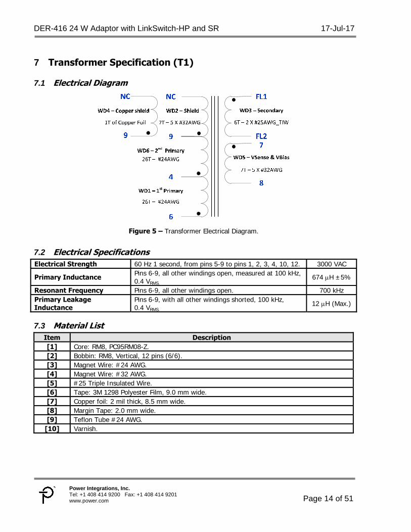
7 Transformer Specification (T1)
7.1 Electrical Diagram
Figure 5 – Transformer Electrical Diagram.
7.2 Electrical Specifications Electrical Strength 60 Hz 1 second, from pins 5-9 to pins 1, 2, 3, 4, 10, 12. 3000 VAC
Primary Inductance Pins 6-9, all other windings open, measured at 100 kHz, 0.4 VRMS.
674 H ±5%
Resonant Frequency Pins 6-9, all other windings open. 700 kHz Primary Leakage Inductance
Pins 6-9, with all other windings shorted, 100 kHz, 0.4 VRMS.
12 H (Max.)
7.3 Material List Item Description [1] Core: RM8, PC95RM08-Z. [2] Bobbin: RM8, Vertical, 12 pins (6/6). [3] Magnet Wire: #24 AWG. [4] Magnet Wire: #32 AWG. [5] #25 Triple Insulated Wire. [6] Tape: 3M 1298 Polyester Film, 9.0 mm wide. [7] Copper foil: 2 mil thick, 8.5 mm wide. [8] Margin Tape: 2.0 mm wide. [9] Teflon Tube #24 AWG.
[10] Varnish.
17-Jul-17 DER-416 24 W Adaptor with LinkSwitch-HP and SR
Page 15 of 51
Power Integrations Tel: +1 408 414 9200 Fax: +1 408 414 9201
www.power.com
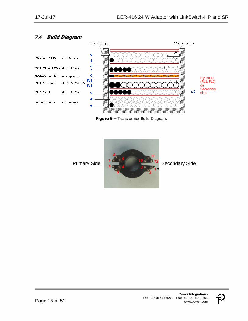
7.4 Build Diagram
Figure 6 – Transformer Build Diagram.
Fly leads (FL1, FL2) on Secondary side
Secondary Side Primary Side
DER-416 24 W Adaptor with LinkSwitch-HP and SR 17-Jul-17
Page 16 of 51
Power Integrations, Inc. Tel: +1 408 414 9200 Fax: +1 408 414 9201 www.power.com
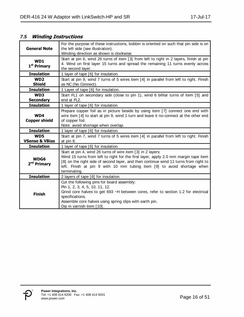
7.5 Winding Instructions
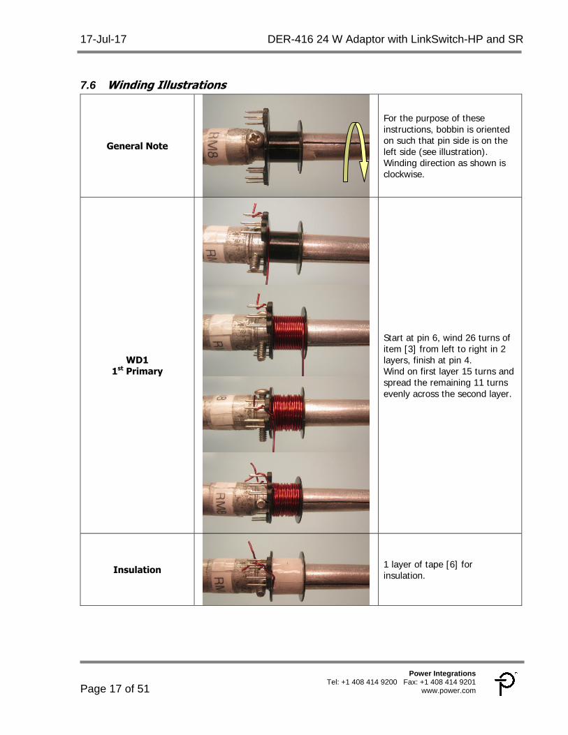
General Note For the purpose of these instructions, bobbin is oriented on such that pin side is on the left side (see illustration). Winding direction as shown is clockwise.
WD1 1st Primary
Start at pin 6, wind 26 turns of item [3] from left to right in 2 layers, finish at pin 4. Wind on first layer 15 turns and spread the remaining 11 turns evenly across the second layer.
Insulation 1 layer of tape [6] for insulation. WD2
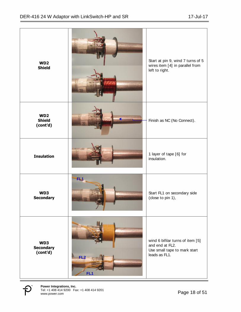
Shield Start at pin 9, wind 7 turns of 5 wires item [4] in parallel from left to right. Finish as NC (No Connect).
Insulation 1 Layer of tape [6] for insulation. WD3
Secondary Start FL1 on secondary side (close to pin 1), wind 6 bifilar turns of item [5] and end at FL2.
Insulation 1 layer of tape [6] for insulation.
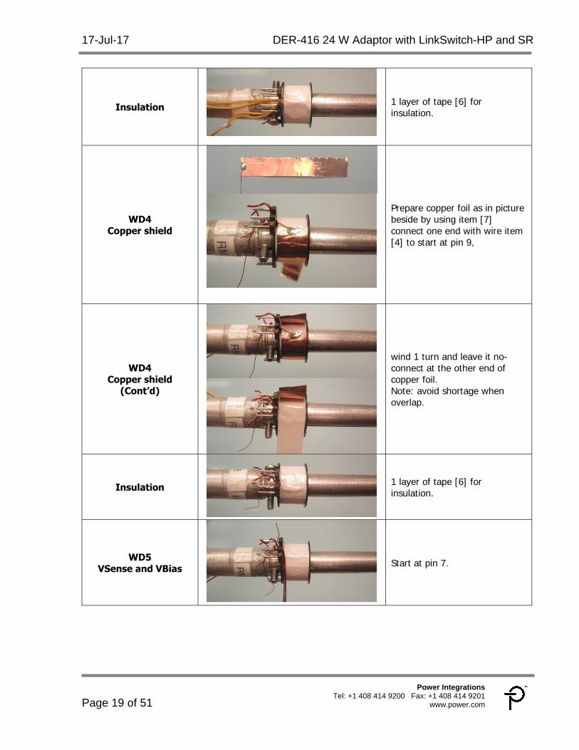
WD4 Copper shield
Prepare copper foil as in picture beside by using item [7] connect one end with wire item [4] to start at pin 9, wind 1 turn and leave it no-connect at the other end of copper foil. Note: avoid shortage when overlap.
Insulation 1 layer of tape [6] for insulation. WD5
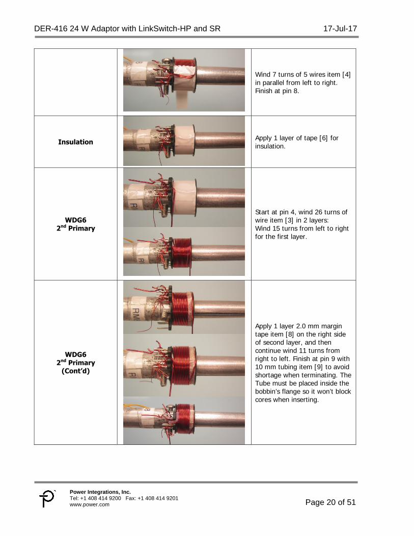
VSense & VBias Start at pin 7, wind 7 turns of 5 wires item [4] in parallel from left to right. Finish at pin 8.
Insulation 1 layer of tape [6] for insulation.
WDG6 2nd Primary
Start at pin 4, wind 26 turns of wire item [3] in 2 layers: Wind 15 turns from left to right for the first layer, apply 2.0 mm margin tape item [8] on the right side of second layer, and then continue wind 11 turns from right to left. Finish at pin 9 with 10 mm tubing item [9] to avoid shortage when terminating.
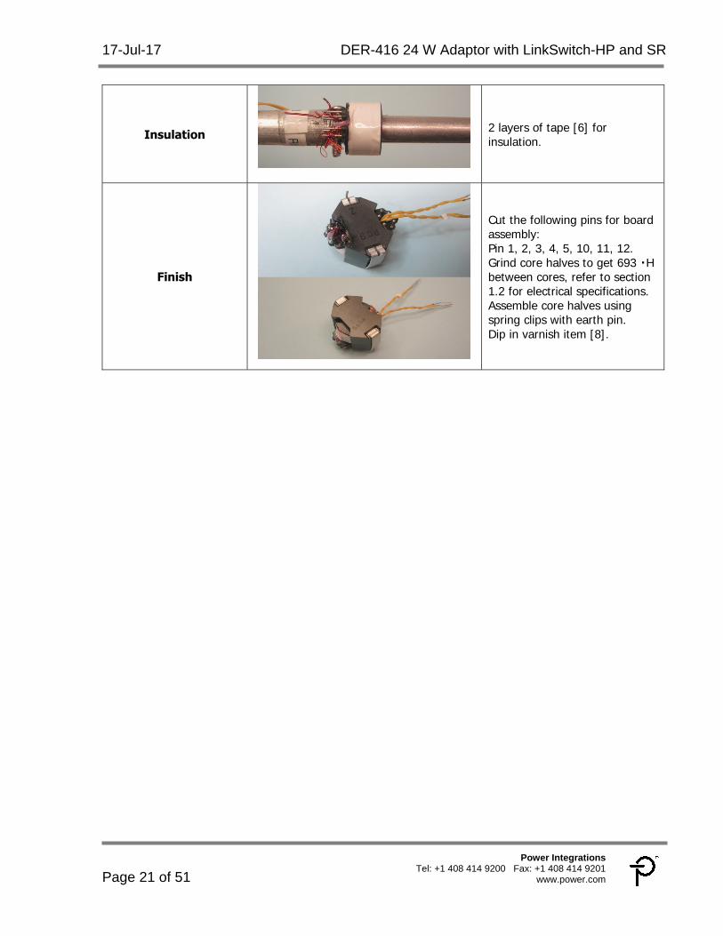
Insulation 2 layers of tape [6] for insulation.
Finish
Cut the following pins for board assembly: Pin 1, 2, 3, 4, 5, 10, 11, 12. Grind core halves to get 693 ・H between cores, refer to section 1.2 for electrical specifications. Assemble core halves using spring clips with earth pin. Dip in varnish item [10].
17-Jul-17 DER-416 24 W Adaptor with LinkSwitch-HP and SR
Page 17 of 51
Power Integrations Tel: +1 408 414 9200 Fax: +1 408 414 9201
www.power.com
7.6 Winding Illustrations
General Note
For the purpose of these instructions, bobbin is oriented on such that pin side is on the left side (see illustration). Winding direction as shown is clockwise.
WD1 1st Primary
Start at pin 6, wind 26 turns of item [3] from left to right in 2 layers, finish at pin 4. Wind on first layer 15 turns and spread the remaining 11 turns evenly across the second layer.
Insulation
1 layer of tape [6] for insulation.
DER-416 24 W Adaptor with LinkSwitch-HP and SR 17-Jul-17
Page 18 of 51
Power Integrations, Inc. Tel: +1 408 414 9200 Fax: +1 408 414 9201 www.power.com
WD2 Shield
Start at pin 9, wind 7 turns of 5 wires item [4] in parallel from left to right.
WD2 Shield
(cont’d)
Finish as NC (No Connect).
Insulation
1 layer of tape [6] for insulation.
WD3 Secondary
Start FL1 on secondary side (close to pin 1),
WD3 Secondary
(cont’d)
wind 6 bifilar turns of item [5] and end at FL2. Use small tape to mark start leads as FL1.
FL1
FL1
FL2
17-Jul-17 DER-416 24 W Adaptor with LinkSwitch-HP and SR
Page 19 of 51
Power Integrations Tel: +1 408 414 9200 Fax: +1 408 414 9201
www.power.com
Insulation
1 layer of tape [6] for insulation.
WD4 Copper shield
Prepare copper foil as in picture beside by using item [7] connect one end with wire item [4] to start at pin 9,
WD4 Copper shield
(Cont’d)
wind 1 turn and leave it no-connect at the other end of copper foil. Note: avoid shortage when overlap.
Insulation
1 layer of tape [6] for insulation.
WD5 VSense and VBias
Start at pin 7.
DER-416 24 W Adaptor with LinkSwitch-HP and SR 17-Jul-17
Page 20 of 51
Power Integrations, Inc. Tel: +1 408 414 9200 Fax: +1 408 414 9201 www.power.com
Wind 7 turns of 5 wires item [4] in parallel from left to right. Finish at pin 8.
Insulation
Apply 1 layer of tape [6] for insulation.
WDG6 2nd Primary
Start at pin 4, wind 26 turns of wire item [3] in 2 layers: Wind 15 turns from left to right for the first layer.
WDG6 2nd Primary
(Cont’d)
Apply 1 layer 2.0 mm margin tape item [8] on the right side of second layer, and then continue wind 11 turns from right to left. Finish at pin 9 with 10 mm tubing item [9] to avoid shortage when terminating. The Tube must be placed inside the bobbin’s flange so it won’t block cores when inserting.
17-Jul-17 DER-416 24 W Adaptor with LinkSwitch-HP and SR
Page 21 of 51
Power Integrations Tel: +1 408 414 9200 Fax: +1 408 414 9201
www.power.com
Insulation
2 layers of tape [6] for insulation.
Finish
Cut the following pins for board assembly: Pin 1, 2, 3, 4, 5, 10, 11, 12. Grind core halves to get 693 ・H between cores, refer to section 1.2 for electrical specifications. Assemble core halves using spring clips with earth pin. Dip in varnish item [8].
DER-416 24 W Adaptor with LinkSwitch-HP and SR 17-Jul-17
Page 22 of 51
Power Integrations, Inc. Tel: +1 408 414 9200 Fax: +1 408 414 9201 www.power.com
1 234
separator
Win
ding
dire
ctio
n
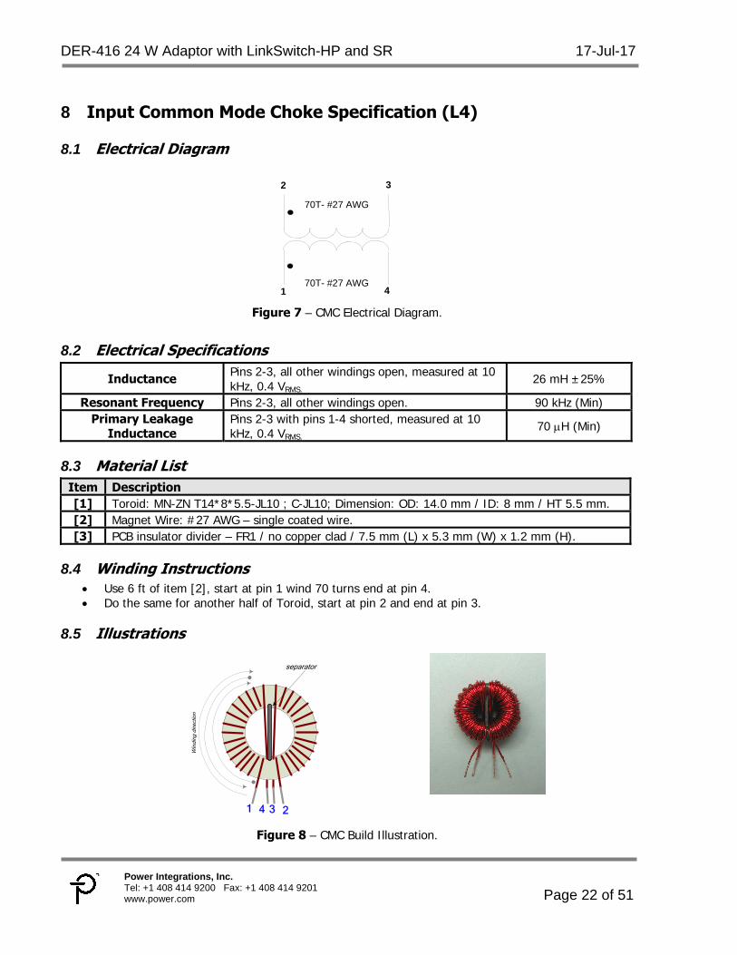
8 Input Common Mode Choke Specification (L4)
8.1 Electrical Diagram
Figure 7 – CMC Electrical Diagram.
8.2 Electrical Specifications
Inductance Pins 2-3, all other windings open, measured at 10 kHz, 0.4 VRMS.
26 mH ±25%
Resonant Frequency Pins 2-3, all other windings open. 90 kHz (Min) Primary Leakage
Inductance Pins 2-3 with pins 1-4 shorted, measured at 10 kHz, 0.4 VRMS.
70 H (Min)
8.3 Material List Item Description [1] Toroid: MN-ZN T14*8*5.5-JL10 ; C-JL10; Dimension: OD: 14.0 mm / ID: 8 mm / HT 5.5 mm. [2] Magnet Wire: #27 AWG – single coated wire. [3] PCB insulator divider – FR1 / no copper clad / 7.5 mm (L) x 5.3 mm (W) x 1.2 mm (H).
8.4 Winding Instructions Use 6 ft of item [2], start at pin 1 wind 70 turns end at pin 4. Do the same for another half of Toroid, start at pin 2 and end at pin 3.
8.5 Illustrations
Figure 8 – CMC Build Illustration.
70T- #27 AWG
2 3
4 1
70T- #27 AWG
17-Jul-17 DER-416 24 W Adaptor with LinkSwitch-HP and SR
Page 23 of 51
Power Integrations Tel: +1 408 414 9200 Fax: +1 408 414 9201
www.power.com
9 Output Common Mode Choke Specification (L5)
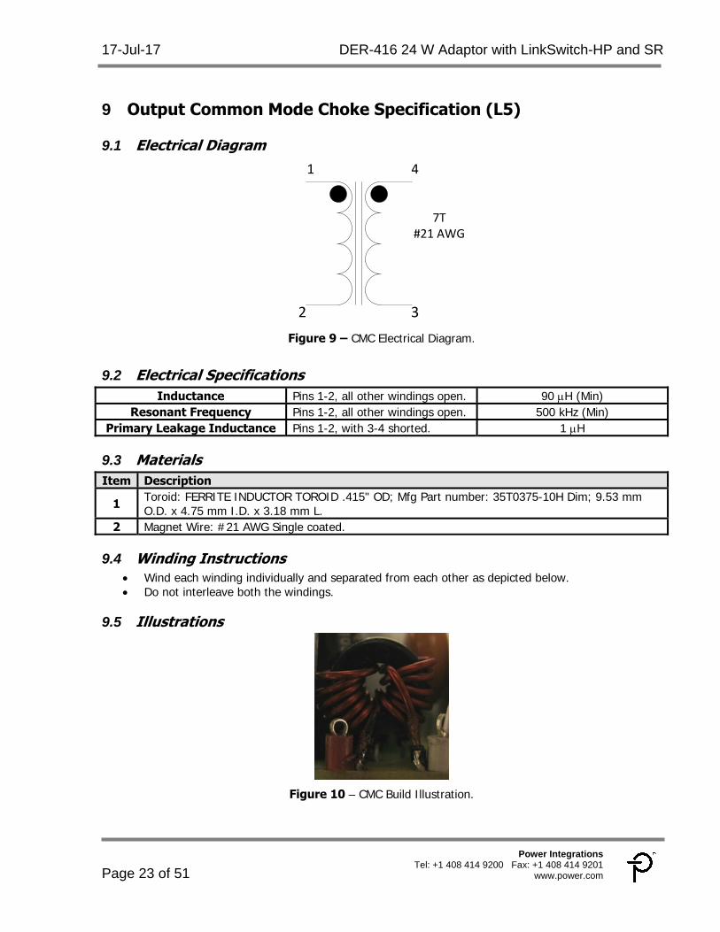
9.1 Electrical Diagram
2
1
3
4
7T#21 AWG
Figure 9 – CMC Electrical Diagram.
9.2 Electrical Specifications Inductance Pins 1-2, all other windings open. 90 H (Min)
Resonant Frequency Pins 1-2, all other windings open. 500 kHz (Min) Primary Leakage Inductance Pins 1-2, with 3-4 shorted. 1 H
9.3 Materials Item Description
1 Toroid: FERRITE INDUCTOR TOROID .415" OD; Mfg Part number: 35T0375-10H Dim; 9.53 mm O.D. x 4.75 mm I.D. x 3.18 mm L.
2 Magnet Wire: #21 AWG Single coated.
9.4 Winding Instructions Wind each winding individually and separated from each other as depicted below. Do not interleave both the windings.
9.5 Illustrations
Figure 10 – CMC Build Illustration.
DER-416 24 W Adaptor with LinkSwitch-HP and SR 17-Jul-17
Page 24 of 51
Power Integrations, Inc. Tel: +1 408 414 9200 Fax: +1 408 414 9201 www.power.com
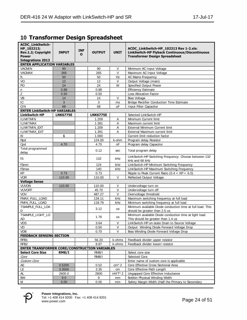
10 Transformer Design Spreadsheet ACDC_LinkSwitch-HP_102213; Rev.1.2; Copyright Power Integrations 2013
INPUT INFO OUTPUT UNIT
ACDC_LinkSwitch-HP_102213 Rev 1-2.xls: LinkSwitch-HP Flyback Continuous/Discontinuous Transformer Design Spreadsheet
ENTER APPLICATION VARIABLES VACMIN 90 90 V Minimum AC Input Voltage VACMAX 265 265 V Maximum AC Input Voltage fL 50 50 Hz AC Mains Frequency VO 12 12 V Output Voltage (main) PO 24 24 W Specified Output Power n 0.88 0.88 Efficiency Estimate Z 0.50 0.50 Loss Allocation Factor VB 14 14 V Bias Voltage tC 3 3 ms Bridge Rectifier Conduction Time Estimate CIN 68 68 uF Input Filter Capacitor ENTER LinkSwitch-HP VARIABLES LinkSwitch-HP LNK6775E LNK6775E Selected LinkSwitch-HP ILIMITMIN 1.209 A Minimum Current limit ILIMITMAX 1.391 A Maximum current limit ILIMITMIN_EXT 1.209 A External Minimum Current limit ILIMITMAX_EXT 1.391 A External Maximum current limit KI 1 1.000 Current limit reduction factor Rpd 124.00 k-ohm Program delay Resistor Cpd 4.70 4.70 nF Program delay Capacitor Total programmed delay 0.12 sec Total program delay
fS 132 kHz LinkSwitch-HP Switching Frequency: Choose between 132 kHz and 66 kHz
fSmin 124 kHz LinkSwitch-HP Minimum Switching Frequency fSmax 140 kHz LinkSwitch-HP Maximum Switching Frequency KP 0.73 0.73 Ripple to Peak Current Ratio (0.4 < KP < 6.0) VOR 110.00 110.00 V Reflected Output Voltage Voltage Sense VUVON 110.00 110.00 V Undervoltage turn on VUVOFF 45.70 V Undervoltage turn off VOV 487.27 V Overvoltage threshold FMAX_FULL_LOAD 134.11 kHz Maximum switching frequency at full load FMIN_FULL_LOAD 118.79 kHz Minimum switching frequency at full load TSAMPLE_FULL_LOAD 3.12 us Minimum available Diode conduction time at full load. This
should be greater than 2.5 us TSAMPLE_LIGHT_LOAD 1.76 us Minimum available Diode conduction time at light load.
This should be greater than 1.4 us VDS 3.64 V LinkSwitch-HP on-state Drain to Source Voltage VD 0.50 V Output Winding Diode Forward Voltage Drop VDB 0.70 V Bias Winding Diode Forward Voltage Drop FEEDBACK SENSING SECTION RFB1 56.20 k-ohms Feedback divider upper resistor RFB2 8.87 k-ohms Feedback divider lowerr resistor ENTER TRANSFORMER CORE/CONSTRUCTION VARIABLES Select Core Size RM8/I RM8/I Select core size Core RM8/I Selected Core Custom Core Enter name of custom core is applicable AE 0.5200 0.52 cm^2 Core Effective Cross Sectional Area LE 3.3500 3.35 cm Core Effective Path Length AL 2600.0 2600 nH/T^2 Ungapped Core Effective Inductance BW 9.0 9 mm Bobbin Physical Winding Width M 0.00 0.00 mm Safety Margin Width (Half the Primary to Secondary
17-Jul-17 DER-416 24 W Adaptor with LinkSwitch-HP and SR
Page 25 of 51
Power Integrations Tel: +1 408 414 9200 Fax: +1 408 414 9201
www.power.com
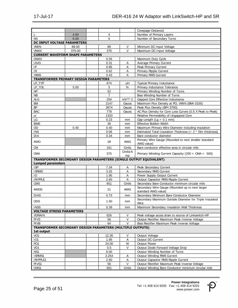
Creepage Distance) L 4.00 4 Number of Primary Layers NS 6.00 6 Number of Secondary Turns DC INPUT VOLTAGE PARAMETERS VMIN 89.00 89 V Minimum DC Input Voltage VMAX 375.00 375 V Maximum DC Input Voltage CURRENT WAVEFORM SHAPE PARAMETERS DMAX 0.56 Maximum Duty Cycle IAVG 0.31 A Average Primary Current IP 0.85 A Peak Primary Current IR 0.62 A Primary Ripple Current IRMS 0.43 A Primary RMS Current TRANSFORMER PRIMARY DESIGN PARAMETERS LP_TYP 674 uH Typical Primary Inductance LP_TOL 5.00 5 % Primary inductance Tolerance NP 52 Primary Winding Number of Turns NB 7 Bias Winding Number of Turns ALG 254 nH/T^2 Gapped Core Effective Inductance BM 2147 Gauss Maximum Flux Density at PO, VMIN (BM<3100) BP 3674 Gauss Peak Flux Density (BP<3700) BAC 778 Gauss AC Flux Density for Core Loss Curves (0.5 X Peak to Peak) ur 1333 Relative Permeability of Ungapped Core LG 0.23 mm Gap Length (Lg > 0.1 mm) BWE 36 mm Effective Bobbin Width OD 0.40 0.40 mm Maximum Primary Wire Diameter including insulation INS 0.06 mm Estimated Total Insulation Thickness (= 2 * film thickness) DIA 0.34 mm Bare conductor diameter
AWG 28 AWG Primary Wire Gauge (Rounded to next smaller standard AWG value)
CM 161 Cmils Bare conductor effective area in circular mils
CMA 375 Cmils/Amp Primary Winding Current Capacity (200 < CMA < 500)
TRANSFORMER SECONDARY DESIGN PARAMETERS (SINGLE OUTPUT EQUIVALENT) Lumped parameters ISP 7.34 A Peak Secondary Current ISRMS 3.25 A Secondary RMS Current IO 1.95 A Power Supply Output Current IRIPPLE 2.60 A Output Capacitor RMS Ripple Current CMS 651 Cmils Secondary Bare Conductor minimum circular mils
AWGS 21 AWG Secondary Wire Gauge (Rounded up to next larger standard AWG value)
DIAS 0.73 mm Secondary Minimum Bare Conductor Diameter
ODS 1.50 mm Secondary Maximum Outside Diameter for Triple Insulated Wire
INSS 0.39 mm Maximum Secondary Insulation Wall Thickness VOLTAGE STRESS PARAMETERS VDRAIN 626 V Peak voltage acoss drain to source of Linkswitch-HP PIVS 56 V Output Rectifier Maximum Peak Inverse Voltage PIVB 64 V Bias Rectifier Maximum Peak Inverse Voltage TRANSFORMER SECONDARY DESIGN PARAMETERS (MULTIPLE OUTPUTS) 1st output VO1 12.30 V Output Voltage IO1 1.95 A Output DC Current PO1 24.00 W Output Power VD1 0.5 V Output Diode Forward Voltage Drop NS1 6.00 Output Winding Number of Turns ISRMS1 3.254 A Output Winding RMS Current IRIPPLE1 2.60 A Output Capacitor RMS Ripple Current PIVS1 56 V Output Rectifier Maximum Peak Inverse Voltage CMS1 651 Cmils Output Winding Bare Conductor minimum circular mils

DER-416 24 W Adaptor with LinkSwitch-HP and SR 17-Jul-17
Page 26 of 51
Power Integrations, Inc. Tel: +1 408 414 9200 Fax: +1 408 414 9201 www.power.com
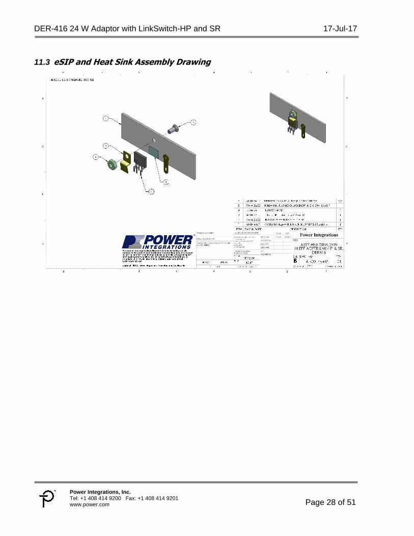
11 eSIP Heat Sink Assemblies
11.1 Heat Sink Fabrication Drawing
17-Jul-17 DER-416 24 W Adaptor with LinkSwitch-HP and SR
Page 27 of 51
Power Integrations Tel: +1 408 414 9200 Fax: +1 408 414 9201
www.power.com
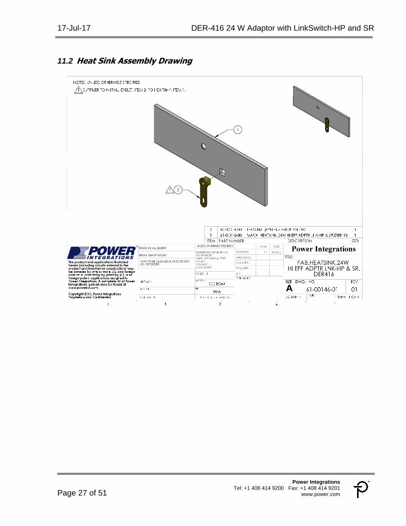
11.2 Heat Sink Assembly Drawing
DER-416 24 W Adaptor with LinkSwitch-HP and SR 17-Jul-17
Page 28 of 51
Power Integrations, Inc. Tel: +1 408 414 9200 Fax: +1 408 414 9201 www.power.com
11.3 eSIP and Heat Sink Assembly Drawing
17-Jul-17 DER-416 24 W Adaptor with LinkSwitch-HP and SR
Page 29 of 51
Power Integrations Tel: +1 408 414 9200 Fax: +1 408 414 9201
www.power.com
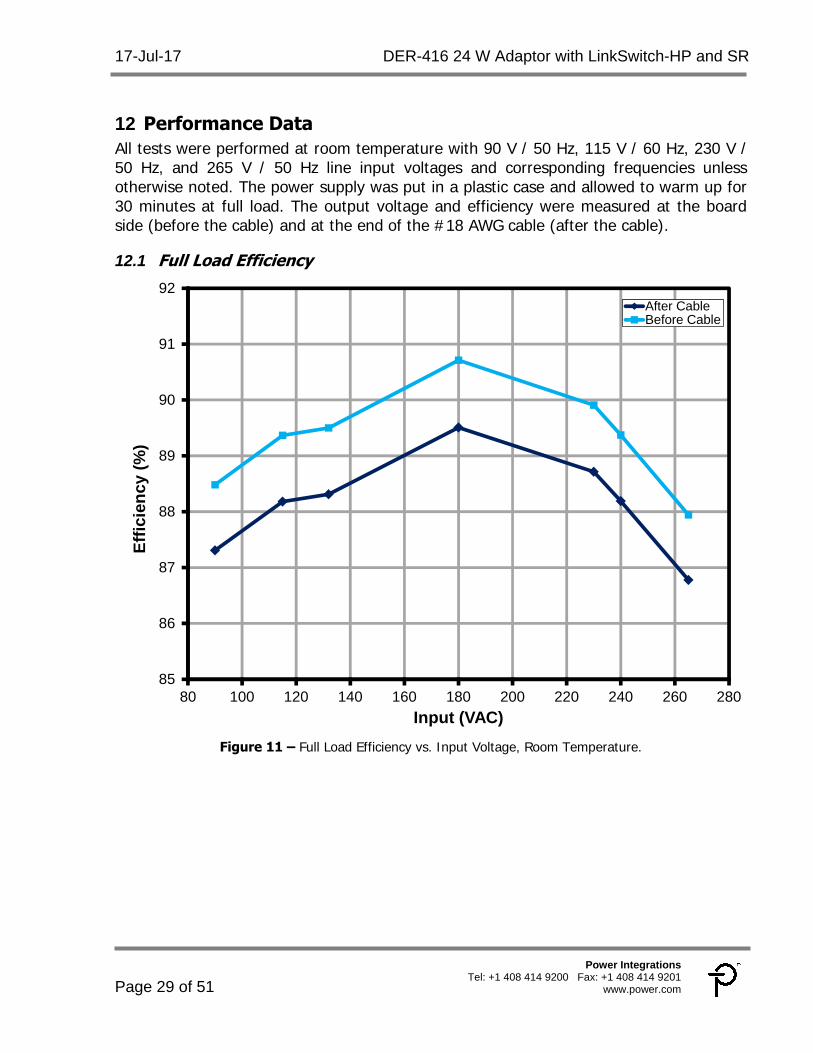
12 Performance Data All tests were performed at room temperature with 90 V / 50 Hz, 115 V / 60 Hz, 230 V / 50 Hz, and 265 V / 50 Hz line input voltages and corresponding frequencies unless otherwise noted. The power supply was put in a plastic case and allowed to warm up for 30 minutes at full load. The output voltage and efficiency were measured at the board side (before the cable) and at the end of the #18 AWG cable (after the cable).
12.1 Full Load Efficiency
85
86
87
88
89
90
91
92
80 100 120 140 160 180 200 220 240 260 280
Eff
icie
ncy
(%
)
Input (VAC)
After CableBefore Cable
Figure 11 – Full Load Efficiency vs. Input Voltage, Room Temperature.
DER-416 24 W Adaptor with LinkSwitch-HP and SR 17-Jul-17
Page 30 of 51
Power Integrations, Inc. Tel: +1 408 414 9200 Fax: +1 408 414 9201 www.power.com
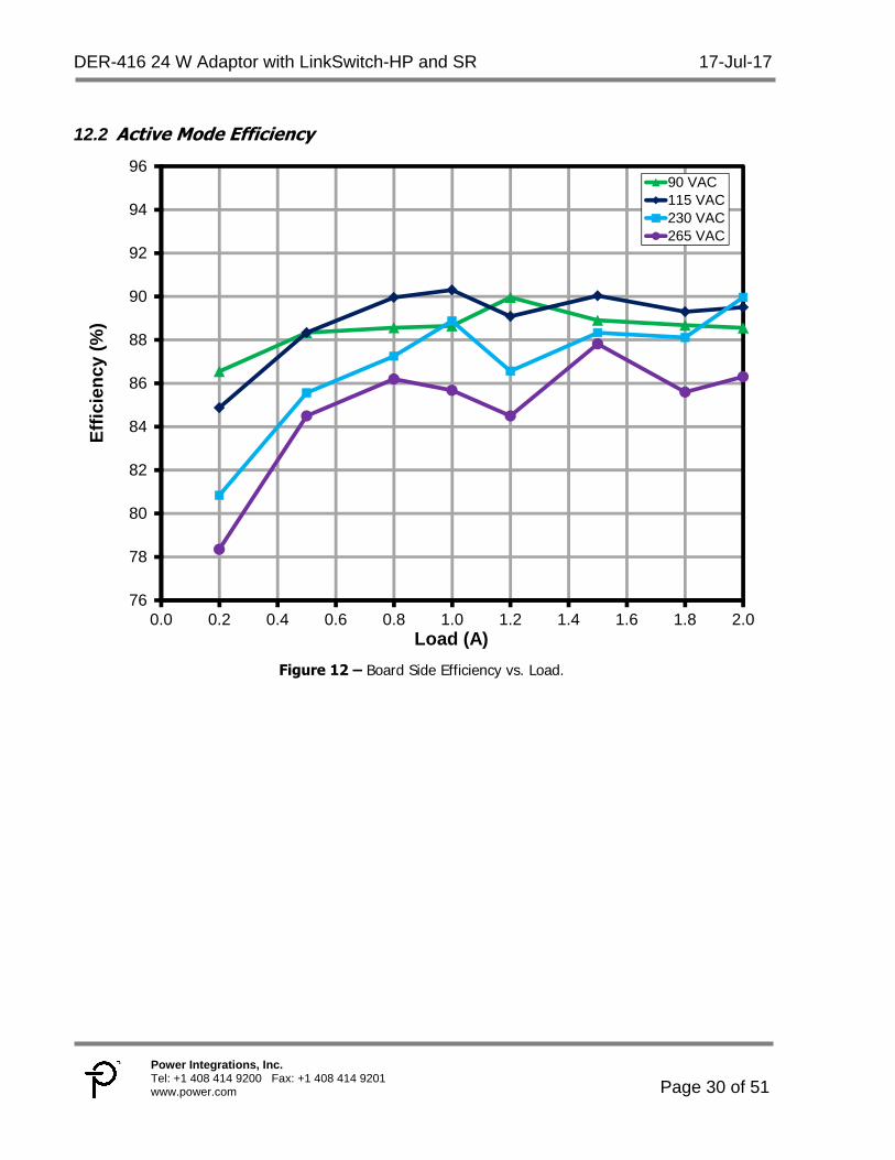
12.2 Active Mode Efficiency
76
78
80
82
84
86
88
90
92
94
96
0.0 0.2 0.4 0.6 0.8 1.0 1.2 1.4 1.6 1.8 2.0
Eff
icie
ncy
(%
)
Load (A)
90 VAC115 VAC230 VAC265 VAC
Figure 12 – Board Side Efficiency vs. Load.
17-Jul-17 DER-416 24 W Adaptor with LinkSwitch-HP and SR
Page 31 of 51
Power Integrations Tel: +1 408 414 9200 Fax: +1 408 414 9201
www.power.com
76
78
80
82
84
86
88
90
92
94
96
0.0 0.2 0.4 0.6 0.8 1.0 1.2 1.4 1.6 1.8 2.0
Eff
icie
ncy
(%
)
Load (A)
90 VAC115 VAC230 VAC265 VAC
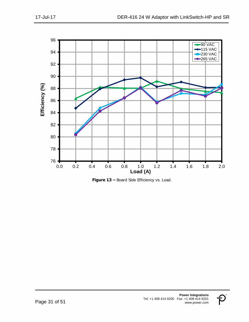
Figure 13 – Board Side Efficiency vs. Load.
DER-416 24 W Adaptor with LinkSwitch-HP and SR 17-Jul-17
Page 32 of 51
Power Integrations, Inc. Tel: +1 408 414 9200 Fax: +1 408 414 9201 www.power.com
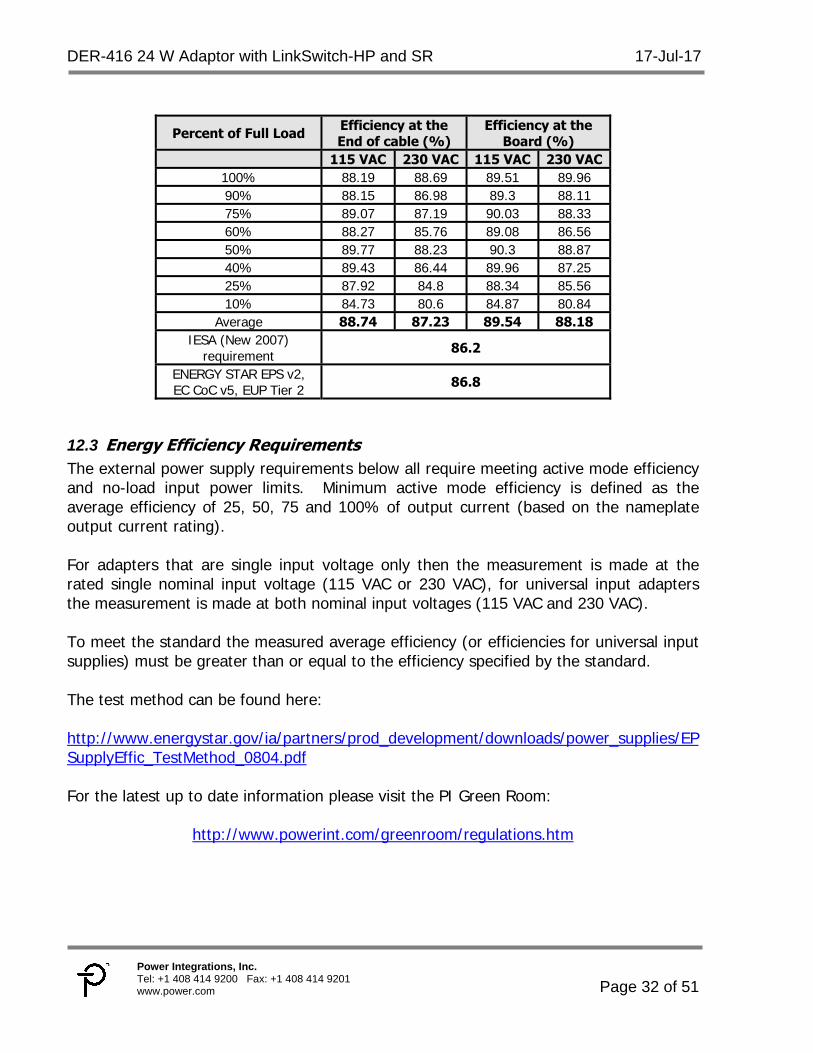
Percent of Full Load Efficiency at the End of cable (%)
Efficiency at the Board (%)
115 VAC 230 VAC 115 VAC 230 VAC 100% 88.19 88.69 89.51 89.96 90% 88.15 86.98 89.3 88.11 75% 89.07 87.19 90.03 88.33 60% 88.27 85.76 89.08 86.56 50% 89.77 88.23 90.3 88.87 40% 89.43 86.44 89.96 87.25 25% 87.92 84.8 88.34 85.56 10% 84.73 80.6 84.87 80.84
Average 88.74 87.23 89.54 88.18 IESA (New 2007)
requirement 86.2
ENERGY STAR EPS v2, EC CoC v5, EUP Tier 2 86.8
12.3 Energy Efficiency Requirements The external power supply requirements below all require meeting active mode efficiency and no-load input power limits. Minimum active mode efficiency is defined as the average efficiency of 25, 50, 75 and 100% of output current (based on the nameplate output current rating). For adapters that are single input voltage only then the measurement is made at the rated single nominal input voltage (115 VAC or 230 VAC), for universal input adapters the measurement is made at both nominal input voltages (115 VAC and 230 VAC). To meet the standard the measured average efficiency (or efficiencies for universal input supplies) must be greater than or equal to the efficiency specified by the standard. The test method can be found here: http://www.energystar.gov/ia/partners/prod_development/downloads/power_supplies/EPSupplyEffic_TestMethod_0804.pdf For the latest up to date information please visit the PI Green Room:
http://www.powerint.com/greenroom/regulations.htm
17-Jul-17 DER-416 24 W Adaptor with LinkSwitch-HP and SR
Page 33 of 51
Power Integrations Tel: +1 408 414 9200 Fax: +1 408 414 9201
www.power.com
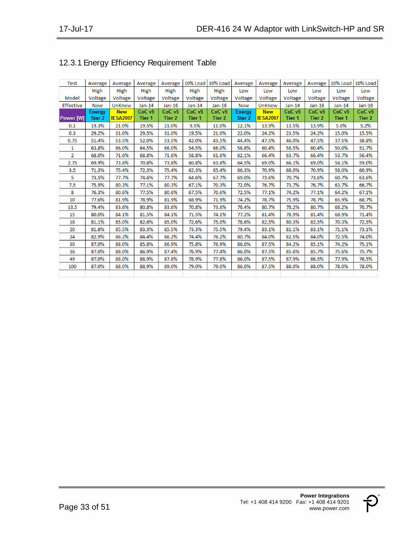
12.3.1 Energy Efficiency Requirement Table
DER-416 24 W Adaptor with LinkSwitch-HP and SR 17-Jul-17
Page 34 of 51
Power Integrations, Inc. Tel: +1 408 414 9200 Fax: +1 408 414 9201 www.power.com
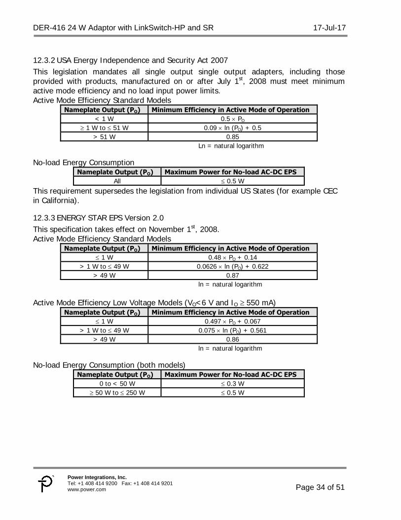
12.3.2 USA Energy Independence and Security Act 2007 This legislation mandates all single output single output adapters, including those provided with products, manufactured on or after July 1st, 2008 must meet minimum active mode efficiency and no load input power limits. Active Mode Efficiency Standard Models
Nameplate Output (PO) Minimum Efficiency in Active Mode of Operation < 1 W 0.5 PO
1 W to 51 W 0.09 ln (PO) + 0.5 > 51 W 0.85
Ln = natural logarithm No-load Energy Consumption
Nameplate Output (PO) Maximum Power for No-load AC-DC EPS All 0.5 W
This requirement supersedes the legislation from individual US States (for example CEC in California).
12.3.3 ENERGY STAR EPS Version 2.0 This specification takes effect on November 1st, 2008. Active Mode Efficiency Standard Models
Nameplate Output (PO) Minimum Efficiency in Active Mode of Operation 1 W 0.48 PO + 0.14
> 1 W to 49 W 0.0626 ln (PO) + 0.622 > 49 W 0.87
ln = natural logarithm Active Mode Efficiency Low Voltage Models (VO<6 V and IO 550 mA)
Nameplate Output (PO) Minimum Efficiency in Active Mode of Operation 1 W 0.497 PO + 0.067
> 1 W to 49 W 0.075 ln (PO) + 0.561 > 49 W 0.86
ln = natural logarithm No-load Energy Consumption (both models)
Nameplate Output (PO) Maximum Power for No-load AC-DC EPS 0 to < 50 W 0.3 W
50 W to 250 W 0.5 W
17-Jul-17 DER-416 24 W Adaptor with LinkSwitch-HP and SR
Page 35 of 51
Power Integrations Tel: +1 408 414 9200 Fax: +1 408 414 9201
www.power.com
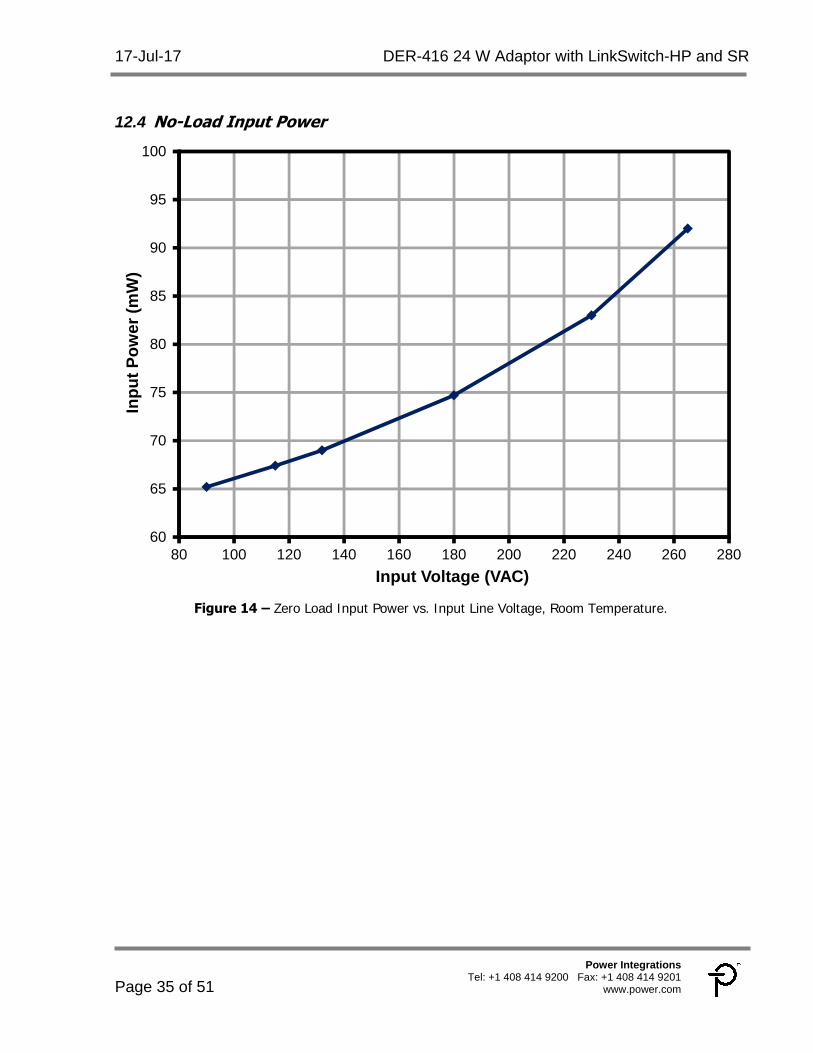
12.4 No-Load Input Power
60
65
70
75
80
85
90
95
100
80 100 120 140 160 180 200 220 240 260 280
Inp
ut
Po
wer
(m
W)
Input Voltage (VAC) Figure 14 – Zero Load Input Power vs. Input Line Voltage, Room Temperature.
DER-416 24 W Adaptor with LinkSwitch-HP and SR 17-Jul-17
Page 36 of 51
Power Integrations, Inc. Tel: +1 408 414 9200 Fax: +1 408 414 9201 www.power.com
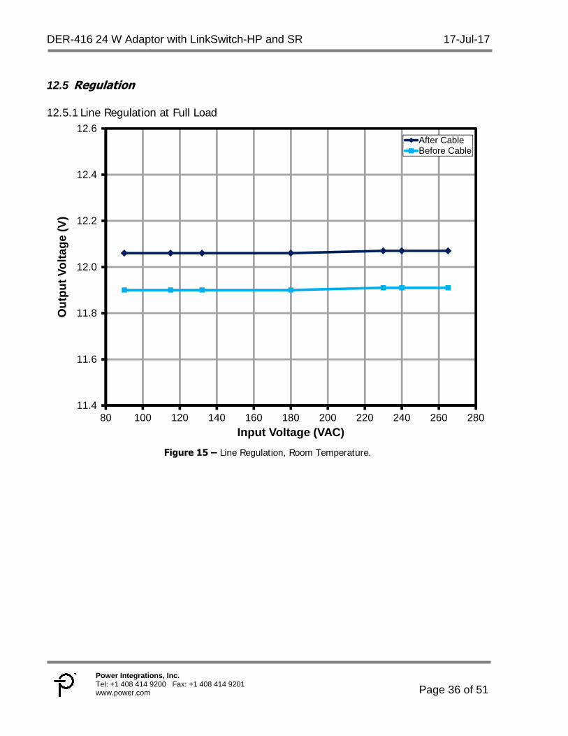
12.5 Regulation
12.5.1 Line Regulation at Full Load
11.4
11.6
11.8
12.0
12.2
12.4
12.6
80 100 120 140 160 180 200 220 240 260 280
Ou
tpu
t V
olt
age
(V)
Input Voltage (VAC)
After CableBefore Cable
Figure 15 – Line Regulation, Room Temperature.
17-Jul-17 DER-416 24 W Adaptor with LinkSwitch-HP and SR
Page 37 of 51
Power Integrations Tel: +1 408 414 9200 Fax: +1 408 414 9201
www.power.com
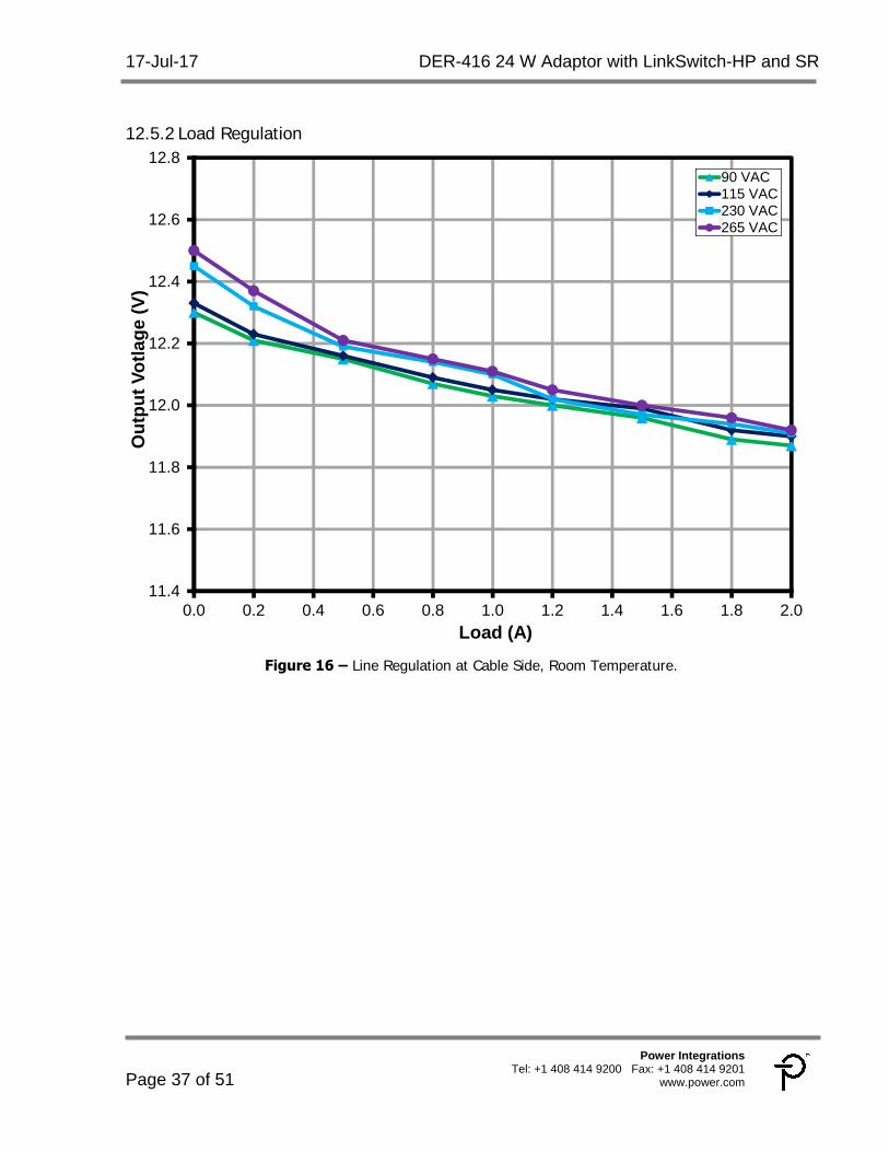
12.5.2 Load Regulation
11.4
11.6
11.8
12.0
12.2
12.4
12.6
12.8
0.0 0.2 0.4 0.6 0.8 1.0 1.2 1.4 1.6 1.8 2.0
Ou
tpu
t V
otl
age
(V)
Load (A)
90 VAC115 VAC230 VAC265 VAC
Figure 16 – Line Regulation at Cable Side, Room Temperature.
DER-416 24 W Adaptor with LinkSwitch-HP and SR 17-Jul-17
Page 38 of 51
Power Integrations, Inc. Tel: +1 408 414 9200 Fax: +1 408 414 9201 www.power.com
11.4
11.6
11.8
12.0
12.2
12.4
12.6
12.8
0.0 0.2 0.4 0.6 0.8 1.0 1.2 1.4 1.6 1.8 2.0
Ou
tpu
t V
otl
age
(V)
Load (A)
90 VAC115 VAC230 VAC265 VAC
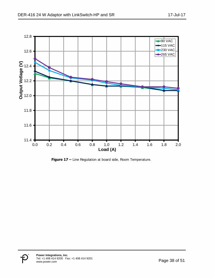
Figure 17 – Line Regulation at board side, Room Temperature.
17-Jul-17 DER-416 24 W Adaptor with LinkSwitch-HP and SR
Page 39 of 51
Power Integrations Tel: +1 408 414 9200 Fax: +1 408 414 9201
www.power.com
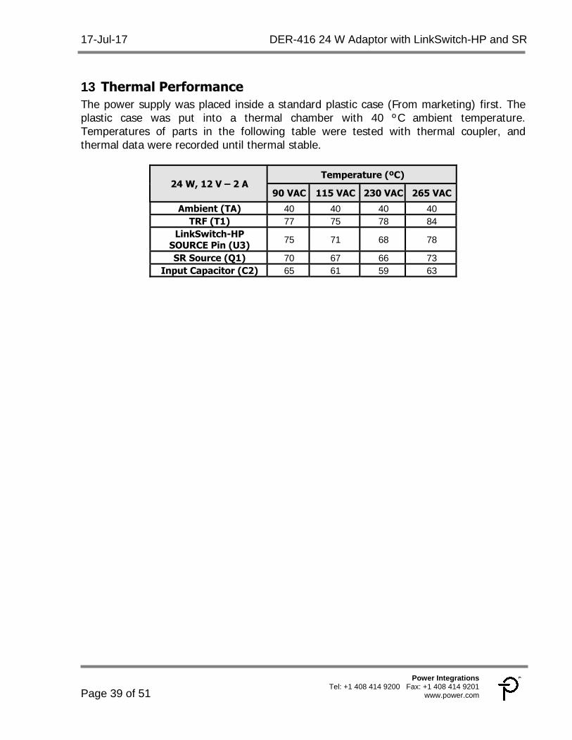
13 Thermal Performance The power supply was placed inside a standard plastic case (From marketing) first. The plastic case was put into a thermal chamber with 40 ºC ambient temperature. Temperatures of parts in the following table were tested with thermal coupler, and thermal data were recorded until thermal stable.
24 W, 12 V – 2 A Temperature (ºC)
90 VAC 115 VAC 230 VAC 265 VAC
Ambient (TA) 40 40 40 40 TRF (T1) 77 75 78 84
LinkSwitch-HP SOURCE Pin (U3) 75 71 68 78
SR Source (Q1) 70 67 66 73 Input Capacitor (C2) 65 61 59 63
DER-416 24 W Adaptor with LinkSwitch-HP and SR 17-Jul-17
Page 40 of 51
Power Integrations, Inc. Tel: +1 408 414 9200 Fax: +1 408 414 9201 www.power.com
14 Waveforms
14.1 Drain Voltage and Current, Normal Operation
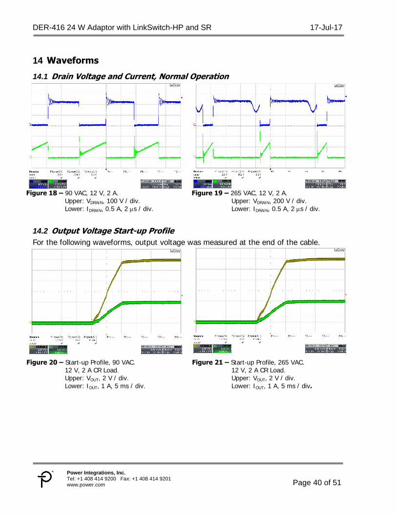
Figure 18 – 90 VAC, 12 V, 2 A.
Upper: VDRAIN, 100 V / div. Lower: IDRAIN, 0.5 A, 2 s / div.
Figure 19 – 265 VAC, 12 V, 2 A. Upper: VDRAIN, 200 V / div. Lower: IDRAIN, 0.5 A, 2 s / div.
14.2 Output Voltage Start-up Profile For the following waveforms, output voltage was measured at the end of the cable.
Figure 20 – Start-up Profile, 90 VAC.
12 V, 2 A CR Load. Upper: VOUT, 2 V / div. Lower: IOUT, 1 A, 5 ms / div.
Figure 21 – Start-up Profile, 265 VAC. 12 V, 2 A CR Load. Upper: VOUT, 2 V / div. Lower: IOUT, 1 A, 5 ms / div.
17-Jul-17 DER-416 24 W Adaptor with LinkSwitch-HP and SR
Page 41 of 51
Power Integrations Tel: +1 408 414 9200 Fax: +1 408 414 9201
www.power.com
Figure 22 – Start-up Profile, 90 VAC.
12 V, 0.2 A CR Load. Upper: VOUT, 2 V / div. Lower: IOUT, 0.2 A, 5 ms / div.
Figure 23 – Start-up Profile, 265 VAC. 12 V, 0.2 A CR Load. Upper: VOUT, 2 V / div. Lower: IOUT, 0.2 A, 5 ms / div.
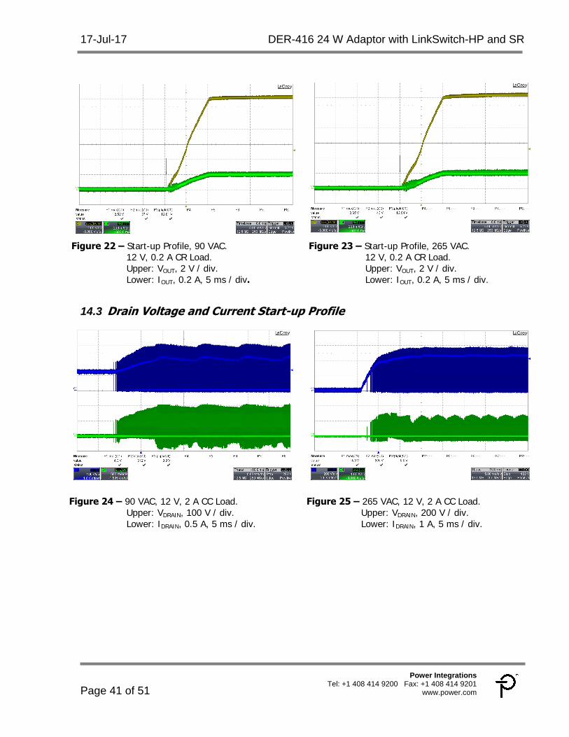
14.3 Drain Voltage and Current Start-up Profile
Figure 24 – 90 VAC, 12 V, 2 A CC Load. Upper: VDRAIN, 100 V / div. Lower: IDRAIN, 0.5 A, 5 ms / div.
Figure 25 – 265 VAC, 12 V, 2 A CC Load. Upper: VDRAIN, 200 V / div. Lower: IDRAIN, 1 A, 5 ms / div.
DER-416 24 W Adaptor with LinkSwitch-HP and SR 17-Jul-17
Page 42 of 51
Power Integrations, Inc. Tel: +1 408 414 9200 Fax: +1 408 414 9201 www.power.com
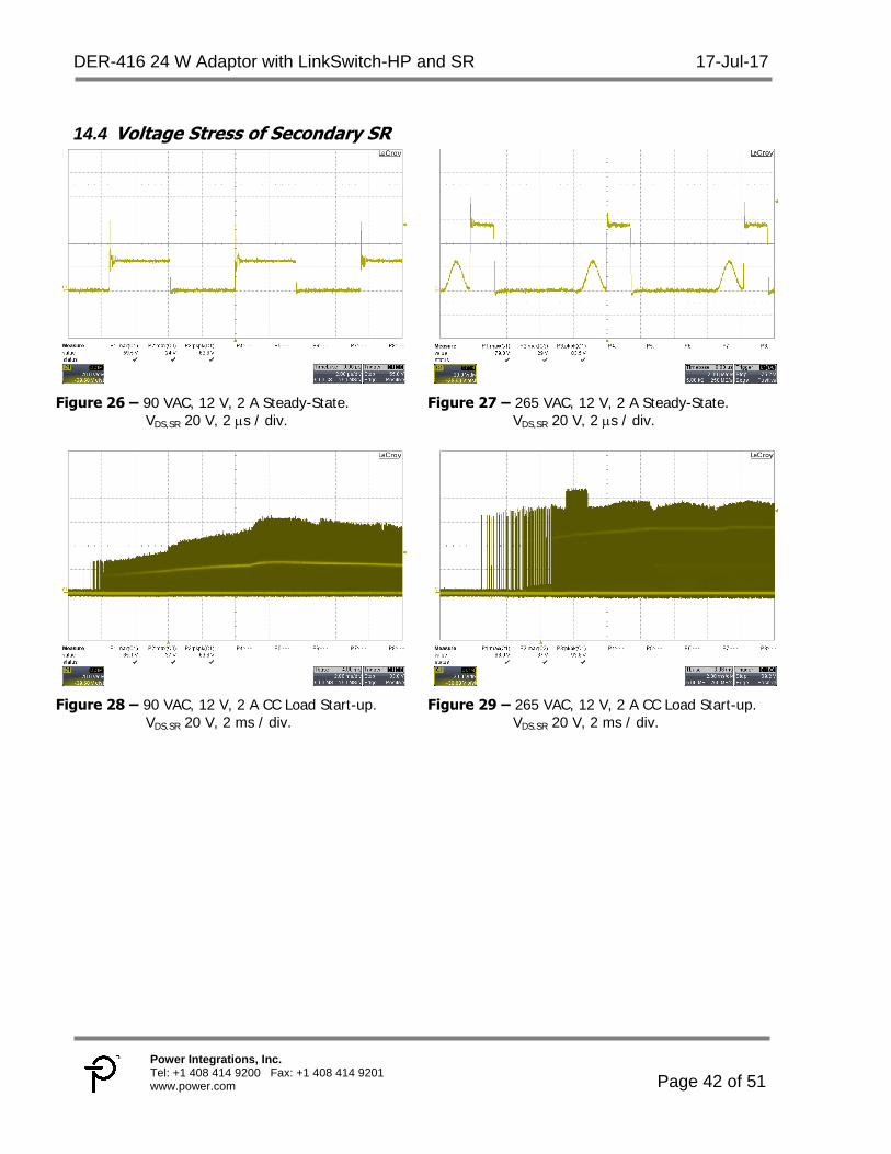
14.4 Voltage Stress of Secondary SR
Figure 26 – 90 VAC, 12 V, 2 A Steady-State.
VDS,SR 20 V, 2 s / div. Figure 27 – 265 VAC, 12 V, 2 A Steady-State.
VDS,SR 20 V, 2 s / div.
Figure 28 – 90 VAC, 12 V, 2 A CC Load Start-up.
VDS,SR 20 V, 2 ms / div. Figure 29 – 265 VAC, 12 V, 2 A CC Load Start-up.
VDS,SR 20 V, 2 ms / div.
17-Jul-17 DER-416 24 W Adaptor with LinkSwitch-HP and SR
Page 43 of 51
Power Integrations Tel: +1 408 414 9200 Fax: +1 408 414 9201
www.power.com
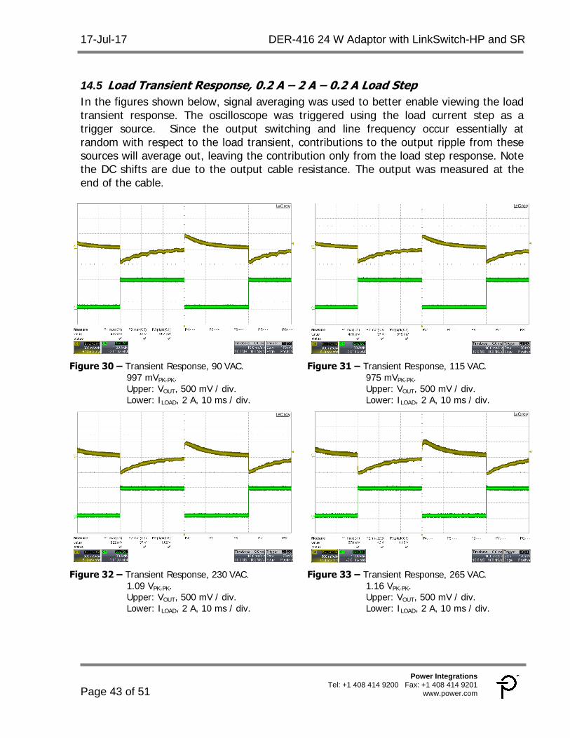
14.5 Load Transient Response, 0.2 A – 2 A – 0.2 A Load Step In the figures shown below, signal averaging was used to better enable viewing the load transient response. The oscilloscope was triggered using the load current step as a trigger source. Since the output switching and line frequency occur essentially at random with respect to the load transient, contributions to the output ripple from these sources will average out, leaving the contribution only from the load step response. Note the DC shifts are due to the output cable resistance. The output was measured at the end of the cable.
Figure 30 – Transient Response, 90VAC.
997 mVPK-PK. Upper: VOUT, 500 mV / div. Lower: ILOAD, 2 A, 10 ms / div.
Figure 31 – Transient Response, 115VAC. 975 mVPK-PK. Upper: VOUT, 500 mV / div. Lower: ILOAD, 2 A, 10 ms / div.
Figure 32 – Transient Response, 230VAC.
1.09 VPK-PK. Upper: VOUT, 500 mV / div. Lower: ILOAD, 2 A, 10 ms / div.
Figure 33 – Transient Response, 265VAC. 1.16 VPK-PK. Upper: VOUT, 500 mV / div. Lower: ILOAD, 2 A, 10 ms / div.
DER-416 24 W Adaptor with LinkSwitch-HP and SR 17-Jul-17
Page 44 of 51
Power Integrations, Inc. Tel: +1 408 414 9200 Fax: +1 408 414 9201 www.power.com
14.6 Output Ripple Measurements
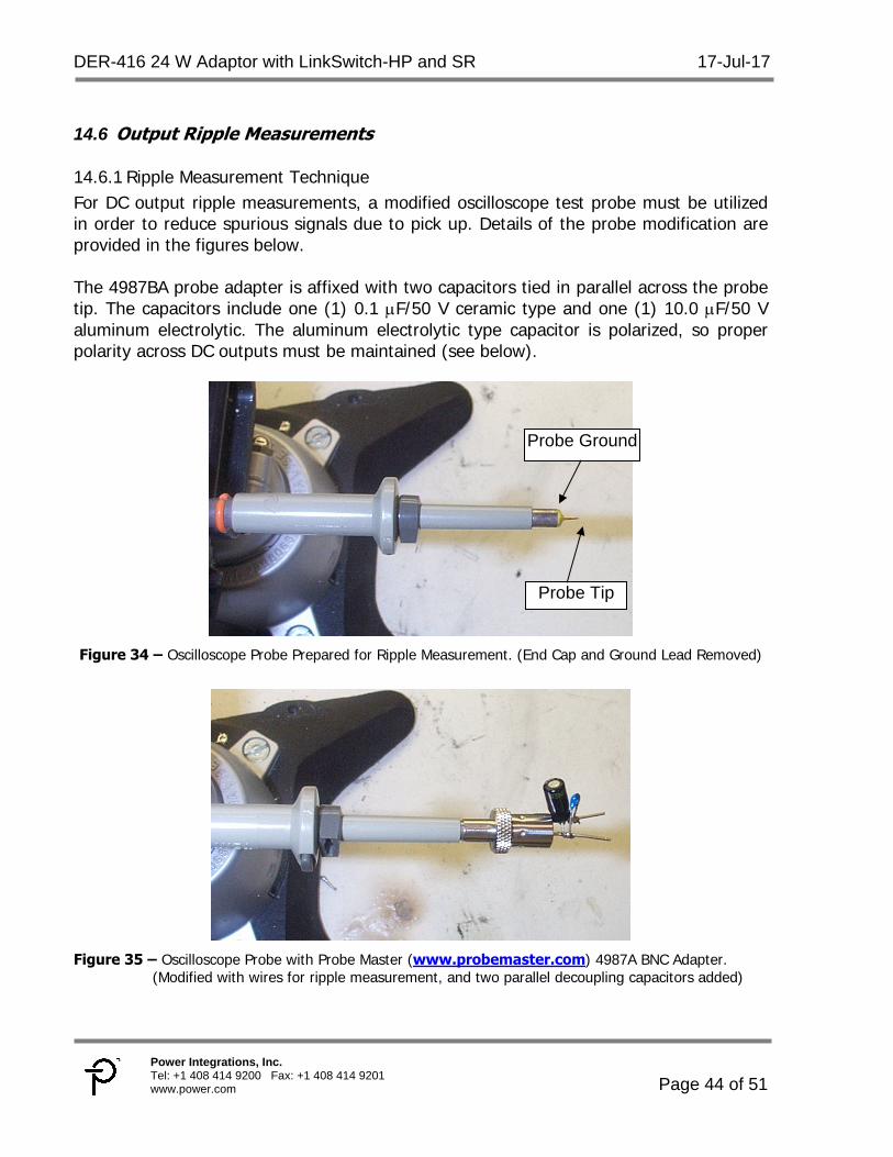
14.6.1 Ripple Measurement Technique For DC output ripple measurements, a modified oscilloscope test probe must be utilized in order to reduce spurious signals due to pick up. Details of the probe modification are provided in the figures below. The 4987BA probe adapter is affixed with two capacitors tied in parallel across the probe tip. The capacitors include one (1) 0.1 F/50 V ceramic type and one (1) 10.0 F/50 V aluminum electrolytic. The aluminum electrolytic type capacitor is polarized, so proper polarity across DC outputs must be maintained (see below).
Figure 34 – Oscilloscope Probe Prepared for Ripple Measurement. (End Cap and Ground Lead Removed)
Figure 35 – Oscilloscope Probe with Probe Master (www.probemaster.com) 4987A BNC Adapter.
(Modified with wires for ripple measurement, and two parallel decoupling capacitors added)
Probe Ground
Probe Tip
17-Jul-17 DER-416 24 W Adaptor with LinkSwitch-HP and SR
Page 45 of 51
Power Integrations Tel: +1 408 414 9200 Fax: +1 408 414 9201
www.power.com
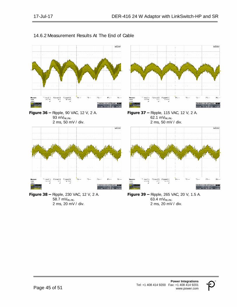
14.6.2 Measurement Results At The End of Cable
Figure 36 – Ripple, 90 VAC, 12 V, 2 A.
93 mVPK-PK. 2 ms, 50 mV / div.
Figure 37 – Ripple, 115 VAC, 12 V, 2 A. 62.1 mVPK-PK. 2 ms, 50 mV / div.
Figure 38 – Ripple, 230 VAC, 12 V, 2 A.
58.7 mVPK-PK. 2 ms, 20 mV / div.
Figure 39 – Ripple, 265 VAC, 20 V, 1.5 A. 63.4 mVPK-PK. 2 ms, 20 mV / div.

DER-416 24 W Adaptor with LinkSwitch-HP and SR 17-Jul-17
Page 46 of 51
Power Integrations, Inc. Tel: +1 408 414 9200 Fax: +1 408 414 9201 www.power.com
15 AC Surge (Resistive Full Load at the Output) During the DM test and Line to PE common mode test, the output is always well regulated. But auto-restart can be found for 6 kV and 6.6 kV surge across Neutral and PE. Tests were run to conform that the auto restart is caused by input OVP which is triggered during the surge across Neutral to PE.
Surge Level (V)
Input Voltage (VAC)
Injection Location
Injection Phase (°)
Test Results (Pass/Fail # Strikes)
D.M. (2Ω source) 10 Strikes Each Level +2000 230 L to N 90 Pass -2000 230 L to N 270 Pass C.M. (12Ω source)
+6000 230 L to PE 90 Pass -6000 230 L to PE 270 Pass +6000 230 N to PE 90 Auto Restart -6000 230 N to PE 270 Auto Restart +6600 230 L to PE 90 Pass -6600 230 L to PE 270 Pass +6600 230 N to PE 90 Auto Restart -6600 230 N to PE 270 Auto Restart
17-Jul-17 DER-416 24 W Adaptor with LinkSwitch-HP and SR
Page 47 of 51
Power Integrations Tel: +1 408 414 9200 Fax: +1 408 414 9201
www.power.com
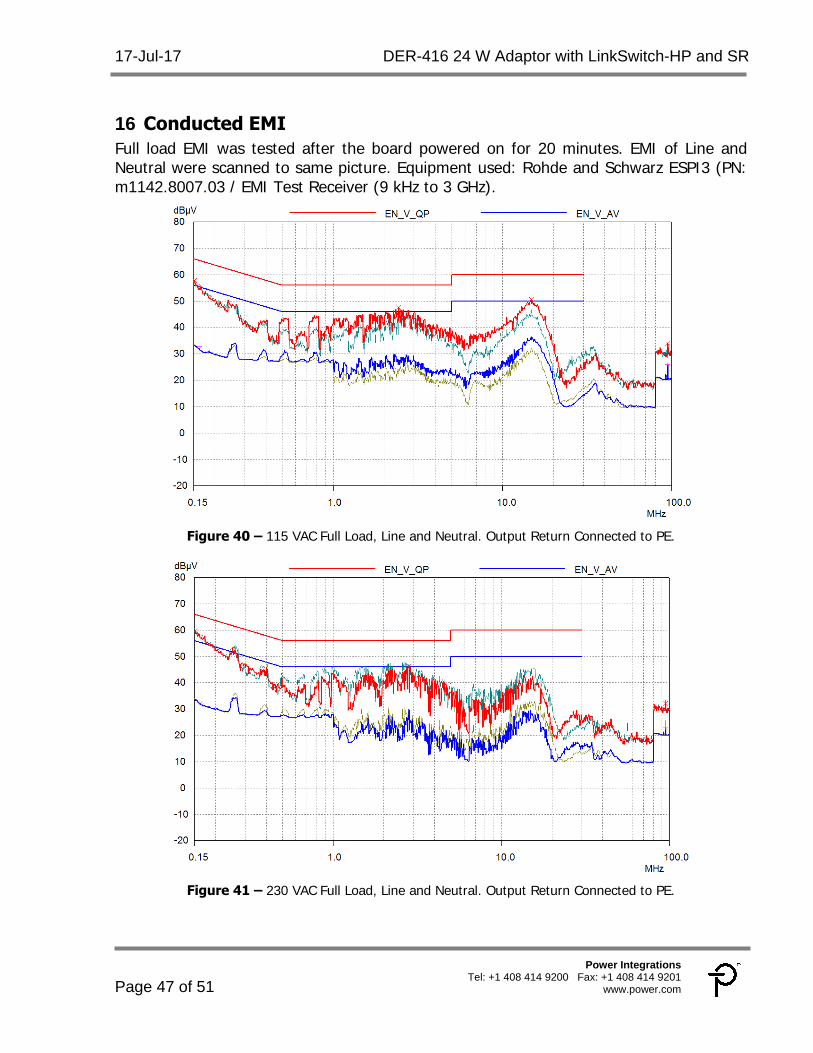
16 Conducted EMI Full load EMI was tested after the board powered on for 20 minutes. EMI of Line and Neutral were scanned to same picture. Equipment used: Rohde and Schwarz ESPI3 (PN: m1142.8007.03 / EMI Test Receiver (9 kHz to 3 GHz).
Figure 40 – 115 VAC Full Load, Line and Neutral. Output Return Connected to PE.
Figure 41 – 230 VAC Full Load, Line and Neutral. Output Return Connected to PE.
DER-416 24 W Adaptor with LinkSwitch-HP and SR 17-Jul-17
Page 48 of 51
Power Integrations, Inc. Tel: +1 408 414 9200 Fax: +1 408 414 9201 www.power.com
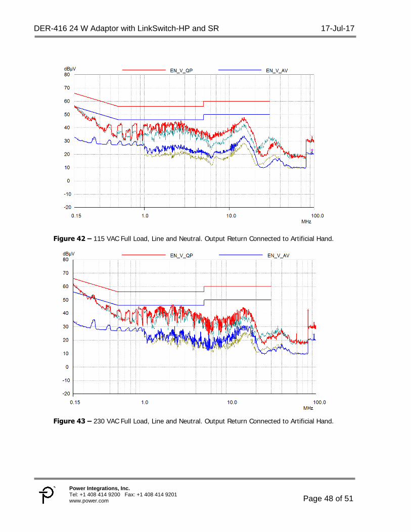
Figure 42 – 115 VAC Full Load, Line and Neutral. Output Return Connected to Artificial Hand.
Figure 43 – 230 VAC Full Load, Line and Neutral. Output Return Connected to Artificial Hand.
17-Jul-17 DER-416 24 W Adaptor with LinkSwitch-HP and SR
Page 49 of 51
Power Integrations Tel: +1 408 414 9200 Fax: +1 408 414 9201
www.power.com
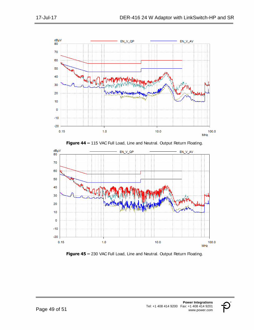
Figure 44 – 115 VAC Full Load, Line and Neutral. Output Return Floating.
Figure 45 – 230 VAC Full Load, Line and Neutral. Output Return Floating.
DER-416 24 W Adaptor with LinkSwitch-HP and SR 17-Jul-17
Page 50 of 51
Power Integrations, Inc. Tel: +1 408 414 9200 Fax: +1 408 414 9201 www.power.com
17 Revision History Date Author Revision Description & changes Reviewed
17-Jul-17 PL 1.5 Initial Release Apps & Mktg
17-Jul-17 DER-416 24 W Adaptor with LinkSwitch-HP and SR
Page 51 of 51
Power Integrations Tel: +1 408 414 9200 Fax: +1 408 414 9201
www.power.com
For the latest updates, visit our website: www.power.com Reference Designs are technical proposals concerning how to use Power Integrations’ gate drivers in particular applications and/or with certain power modules. These proposals are “as is” and are not subject to any qualification process. The suitability, implementation and qualification are the sole responsibility of the end user. The statements, technical information and recommendations contained herein are believed to be accurate as of the date hereof. All parameters, numbers, values and other technical data included in the technical information were calculated and determined to our best knowledge in accordance with the relevant technical norms (if any). They may base on assumptions or operational conditions that do not necessarily apply in general. We exclude any representation or warranty, express or implied, in relation to the accuracy or completeness of the statements, technical information and recommendations contained herein. No responsibility is accepted for the accuracy or sufficiency of any of the statements, technical information, recommendations or opinions communicated and any liability for any direct, indirect or consequential loss or damage suffered by any person arising therefrom is expressly disclaimed. Power Integrations reserves the right to make changes to its products at any time to improve reliability or manufacturability. Power Integrations does not assume any liability arising from the use of any device or circuit described herein. POWER INTEGRATIONS MAKES NO WARRANTY HEREIN AND SPECIFICALLY DISCLAIMS ALL WARRANTIES INCLUDING, WITHOUT LIMITATION, THE IMPLIED WARRANTIES OF MERCHANTABILITY, FITNESS FOR A PARTICULAR PURPOSE, AND NON-INFRINGEMENT OF THIRD PARTY RIGHTS. Patent Information The products and applications illustrated herein (including transformer construction and circuits’ external to the products) may be covered by one or more U.S. and foreign patents, or potentially by pending U.S. and foreign patent applications assigned to Power
Integrations. A complete list of Power Integrations’ patents may be found at www.power.com. Power Integrations grants its
customers a license under certain patent rights as set forth at http://www.power.com/ip.htm.
The PI Logo, TOPSwitch, TinySwitch, LinkSwitch, LYTSwitch, InnoSwtich, DPA-Switch, PeakSwitch, CAPZero, SENZero, LinkZero, HiperPFS, HiperTFS, HiperLCS, Qspeed, EcoSmart, Clampless, E-Shield, Filterfuse, FluxLink, StackFET, PI Expert and PI FACTS are trademarks of Power Integrations, Inc. Other trademarks are property of their respective companies. ©Copyright 2015 Power Integrations, Inc.
Power Integrations Worldwide Sales Support Locations
WORLD HEADQUARTERS 5245 Hellyer Avenue San Jose, CA 95138, USA. Main: +1-408-414-9200 Customer Service: Phone: +1-408-414-9665 Fax: +1-408-414-9765 e-mail: [email protected]
CHINA (SHANGHAI) Rm 2410, Charity Plaza, No. 88, North Caoxi Road, Shanghai, PRC 200030 Phone: +86-21-6354-6323 Fax: +86-21-6354-6325
e-mail: [email protected]
CHINA (SHENZHEN) 17/F, Hivac Building, No. 2, Keji Nan 8th Road, Nanshan District, Shenzhen, China, 518057 Phone: +86-755-8672-8689 Fax: +86-755-8672-8690 e-mail: [email protected]
GERMANY (AC-DC/LED Sales) Lindwurmstrasse 114 80337, Munich Germany Phone: +49-895-527-39110 Fax: +49-895-527-39200
e-mail: [email protected]
GERMANY (IGBT Driver Sales) HellwegForum 1 59469 Ense, Germany Tel: +49-2938-64-39990 Email: [email protected]
INDIA #1, 14th Main Road Vasanthanagar Bangalore-560052 India Phone: +91-80-4113-8020 Fax: +91-80-4113-8023 e-mail: [email protected]
ITALY Via Milanese 20, 3rd. Fl. 20099 Sesto San Giovanni (MI) Italy Phone: +39-024-550-8701 Fax: +39-028-928-6009 e-mail: [email protected]
JAPAN Kosei Dai-3 Building 2-12-11, Shin-Yokohama, Kohoku-ku, Yokohama-shi, Kanagawa 222-0033 Japan Phone: +81-45-471-1021 Fax: +81-45-471-3717 e-mail: [email protected]
KOREA RM 602, 6FL Korea City Air Terminal B/D, 159-6 Samsung-Dong, Kangnam-Gu, Seoul, 135-728 Korea Phone: +82-2-2016-6610 Fax: +82-2-2016-6630 e-mail: [email protected]
SINGAPORE 51 Newton Road, #19-01/05 Goldhill Plaza Singapore, 308900 Phone: +65-6358-2160 Fax: +65-6358-2015 e-mail: [email protected]
TAIWAN 5F, No. 318, Nei Hu Rd., Sec. 1 Nei Hu District Taipei 11493, Taiwan R.O.C. Phone: +886-2-2659-4570 Fax: +886-2-2659-4550 e-mail: [email protected]
UK Cambridge Semiconductor, a Power Integrations company Westbrook Centre, Block 5, 2nd Floor Milton Road Cambridge CB4 1YG Phone: +44 (0) 1223-446483 e-mail: [email protected]