design considerations and testing of virtual frisch-grid cdznte detector arrays using the h3d asic
TRANSCRIPT

IEEE TRANSACTIONS ON NUCLEAR SCIENCE, VOL. 60, NO. 4, AUGUST 2013 2875
Design Considerations and Testing of VirtualFrisch-Grid CdZnTe Detector Arrays
Using the H3D ASICAleksey E. Bolotnikov, Member, IEEE, Jamie Butcher, Giuseppe S. Camarda, Yonggang Cui, Member, IEEE,
Gianluigi De Geronimo, Member, IEEE, Jack Fried, P. M. Fochuk, Anwar Hossain, Member, IEEE,Kihyun H. Kim, Member, IEEE, O. V. Kopach, G. Mahler, Matthew Marshall, B. McCall, Matthew Petryk,
Emerson Vernon, Ge. Yang, and Ralph B. James, Fellow, IEEE
Abstract—We discussed the design implementation and resultsfrom testing 2 2-, 3 3-, and 2 4-arrays ofCdZnTe virtual Frisch-grid detectors. In these measurements weemployed a data acquisition system based on the H3D ASIC de-veloped by BNL’s Instrumentation Division in collaboration withthe University of Michigan for 3D position-sensitive detectors. Weused CZT crystals with a range of performance attributes to eval-uate practical array configurations and detector-assembling pro-cedures. The detector ratings were assigned based on the pulse-height spectra and correlated with data from X-ray diffraction to-pography measurements and X-ray response mapping obtained atBNL’s National Synchrotron Light Source. The results helped usto better understand the performance limits of these detectors, andto identify future improvements in the array’s design and require-ments for the new readout ASIC.
Index Terms—CdZnTe, charge-loss correction, crystal defects,virtual Frisch grid detectors.
I. INTRODUCTION
T HE presence of extended defects in today’s commercialCdZnTe (CZT) material restricts the size and effective
area of individual CZT detectors. To overcome this problemwe proposed a robust and low-fabrication-cost array of virtualFrisch-grid detectors that can be used in hand-held and portablesystems for imaging and spectroscopy of gamma rays [1]–[6].The overall energy resolution of the proposed array is
FWHM at 662 keV (typically 1.3%) which is times worsethan that of the 3D pixelated detectors, [7], [8]. How-ever, the design’s simplicity and possibility of using readily
Manuscript received January 02, 2013; revised May 16, 2013; accepted July14, 2013. Date of publication August 06, 2013; date of current version August14, 2013. This work was supported by U.S. Department of Energy, Office ofNonproliferation and Verification Research & Development, NA-22, U.S. De-fense Threat Reduction Agency (DTRA) and BNL’s Technology MaturationAward. The manuscript has been authored by Brookhaven Science Associates,LLC under Contract DE-AC02-98CH1-886 with the U. S. Department of En-ergy.A. E. Bolotnikov, G. S. Camarda, Y. Cui, G. De Geronimo, J. Fried, A.
Hossain, K. H. Kim, G. Mahler, M. Petryk, E. Vernon, G. Yang, and R. B.James are with Brookhaven National Laboratory, Upton, NY 11793 USA(e-mail: [email protected]).J. Butcher is with Geneseo University, Geneseo, NY 14454 USA.P. M. Fochuk and O. V. Kopach are with Chernivtsi National University,
Chernivtsi 58000, Ukraine.M. Marshall is with the University of NewMexico, Albuquerque, NM 87131
USA.B. McCall is with Alabama A&M University, Huntsville, AL 35810 USA.Digital Object Identifier 10.1109/TNS.2013.2274054
available CZT crystals make such arrays very attractive in ap-plications with slightly relaxed requirements on energy and spa-tial resolution. We note that it is possible to achieve en-ergy resolution by using detectors fabricated from selected crys-tals. Nevertheless, our goal is to stay within 1.5% and use un-selected CZT crystals as much as possible; such crystals (con-taining some defects) are less expensive and readily availablefor making practical CZT detectors today [9].In the present array we employed bar-
shaped crystals; however, as we demonstrated in the past, longerdetectors, such as bars, can also be used. Theonly restraining factor of using such detectors is the availabilityof 20-mm long crystals with acceptable performance, which isless than that of 15-mm-long ones.The spatial resolution of the array in the XY plane is deter-
mined by the size of the crystals, in this case, whichis suitable for coded-aperture telescopes. However, with extrareadout channels and slightly modified detectors design, we po-tentially could achieve sub-millimeter spatial resolution. In theZ direction (interaction depth) we expected a spatial resolutionof by using the drift times of the electron clouds pro-vided by the ASIC.The detection sensitivity, , (the minimum detectable source
intensity or flux) is the most critical parameter in many practicalapplications. It scales as follows:
(1)
where is the energy resolution, and is the detector’seffective area. Compared to an array of 3D detectors [7], [8],the energy resolution of 1.3% is about twice as large than whatis reported for the best 3D pixelated detector array, viz., 0.6%,which gives only a 1.4 factor of sensitivity loss that can be re-gained by making larger-area detectors. For this energy reso-lution, effective area is the dominant factor for increasing thedevice sensitivity.The virtual Frisch-grid detectors used in this array utilize a
non-contacting (capacitive) shielding electrode originally pro-posed by McGregor et al. [10] and Montémont et al. [11]. Weemployed long CZT crystals to minimize the region betweenthe virtual Frisch grid and the anode (charge induced region);events taking place in this region contribute to the continuousbackground in the pulse-height spectrum. Another important
U.S. Government work not protected by U.S. copyright.

2876 IEEE TRANSACTIONS ON NUCLEAR SCIENCE, VOL. 60, NO. 4, AUGUST 2013
Fig. 1. Schematics of the 2 2 sub-array with a common cathode.
feature is that we grouped detectors to form 2 2-, 3 3-, or4 4-sub-arrays operating with a common cathode [1]; becauseof the mutual shielding effect of many anodes, we were ableto reduce the width of the shielding electrode down to 4 mmwithout compromising the anode screening efficiency from theholes. On the other hand, the signals read out from the commoncathode, which now is sensitive to the interaction over the entirecrystal thickness, allowed us to measure the electron’s drift timeand interaction depth; both parameters are vital in correcting forelectron trapping and in rejecting incomplete charge collection(ICC) events including those interacting inside the charge-in-duced region [1], [12].Previously we evaluated our first 2 2 array prototype with
the common cathode [1]. The main purpose of these studieswas to evaluate likely practical-array configurations and de-tector-assembling procedures. Accordingly, we fabricated andtested several detector-array housings that we populated with
detectors grouped into 2 2, 3 3, and 2 4arrays using a readout system based on the fourth generationof H3D ASIC developed by BNL’s Instrumentation Division incollaboration with the University of Michigan [7], [13], [14].We also demonstrated capability of the ICC events algorithm inthe case of the multiple interaction point/detector events. Pre-viously, we demonstrated it in the case of the single-detectorevents [1].
II. EXPERIMENTAL
A. Array Design
There are several requirements to making the robust and in-expensive array: (1) The array must be assembled with min-imum spaces between the detectors (ideally, the detectors shouldbe mounted side-by-side with no gaps in between them); (2)All readout electronics (for the cathodes and anodes) shouldbe placed behind the detectors to avoid attenuation of incidentgamma rays; (3) The design of the array should offer an easyway to replace any individual detector, without breaking itsstructural integrity (avoid using permanent epoxy); and, (4) Thereadout electronics, with a front-end ASIC, should be mountedon the opposite side of the fanout substrate used for mountingdetectors.Fig. 1 illustrates a schematic of our current design. A thin-
wall honeycomb plastic holder is attached firmly to the fan-outsubstrate. The detectors, each furnishedwith two flat spring con-tacts, are slid inside the holder’s cells where they fit tightly, andthen gently pressed to the substrate using a thin conductive plate(or board) placed on the top of them. This plate also connectstogether the cathodes of the detectors within a sub-array, and
carries the small decoupling capacitor and resistor. Narrow con-tacting strips at the bottom of the holder connect the shieldingelectrodes of all the detectors to ground.Each CZT detector is encapsulated inside an ultra-thin
polyester shell enveloping the spring contacts on the detector’stop- and bottom-surfaces. The spring contacts cover the entiresurfaces of the detector’s cathodes and anodes to preventdamaging of the crystals’ surfaces when the springs are com-pressed. This configuration assures the facile replacement ofindividual detectors, whilst conferring resistance to any shocksor external impacts. The spring contacts preclude the need touse conductive epoxy to connect the detectors.The backside of the substrate is used for mounting the ASIC
chips and other electronic components. If necessary, the bottomsurface of the fanout with ASIC chips also can accommodate aPeltier cooling-plate mounted directly on the substrate.Thin Teflon-insulated wires connect the common cathodes to
the sockets on the fanout substrate. Each wire passes through thetiny gap between the corners of the four adjacent detectors, andis soldered directly to the decoupling capacitor. One of the goalsof these measurements was to verify that potential cross-talksbetween the cathode wires and the anodes have no effect on thearray performance.We tested several prototypes of the array’s housing made
from different plastic materials and with slightly different de-signs. These tests helped us to find the optimal detector config-urations within the array. In addition, these tests helped us toanswer the following questions: (1) Are there any interferences(cross-talk) between the cathode wires and the detector’s anodesand between the adjacent common cathodes; (2) How many de-tectors can be arranged with a single cathode before exceedingthe maximum allowable leakage current; (3) How reliable arethe spring contacts; and, (4) What is the optimal bias applied tothe common cathodes.
B. Detectors
As stated before, the main purpose of these measurementswas to test the design of the array and assembling procedure;we were less concerned about achieving its best performancewhich primarily depends on the quality of the crystals used tofabricate the array. Thus, we used 9 detectors remaining fromthe batch of the detectors originally supplied by Endicott In-terconnects for previous projects. The bulk resistivity and theelectron product of the material used to fabricate these de-tectors, as specified by the vendor and independently verified byus, were and , respec-tively.Despite such outstanding material properties, not all of the
detectors showed good spectral performance. Some fraction ofthe detectors could not be used because of excessively high totalleakage currents attributed either to leaky side surfaces or toconductive subgrain boundaries propagating across a detectorbetween the cathode and anode contacts. We note that by pol-ishing and etching side surfaces of such detectors often reducesthe leakage current. The main reason of poor spectral responsesis a presence of randomly distributed subgrain boundaries(or their networks) which neither can be controlled duringthe growth nor revealed during the detector fabrication by

BOLOTNIKOV et al.: DESIGN CONSIDERATIONS AND TESTING OF VIRTUAL FRISCH-GRID CdZnTe DETECTOR ARRAYS 2877
TABLE ICRITERIA OF CRYSTAL RATING
Fig. 2. Example of a top-rated detector: (a) uncorrected pulse-height spectrum,(b) white X-ray beam diffraction topograph, (c) and (d) X-ray response maps.In (d), the XY axis represents the step numbers (30-mm step size in this case),while Z represents the amplitude of the signal in channels.
vendors [8]. Normally, we employ white X-ray beam diffrac-tion topography to reveal subgrain boundaries [15] but chem-ical etching of CZT surfaces can also be used [16]. It is prac-tically impossible to predict accurately the extent of the sub-grain boundaries effects on detector performances. Our studiesindicate a two-fold role of subgrain boundaries. Dislocationsthat form subgrain boundaries accumulate impurities and sec-ondary phases (primarily Te precipitates) leading to very inho-mogeneous distribution of trapping centers for carriers which,in turn causes fluctuations in the collected charge signal. Thesefluctuations depend on the spatial distribution and orientation ofsubgrain boundaries and concentrations of trapping centers in-side them (access of trapping centers above their average levelin CZT bulk). The second effect of subgrain boundaries is vari-ations of the local electric field; this effect is particularly im-portant in detectors with large geometrical aspect ratios such asthe virtual Frisch-grid detectors in which a nonparallel electricfield can cause strong edge effects (charge trapping near sidesurfaces).We rated the quality of these detectors as 3 and 4 on a scale
of 1 to 5, except for one detector with a very poor performanceand thus, a rating of 2. Table I summarizes our typical criteria
Fig. 3. A low-grade detector illustrating the same parameters as those in Fig. 2.The response map was taken with a 50-mm step size.
Fig. 4. An acceptable detector (rating 4) illustrating the same features as thosein Fig. 2. The response map was taken with a 50-mm step size.
for rating the CZT crystals. As an example, Figs. 2–4 show thepulse-height spectra, white X-ray beam diffraction topographs,and X-ray response maps measured for three detectors with rat-ings of 5, 2, and 4, respectively. Nine detectors were sufficientto assemble and test three arrays: 2 2 and 3 3 with singlecommon cathodes, and 2 4 with two common cathodes.The total number of detectors in a sub-array is limited by the
maximum leakage current tolerated by the cathode channel ofthe ASIC, viz., up to 100 nA in this case. Table II shows amap ofthe measured leakage currents of nine detectors from the 3 3array at a 2500-V applied bias and at a temperature of .These data demonstrate that even a 4 4 array also can functionsatisfactorily with a single common cathode.

2878 IEEE TRANSACTIONS ON NUCLEAR SCIENCE, VOL. 60, NO. 4, AUGUST 2013
TABLE IIDETECTOR LEAKAGE CURRENT(NA) AT-2500 V CATHODE BIAS
Fig. 5. Assembling steps of the 3 3 array: (a) crystal encap-sulated in the ultra-thin polyester shell; (b) encapsulated detector furnished withtwo spring contacts and a 4-mm-wide shielding electrode (aluminum tape witha thin conducting adhesive layer); (c) assembled detectors inside the cells of theplastic housing mounted on the fanout substrate. Table II contains the leakagecurrents (nA) measured for the 9 detectors from the 3 3 array atand at room temperature, .
C. Fabricating Detectors and Assembling Arrays
We encapsulated the CZT bar crystals inside an ultra-thinpolyester shell with two flat CuBe spring contacts1 placed ontheir top and bottom surfaces in the ultra-thin polyester shells(Fig. 5(a))). The shell evenly envelopes the edges of the springcontacts and slightly presses them to the platinum electrodesof the crystals (Fig. 5(b))). A 4-mm wide shielding electrode(aluminum tape with a thin conducting adhesive layer) waswrapped around the detector’s sidewalls near the anode. Theassembled detectors were slid inside the cells of the plastichousing mounted on the fanout substrate and then gentlypressed in from the common cathode side (Fig. 5(c))). Table IIin Fig. 5 shows the values of the total (bulk and surface) leakagecurrents (nA) measured at room temperature, , foreach detector from the 3 3 array at bias applied onthe common cathode.
D. Readout System
Each array under test was plugged into the detector boardand enclosed inside the test box containing a readout systembased on the H3D ASIC. In these measurements, we chose thesame peaking time to shape the output signals read outfrom the cathode and anodes. During the measurements, the testbox with electronics and detectors was placed inside an environ-mental chamber that maintained the temperature of the detectorsat . We note that without cooling, a single ASIC generated
1FOTOFAB, www.fotofab.com
enough heat to raise the temperature of the CZT detectors insidethe tightly closed up box to . The array was irradiated withuncollimated , , and -sources placed
above the cathodes. The cathode’s bias was set at 2500V. We used the full readout mode of the ASIC meaning thatany of the detectors from the array could initiate the readout se-quence of the measured signals. For each interaction event, theASIC generates a stream of data containing the amplitudes anddrift times of each electron cloud generated inside the detectors.The data stream was saved in a file in the computer’s memoryand then analyzed off-line.The fourth generation of H3D ASIC used in these measure-
ments demonstrated excellent performance in amplitude andtime measurement, low trigger threshold, , and lowelectronic noise, FWHM. However, we noticed somelimitations of the ASIC (when used with CZT detectors) relatedto its design’s architecture implementing the analog processingof the input signals. One of them was the excessive spread ofthe drift times measured for some of the detectors. We tracedthe origin of this time jitter to uncertainties in the measurementsof the starting times of the cathode signals. By correlating thedrift times evaluated by the analog and digital processing of thecathode signals, we found that an approach based on using fastshaping and threshold crossing to determine the drift times is notaccurate for CZT detectors because of local nonuniformities ofthe electric field; digitizing of the cathode signals would affordbetter accuracy in the drift-time measurements. This approachshould be considered for the next generation of readout ASICs.These measurements also allowed us to identify the require-
ments for the new ASIC, which we will develop specifically forvirtual Frisch-grid arrays.
III. RESULTS AND DISCUSSION
Three array configurations were tested:— 2 2 and 3 3 arrays with single common cathodes, and— 2 4 array with two common cathodes.The results from testing the 2 2 array were similar to those
previously obtained from our first array prototype [1] and willnot be discussed further here except for noting the fact that wedid not observe any interference between the cathode wire andthe detectors’ anodes. The results from testing the 2 4 and3 3 arrays are presented next.
A. Results From Testing a 2 4 Array With two CommonCathodes
Fig. 6 schematically illustrates the 2 4 array with twocommon cathodes. The cross-talk between the common cath-odes potentially can cause incorrect determination of thecathode’s amplitudes that are used in evaluating the interactiondepth and drift time.Figs. 7(a), 7(b) shows the pulse-height spectra measured from
a source for all the detectors before and after applyingthe charge-loss corrections and rejecting ICC events. As shownafter these corrections, the energy resolution for all the detec-tors, except one, lays in a range of 1.2–1.7% FWHM at 662keV; this is an indication that the cross-talk between the cathodewires and the cathode has no impact on the detector’s spectral
BOLOTNIKOV et al.: DESIGN CONSIDERATIONS AND TESTING OF VIRTUAL FRISCH-GRID CdZnTe DETECTOR ARRAYS 2879
Fig. 6. Schematics of 2 4 array with two common cathodes.
Fig. 7. Pulse-height spectra measured from a 137Cs source for all the detectorsfrom the 2 4 array before and after applying charge-loss corrections andrejecting ICC events.
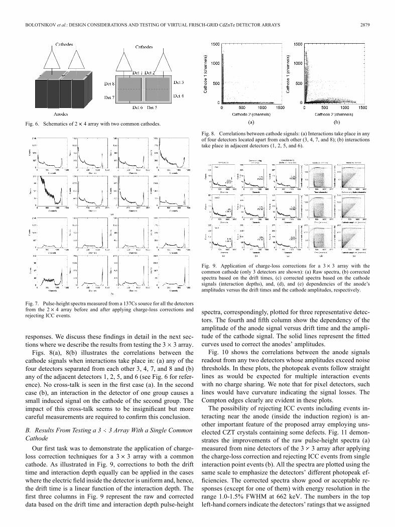
responses. We discuss these findings in detail in the next sec-tions where we describe the results from testing the 3 3 array.Figs. 8(a), 8(b) illustrates the correlations between the
cathode signals when interactions take place in: (a) any of thefour detectors separated from each other 3, 4, 7, and 8 and (b)any of the adjacent detectors 1, 2, 5, and 6 (see Fig. 6 for refer-ence). No cross-talk is seen in the first case (a). In the secondcase (b), an interaction in the detector of one group causes asmall induced signal on the cathode of the second group. Theimpact of this cross-talk seems to be insignificant but morecareful measurements are required to confirm this conclusion.
B. Results From Testing a 3 3 Array With a Single CommonCathode
Our first task was to demonstrate the application of charge-loss correction techniques for a 3 3 array with a commoncathode. As illustrated in Fig. 9, corrections to both the drifttime and interaction depth equally can be applied in the caseswhere the electric field inside the detector is uniform and, hence,the drift time is a linear function of the interaction depth. Thefirst three columns in Fig. 9 represent the raw and correcteddata based on the drift time and interaction depth pulse-height
Fig. 8. Correlations between cathode signals: (a) Interactions take place in anyof four detectors located apart from each other (3, 4, 7, and 8); (b) interactionstake place in adjacent detectors (1, 2, 5, and 6).
Fig. 9. Application of charge-loss corrections for a 3 3 array with thecommon cathode (only 3 detectors are shown): (a) Raw spectra, (b) correctedspectra based on the drift times, (c) corrected spectra based on the cathodesignals (interaction depths), and, (d), and (e) dependencies of the anode’samplitudes versus the drift times and the cathode amplitudes, respectively.
spectra, correspondingly, plotted for three representative detec-tors. The fourth and fifth column show the dependency of theamplitude of the anode signal versus drift time and the ampli-tude of the cathode signal. The solid lines represent the fittedcurves used to correct the anodes’ amplitudes.Fig. 10 shows the correlations between the anode signals
readout from any two detectors whose amplitudes exceed noisethresholds. In these plots, the photopeak events follow straightlines as would be expected for multiple interaction eventswith no charge sharing. We note that for pixel detectors, suchlines would have curvature indicating the signal losses. TheCompton edges clearly are evident in these plots.The possibility of rejecting ICC events including events in-
teracting near the anode (inside the induction region) is an-other important feature of the proposed array employing uns-elected CZT crystals containing some defects. Fig. 11 demon-strates the improvements of the raw pulse-height spectra (a)measured from nine detectors of the 3 3 array after applyingthe charge-loss correction and rejecting ICC events from singleinteraction point events (b). All the spectra are plotted using thesame scale to emphasize the detectors’ different photopeak ef-ficiencies. The corrected spectra show good or acceptable re-sponses (except for one of them) with energy resolution in therange 1.0-1.5% FWHM at 662 keV. The numbers in the topleft-hand corners indicate the detectors’ ratings that we assigned

2880 IEEE TRANSACTIONS ON NUCLEAR SCIENCE, VOL. 60, NO. 4, AUGUST 2013
Fig. 10. Correlations between the anode signals readout from a particulardetectors (vertical axis) and other detectors (horizontal axis) from the 3 3array in which the amplitudes exceed the noise thresholds.
based on their spectral resolution and relative photo-peak effi-ciency. In fact, all spectra look similarly when normalized to thesame height of the photopeaks as illustrated in Fig. 12, but thedetectors have different photo-peak efficiencies; the numbers inthe top left corners indicate the relative number of events underthe photopeaks in percentages of the number found for the bestdetector. The reduction in photopeak events is caused by de-fects in the crystal that “move” ICC events from a photopeakarea into the Compton continuum. Such events can be identifiedand rejected from the pulse-height spectra, so peak-to-Comptonratios stay the same for all detectors. In other words, we effec-tively reduce the detectors’ sensitive volumes by vetoing thedefective regions inside which otherwise contribute to the con-tinuous background. On the other hand, as seen in Fig. 12, thepulse-height spectra plotted before (top lines) and after rejec-tion (bottom lines) have the same heights meaning the rejectionaffects ICC events only.The rejection of ICC events allows us to employ practically
every detector (without compromising an overall array’s per-formance) as long as it provides an acceptable energy resolu-tion even though only a fraction of the crystal is actually used.The array’s effective area can be maintained by selecting detec-tors with smaller fractions of defective regions or using a largernumber of less expensive and easily available detectors; it is atradeoff between the cost and effective area.The feasibility of employing the ICC events algorithm was
demonstrated previously for single interaction point-events [1].Here, we validated the algorithm for single- and multiple-inter-action point events taking place in two or more detectors. Forcompleteness, first we illustrate the rejection algorithm in thecase of single-interaction point events.The first column in Fig. 13 shows the pulse-height spectra
from the source after the charge-loss correction forthree representative detectors. The second and third columns,
Fig. 11. Improvements of the raw pulse-height spectra (a) measured fromnine detectors of the 3 3 array after applying the charge-loss correction andrejecting ICC events from single-interaction point events (b). All the spectraare plotted using the same scale to emphasize the detectors’ different photopeakefficiencies. The numbers in the top left corners indicate the detectors’ ratingsthat we assigned based on their relative photoefficiency.
respectively, show spectra containing only accepted and re-jected events. The last column contains scattered plots of allevents in coordinates: Ratio of cathode to anode, ,versus drift times, . As is evident, the majority of the events(dots) concentrate along the curves whose shapes slightly varyfrom one detector to another. These curves, which we call thecorrelation functions, are evaluated by selecting the photoab-sorption events that are not affected by the crystal’s defects,and fitting their distributions with spline functions (the solidlines going in the middle of the dots distributions in Fig. 13).Two parallel lines represent the wide acceptanceintervals; all events outside these intervals were rejected. As

BOLOTNIKOV et al.: DESIGN CONSIDERATIONS AND TESTING OF VIRTUAL FRISCH-GRID CdZnTe DETECTOR ARRAYS 2881
Fig. 12. Pulse-height spectra from nine detectors of the 3 3 array plottedbefore and after rejecting ICC events. The top lines represent spectra beforerejecting.
Fig. 13. Illustration of the ICC events-rejection algorithm. The first columnshows the pulse-height spectra from the source after the charge-losscorrection for three representative detectors. The second and third columns,respectively, show the spectra containing only accepted and rejected events. Thelast column contains scatter plots of all events in coordinates: Ratio of cathodeto anode, , versus drift times, .
seen, the majority of the rejected events are from the Comptoncontinuum region while the photopeaks remain uncut.The same correlation functions, , also can be used to reject
the ICC events over the entire energy range starting from verylow energies. Fig. 14 shows similar plots as in Fig. 13 but forthe events generated by the low-energy photons from thesource. Again, as previously, we illustrate the results only fromthree detectors.As is evident, events unaffected by the crystal defects follow
the same correlation curves used in the previous case (Fig. 13).Also apparent are the small event losses from the low-energyphotopeaks, . Thus, in the case of the low-energygamma-lines, we need to modify the algorithm.
Fig. 14. Same distributions as in Fig. 13 but plotted for the low-energy gammarays from the source.
Fig. 15. Same distributions as in Figs. 13 but plotted for multiple interaction-point events: (a) two points of interactions; (b) three points of interactions.
For events with multiple interaction points, the adjusted ratio,must be used instead of [12]:
(2)

2882 IEEE TRANSACTIONS ON NUCLEAR SCIENCE, VOL. 60, NO. 4, AUGUST 2013
where is the correlation function of the single-interactionpoint event evaluated for each of the detectors, while andstand for the amplitudes measured from the detector and thecathode. Figs. 15(a) and 15(b), respectively, show pulse-heightspectra similar to those in Figs. 13 and 14 but plotted for two(a) and three (b) interaction-point events. As follows from theseplots, the algorithm works well for multiple interaction pointevents. We note that the rejection algorithm also should be ap-plicable for pixelated detectors.
IV. CONCLUSIONS
We validated our design for arrays of virtual Frisch-grid de-tectors and tested the performance for 2 2, 2 4 and 3 3arrays with common cathodes.The arrays were tested with the currently existing readout
system based on the H3D ASIC, which provides informationon the amplitude and timing of interaction events. A new ASICoptimized for the array is currently under development. It willretain the same functionality to provide both the amplitudeand timing information as the original H3D ASIC. Amplitudeand timing information are critical for the detector’s responsecorrections and achieving the best performance from currentlyavailable CZT crystals.The key elements of the array design are simplicity and the
ability to easily replace individual detectors in the array. Forthis reason we used Cu-Be spring-loaded contacts (instead ofusing conductive epoxy) to provide electrical connections forthe cathodes, anodes and shielding electrodes.We also validated the algorithm for rejecting incomplete
charge-collection events for single- and multiple interaction-point events, which will allow for additional improvements ofthe array’s spectral response.
REFERENCES[1] A. E. Bolotnikov, G. S. Camarda, Y. Cui, G. D. Geronimo, J. Fried,
R. Gul, A. Hossain, K. H. Kim, E. Vernon, G. Yang, and R. B.James, “Array of virtual Frisch-grid CZT detectors with commoncathode readout for correcting charge signals and rejecting incompletecharge-collection events,” IEEE Trans. Nucl. Sci., vol. 59, no. 4, pp.1544–1551, Aug. 2012.
[2] J. K. Polack, M. Hirt, J. Sturgess, N. D. Sferrazza, A. E. Bolotnikov, S.Babalola, G. S. Camarda, Y. Cui, S. U. Egarievwe, P. M. Fochuk, R.Gul, A. Hossain, K. Kim, O. V. Kopach, L. Marchini, G. Yang, L. Xu,and R. B. James, “Variation of electric shielding on virtual Frisch-griddetectors,”Nucl. Instrum.Methods Phys. Res. A, vol. 621, pp. 424–430,2010.
[3] A. E. Bolotnikov, N. M. Abdul-Jabbar, S. Babalola, G. S. Camarda,Y. Cui, A. Hossain, E. Jackson, H. Jackson, J. R. James, A. L. Luryi,and R. B. James, “Optimization of virtual Frisch-grid CdZnTe detectordesigns for imaging and spectroscopy of gamma rays,” in Proc. SPIEHard X-Ray and Gamma-Ray Detector Physics VIII, Invited Paper, L.A. Franks, A. Burger, R. B. James, H. B. Barber, F. P. Doty, and H.Roehrig, Eds. Bellingham, WA, USA: SPIE, 2007, vol. 6702.
[4] A. E. Bolotnikov, S. Babalola, G. S. Camarda, Y. Cui, S. U. Egarievwe,P. M. Fochuk, R. Hawrami, A. Hossain, J. R. James, I. J. Nakonechnyj,Y. Ge, and R. B. James, R. B. James, L. A. Franks, and A. Burger,Eds., “Spectral responses of virtual Frisch-grid cdznte detectors andtheir relation to ir microscopy and X-ray diffraction topography data,”in Proc. SPIE Conf. Hard X-Ray, Gamma-Ray and Neutron DetectorPhysics X, 2008, vol. 7079.
[5] A. E. Bolotnikov, S. Babalola, G. S. Camarda, Y. Cui, S. U. Egarievwe,P. M. Fochuk, M. Hirt, A. Hossain, K. Kim, O. V. Kopach, N. D. Sfer-razza, J. Sturgess, K. Polack, G. Yang, and R. B. James, “Characteriza-tion of a 15-mm-long virtual Frisch-grid CZT detector array,” in Proc.Hard X-Ray, Gamma-Ray, and Neutron Detector Physics XI, InvitedPaper, R. B. James, L. A. Franks, and A. Burger, Eds. Bellingham,WA, USA: SPIE, 2009, vol. 7449, pp. 7449–09.
[6] A. E. Bolotnikov, G. S. Camarda, Y. Cui, S. U. Egarievwe, P. M.Fochuk, M. Fuerstnau, R. Gul, A. Hossain, F. Jones, K. Kim, O. V.Kopach, R. Taggart, G. Yang, Z. Ye, L. Xu, and R. B. James, “Array ofvirtual Frisch-grid CZT detectors with common cathode readout andpulse-height correction,” in Proc. Hard X-Ray, Gamma-Ray, and Neu-tron Detector Physics XI, A. Burger, L. A. Franks, and R. B. James,Eds. Bellingham, WA, USA: SPIE, 2010, vol. 7805, 7805-04.
[7] F. Zhang, Z. He, G. F. Knoll, D. K. Wehe, and J. E. Berry, “3D posi-tion sensitive CdZnTe spectrometer performance using third generationVAS/TAT readout electronics,” IEEE Trans. Nucl. Sci., vol. 52, no. 5,pp. 2009–2016, Oct. 2005.
[8] F. Zhang, C. Herman, Z. He, G. D. Geronimo, E. Vernon, and J. Fried,“Characterization of the H3D ASIC readout system and 6.0 cm 3-Dposition sensitive CdZnTe detectors,” IEEE Trans. Nucl. Sci., vol. 59,no. 1, pp. 236–242, Feb.. 2012.
[9] A. E. Bolotnikov, S. Babalola, G. S. Camarda, Y. Cui, R. Gul, S. U.Egarievwe, P. M. Fochuk, M. Fuerstnau, A. Hossain , F. Jones, K. H.Kim, O. V. Kopach, L. Marchini, B. Raghothamachar, R. Taggart, G.Yang, L. Xu, and R. B. James, “Correlations between crystal defectsand performance of CdZnTe detectors,” IEEE Trans. Nucl. Sci., vol.58, no. 4, pp. 1972–1980, Aug. 2011.
[10] D. S. McGregor and R. A. Rojeski, “High-resolution ionization de-tector and array of such detectors,” U.S. Patent 6 175 120, Jan. 16,2001.
[11] G. Montemont, M. Arques, L. Verger, and J. Rustique, “A capacitiveFrisch grid structure for CdZnTe detectors,” IEEE Trans. Nucl. Sci.,vol. 48, no. 3, pp. 278–281, Jun. 2001.
[12] A. E. Bolotnikov, G. S. Camarda, Y. Cui, G. D. Geronimo, J. Fried,R. Gul, A. Hossain, K. Kim, G. Yang, E. Vernon, and R. B. James,“Rejecting incomplete charge-collection events in CdZnTe and othersemiconductor detectors,” Nucl. Instrum. Methods Phys. Res. A, vol.664, pp. 317–323, 2012.
[13] G. D. Geronimo, E. Vernon, K. Ackley, A. Dragone, J. Fried, P.O’Connor, Z. He, C. Herman, and F. Zhang, “Readout ASIC for 3-Dposition-sensitive detectors,” IEEE Trans. Nucl. Sci., vol. 55, no. 3,pp. 1593–1603, Jun. 2008.
[14] E. Vernon, K. Ackley, G. D. Geronimo, J. Fried, P. O’Connor, Z. He,C. Herman, and F. Zhang, “ASIC for high rate 3-D position sensitivedetectors,” IEEE Trans. Nucl. Sci., vol. 57, no. 3, pp. 1536–1542, Jun.2010.
[15] G. S. Camarda, N. M. Abdul-Jabbar, S. Babalola, A. E. Bolotnikov,Y. Cui, A. Hossain, E. Jackson, H. Jackson, J. R. James, A. L. Luryi,M. Groza, A. Burger, and R. B. James, “Characterization and measure-ments of CZT material: Novel techniques and results,” in Proc. SPIEHard X-Ray and Gamma-Ray Detector Physics IX, R. B. James, A.Burger, and L. A. Franks, Eds. Bellingham, WA, USA: SPIE, 2007,vol. 670605.
[16] A. Hossain, A. E. Bolotnikov, G. C. Camarda, Y. Cui, G. Yang, and R.B. James, “Defects in cadmium zinc telluride crystals revealed by etchpit distributions,” J. Cryst. Growth, vol. 310, pp. 4493–4498, 2008.