design challenges of next-generation wireless
TRANSCRIPT

Design Challenges of Next-Generation Wireless Communication SoCs
Teresa MengDepartment of Electrical Engineering
Stanford University

Communication SoC Technologies
Lots of innovations and new ideas in communication signal processing
W-CDMA, DFE, OFDM, antenna beam-forming, MIMO, etc.
What makes an algorithm appropriate for implementation is rapidly changing
Digital computation exponentially improvingComplex analog circuits linearly degrading (?)
Power dissipation has become one of the main showstoppers.
Requires 100’s of GOP’s of processing per device - how to do it at the lowest energy and smallest area???

Energy and Area Efficiency
MACUnit
AddrGen
µP
Prog Mem
Embedded Processor
(ARM)
Direct MappedHardware
EmbeddedFPGA
DSP
Flex
ibili
ty
Area or Power
ReconfigurableProcessors
Factor of 100-1000
1000 MOPS/mW1000 MOPS/mm2
10-100MOPS/mW
0.5-5 MIPS/mW10 MIPS/mm2

The Dream – "Software Radio"
[Schreier, "ADCs and DACs: Marching Towards the Antenna," GIRAFE workshop, ISSCC 2003]

Reality – "Heat-sink Radio"
[Schreier, "ADCs and DACs: Marching Towards the Antenna," GIRAFE workshop, ISSCC 2003]

Today's Analog Circuits
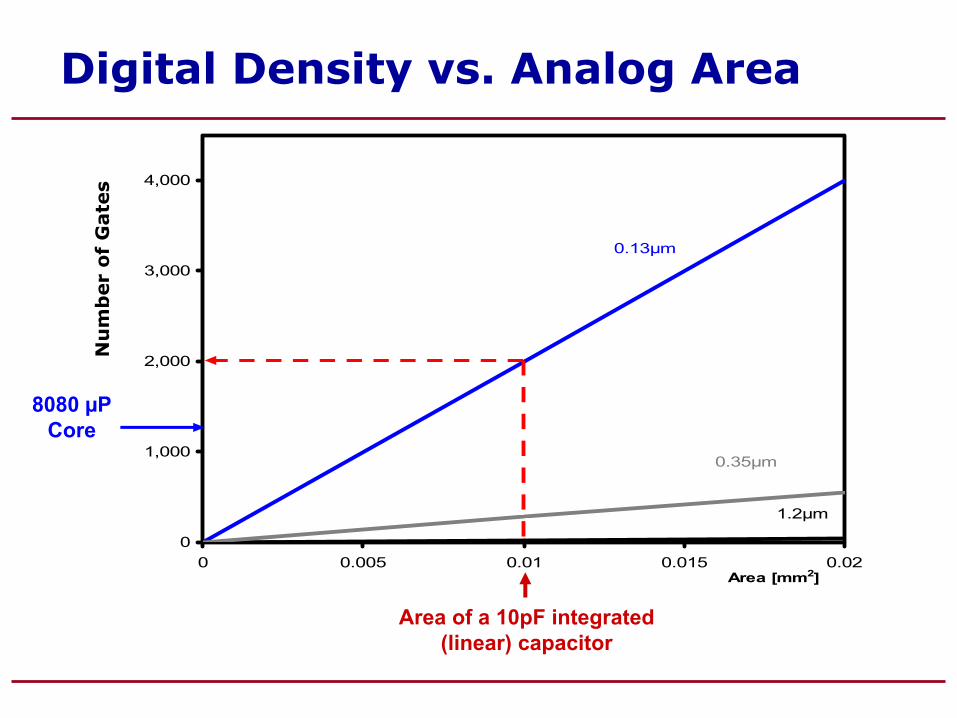
Digital Density vs. Analog Area
0
1,000
2,000
3,000
4,000
0 0.005 0.01 0.015 0.02Area [mm2]
0.13µm
1.2µm
0.35µm
Area of a 10pF integrated (linear) capacitor
8080 µP Core
Nu
mb
er
of
Gate
s

Digital Energy Efficiency
Number of logic gates with same energy as a state-of-the-art B-bit ADC
0
200,000
400,000
600,000
800,000
1,000,000
6 8 10 12 14 16ADC Resolution [B]
0.13µm
1.2µm
0.35µmNu
mb
er
of
Gate
s

Real Life Example: 802.11 a/g
RF Baseband
Rx ~ 300mWTx ~ 1500mW
Digital (50 GOPS, 0.13µm) ~ 50mWADC (2x9b, 80MHz) ~ 200mW

Observations
It is not new to realize that digital signal processing is superior to analog in terms of energy efficiency
What's new is the relative size of the gap between digital and analog capabilities, mostly due to advancements of last 10 years
Necessary paradigm shiftToday: "Let's use some logic gates to correct/calibrate analog circuits"Future: "How many analog transistors dowe really need?"
How can we use digital logic more aggressively to "assist" analog functions, such as ADCs and PAs?

Analog Circuit Challenges
Thermal NoiseSet by supply voltage and capacitanceFundamental
DistortionExacerbated by low supplies & intrinsic device gainTraditional solution: high-gain feedbackNot fundamental
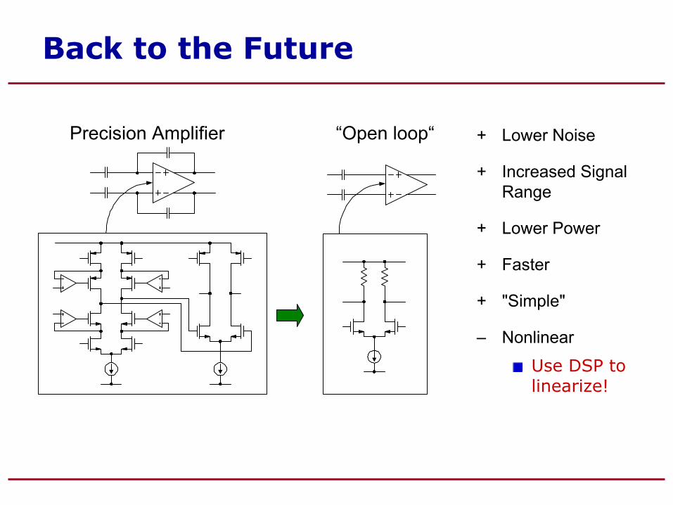
Back to the Future
+ Lower Noise
+ Increased Signal Range
+ Lower Power
+ Faster
+ "Simple"
– Nonlinear
Use DSP to linearize!
“Open loop“Precision Amplifier

Digital Nonlinearity Compensation
SystemID
AnalogNonlinearity
DigitalInverse
Modulation
Dout,corrVin Dout
Parameters
Use system ID to determine optimum post correction
Possible to track variations over time without interrupting normal circuit operation

Example: Pipelined ADC
Σ
A/D D/A-
D
VresVin
STAGE 1 STAGE N-1 STAGE NS/H
R bits
Vin
2R
D=0 D=1
⇒
V res
Vin
(e.g. R=1)
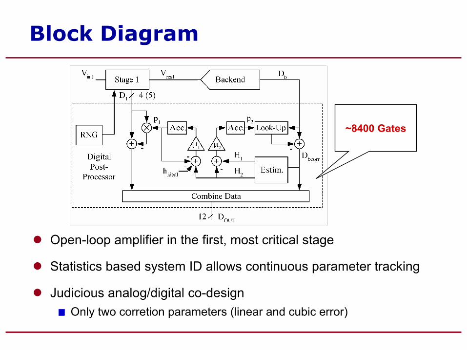
Block Diagram
~8400 Gates
Open-loop amplifier in the first, most critical stage
Statistics based system ID allows continuous parameter tracking
Judicious analog/digital co-designOnly two corretion parameters (linear and cubic error)

Measurement Results
0 1000 2000 3000 4000-1
-0.5
0
0.5
1(b) with calibration
C d
0 1000 2000 3000 4000
-10
0
10
(a) without calibration
Code
INL
[LSB
]
RNG=0RNG=1
0 1000 2000 3000 4000
-10
0
10
(b) with calibration
Code
INL
[LS
B]

Stage 1 Power Breakdown
0
10
20
30
40
50
Pow
er [m
W]
AD9235 This Work
FlashBiasingGmPost-Proc.
-75%
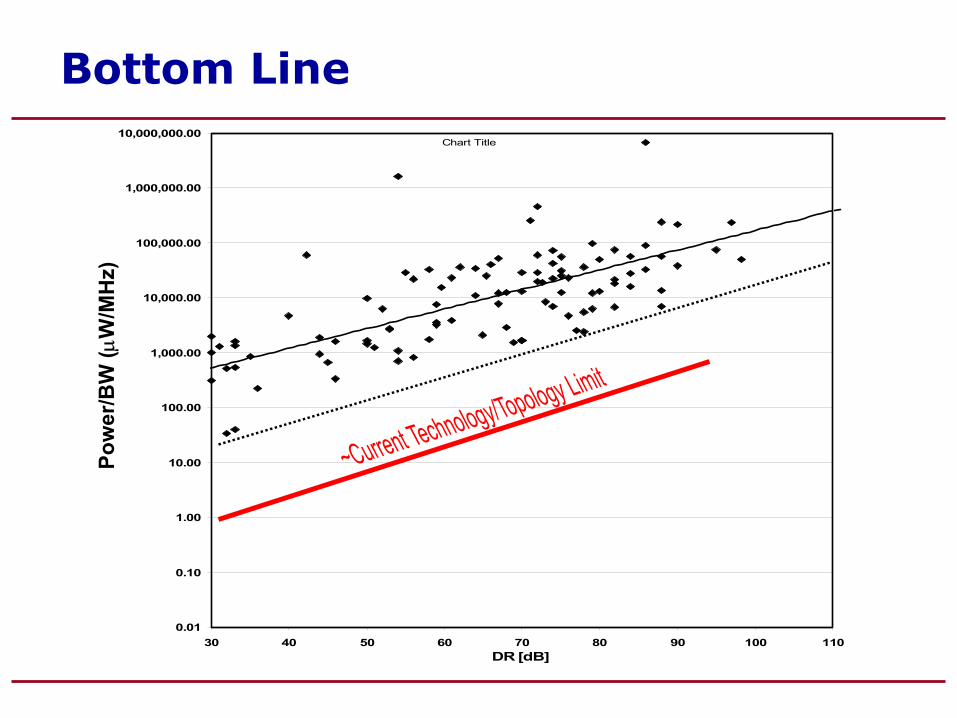
Bottom LineChart Title
0.01
0.10
1.00
10.00
100.00
1,000.00
10,000.00
100,000.00
1,000,000.00
10,000,000.00
30 40 50 60 70 80 90 100 110DR [dB]
Pow
er/B
W (µ
W/M
Hz)

Summary - Digitially Assisted ADCs
Simplified analog circuits are key to improving power efficiency in A/D
Power savings of better than one order of magnitude seem possible
Other benefits of simplistic analog designsIntroduces redundancy, e.g. for yield enhancement
Creates adjustable, massively parallel arrays in small area
Inherently self-calibrating, potentially self-repairingSimplifies testing
Ideal for remote, maintenance free operation, e.g. in remote sensing networks

Digitally Assisted PA Design
Transmitter power efficiency is limited byHigh peak-to-average power ratio (PAR)
Power amplifier (PA) non-linearity
Linear PA design is increasingly difficult
Digital circuit capabilities grow exponentially1 GOPS/mW, 1 GOPS/mm2 in 0.13 µm CMOS
How to achieve maximum power efficiency?

PA Design Example: 802.11a/g
Of 64 the carriers:12 free carriers (in black) on sides and center
48 data carriers (in green) per symbol
4 pilots carriers (in red) per symbol for synchronization
20 MHz
OFDM (52 of 64 carriers used)
BPSK QPSK 16QAM 64QAM

High PAR in Time-domain Signal
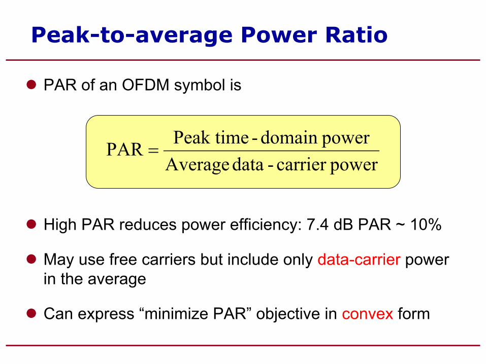
PAR of an OFDM symbol is
High PAR reduces power efficiency: 7.4 dB PAR ~ 10%
May use free carriers but include only data-carrier power in the average
Can express “minimize PAR” objective in convex form
Peak-to-average Power Ratio
powercarrier -data Averagepowerdomain -Peak timePAR =

Convex Optimization
Standard Convex Optimization Problem
Each f(x) is a convex function
The globally optimal solution can be efficiently calculated“The great watershed in optimization isn't between linearity andnonlinearity, but convexity and nonconvexity.”
--R. Rockafellar, SIAM Review, June 1993
n
i
xbAx
mixfxf
R∈
==≤
esin variabl
,,10)(tosubject)(minimize 0
Κ
]1,0[allfor),()1()())1(( ∈−+≤−+ θθθθθ yfxfyxf

Transmitter Constraints
PAR reduction should not change receiver structure

Transmitter Constraints
PAR reduction should not change receiver structure

Transmitter Constraints
Ideal OFDM constellation c, transmitted constellation ĉ
Data carrier Error Vector Magnitude constraintLimit individual EVM
Limit average EVM
Free carrier Spectral Mask constraint
Constraints are convex inequalities
ε≤−∑=
D
i
i
iiii cc
D2ˆ1
Dii iiiicc ,,,,ˆ 21 Κ=≤− ε
iic δ≤ˆ
…

PAR Minimization
PAR objective is convex
Constellation constraints are convex
PAR minimization is a convex problem
Use convex optimization theory to find the signal with MINIMUM PAR that satisfies transmitter EVM
Controlled error vs. random error introduced in the constellation points in frequency domain
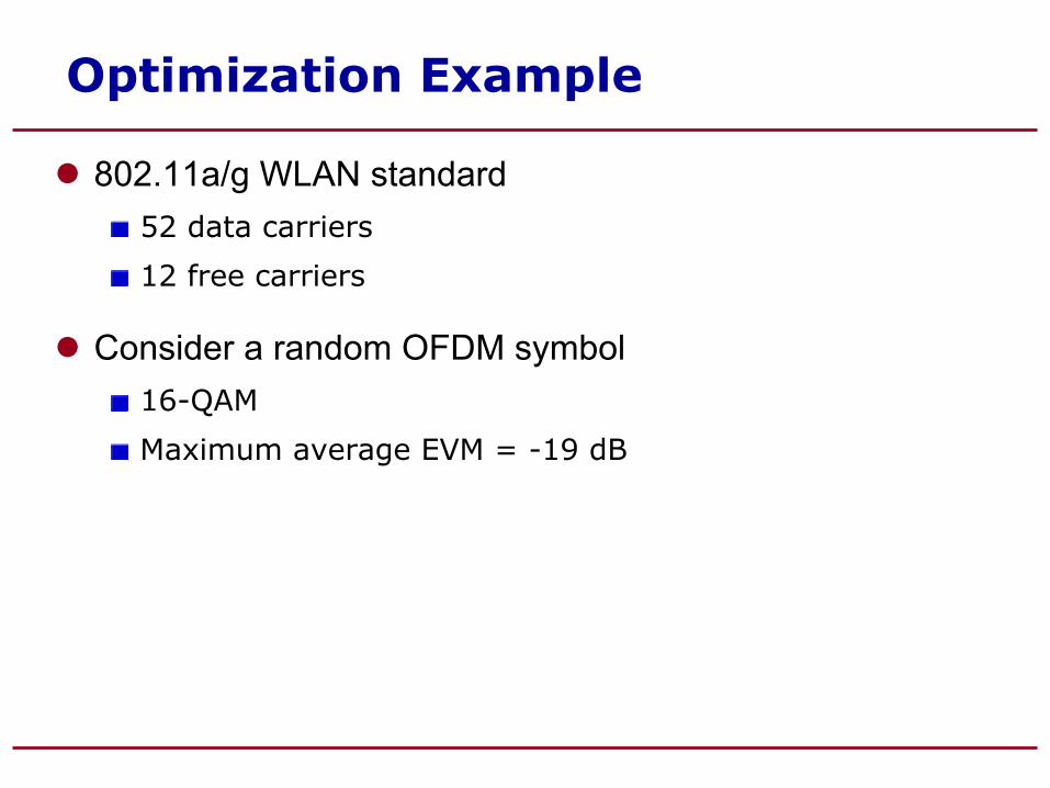
Optimization Example
802.11a/g WLAN standard52 data carriers
12 free carriers
Consider a random OFDM symbol16-QAM
Maximum average EVM = -19 dB

Example: Frequency-domain

Example: Frequency-domain
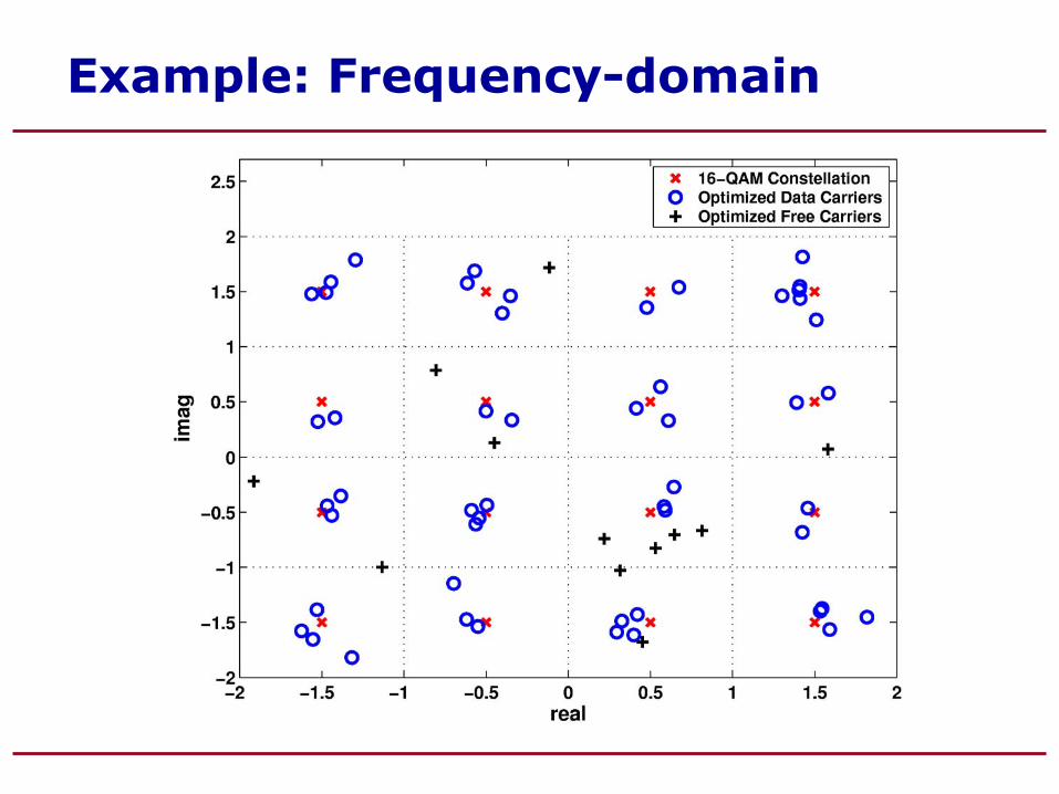
Example: Frequency-domain

Example: Time-domain
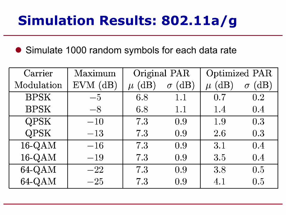
Simulation Results: 802.11a/g
Simulate 1000 random symbols for each data rate

Convex Optimized PA
Achieves globally minimum PAR in OFDM signals
Delivers maximum power efficiency
Establishes performance limits for analyzing existing PAR reduction methods
Is feasible for real-time implementation using modern CMOS technology
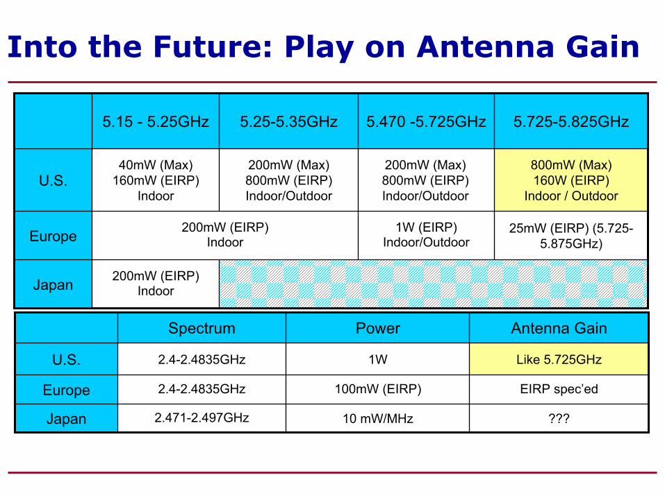
Into the Future: Play on Antenna Gain
200mW (EIRP)IndoorJapan
25mW (EIRP) (5.725-5.875GHz)
1W (EIRP)Indoor/Outdoor
200mW (EIRP)IndoorEurope
800mW (Max)160W (EIRP)
Indoor / Outdoor
200mW (Max)800mW (EIRP)Indoor/Outdoor
40mW (Max)160mW (EIRP)
IndoorU.S.
5.725-5.825GHz5.470 -5.725GHz5.25-5.35GHz5.15 - 5.25GHz
100mW (EIRP)
???10 mW/MHz2.471-2.497GHzJapan
EIRP spec’ed2.4-2.4835GHzEurope
Like 5.725GHz1W2.4-2.4835GHzU.S.
Antenna GainPowerSpectrum
200mW (Max)800mW (EIRP)Indoor/Outdoor

Why is 60 GHz interesting?
Lots of Bandwidth!!!
7 GHz of unlicensed bandwidth in the U.S. and Japan
Reasonable transmit power (0.5W) and high antenna gains are allowed
57 dBm
40 dBm
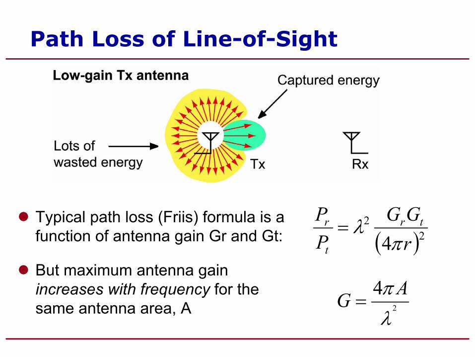
Path Loss of Line-of-Sight
( )22
4 rGG
PP tr
t
r
πλ=
2
4λπ AG =
Typical path loss (Friis) formula is a function of antenna gain Gr and Gt:
But maximum antenna gain increases with frequency for the same antenna area, A

Antenna Gain for Constant Area
22
1rAA
PP tr
t
r
λ=
High carrier frequencies allow higher antenna gain with the same amount of antenna area
There is theoretically 22 dB gain at 60 GHz over 5 GHz with optimal antenna design

Future SoCs: MIMO on a Chip
Goal: Multiple transmit/receive chains on a single chip
ChallengesComplexity, crosstalk
AdvantagesRange extension
Capacity increase
Cost reduction by SoC
D/A
D/AD/A
D/AD/A
1
2
N
1
2
N
A/D
A/DA/D
A/DA/D
1
2
N
1
2
N
Parallel RF Front-End
AdaptiveBeam-Forming
andCoherent
Combining
OFDM Multi-Carrier
Tx/Rx

SoC Complexity and Feasibility
Range extension determined by 800mW x 200 ~ 160 W!
Capacity increase determined by the amount of diversity7 channels, 3 sectors, 20 transceiver chains per sector30Mbps for 20Mhz channel at 5Ghz, 1Gbps for 1Ghz channel at 60GhzTotal capacity 7*3*(20/2)*30Mbps = 6.3 Gbps!
Computation and silicon area requirementsComputation: 50 GOPS per transceiver, 7*3*20*50*2 GOPS = 42 TOPSDigital silicon: 42,000 GOPS/1 GOPS/mm2/4 ~ 10x10 cm2
Analog silicon: 7*3*20*10 mm2 ~ 7x7 cm2
At 60GHz, data rate is increased by another factor of 30.

Conclusions
With highly energy efficient digital technology, we must challenge basic analog design techniques.
Integration capability is crucial to future complex wireless system design.
CMOS is able to exploit the unlicensed 60 GHz band with 7 GHz of bandwidth. However, it will take a new design and modeling methodology.
Key to success: Interdisciplinary approach with device modeling, analog circuit design and DSP algorithms.

Thank you