design and verification of a dfi-axi ddr4 memory phy
TRANSCRIPT

Rochester Institute of Technology Rochester Institute of Technology
RIT Scholar Works RIT Scholar Works
Theses
8-2019
Design and Verification of a DFI-AXI DDR4 Memory PHY Bridge Design and Verification of a DFI-AXI DDR4 Memory PHY Bridge
Suitable for FPGA Based RTL Emulation and Prototyping Suitable for FPGA Based RTL Emulation and Prototyping
Pallavi Avinash Mayekar [email protected]
Follow this and additional works at: https://scholarworks.rit.edu/theses
Recommended Citation Recommended Citation Mayekar, Pallavi Avinash, "Design and Verification of a DFI-AXI DDR4 Memory PHY Bridge Suitable for FPGA Based RTL Emulation and Prototyping" (2019). Thesis. Rochester Institute of Technology. Accessed from
This Thesis is brought to you for free and open access by RIT Scholar Works. It has been accepted for inclusion in Theses by an authorized administrator of RIT Scholar Works. For more information, please contact [email protected].

DESIGN AND VERIFICATION OF A
DFI-AXI DDR4 MEMORY PHY BRIDGE
SUITABLE FOR FPGA BASED
RTL EMULATION AND PROTOTYPING
PALLAVI AVINASH MAYEKAR
DESIGN AND VERIFICATION OF A DFI-AXI DDR4 MEMORY PHY BRIDGE
SUITABLE FOR FPGA BASED RTL EMULATION AND PROTOTYPING
BY
PALLAVI AVINASH MAYEKAR
A THESIS
SUBMITTED IN PARTIAL FULFILLMENT
OF THE REQUIREMENTS FOR THE DEGREE OF
MASTER OF SCIENCE
IN ELECTRICAL ENGINEERING
DEPARTMENT OF ELECTRICAL AND MICROELECTRONIC ENGINEERING
KATE GLEASON COLLEGE OF ENGINEERING
ROCHESTER INSTITUTE OF TECHNOLOGY
ROCHESTER, NEW YORK
AUGUST, 2019

DESIGN AND VERIFICATION OF A DFI-AXI DDR4 MEMORY PHY BRIDGE
SUITABLE FOR FPGA BASED RTL EMULATION AND PROTOTYPING
PALLAVI AVINASH MAYEKAR
Committee Approval:We, the undersigned committee members, certify that Pallavi Avinash Mayekar hascompleted the requirements for the Master of Science degree in Electrical Engineering.
Mr. Mark A. Indovina, Graduate Research Advisor DateSenior Lecturer, Department of Electrical and Microelectronic Engineering
Dr. Dorin Patru DateAssociate Professor, Department of Electrical and Microelectronic Engineering
Dr. Dan Phillips DateAssociate Professor, Department of Electrical and Microelectronic Engineering
Dr. Sohail Dianat, Department Head DateProfessor, Department of Electrical and Microelectronic Engineering

I would like to dedicate this work to my family, my grandparents, my father Avinash, my
mother Anjali, my sister Pooja, my brother Vaibhav, and friends for their unconditional love and
support during my thesis.

Declaration
I hereby declare that except where specific reference is made to the work of others, that all
content of this Graduate Thesis is original and have not been submitted in whole or in part for
consideration for any other degree or qualification in this, or any other University. This Graduate
Thesis is the result of my own work and includes nothing which is the outcome of work done in
collaboration, except where specifically indicated in the text.
Pallavi Avinash Mayekar
August, 2019

Acknowledgements
I am very grateful to my advisor Professor Mark A. Indovina, for providing guidance and feed-
back during these past three years. Mark is one smartest people I know who also makes learning
fun. He is my best role model for an engineer, teacher, and mentor. Mark was the reason why I
decided to go and pursue a career in Digital design and verification. Thank you for all the sup-
port and encouragement. I would like to thank Chris Browy and Chilai Huang of Avery Design
Systems as the motivation behind this project, for their helpful suggestions, and for providing
access, and licenses to the Avery VIP discussed in this paper. Chris was a primary source for
getting certain specification related questions answered. I would also like to thank the members
of my thesis committee, Dr. Dorin Patru, and Dr. Dan Phillips for their feedback, helpful career
advice and general suggestions. I also thank all professors whose knowledge and experience
helped me guide in my pursuit of a Master’s Degree at Rochester Institute of Technology.

Abstract
System on chip (SoC) designers today are emphasizing on a process which can ensure robust
silicon at the first tape-out. Given the complexity of modern SoC chips, there is compelling
need to have suitable run time software, such at the Linux kernel and necessary drivers available
once prototype silicon is available. Emulation and FPGA prototyping systems are exemplary
platforms to run the tests for designs, are naturally efficient and perform well, and enable early
software development. While useful, one needs to keep in mind that emulation and FPGA pro-
totyping systems do not run at full silicon speed. In fact, the SoC target ported to the FPGA
might achieve a clock speed less than 10 MHz. While still very useful for testing and software
development, this low operating speed creates challenges for connecting to external devices such
as DDR SDRAM. In this paper, the DDR-PHY INTERFACE (DFI) to Advanced eXtensible In-
terface (AXI) Bridge is designed to support a DDR4 memory sub-system design. This bridge
module is developed based on the DDR PHY Interface version 5.0 specification, and once imple-
mented in an FPGA, it transfers command information and data between the SoC DDR Memory
controller being prototypes, across the AXI bus to an FPGA specific memory controller con-
nected to a DDR SDRAM or other physical memory external to the FPGA. This bridge module
enables multi-communication with the design under test (DUT) with a synthesizable SCE-MI
based infrastructure between the bridge and logic simulator. SCE-MI provides a direct mecha-
nism to inject the specific traffic, and monitor performance of the DFI-AXI DDR4 Memory PHY
Bridge. Both Emulation and FPGA prototyping platforms can use this design and its testbench.

Contents
Contents v
List of Figures ix
List of Tables xi
Glossary xiv
1 Introduction 1
1.1 Research Goals . . . . . . . . . . . . . . . . . . . . . . . . . . . . . . . . . . . 4
1.2 Contributions . . . . . . . . . . . . . . . . . . . . . . . . . . . . . . . . . . . . 4
1.3 Thesis Organization . . . . . . . . . . . . . . . . . . . . . . . . . . . . . . . . . 5
2 Background Research 6
2.1 DDR memory sub-system . . . . . . . . . . . . . . . . . . . . . . . . . . . . . . 8
2.1.1 DDR Memory . . . . . . . . . . . . . . . . . . . . . . . . . . . . . . . 10
2.1.2 DDR Memory Controller . . . . . . . . . . . . . . . . . . . . . . . . . . 15
2.1.3 DDR4 PHY . . . . . . . . . . . . . . . . . . . . . . . . . . . . . . . . . 16
2.2 AXI Protocol . . . . . . . . . . . . . . . . . . . . . . . . . . . . . . . . . . . . 16
2.3 SystemVerilog for Verification . . . . . . . . . . . . . . . . . . . . . . . . . . . 19

Contents vi
2.4 UVM for Verification . . . . . . . . . . . . . . . . . . . . . . . . . . . . . . . . 22
3 Architecture Overview 25
3.1 SoC (DUT) Memory Controller . . . . . . . . . . . . . . . . . . . . . . . . . . 26
3.2 DFI . . . . . . . . . . . . . . . . . . . . . . . . . . . . . . . . . . . . . . . . . 26
3.2.1 Interface Group . . . . . . . . . . . . . . . . . . . . . . . . . . . . . . . 27
3.2.1.1 Command Interface . . . . . . . . . . . . . . . . . . . . . . . 27
3.2.1.2 Write Data Interface . . . . . . . . . . . . . . . . . . . . . . . 32
3.2.1.3 Read Data Interface . . . . . . . . . . . . . . . . . . . . . . . 32
3.2.1.4 Update Interface . . . . . . . . . . . . . . . . . . . . . . . . . 38
3.2.1.5 Status Interface . . . . . . . . . . . . . . . . . . . . . . . . . 43
3.2.1.6 Low Power Control Interface . . . . . . . . . . . . . . . . . . 47
3.2.1.7 Error Interface . . . . . . . . . . . . . . . . . . . . . . . . . . 50
3.2.1.8 PHY Master Interface . . . . . . . . . . . . . . . . . . . . . . 52
3.2.1.9 Disconnect Protocol . . . . . . . . . . . . . . . . . . . . . . . 56
3.2.1.10 2N Mode Interface . . . . . . . . . . . . . . . . . . . . . . . . 56
3.2.1.11 MC to PHY Message Interface . . . . . . . . . . . . . . . . . 57
3.2.1.12 WCK Control Interface . . . . . . . . . . . . . . . . . . . . . 57
3.3 DFI-AXI DDR4 Memory PHY Bridge . . . . . . . . . . . . . . . . . . . . . . . 59
3.3.1 Command Transaction Unit . . . . . . . . . . . . . . . . . . . . . . . . 59
3.3.1.1 Initialization Unit . . . . . . . . . . . . . . . . . . . . . . . . 59
3.3.1.2 Control Unit . . . . . . . . . . . . . . . . . . . . . . . . . . . 60
3.3.1.3 Decode Command Unit . . . . . . . . . . . . . . . . . . . . . 60
3.3.2 Write Transaction Unit . . . . . . . . . . . . . . . . . . . . . . . . . . . 61
3.3.2.1 Write FSM . . . . . . . . . . . . . . . . . . . . . . . . . . . 61

Contents vii
3.3.2.2 Write FIFO . . . . . . . . . . . . . . . . . . . . . . . . . . . 62
3.3.3 Read Transaction Unit . . . . . . . . . . . . . . . . . . . . . . . . . . . 63
3.3.3.1 Read FSM . . . . . . . . . . . . . . . . . . . . . . . . . . . . 63
3.3.3.2 Read FIFO . . . . . . . . . . . . . . . . . . . . . . . . . . . 65
3.3.4 Interactions Unit . . . . . . . . . . . . . . . . . . . . . . . . . . . . . . 65
3.3.4.1 DFI interactions FSM . . . . . . . . . . . . . . . . . . . . . . 65
3.3.4.2 SCE-MI Controller . . . . . . . . . . . . . . . . . . . . . . . 68
3.4 SCE-MI . . . . . . . . . . . . . . . . . . . . . . . . . . . . . . . . . . . . . . . 68
3.5 AXI Master transactor . . . . . . . . . . . . . . . . . . . . . . . . . . . . . . . 69
3.5.1 AXI Write Channel . . . . . . . . . . . . . . . . . . . . . . . . . . . . . 69
3.5.2 AXI Read Channel . . . . . . . . . . . . . . . . . . . . . . . . . . . . . 74
3.6 AXI . . . . . . . . . . . . . . . . . . . . . . . . . . . . . . . . . . . . . . . . . 78
3.6.1 Write Address Channel . . . . . . . . . . . . . . . . . . . . . . . . . . . 78
3.6.2 Write Data Channel . . . . . . . . . . . . . . . . . . . . . . . . . . . . 79
3.6.3 Write Response Channel . . . . . . . . . . . . . . . . . . . . . . . . . . 79
3.6.4 Read Address Channel . . . . . . . . . . . . . . . . . . . . . . . . . . . 80
3.6.5 Read Response Channel . . . . . . . . . . . . . . . . . . . . . . . . . . 81
4 Verification Environment 82
4.1 Testbench Architecture . . . . . . . . . . . . . . . . . . . . . . . . . . . . . . . 82
4.1.1 Testbench Architecture with DDR Memory Subsystem . . . . . . . . . . 82
4.1.2 Testbench Architecture with AXI Slave . . . . . . . . . . . . . . . . . . 84
4.2 Coverage . . . . . . . . . . . . . . . . . . . . . . . . . . . . . . . . . . . . . . 85
4.3 Assertions . . . . . . . . . . . . . . . . . . . . . . . . . . . . . . . . . . . . . . 85

Contents viii
5 Results and Discussion 86
5.1 Testcase Scenario . . . . . . . . . . . . . . . . . . . . . . . . . . . . . . . . . . 86
5.2 Simulation Results . . . . . . . . . . . . . . . . . . . . . . . . . . . . . . . . . 87
5.3 Coverage Results . . . . . . . . . . . . . . . . . . . . . . . . . . . . . . . . . . 93
6 Conclusion 94
6.1 Futurework . . . . . . . . . . . . . . . . . . . . . . . . . . . . . . . . . . . . . 95
References 96

List of Figures
2.1 DRAM Top Level Diagram . . . . . . . . . . . . . . . . . . . . . . . . . . . . . 7
2.2 Decoding Row and Column Address Fields [1] . . . . . . . . . . . . . . . . . . 8
2.3 DDR Memory Sub-system [2] . . . . . . . . . . . . . . . . . . . . . . . . . . . 9
2.4 State Diagram of DDR4 [3] . . . . . . . . . . . . . . . . . . . . . . . . . . . . . 13
2.5 Block diagram of Memory Controller [4] . . . . . . . . . . . . . . . . . . . . . 14
2.6 Write Transaction Channel Architecture . . . . . . . . . . . . . . . . . . . . . . 18
2.7 Read Transaction Channel Architecture . . . . . . . . . . . . . . . . . . . . . . 18
2.8 Standard OOP Testbench Architecture . . . . . . . . . . . . . . . . . . . . . . . 23
3.1 System-level Architecture of Memory Sub-system . . . . . . . . . . . . . . . . . 25
3.2 Block diagram of DDR PHY Interface signals [5] . . . . . . . . . . . . . . . . . 28
3.3 Write Finite State Machine . . . . . . . . . . . . . . . . . . . . . . . . . . . . . 62
3.4 Read Finite State Machine . . . . . . . . . . . . . . . . . . . . . . . . . . . . . 64
3.5 DFI Interactions State Machine . . . . . . . . . . . . . . . . . . . . . . . . . . . 66
3.6 AXI Write Channel Master Transactor Block Diagram [6] . . . . . . . . . . . . 70
3.7 AXI Read Channel Master Transactor Block Diagram [6] . . . . . . . . . . . . . 74
3.8 AXI Write Address Message . . . . . . . . . . . . . . . . . . . . . . . . . . . . 78
3.9 AXI Write Data Message . . . . . . . . . . . . . . . . . . . . . . . . . . . . . . 79
List of Figures x
3.10 AXI Write Response Message . . . . . . . . . . . . . . . . . . . . . . . . . . . 80
3.11 AXI Read Address Message . . . . . . . . . . . . . . . . . . . . . . . . . . . . 80
3.12 AXI Read Response Message . . . . . . . . . . . . . . . . . . . . . . . . . . . . 81
4.1 Top-level Verification Architecture with DDR4 Memory Subsystem . . . . . . . 83
4.2 Top-level Verification Architecture with AXI Slave VIP . . . . . . . . . . . . . . 84
5.1 Write Interface Signal Transaction with Burst of 8 . . . . . . . . . . . . . . . . . 86
5.2 Read Interface Signal Transaction with with Burst of 8 . . . . . . . . . . . . . . 87
5.3 Write Address Transaction with 2 Independent Writes . . . . . . . . . . . . . . . 88
5.4 Write Data Transaction with Burst of 8 . . . . . . . . . . . . . . . . . . . . . . . 88
5.5 Read Address Transaction With 2 Independent Reads . . . . . . . . . . . . . . . 89
5.6 Read Data Transaction with Burst of 8 . . . . . . . . . . . . . . . . . . . . . . . 89
5.7 Write Data Interface Simulation Waveforms . . . . . . . . . . . . . . . . . . . . 91
5.8 Read Data Interface Simulation Waveforms . . . . . . . . . . . . . . . . . . . . 92
5.9 IMC Environment Coverage Report . . . . . . . . . . . . . . . . . . . . . . . . 93
List of Tables
2.1 DRAM Input And Output Pins [3, 7] . . . . . . . . . . . . . . . . . . . . . . . . 7
2.2 Comparing DDR family [8] . . . . . . . . . . . . . . . . . . . . . . . . . . . . . 11
2.3 DDR Command table [3, 5, 7, 9] . . . . . . . . . . . . . . . . . . . . . . . . . . 14
2.4 OOP Testbench Components [10] . . . . . . . . . . . . . . . . . . . . . . . . . 19
2.4 OOP Testbench Components [10] . . . . . . . . . . . . . . . . . . . . . . . . . 20
2.4 OOP Testbench Components [10] . . . . . . . . . . . . . . . . . . . . . . . . . 21
2.4 OOP Testbench Components [10] . . . . . . . . . . . . . . . . . . . . . . . . . 22
3.1 Command Interface Signals [5] . . . . . . . . . . . . . . . . . . . . . . . . . . . 29
3.1 Command Interface Signals [5] . . . . . . . . . . . . . . . . . . . . . . . . . . . 30
3.1 Command Interface Signals [5] . . . . . . . . . . . . . . . . . . . . . . . . . . . 31
3.1 Command Interface Signals [5] . . . . . . . . . . . . . . . . . . . . . . . . . . . 32
3.2 Command Interface Timing Parameters [5] . . . . . . . . . . . . . . . . . . . . 33
3.4 Write Data Interface Signals [5] . . . . . . . . . . . . . . . . . . . . . . . . . . 34
3.5 Write Data Interface Timing Parameters [5] . . . . . . . . . . . . . . . . . . . . 35
3.6 Read Data Interface Signals [5] . . . . . . . . . . . . . . . . . . . . . . . . . . . 36
3.7 Read Data Interface Timing Parameters [5] . . . . . . . . . . . . . . . . . . . . 37
3.8 Update Interface Signals [5] . . . . . . . . . . . . . . . . . . . . . . . . . . . . 38

List of Tables xii
3.8 Update Interface Signals [5] . . . . . . . . . . . . . . . . . . . . . . . . . . . . 39
3.8 Update Interface Signals [5] . . . . . . . . . . . . . . . . . . . . . . . . . . . . 40
3.8 Update Interface Signals [5] . . . . . . . . . . . . . . . . . . . . . . . . . . . . 41
3.9 Update Interface Timing Parameters [5] . . . . . . . . . . . . . . . . . . . . . . 42
3.10 Status Interface Signals [5] . . . . . . . . . . . . . . . . . . . . . . . . . . . . . 43
3.10 Status Interface Signals [5] . . . . . . . . . . . . . . . . . . . . . . . . . . . . . 44
3.10 Status Interface Signals [5] . . . . . . . . . . . . . . . . . . . . . . . . . . . . . 45
3.11 Status Interface Timing Parameters [5] . . . . . . . . . . . . . . . . . . . . . . . 46
3.12 Low Power Control Interface Signals [5] . . . . . . . . . . . . . . . . . . . . . . 47
3.12 Low Power Control Interface Signals [5] . . . . . . . . . . . . . . . . . . . . . . 48
3.12 Low Power Control Interface Signals [5] . . . . . . . . . . . . . . . . . . . . . . 49
3.12 Low Power Control Interface Signals [5] . . . . . . . . . . . . . . . . . . . . . . 50
3.13 Low Power Control Interface Timing Parameters [5] . . . . . . . . . . . . . . . . 51
3.14 Error Interface Signals [5] . . . . . . . . . . . . . . . . . . . . . . . . . . . . . 51
3.15 Error Interface Timing Parameters [5] . . . . . . . . . . . . . . . . . . . . . . . 51
3.16 PHY Master Interface Signals [5] . . . . . . . . . . . . . . . . . . . . . . . . . . 52
3.16 PHY Master Interface Signals [5] . . . . . . . . . . . . . . . . . . . . . . . . . . 53
3.16 PHY Master Interface Signals [5] . . . . . . . . . . . . . . . . . . . . . . . . . . 54
3.17 PHY Master Interface Timing Parameters [5] . . . . . . . . . . . . . . . . . . . 55
3.18 Disconnect Protocol [5] . . . . . . . . . . . . . . . . . . . . . . . . . . . . . . . 56
3.19 Disconnect Protocol Timing Parameters [5] . . . . . . . . . . . . . . . . . . . . 56
3.20 2N Mode Interface Signals [5] . . . . . . . . . . . . . . . . . . . . . . . . . . . 56
3.21 2N Mode Interface Timing Parameters [5] . . . . . . . . . . . . . . . . . . . . . 57
3.22 MC to PHY Message Interface Signals [5] . . . . . . . . . . . . . . . . . . . . . 57
3.23 MC to PHY Message Interface Timing Parameters [5] . . . . . . . . . . . . . . . 58

List of Tables xiii
3.24 WCK Control Interface Signals [5] . . . . . . . . . . . . . . . . . . . . . . . . . 58
3.25 WCK Control Interface Timing Parameters [5] . . . . . . . . . . . . . . . . . . . 58
3.26 Truthtable of DFI Interaction Signals . . . . . . . . . . . . . . . . . . . . . . . . 67
3.27 Write Channel SFR Registers [6] . . . . . . . . . . . . . . . . . . . . . . . . . . 73
3.28 Read Channel SFR Registers [6] . . . . . . . . . . . . . . . . . . . . . . . . . . 77
5.1 Frequency Mode . . . . . . . . . . . . . . . . . . . . . . . . . . . . . . . . . . 87
5.2 Write Requests . . . . . . . . . . . . . . . . . . . . . . . . . . . . . . . . . . . 87
5.3 Coverage Analysis . . . . . . . . . . . . . . . . . . . . . . . . . . . . . . . . . 93

Glossary
Acronyms
AMBA Advanced Microcontroller Bus Architecture
ARM Advanced RISC Machine
ASIC Application-specific Integrated Circuit
AXI Advanced eXtensible Interface
CAS Column Address Strobe
CDC Clock Domain Crossing
DDR Double data rate
DFI DDR-PHY Interface
DUT Device Under Test
FPGA Field Programmable Gate Array
HDL Hardware Description Language
IC Integrated Circuit

Glossary xv
IMC Integrated Metric Center
JEDEC Joint Electron Device Engineering Council (JEDEC) Solid State Technology As-
sociation
MC Memory Controller
OOP Object-oriented Programming
RAS Row Address Strobe
RTL Register-Transfer Level
SDRAM Synchronus Dynamic Random-Access Memory
SoC System on Chip
TLM Transaction Level Modeling
UVM Universal Verification Methodology
VIP Verification Intellectual Property
VLSI Very Large Scale Integration
Chapter 1
Introduction
Modern SoC (System on Chip) and ASICs (Application-Specific Integrated Circuits) are the size
of a fingernail, and this approximate silicon area contains billions of transistors. Due to the high
levels of integration and automated manufacturing, the cost of these transistors has fallen to a
tiny fraction of a cent. That refinement – the simple premise that chips would perform more and
cost less – helped the industry bring staggering discovery to the world, from personal computers,
smartphones, to the power of the Internet [11]. However, the demand for more performance is
leading to chips loaded with a large number of features and an increase in the size of the designs.
Chips are getting bigger and bigger in terms of gate counts in conjunction with supported fea-
tures. In such a framework, the primary goal is to achieve rigid time-to-market and to perform
adequate verification of such large designs.
The process of creating ICs (Integrated Circuits) by combining billions of transistors onto
one single chip is called VLSI (Very Large Scale Integration). Digital designers often use Ver-
ilog or SystemVerilog HDL (Hardware description language) to describe the functionality of
the ICs [12]. VLSI level technology began in the year of 1970s while developing the earliest
microprocessors, communication chips, and compound semiconductors. In earlier days, before

2
the introduction to VLSI technology, most ICs performed a fixed, limited set of functions. VLSI
technology allows designers to often include memory blocks such as RAM, ROM, flash memory,
EEPROM, multiple processors cores, and other logic blocks into a single chip.VLSI technology
defines a specific design flow for SoC, ASIC, or large scale FPGA (Field Programmable Gate
Array) designs. The stages in the design flow are the unique combination of EDA (Electronic
Design Automation) tools to achieve the design of an integrated circuit. This design process
consists of multiple stand-alone stages for design closure before tape out and semiconductor
manufacture. Moore’s Law1 has benefited from the entire IC implementation flow, from RTL to
GDSII starting with specification followed by high-level design, low-level design, RTL coding,
functional verification, logic synthesis, placement and routing, gate level simulation, fabrication,
and post-silicon validation [13]. FPGA prototyping and emulation for RTL/Virtual Acceleration
leverages a similar design process and tools, enabling engineers to integrate HW/SW earlier and
deploy more widely lower cost/risk alternatives [14].
Multiple solutions spanning the design flow process, i.e., pre-silicon, prototype, and post-
silicon requires retargeting the design numerous times. Retargeting and updating the design
many times requires tools, expertise, and engineers to explore trade-offs to achieve a satisfac-
tory result. This effort does not translate into predictable, repeatable outcomes. To support
these challenges and to make functional verification closure, emulation for RTL acceleration and
expanding FPGA prototyping technologies can be performed. Emulation allows the use of a
specialist hardware and software and maps automatically from design’s RTL representation to
an internal programmable gate-array to perform the functional verification of both hardware and
software parts of the design. It also allows integration of hardware and software at a very early
stage and to leverage the same resource of the design process, tools, and engineers. Emulation is
1 Moore’s law is the prediction by engineer Gordon Moore that the number of transistors per silicon chip will doubleevery year. Moore published this prediction in an article titled “Cramming more components onto integratedcircuits”, published in Electronics Magazine, Volume 38, Number 8, April 19, 1965.

3
an alternative with the lowest cost and risk [15–17].
There is a constant demand for computer memories to be low powered, faster, more extensive
in the capacity size, and smaller in physical size. These never-ending list of requirements is re-
sponsible for the advancement of DRAM (Dynamic random-access memory) Technology. With
several technology enhancements, DRAMS have evolved into SDRAM (Synchronous DRAM),
DDR (Double Data Rate) SDRAM, DDR2 (Double Data Rate 2) SDRAM, DDR3 (Double Data
Rate 3) SDRAM, DDR4 (Double Data Rate 4) SDRAM. DDR4 SDRAMs are very pervasive in
devices that use FPGAs and ASICs [18, 19].
This design and verification work proposes a DDR-PHY INTERFACE (DFI) to Advanced
eXtensible Interface (AXI) Bridge is developed supporting DDR4 SDRAM memory sub-system
design suitable for use in FPGA prototype and RTL Emulation (FPGA-based) [5]. Pre-silicon
emulation of DDR4 catches bugs in the early stage to eliminate propagating errors to silicon.
The DFI-PHY interface protocol is the industry standard for DDRx and HBM memory controller
to a PHY signal interface developed by Denali/Cadence. AXI is the popular AMBA interface
interconnect developed by ARM [20].
Since the SoC DUT ported to the FPGA prototype would not run at full operating speed,
a speed bridge is required. Another challenge porting the SoC DUT to the FPGA is choice
of components provided by the FPGA platform. For example, the Xilinx DDR PHY is not
DFI compliant, and therefore a direct connection to the SoC DUT memory controller is not
possible. The DFI-AXI DDR4 Memory PHY Bridge solves both these problems by handling
clock domain crossing and providing an accurate DFI-PHY interface to SoC DUT. With the
DFI-AXI DDR4 Memory PHY Bridge providing physical memory access to the prototype SoC
memory controller, the prototype SoC behaves as if it is connected to DDR4 operating at full
speed. With the addition of the bridge module in the architecture, the system will be more
flexible and reusable.

1.1 Research Goals 4
1.1 Research Goals
The goals of this research is to research, design, and verification DFI-AXI DDR4 Memory PHY
Bridge supporting external DDRx/HBM memory sub-systems; the resultant design will be suit-
able for use in FPGA prototype and RTL Emulation (FPGA-based). The following objectives
are the primary objects of this research:
• To understand the requirements of a DFI-AXI DDR4 Memory PHY Bridge.
• To design the RTL design for the DFI-AXI DDR4 Memory PHY Bridge.
• RTL and gate level verification or the DFI-AXI DDR4 Memory PHY Bridge using Sys-
temVerilog testbench environment incorporating Avery DDR, AXI, and I2C Verification
Intellectual Property (VIP).
• Perform logic synthesis of the DFI-AXI DDR4 Memory PHY Bridge design with suitable
timing and environment constraints.
• To develop a system to collect the verification coverage results and represent them graphi-
cally.
1.2 Contributions
The significant contributions to the project are as follows:
1. Research and development of a DFI-AXI DDR4 Memory PHY Bridge module that cap-
tures all DFI transactions, processes, and forwards these transactions at AXI transactions
via the AXI bus to an external memory.

1.3 Thesis Organization 5
2. Integrated asynchronous FIFOs to reliably pass signals between two different clock domain
of DFI and AXI.
3. Verified the design by writing a SystemVerilog based testbench.
(a) Development of verification components such as assertions, etc., to the observe and
validate the behavior of the DFI-AXI DDR4 Memory PHY Bridge.
1.3 Thesis Organization
The structure of the thesis is as follows:
• Chapter 2: This chapter discusses the literature and methodology that are referred to pro-
vide a foundation for the research, design, and development of the DFI-AXI DDR4 Mem-
ory PHY Bridge module suitable for Emulation and FPGA prototyping.
• Chapter 3: The chapter discusses the system level and DFI-AXI DDR4 Memory PHY
Bridge module architecture.
• Chapter 4: This verification environment used to test the DFI-AXI DDR4 Memory PHY
Bridge module is discussed in this chapter.
• Chapter 5: This chapter outlines the results of this work.
• Chapter 6: The chapter consists of the conclusions and details possible future work.

Chapter 2
Background Research
This chapter discusses the essential theories and concepts related to the DFI-AXI DDR4 Memory
PHY Bridge module.
DRAM (Dynamic Random-Access Memory) memory has dominated as the core system
memory in computers, smartphones, and high-end serves for a long time [21]. Figure 2.1 shows
the top level of the DRAM. The DRAM consists of essential Input/Outputs like a clock, reset,
data, chip select, and address. The Table 2.1 has more details about the Input and Output pins.
During a write operation, data flows from the controller to DRAM and on a read operation from
DRAM to the controller. Considering that data flows in both directions to and from the DRAM,
the data signals go hand in hand with the data strobe signal to control the bi-directional nature
[11].
To write into the memory, user provides address and the data, and to read from the memory,
the user provides the address. In modern virtual memory systems, the address provided by the
user is called the logical address. Before sending an address to DRAM, this logical address gets
translated to a physical address. Once processed by the memory controller, the physical address is
sectioned into bank, bank group, row, and column address fields [22, 23]. Exact location to read

7
Figure 2.1: DRAM Top Level Diagram
Table 2.1: DRAM Input And Output Pins [3, 7]
Symbol Type FunctionRESET_n Input If high, DRAM is active
CS_n Input If low, memory looks at all other inputsCKE Input If high, internal clock signals are active
CK_t/CK_c Input Differential clock inputsDQ, DQS Inout Strobe controls the data bus
RAS_n, CAS_n, WE_n Input Dual function input pins.ACT_n Input Pins indicates read or write command.
BG0-1, BA0-1 Input Bank group and bank address inputA0-13 Input Address input

2.1 DDR memory sub-system 8
from or write to derives from these individual fields. Figure 2.2 shows decoding row and column
address fields. On identifying the bank and bank group, the row part of the address activates a line
called word line in the memory array. The word line reads data from the memory array into sense
amplifiers. The bit line is the width of the column. The column address then reads part of the
word from sense amplifier. The DRAMs are classified based on the column width such as x4, x8,
or x16, which directly relates to device bit width. Given the nature of memory systems and the
need for uniformity, DRAM are standardized by JEDEC [7]. For example, JEDEC specification
JESD209-4B defines the LPDDR4 standard, including functionality, features, characteristics,
ball assignments, and packages [24, 25].
Figure 2.2: Decoding Row and Column Address Fields [1]
2.1 DDR memory sub-system
Due to the nature of the physical interface, SoC, ASIC or FPGA designs typically cannot talk
directly to a DDR SDRAM without specialized components. This communication is carried with

2.1 DDR memory sub-system 9
the help of a DDR memory sub-system which contains the following components and is shown
in Figure 2.3.
• DDR Memory
• DDR Memory Controller
• DDR PHY
Figure 2.3: DDR Memory Sub-system [2]
The DDR memory shown is the typically soldered down on the printed circuit board [26].
SoC, ASIC, or FPGA designs are comprised of DDR memory controller, DDR PHY, user-logic,
and other minor blocks. The user defines the interface be user-logic and DDR memory controller.
On requesting a write or read to the memory controller, the user-logic issues a logical address.
The memory controller is responsible for converting the physical address and forwarding the
address fields to the DDR PHY. A standard interface called DFI interface allows communication
between the DDR memory controller and DDR PHY [27]. Then DDR PHY performs all lower
level signaling and drives the physical interface to DRAM.

2.1 DDR memory sub-system 10
2.1.1 DDR Memory
A DDR is an updated version of SDRAM, and in modern systems, a memory subsystem consists
of multiple DDR chips with a common clock, address and command line. In this configuration, a
DDR interface presupposes multiple DDR chips that transfer data to/from the memory controller
via several data lines. As apposed to single data rate SDRAM, DDR is double data rate memory
because the data is transferred twice per clock, a data sample transmits on the rising edge of the
clock, and another data sample transmits on the falling edge of the clock. The SDRAM could
only manage to transfer one transaction per clock. Whereas, here in DDR, the clock runs at half
of the DDR data rate and supplied to all DRAMs. DDR1 has 4 banks, 2 bank address bits, DDR2
and DDR3 have 4 or 8 banks, 2 or 3 bank address bits. DDR4 SDRAM is the current member of
the DDR family. DD4 is focusing on data reliability. The table 2.2 shows the comparison of the
DDR family of technologies [18, 28, 29].

2.1 DDR memory sub-system 11
Table 2.2: Comparing DDR family [8]
Features DDR SDRAM DDR2 SDRAM DDR3 SDRAM DDR4 SDRAM
Clock
Frequency
100 / 133 / 166 /
200 MHz
200 / 333 / 400
MHz
400 / 533 / 667 /
800 MHz
800 / 1600 /
1866 / 2133
MHz
Clock
Input
Differential
clock
Differential
clock
Differential
clock
Differential
clock
I/O Width x4 / x8 / x16 /
x32
x4 / x8 / x16 x4 / x8 / x16 x4 / x8 / x16
Data
Strobe
Single data
strobe
Differential data
strobe
Differential data
strobe
Differential data
strobe
Prefetch 2 bit 4 bit 8 bit 8 bit
Supply
Voltage
2.5V 1.8V 1.5V 1.2V
On Die
Termina-
tion
(ODT)
Unsupported Supported Supported Supported
Burst
Length
2, 4, 8 4, 8 8, 4 (Burst chop) 8, 4 (Burst chop)
CAS
Latency
(CL)
2, 2.5, 3 clock 3, 4, 5 clock 5, 6, 7, 8, 9, 10
clock
5, 6, 7, 8, 9, 10
clock
DDR4 has 8 bit prefetch with a parallel bank for a higher data transfer rate. The memory

2.1 DDR memory sub-system 12
has 16 banks, 4 bank group with 4 banks for each group, Row and Column address locates the
requested bank in the memory. A bank is an independent memory array. The page is a unique
address made of bank group, bank, and a row address. The size of a page is the number of bits
per row. If the column address is 10 bits wide, then there are 1K bit lines per row. Rank is
the highest logical unit and is used to increase memory capacity [19]. A single memory die of
16GB has one chip select (CS_n) signal, so it is called Single-Rank. If the same memory divides
into two 8GB, it is called Dual-Rank, or into four 4GB it is called Quad-Rank. The rank is also
known as depth cascading.
The DDR4 has six main signals in the command bus that control the operation of the DDR
interface. The memory starts operation with an activate command followed by a write or read
command [22]. Read and write operations can be single or burst oriented. In a single write
operation, for each data, an address is provided [30]. In a burst write operation, it starts writing
from the user provided address and continues for a burst length of eight or for a chopped burst
length of four [31]. The signals are clocked to the rising edge of the clock. The read (RD)
and write (WR) operation is a two-step process. An activate command (ACT) opens a row in a
bank and makes it accessible for succeeding write (WR) and read (RD) operations. Figure 2.4
shows the state diagram for all the possible state transitions and controlling commands for DDR4
SDRAM. The activate (ACT) command selects the bank, bank group, and row to be activated.
This step is called RAS (Row Address Strobe). The step CAS (Column Address Strobe) accounts
the registered address bits and coincides it with RD or WR command. The command state also
includes preselect, precharge, no operation, refresh, activate, and mode register set commands.
The table 2.3 shows the command truth table. The precharge (PRE) command de-activates a
current open row. The de-activating of open rows can be done automatically after a write or
read operation is complete using write with auto precharge (WRA) and read with auto precharge
(RDA) [22, 32].

2.1 DDR memory sub-system 13
Figure 2.4: State Diagram of DDR4 [3]

2.1 DDR memory sub-system 14
Figure 2.5: Block diagram of Memory Controller [4]
Table 2.3: DDR Command table [3, 5, 7, 9]
Function Code CS_n ACT_n RAS_n CAS_n WE_n AP
Refresh REF L H L L H H or L
Write WR L H H L L L
Read RD L H H L H L
Bank Activate ACT L L row address
Single Bank Precharge PRE L H L H L L
Write with Auto-Precharge WRA L H H L L H
Read with Auto-Precharge RDA L H H L H H

2.1 DDR memory sub-system 15
2.1.2 DDR Memory Controller
A general memory controller is a digital circuit that masters the flow of data into/from the main
memory of the computer. Memory controller circuits integrate into another chip or can be a
separate chip itself. A memory controller is typically segmented into two parts: the controller
front-end and back-end. The front-end of the memory controller buffers requests and responses.
It is independent of the type of memory and provides an interface to the rest of the system.
The back-end of the memory controller is dependent on the type of memory and provides an
interface towards the target memory [33, 34]. memory mapping, arbiter, command generator,
and data path are four functional blocks of a memory controller, and are shown in Figure 2.5.
Memory mapping is a translation between the logical address and physical memory. The
purpose of memory mapping is to decode logical address to physical address, to support memory
protection, and to advance the quality of memory management. The memory map decodes the
address by slicing into bank, row, and column. The period memory map takes to execute an
instruction and to run a set of programs determines the computer performance. At each time
when the program requests to the corresponding memory word by presenting a logical address,
the memory map must translate the logical address to physical address [35, 36]. A more straight-
forward translation decreases the implementation cost and increases the performance of memory.
The total number of bits in a memory address determines the size of the logical address space.
In a large physical address memory space, the memory mapping mechanism assigns the logical
address to the desired portion. The paging implementation divides the virtual address space into
equal-sized blocks called pages, and these blocks are a contiguous virtual memory address. The
page map file is present in the cache memory [37–39]. The next functional block is the arbiter. It
is a device that allocates access to shared resources. The arbiter decides the order for the requests
to access memory. The arbiter has many properties such as high memory efficiency, and it is fast,
fair, flexible, and it also has predictable output. The command generator block generates valid

2.2 AXI Protocol 16
commands for the targeted memory. It can handle different timings using parameters. The data
path module provides double data rate to memory per each clock cycle based on the read enable
and write enable signals [40, 41].
The memory controller generates control signals requisite to the read and write modules
informing about the timing of the read and write data. The two modules obtain or supply the data
as required. The memory controller maps read and write transactions to a memory controller
group based on the bank address and bank group decoded by the user interface block. The total
number of requests depends on the number of memory controller group instances and the round
trip delay from the controller to memory and back to the controller from memory [33, 42].
2.1.3 DDR4 PHY
A PHY is recognized as a low-level physical interface to an external device, this case a DDR4
SDRAM. PHY’s can be a implemented as a stand-alone block, a part of the memory interface, or
a separate chip, and given the nature of PHY circuits, generally consists of some portion analog
circuits such as oscillators and PLL’s, and generates the signal timing and sequencing required to
interface the DDR4SDRAM. Under command from the memory controller, the PHY generates
address, clock, control logic, and logic for initializing DDR4 SDRAM after power-up including
timing training the write and read data paths which adjust and adapt for the static and dynamic
delay of the system [42, 43].
2.2 AXI Protocol
The AXI Protocol is a part of ARM’s AMBA specification and is a burst-based protocol [44]. It
is a high-speed protocol that targets extraordinary performance and incorporates several features.
It is a point-to-point interconnect that allows low latency and high bandwidth by avoiding sharing

2.2 AXI Protocol 17
of the bus. The following are some key features of the AXI Protocol [20]:
• It has separate address and data channels.
• It supports unaligned data transfer.
• It is a low-cost Direct Memory Access.
• It allows burst-based transactions.
For years, the AXI Protocol has proved to be an industry standard. It transfers information and
data between the master and slave interface using the write channel or read channel. Based on the
transaction between the two interfaces, it can be divided as write transaction and read transaction.
Figure 2.6 shows the channel architecture of the write transaction. In write transaction, the
process single starts by master sending address and control information to slave on the write
address channel followed by data on the write data channel. For burst write the write data channel
sends a WLAST at the end of the write data. The slave interface sends a write response back
to the master after accepting the write address and data. The write response from the slave to
indicates that the write transaction is complete. Figure 2.7 shows the channel architecture of
the read transaction. In read transaction, the process single starts by master sending address
and control information to slave via the read address channel. The slave interface sends a read
data corresponding to address back to the master after accepting the read address. The read
data is itself the read response from the slave that indicates the read transaction is complete. AXI
protocol can also connect multiple numbers of master and slave devices with a single interconnect
[45, 46].

2.2 AXI Protocol 18
Figure 2.6: Write Transaction Channel Architecture
Figure 2.7: Read Transaction Channel Architecture
2.3 SystemVerilog for Verification 19
2.3 SystemVerilog for Verification
In earlier days, the design of the ICs was not very sophisticated, which allowed designers to
verify their design using a self-developed test bench in Verilog-alone or with Verilog and C/C++.
As we proceed to the present era, the complexity of the design had increased considerably. The
effort of verification now dominates the design process, which led to the development of var-
ious verification tools and methodologies [47]. Verification languages such as Vera, Specman
e, and SystemVerilog are trendy. SystemVerilog is an object-oriented programming based lan-
guage that supports hardware verification. SystemVerilog provides the feature of using a layered
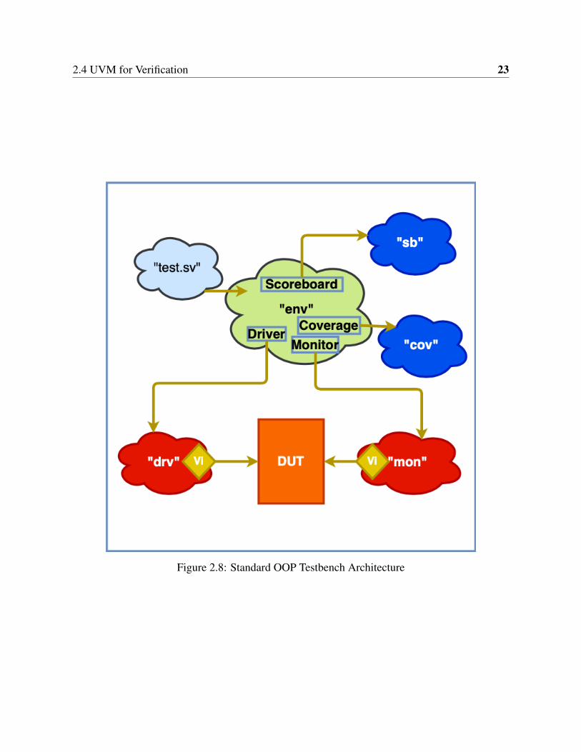
testbench with a constrained random stimulus [10]. Figure 2.8 shows a standard OOP testbench
architecture. It comprises of various components like program block, clocking block, interface,
packet, driver, environment, monitor, scoreboard, coverage and a top-level module that has the
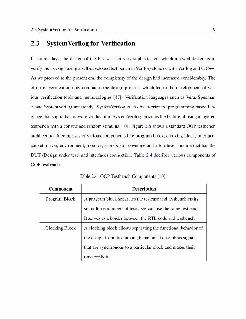
DUT (Design under test) and interfaces connection. Table 2.4 decribes various components of
OOP testbench.
Table 2.4: OOP Testbench Components [10]
Component Description
Program Block A program block separates the testcase and testbench entity,
so multiple numbers of testcases can use the same testbench.
It serves as a border between the RTL code and testbench.
Clocking Block A clocking block allows separating the functional behavior of
the design from its clocking behavior. It assembles signals
that are synchronous to a particular clock and makes their
time explicit.

2.3 SystemVerilog for Verification 20
Table 2.4: OOP Testbench Components [10]
Component Description
Interface In the purest form, an interface is simply a bundle of wire. It
is just like another module which can be instantiated and can
also instantiate other interfaces.
Driver The Drive is a design’s active entity. The driver component
has the logic that drives to DUT and sends data received from
the sequencer to the DUT. It continuously sends data to the
DUT and only stops when the sequencer stops sending data.
Monitor The Monitor stores, collects and monitors the transaction sent
from the DUT and the model. It also forwards the collected
transactions to the coverage checker.
Environment Agent, monitor, scoreboard, and coverage checkers are the
components of the environment, and the environment also
connects these components.
Scoreboard A scoreboard is used to check if the design is working as
expected. It compares the DUT output with the reference
model output.

2.3 SystemVerilog for Verification 21
Table 2.4: OOP Testbench Components [10]
Component Description
Coverage The percentage of the verification objectives met by design is
called coverage. Coverage metric is an important step to
evaluate the design. It also improves the quality of the
testbench. Coverage is classified into two types:
1. Code Coverage - Code coverage critiques on how good
the code is covered during the simulation. Code
coverage is an auxiliary add-on technology to the
language of Verilog. It is generated automatically by the
simulators.
2. Functional Coverage - The functional coverage is the
heart and soul of the RTL. It is user-defined and projects
how well the features have been applied to the design. It
checks the functionality of the design, covers corner
cases, and catches a significant number of design bugs.

2.4 UVM for Verification 22
Table 2.4: OOP Testbench Components [10]
Component Description
Assertions Assertion describes the function of the design. Assertions can
be used to provide functional coverage and to flag the input
stimulus. If the assertion has described property that
mismatches the specification, the assertion fails and gives an
error. There are two types of assertions:
1. Immediate Assertion - Immediate Assertions are
expression-based and execute as a statement in
procedural blocks. There are used only in dynamic
simulation.
2. Concurrent Assertion - Concurrent Assertions are clock
based and execute concurrently like other blocks. There
are used in both static and dynamic simulation.
2.4 UVM for Verification
The inability of SystemVerilog to support metaprogramming, reflection facilities, and unlimited
macro capabilities started the development and rapid adoption of UVM (Universal Verification
Methodology) [48]. UVM is a well-established verification approach based on SystemVerilog
for IP and SoC [49]. Accellera released UVM version 1.0 in February 2011. With the use of Sys-
temVerilog for creating components and transaction-level model to interconnect the component,
2.4 UVM for Verification 23
Figure 2.8: Standard OOP Testbench Architecture
2.4 UVM for Verification 24
UVM proves to be a standardized method for SoC verification. The UVM methodology also
enables easy use, and reuse, of Transaction Level Modeling (TLM) interfaces and components.
It also offers to improve verification efficiency, data portability, and interoperability between tool
and Verification IP [48, 50, 51].

Chapter 3
Architecture Overview
This chapter describes the design architecture of the DFI-AXI DDR4 Memory PHY Bridge.
Figure 3.1 shows the system-level architecture of the memory sub-system.
Figure 3.1: System-level Architecture of Memory Sub-system

3.1 SoC (DUT) Memory Controller 26
3.1 SoC (DUT) Memory Controller
The SoC Design under Test (DUT) includes a memory controller (MC) which provides a wide
range of address and data to the bridge module. It is responsible for sending the commands
signals, read signals, write signals, and other DFI interaction signals. It sends transfers signals
and requests to the DFI-AXI DDR4 Memory PHY Bridge module via the DFI. The next Section
3.2 provides a detailed explanation of signals from the MC.
3.2 DFI
The DFI interface is a standard interface protocol. It defines signals and timing parameters
required to transfer data and information to/from the DRAM and between the memory controller
and PHY. Several electronic devices like smartphone, computers, network system use DFI. Both
designs for MC and PHY separately done by different companies; this causes the necessity for
DFI interface. DFI grants two different companies IP designs to interoperate with each other
[52].
The following are notable features of the DFI protocol:
• Supports low power mode
– Here the PHY may enter to an MC initiated low power state if PHY predicts that DFI
will be in an idle state for an extended period.
• Increases the sharpness of signal placement
– DFI write training and read training operations boost the accuracy of signal placement
at a higher speed in the DDR system.
• MC to PHY frequency ratios

3.2 DFI 27
– DFI allows changing the clock frequency of the MC and PHY without re-setting the
entire system.
– It supports 1:1, 1:2, and 1:4 clock frequency ratio.
• Reduces power consumption and noise
– Data Bus Inversion reduces the number of transitions, which reduces power con-
sumption and noise.
3.2.1 Interface Group
The DFI specification is organized into the following interface groups, which consists of multiple
signals and their parameters [5]. Figure 3.2shows the block diagram of Interface Signals.
3.2.1.1 Command Interface
The command interface manages signals needed to drive the address and command signals to the
DRAM. These signals have to maintain their timing relationship to the DRAM device through the
DFI. The command interface is made up of Command Address (CA) bus. The CA bus contains
address, command signals and other information like bank/row. CA signals include dfi_act_n,
dfi_address, dfi_bank, dfi_we_n, dfi_ras_n, dfi_cas_n, dfi_bg, and these commands are listed
in Table 3.1 and Table 3.2 defines its timing parameters. The encoded read or write command
information is sent through the CA bus [5].

3.2 DFI 28
Figure 3.2: Block diagram of DDR PHY Interface signals [5]
3.2 DFI 29
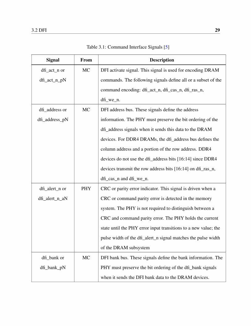
Table 3.1: Command Interface Signals [5]
Signal From Description
dfi_act_n or
dfi_act_n_pN
MC DFI activate signal. This signal is used for encoding DRAM
commands. The following signals define all or a subset of the
command encoding: dfi_act_n, dfi_cas_n, dfi_ras_n,
dfi_we_n.
dfi_address or
dfi_address_pN
MC DFI address bus. These signals define the address
information. The PHY must preserve the bit ordering of the
dfi_address signals when it sends this data to the DRAM
devices. For DDR4 DRAMs, the dfi_address bus defines the
column address and a portion of the row address. DDR4
devices do not use the dfi_address bits [16:14] since DDR4
devices transmit the row address bits [16:14] on dfi_ras_n,
dfi_cas_n and dfi_we_n.
dfi_alert_n or
dfi_alert_n_aN
PHY CRC or parity error indicator. This signal is driven when a
CRC or command parity error is detected in the memory
system. The PHY is not required to distinguish between a
CRC and command parity error. The PHY holds the current
state until the PHY error input transitions to a new value; the
pulse width of the dfi_alert_n signal matches the pulse width
of the DRAM subsystem
dfi_bank or
dfi_bank_pN
MC DFI bank bus. These signals define the bank information. The
PHY must preserve the bit ordering of the dfi_bank signals
when it sends the DFI bank data to the DRAM devices.

3.2 DFI 30
Table 3.1: Command Interface Signals [5]
Signal From Description
dfi_bg or
dfi_bg_pN
MC DFI bank group. This signal defines the bank group of a
command. The PHY must preserve the bit ordering of the
dfi_bg signals when it sends the DFI bank group data to the
DRAM devices.
dfi_cas_n or
dfi_cas_n_pN
MC DFI column address strobe. This signal is used for encoding
DRAM commands. The following signals define all or a
subset of the command encoding: dfi_act_n, dfi_cas_n,
dfi_ras_n, dfi_we_n.
dfi_cid or
dfi_cid_pN
MC DFI chip ID. This signal defines the chip ID. This signal is
required for 3D stacked solutions.
dfi_cke or
dfi_cke_pN
MC DFI clock enable. This signal defines the clock enable. The
MC must drive CKE signals in all phases. The PHY must be
able to accept a command on any and all phases for DFI
frequency ratio compliance.
dfi_cs or
dfi_cs_pN
MC DFI chip select. This signal defines the chip select. The
polarity of this signal is defined by the polarity of the
corresponding memory signal. For 3DS operation, also refer
to the dfi_cid signal.

3.2 DFI 31
Table 3.1: Command Interface Signals [5]
Signal From Description
dfi_dram_clk
_disable or
dfi_dram_clk
_disable_pN
MC DRAM clock disable. When active, this indicates to the PHY
that the clocks to the DRAM devices must be disabled such
that the clock signals hold a constant value. When the
dfi_dram_clk_disable signal is inactive, the DRAMs should
be clocked normally.
dfi_odt or
dfi_odt_pN
MC DFI on-die termination control bus. These signals define the
ODT. The MC must drive ODT signals in all phases. The
PHY must be able to accept a command on any and all phases
for DFI frequency ratio compliance.
dfi_parity_in or
dfi_parity_in_pN
MC Parity value. This signal has a one-to-one correspondence
with each DFI command and is valid for 1 cycle. This value
applies to the dfi_address, dfi_bank, dfi_bg, dfi_act_n,
dfi_cas_n, dfi_cid, dfi_ras_n and dfi_we_n signals. This signal
is relevant for only systems that support command parity.
’b0 = An even number of the parity value signals are
electrically high
’b1 = An odd number of the parity value signals are
electrically high
dfi_ras_n or
dfi_ras_n_pN
MC DFI row address strobe. This signal is used for encoding
DRAM commands. The following signals define all or a
subset of the command encoding: dfi_act_n, dfi_cas_n,
dfi_ras_n, dfi_we_n.

3.2 DFI 32
Table 3.1: Command Interface Signals [5]
Signal From Description
dfi_reset_n or
dfi_reset_n_pN
MC DFI reset bus. These signals define the RESET. The PHY
must preserve the bit ordering of the dfi_reset_n signals when
it sends the DFI chip ID data to the DRAM devices.
dfi_we_n or
dfi_we_n_pN
MC DFI write enable signal. This signal is used for encoding
DRAM commands. The following signals define all or a
subset of the command encoding: dfi_act_n, dfi_cas_n,
dfi_ras_n, dfi_we_n.
3.2.1.2 Write Data Interface
The write data interface is used to send write data across DFI that is it transfers signals from
the MC to the PHY [5]. The write data interface signals include dfi_wrdata_cs, dfi_wrdata_en,
dfi_wrdata, dfi_wrdata_mask, and these commands are listed in Table 3.4 and Table 3.5 lists its
parameters.
3.2.1.3 Read Data Interface
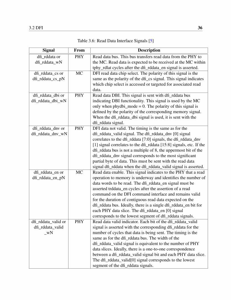
The read data interface is used to send read data across DFI that is it transfers signals from the
MC to the PHY [5]. The read data interface signals includes dfi_rddata_wN, dfi_rddata_en_pN,
dfi_rddata_cs_pN, dfi_rddata_dbi_wN, dfi_rddata_dnv_wN, dfi_rddata_valid_wN, and these
commands are listed in Table 3.6 and Table 3.7 lists its parameters.

3.2 DFI 33
Table 3.2: Command Interface Timing Parameters [5]
Parameter Definedby
Description
t_cmd_lat MC Specifies the number of DFI clocks after the dfi_cs signal isasserted until the associated CA signals are driven.
t_ctrl_delay PHY Specifies the number of DFI clock cycles from the time thatany command signal changes and when the change reachesthe DRAM interface. If the DFI clock and the DRAM clockare not phasealigned, this timing parameter should be roundedup to the next integer value.
t_dram_clk_disable PHY Specifies the number of DFI clock cycles from the assertion ofthe first phase of the dfi_dram_clk_disable_pN signal on theDFI until the clock to the DRAMs at the PHY-DRAMboundary maintains a low value.NOTE: This parameter may be specified as a fixed value, or asa constant based on other fixed values in the system.
t_dram_clk_enable PHY Specifies the number of DFI clock cycles from the deassertionof the first phase of the dfi_dram_clk_disable_pN signal onthe DFI until the first valid rising edge of the clock to theDRAMs at the PHY-DRAM boundary. NOTE: This parametermay be specified as a fixed value, or as a constant based onother fixed values in the system.
t_parin_lat MC Specifies the number of DFI PHY clocks between when theDFI command is asserted and when the associateddfi_parity_in signal is driven.
t_phy_paritylat PHY Specifies the maximum number of DFI clock cycles betweenwhen the dfi_parity_in signal is driven and when theassociated dfi_alert_n signal is returned.

3.2 DFI 34
Table 3.4: Write Data Interface Signals [5]
Signal From Descriptiondfi_wrdata or
dfi_wrdata_pNMC Write data. These signals transfer write data from the MC to
the PHY tphy_wrdata cycles after the dfi_wrdata_en signal isasserted and continues transferring data for the number ofcycles that the dfi_wrdata_en signal is asserted.
dfi_wrdata_csor
dfi_wrdata_cs_pN
MC DFI write data chip select. The polarity of this signal is thesame as the polarity of the dfi_cs signal. This signal indicatesthe chip select that is accessed or targeted for associated writedata.
dfi_wrdata_enor
dfi_wrdata_en_pN
MC Write data and data mask enable. This signal indicates to thePHY that valid dfi_wrdata will be transmitted in tphy_wrdatacycles. Both tphy_wrlat and tphy_wrdata may be defined aszero. Ideally, there is a one-to-one correspondence betweendfi_wrdata_en bits and PHY data slices. The dfi_wrdata_en[0] signal corresponds to the lowest segment of dfi_wrdatasignals.
dfi_wrdata_maskor
dfi_wrdata_mask_pN
MC Write data byte mask. This bus is used for transferring eitherthe write data mask or the write DBI information, dependingon system/DRAM settings. It uses the same timing as thedfi_wrdata signal. The polarity of this signal is defined by thepolarity of the corresponding memory signal.dfi_wrdata_mask [0] = Masking or DBI for the dfi_wrdata[7:0] signalsdfi_wrdata_mask [1] = Masking or DBI for the dfi_wrdata[15:8] signals, etc.If the dfi_wrdata bus is not a multiple of 8, the uppermost bitof the dfi_wrdata_mask signal corresponds to the mostsignificant partial byte of data.

3.2 DFI 35
Table 3.5: Write Data Interface Timing Parameters [5]
Parameter Definedby
Description
t_phy_wrcsgap PHY This parameter specifies the minimum number of additionalDFI PHY clocks (or DFI PHY clock) cycles that are requiredbetween commands when changing the target physical rankthat is driven on the dfi_wrdata_cs signal. This parametermust be supported in the MC transaction-to-transactiontiming. The minimum assertion duration of dfi_wrdata_cs isdetermined by tphy_wrcsgap + dfirw_length.
t_phy_wrcslat PHY This parameter specifies the number of DFI PHY clock cyclesfrom the time that a write command is sent on the DFIcommand interface and when the associated dfi_wrdata_cssignal is asserted.
t_phy_wrdata PHY This parameter specifies the number of DFI PHY clock cyclesfrom the time that the dfi_wrdata_en signal is asserted andwhen the associated write data is driven on the dfi_wrdatasignal. The parameter adjusts the relative time between enableand data transfer with no effect on performance. DFI 1.0 andDFI 2.0 MCs support a tphy_wrdata value of only 1. The MCshould support a range of tphy_wrdata values. A PHY isdesigned to operate at a single tphy_wrdata value.
t_phy_wrlat PHY This parameter specifies the number of DFI PHY clock cyclesfrom the time that a write command is sent on the DFIcommand interface and when the dfi_wrdata_en signal isasserted.
t_wrdata_delay System This parameter specifies the number of DFI clocks from thetime that the dfi_wrdata_en signal is asserted and when thecorresponding write data transfer completes on the DRAMbus.
3.2 DFI 36
Table 3.6: Read Data Interface Signals [5]
Signal From Descriptiondfi_rddata or
dfi_rddata_wNPHY Read data bus. This bus transfers read data from the PHY to
the MC. Read data is expected to be received at the MC withintphy_rdlat cycles after the dfi_rddata_en signal is asserted.
dfi_rddata_cs ordfi_rddata_cs_pN
MC DFI read data chip select. The polarity of this signal is thesame as the polarity of the dfi_cs signal. This signal indicateswhich chip select is accessed or targeted for associated readdata.
dfi_rddata_dbi ordfi_rddata_dbi_wN
PHY Read data DBI. This signal is sent with dfi_rddata busindicating DBI functionality. This signal is used by the MConly when phydbi_mode = 0. The polarity of this signal isdefined by the polarity of the corresponding memory signal.When the dfi_rddata_dbi signal is used, it is sent with thedfi_rddata signal.
dfi_rddata_dnv ordfi_rddata_dnv_wN
PHY DFI data not valid. The timing is the same as for thedfi_rddata_valid signal. The dfi_rddata_dnv [0] signalcorrelates to the dfi_rddata [7:0] signals, the dfi_rddata_dnv[1] signal correlates to the dfi_rddata [15:8] signals, etc. If thedfi_rddata bus is not a multiple of 8, the uppermost bit of thedfi_rddata_dnv signal corresponds to the most significantpartial byte of data. This must be sent with the read datasignal dfi_rddata when the dfi_rddata_valid signal is asserted.
dfi_rddata_en ordfi_rddata_en_pN
MC Read data enable. This signal indicates to the PHY that a readoperation to memory is underway and identifies the number ofdata words to be read. The dfi_rddata_en signal must beasserted trddata_en cycles after the assertion of a readcommand on the DFI command interface and remains validfor the duration of contiguous read data expected on thedfi_rddata bus. Ideally, there is a single dfi_rddata_en bit foreach PHY data slice. The dfi_rddata_en [0] signalcorresponds to the lowest segment of dfi_rddata signals.
dfi_rddata_valid ordfi_rddata_valid
_wN
PHY Read data valid indicator. Each bit of the dfi_rddata_validsignal is asserted with the corresponding dfi_rddata for thenumber of cycles that data is being sent. The timing is thesame as for the dfi_rddata bus. The width of thedfi_rddata_valid signal is equivalent to the number of PHYdata slices. Ideally, there is a one-to-one correspondencebetween a dfi_rddata_valid signal bit and each PHY data slice.The dfi_rddata_valid[0] signal corresponds to the lowestsegment of the dfi_rddata signals.

3.2 DFI 37
Table 3.7: Read Data Interface Timing Parameters [5]
Parameter Definedby
Description
t_phy_rdcsgap PHY Specifies the minimum number of additional DFI PHY clocksrequired between commands when changing the targetphysical rank driven on the dfi_rddata_cs signal. Thisparameter needs to be supported in the MCtransaction-to-transaction timing. The minimum assertionduration of dfi_rddata_cs is determined by tphy_rdcsgap +dfirw_length
t_phy_rdcslat PHY Specifies the number of DFI PHY clocks between when a readcommand is sent on the DFI command interface and when theassociated dfi_rddata_cs signal is asserted.
t_phy_rdlat PHY Specifies the maximum number of DFI PHY clock cyclesallowed from the assertion of the dfi_rddata_en signal to theassertion of each of the corresponding bits of thedfi_rddata_valid signal.
t_rddata_en System Specifies the number of DFI PHY clock cycles from theassertion of a read command on the DFI to the assertion of thedfi_rddata_en signal.

3.2 DFI 38
3.2.1.4 Update Interface
The update interface expedites commands transmitted through the DFI that require interference
or delay of signals [5]. The update interface signals are listed in Table 3.8and Table 3.9 lists its
parameters.
Table 3.8: Update Interface Signals [5]
Signal From Description
dfi_ctrlupd_ack PHY MC-initiated update acknowledge. The dfi_ctrlupd_ack signal
is asserted to acknowledge an MC-initiated update request.
The PHY is not required to acknowledge this request. While
this signal is asserted, the DFI bus must remain in the idle
state except for transactions specifically associated with the
update process. If the PHY acknowledges the request, the
dfi_ctrlupd_ack signal must be asserted before tctrlupd_min
occurs and the dfi_ctrlupd_req signal de-asserts. If the PHY
ignores the request, the dfi_ctrlupd_ack signal must remain
de-asserted until the dfi_ctrlupd_req signal is de-asserted. The
dfi_ctrlupd_req signal is guaranteed to be asserted for at least
tctrlupd_min cycles. The dfi_ctrlupd_ack signal cannot be
asserted after tctrlupd_min, occurs, even if dfi_ctrlupd_req is
still asserted.

3.2 DFI 39
Table 3.8: Update Interface Signals [5]
Signal From Description
dfi_ctrlupd_req MC MC-initiated update request. The dfi_ctrlupd_req signal is
used with an MC-initiated update to indicate that the DFI will
be in the idle state for some time, in which case the PHY may
perform an update. The dfi_ctrlupd_req signal must be
asserted for a minimum of tctrlupd_min cycles and a
maximum of tctrlupd_max cycles. A dfi_ctrlupd_req signal
assertion is an invitation for the PHY to update and does not
require a response. The behavior of the dfi_ctrlupd_req signal
is dependent on the dfi_ctrlupd_ack signal:
If the update is acknowledged by the PHY, the dfi_ctrlupd_req
signal remains asserted as long as the dfi_ctrlupd_ack signal is
asserted, but dfi_ctrlupd_ack must de-assert before
tctrlupd_max expires. While dfi_ctrlupd_req is asserted, the
DFI bus remains in the idle state except for transactions
specifically associated with the update process.
If the update is not acknowledged, the dfi_ctrlupd_req signal
may de-assert at any time after tctrlupd_min occurs and
before tctrlupd_max expires.
The MC may de-assert the dfi_ctrlupd_req signal to
disconnect the handshake through the disconnect protocol.

3.2 DFI 40
Table 3.8: Update Interface Signals [5]
Signal From Description
dfi_phyupd_ack MC PHY-initiated update acknowledge. The dfi_phyupd_ack
signal is used for a PHY-initiated update to indicate that the
DFI is idle and remains in the idle state until the
dfi_phyupd_req signal de-asserts. In most cases, the MC must
assert the dfi_phyupd_ack signal within tphyupd_resp cycles
of the dfi_phyupd_req signal; exceptions are granted when the
dfi_phymstr_req signal is also asserted. When the
dfi_phyupd_ack signal is asserted, it should remain asserted as
long as the dfi_phyupd_req signal remains asserted. The
dfi_phyupd_ack signal must de-assert upon the detection of
dfi_phyupd_req signal de-assertion. The dfi_phyupd_req
cannot be re-asserted prior to the de-assertion of
dfi_phyupd_ack for the previous transaction. The MC may
de-assert the dfi_phyupd_ack signal to disconnect the
handshake through the disconnect protocol.

3.2 DFI 41
Table 3.8: Update Interface Signals [5]
Signal From Description
dfi_phyupd_req PHY PHY-initiated update request. The dfi_phyupd_req signal is
used for a PHY-initiated update to indicate that the PHY
requires the DFI bus to be placed in an idle state and not send
control, read or write commands or data for a specified period
of time. The maximum time required is specified by the
tphyupd_typeX parameter associated with the
dfi_phyupd_type signal. Once asserted, the dfi_phyupd_req
signal must generally remain asserted until the request is
acknowledged by the assertion of the dfi_phyupd_ack signal
and the PHY’s internal update procedure has been completed.
Exceptions are granted if the dfi_ctrlupd_req,
dfi_phymstr_req or dfi_init_start signals are also asserted

3.2 DFI 42
Table 3.9: Update Interface Timing Parameters [5]
Parameter Definedby
Description
t_ctrlupd_interva MC Specifies the maximum number of DFI clock cycles that theMC may wait between assertions of the dfi_ctrlupd_req signal.
t_ctrlupd_max MC Specifies the maximum number of DFI clock cycles that thedfi_ctrlupd_req signal can assert.
t_ctrlupd_min MC Specifies the maximum number of DFI clock cycles after theassertion of the dfi_phyupd_req signal to the assertion of thedfi_phyupd_ack signal. Exceptions are granted ifdfi_init_start, dfi_ctrlupd_req, or dfi_phymstr_req are activealong with dfi_phyupd_req.
t_phyupd_type0 PHY Specifies the maximum number of DFI clock cycles that thedfi_phyupd_req signal may remain asserted after the assertionof the dfi_phyupd_ack signal for dfi_phyupd_type = 0x0. Thedfi_phyupd_req signal may de-assert at any cycle after theassertion of the dfi_phyupd_ack signal.
t_phyupd_type1 PHY Specifies the maximum number of DFI clock cycles that thedfi_phyupd_req signal may remain asserted after the assertionof the dfi_phyupd_ack signal for dfi_phyupd_type = 0x1. Thedfi_phyupd_req signal may de-assert at any cycle after theassertion of the dfi_phyupd_ack signal.
t_phyupd_type2 PHY Specifies the maximum number of DFI clock cycles that thedfi_phyupd_req signal may remain asserted after the assertionof the dfi_phyupd_ack signal for dfi_phyupd_type = 0x2. Thedfi_phyupd_req signal may de-assert at any cycle after theassertion of the dfi_phyupd_ack signal.
t_phyupd_type3 PHY Specifies the maximum number of DFI clock cycles that thedfi_phyupd_req signal may remain asserted after the assertionof the dfi_phyupd_ack signal for dfi_phyupd_type = 0x3. Thedfi_phyupd_req signal may de-assert at any cycle after theassertion of the dfi_phyupd_ack signal.
3.2 DFI 43
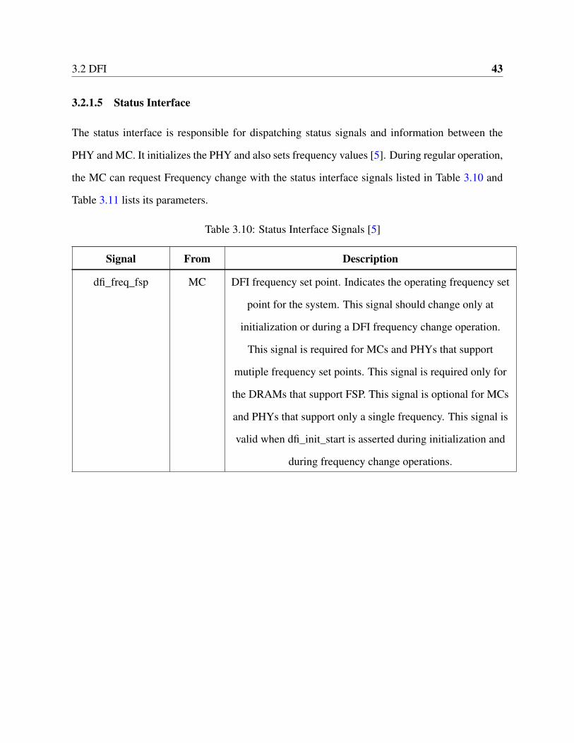
3.2.1.5 Status Interface
The status interface is responsible for dispatching status signals and information between the
PHY and MC. It initializes the PHY and also sets frequency values [5]. During regular operation,
the MC can request Frequency change with the status interface signals listed in Table 3.10 and
Table 3.11 lists its parameters.
Table 3.10: Status Interface Signals [5]
Signal From Description
dfi_freq_fsp MC DFI frequency set point. Indicates the operating frequency set
point for the system. This signal should change only at
initialization or during a DFI frequency change operation.
This signal is required for MCs and PHYs that support
mutiple frequency set points. This signal is required only for
the DRAMs that support FSP. This signal is optional for MCs
and PHYs that support only a single frequency. This signal is
valid when dfi_init_start is asserted during initialization and
during frequency change operations.

3.2 DFI 44
Table 3.10: Status Interface Signals [5]
Signal From Description
dfi_freq_ratio MC DFI frequency ratio indicator. This signal defines the
frequency ratio for the system. This signal is required for
MCs and PHYs that support multiple frequency ratios and the
DFI frequency ratio protocol. This signal is optional for MCs
and PHYs that support only a single frequency ratio or do not
support the DFI frequency ratio protocol. This signal is only
valid when the dfi_init_start signal is asserted during
initialization and frequency changes.
’b00 = 1:1 MC:PHY frequency ratio (matched frequency)
’b01 = 1:2 MC:PHY frequency ratio
’b10 = 1:4 MC:PHY frequency ratio
’b11 = Reserved For memories that support a frequency ratio
only for data, the signal defines the frequency ratio for the
data interface.
dfi_frequency MC DFI frequency. This signal indicates the operating frequency
for the system. This signal should change only at
initialization, during a DFI frequency change operation, or
other times that the system defines. The number of supported
frequencies and the mapping of signal values to clock
frequencies are defined by the PHY, system, or both. This
signal should be constant during normal operation.

3.2 DFI 45
Table 3.10: Status Interface Signals [5]
Signal From Description
dfi_init_complete PHY PHY initialization complete. The dfi_init_complete signal
indicates that the PHY is able to respond to any proper
stimulus on the DFI. All DFI signals that communicate
commands or status must be held at their default values until
the dfi_init_complete signal asserts. During a PHY
reinitialization request (such as a frequency change), this
signal is de-asserted. For a frequency change request, the
de-assertion of the dfi_init_complete signal acknowledges the
frequency change protocol. Once de-asserted, the signal
should only be re-asserted within tinit_complete cycles after
the dfi_init_start signal has de-asserted, and once the PHY has
completed reinitialization.

3.2 DFI 46
Table 3.11: Status Interface Timing Parameters [5]
Parameter Definedby
Description
t_init_complete PHY During a frequency change operation, specifies the maximumnumber of DFI clock cycles after the deassertion of thedfi_init_start signal to the reassertion of the dfi_init_completesignal.
t_init_complete_min PHY Minimum number of DFI clocks before dfi_init_complete canbe driven after a previous command.
t_init_start MC During a frequency change operation, this parameter specifiesthe number of DFI clock cycles from the assertion of thedfi_init_start signal on the DFI until the PHY must respond byde-asserting the dfi_init_complete signal. If thedfi_init_complete signal is not de-asserted within this timeperiod, the PHY indicates that it can not support the frequencychange at this time. In this case, the MC must abort therequest and release the dfi_init_start signal. After tinit_startexpires, the PHY must not de-assert the dfi_init_completesignal. The MC
t_init_start_min PHY Minimum number of DFI clocks before dfi_init_start can bedriven after a previous command.

3.2 DFI 47
3.2.1.6 Low Power Control Interface
The lower power control interface allows the PHY to enter power-saving mode [5].Table 3.12
shows the list of the Error Interface signals and Table 3.13 lists its parameters.
Table 3.12: Low Power Control Interface Signals [5]
Signal From Description
dfi_lp_ctrl_ack PHY Control low power acknowledge. The dfi_lp_ctrl_ack signal is
asserted to acknowledge the MC control low power
opportunity request. The PHY is not required to acknowledge
this request. If the PHY acknowledges the request, the
dfi_lp_ctrl_ack signal must be asserted within tlp_resp cycles
after the dfi_lp_ctrl_req signal assertion. Once asserted, this
signal remains asserted until the dfi_lp_ctrl_req signal
de-asserts. The signal de-asserts within tlp_ctrl_wakeup
cycles after the dfi_lp_ctrl_req signal de-asserts, indicating
that the PHY is able to resume normal operation. If the PHY
ignores the request, the dfi_lp_ctrl_ack signal must remain
de-asserted for the remainder of the low power mode
opportunity. The dfi_lp_ctrl_req signal is asserted for at least
tlp_resp cycles.

3.2 DFI 48
Table 3.12: Low Power Control Interface Signals [5]
Signal From Description
dfi_lp_ctrl_req MC Control low power opportunity request. The dfi_lp_ctrl_req
signal is used by the MC to inform the PHY of an opportunity
to switch to a low power mode. When asserted, the MC
indicates that no more commands will be sent on the
command interface. The MC must assert a constant value on
the dfi_lp_ctrl_wakeup signal while this signal is asserted
before the request is acknowledged by the PHY through the
assertion of the dfi_lp_ctrl_ack signal or until tlp_resp cycles
have elapsed. The MC may increase the value of the
dfi_lp_ctrl_wakeup signal while the dfi_lp_ctrl_req signal is
asserted. Following the de-assertion of the dfi_lp_ctrl_req
signal, the PHY has tlp_ctrl_wakeup cycles to resume normal
operation and de-assert the dfi_lp_ctrl_ack signal.

3.2 DFI 49
Table 3.12: Low Power Control Interface Signals [5]
Signal From Description
dfi_lp_ctrl_wakeup MC Control low power wakeup time. The dfi_lp_ctrl_wakeup
signal indicates which one of the 16 wakeup times the MC is
requesting for the PHY. The signal is only valid when the
dfi_lp_ctrl_req signal is asserted. The dfi_lp_ctrl_wakeup
signal must remain constant until the dfi_lp_ctrl_ack signal is
asserted. Once the request has been acknowledged, the MC
may increase the dfi_lp_ctrl_wakeup signal, permitting the
PHY to enter a lower power state. The PHY is not required to
change power states in response to the wakeup time change.
The MC may not decrease this value once the request has
been acknowledged. The value of the dfi_lp_ctrl_wakeup
signal at the time that the dfi_lp_ctrl_req signal is deasserted
sets the tlp_ctrl_wakeup time.
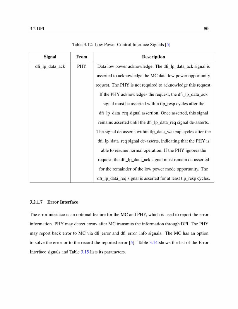
3.2 DFI 50
Table 3.12: Low Power Control Interface Signals [5]
Signal From Description
dfi_lp_data_ack PHY Data low power acknowledge. The dfi_lp_data_ack signal is
asserted to acknowledge the MC data low power opportunity
request. The PHY is not required to acknowledge this request.
If the PHY acknowledges the request, the dfi_lp_data_ack
signal must be asserted within tlp_resp cycles after the
dfi_lp_data_req signal assertion. Once asserted, this signal
remains asserted until the dfi_lp_data_req signal de-asserts.
The signal de-asserts within tlp_data_wakeup cycles after the
dfi_lp_data_req signal de-asserts, indicating that the PHY is
able to resume normal operation. If the PHY ignores the
request, the dfi_lp_data_ack signal must remain de-asserted
for the remainder of the low power mode opportunity. The
dfi_lp_data_req signal is asserted for at least tlp_resp cycles.
3.2.1.7 Error Interface
The error interface is an optional feature for the MC and PHY, which is used to report the error
information. PHY may detect errors after MC transmits the information through DFI. The PHY
may report back error to MC via dfi_error and dfi_error_info signals. The MC has an option
to solve the error or to the record the reported error [5]. Table 3.14 shows the list of the Error
Interface signals and Table 3.15 lists its parameters.
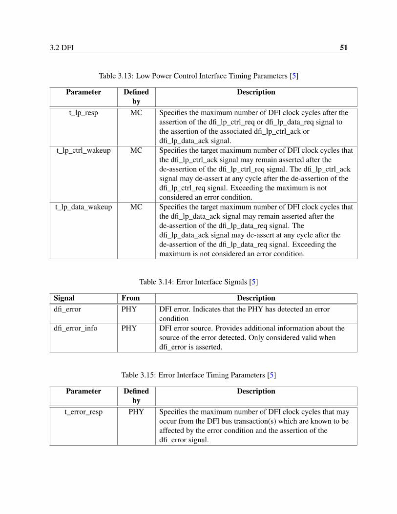
3.2 DFI 51
Table 3.13: Low Power Control Interface Timing Parameters [5]
Parameter Definedby
Description
t_lp_resp MC Specifies the maximum number of DFI clock cycles after theassertion of the dfi_lp_ctrl_req or dfi_lp_data_req signal tothe assertion of the associated dfi_lp_ctrl_ack ordfi_lp_data_ack signal.
t_lp_ctrl_wakeup MC Specifies the target maximum number of DFI clock cycles thatthe dfi_lp_ctrl_ack signal may remain asserted after thede-assertion of the dfi_lp_ctrl_req signal. The dfi_lp_ctrl_acksignal may de-assert at any cycle after the de-assertion of thedfi_lp_ctrl_req signal. Exceeding the maximum is notconsidered an error condition.
t_lp_data_wakeup MC Specifies the target maximum number of DFI clock cycles thatthe dfi_lp_data_ack signal may remain asserted after thede-assertion of the dfi_lp_data_req signal. Thedfi_lp_data_ack signal may de-assert at any cycle after thede-assertion of the dfi_lp_data_req signal. Exceeding themaximum is not considered an error condition.
Table 3.14: Error Interface Signals [5]
Signal From Descriptiondfi_error PHY DFI error. Indicates that the PHY has detected an error
conditiondfi_error_info PHY DFI error source. Provides additional information about the
source of the error detected. Only considered valid whendfi_error is asserted.
Table 3.15: Error Interface Timing Parameters [5]
Parameter Definedby
Description
t_error_resp PHY Specifies the maximum number of DFI clock cycles that mayoccur from the DFI bus transaction(s) which are known to beaffected by the error condition and the assertion of thedfi_error signal.

3.2 DFI 52
3.2.1.8 PHY Master Interface
The PHY Master Interface sets the DRAM in a defined state and provides resources to the PHY
to control DFI and DRAM buses [5]. The signals in the PHY Master Interface are listed in Table
3.16 and Table 3.17lists its parameters.
Table 3.16: PHY Master Interface Signals [5]
Signal From Description
dfi_phymstr_ack MC DFI PHY master acknowledge. When asserted, the MC places
the DRAM in a known state (IDLE, self-refresh, or
self-refresh power-down). When the dfi_phymstr_ack signal
is asserted, the PHY is the master of DRAM bus. If required
by the DRAM, the controller continues sending refresh
commands on the DFI bus.

3.2 DFI 53
Table 3.16: PHY Master Interface Signals [5]
Signal From Description
dfi_phymstr_cs_state PHY DFI PHY master CS state. This signal indicates the state of
the DRAM when the PHY becomes the master. Each memory
rank uses one bit.
’b0 = IDLE or self-refresh. The PHY specifies the required
state, using the dfi_phymstr_state_sel signal. For memories
that support self-refresh without being in the power-down
state, this state must be self-refresh without power-down.
’b1 = IDLE or self-refresh or self-refresh with powerdown.
The PHY does not specify the state; the MC can optionally
choose any supported state.
The MC closes all the pages prior to acknowledging the
request from the PHY. This signal is valid only when the
dfi_phymstr_req signal is asserted by the PHY and should
remain constant while the dfi_phymstr_req signal is asserted.
The dfi_phymstr_cs_state bit values are not relevant for chip
selects with syscs_state set to ’b0 (inactive chip selects). The
MC can leave the chip selects with syscs_state set to ’b0 in
their current, inactive state, regardless of the corresponding
dfi_phymstr_cs_state bit value. The PHY must not require
these chip selects to be in IDLE or self-refresh states. The
system must maintain a consistent, stable view of syscs_state
after dfi_phymstr_req is asserted to ensure synchronization
between the MC and PHY.

3.2 DFI 54
Table 3.16: PHY Master Interface Signals [5]
Signal From Description
dfi_phymstr_req PHY DFI PHY master request. When asserted, the PHY requests
control of the DFI bus. The systems must maintain a
consistent, stable view of syscs_state after dfi_phymstr_req is
asserted for ensuring synchronization between the MC and
PHY.
dfi_phymstr_state
_sel
PHY DFI PHY master state select. Indication from the PHY to the
MC whether the requested memory state is IDLE or
selfrefresh. If the per-CS dfi_phymstr_cs_state = 1, this signal
does not apply for that chip select. The PHY does not place
any requirement on the low power state of the memory, the
state may be IDLE, self-refresh, or self-refresh with
powerdown.
If the per-CS dfi_phymstr_cs_state = 0, for that chip select:
’b0 = The MC must place the memory on the associated CS in
the IDLE state.
’b1 = The MC must place the memory on the associated CS in
the self-refresh state.
For memories that support self-refresh without being in the
power-down state, this state must be self-refresh without
power-down. This signal is valid only when the
dfi_phymstr_req signal is asserted by the PHY and should
remain constant while that signal is asserted.

3.2 DFI 55
Table 3.17: PHY Master Interface Timing Parameters [5]
Parameter Definedby
Description
t_phymstr_resp MC Specifies the maximum number of DFI clock cycles after thedfi_phymstr_req signal asserts to the assertion of thedfi_phymstr_ack signal. Exceptions are granted ifdfi_init_start, dfi_lp_ctrl_req or dfi_lp_data_req is activealong with dfi_phymstr_req.
t_phymstr_rfsh PHY Specifies the maximum number of DFI clock cycles that thePHY requires for generating a refresh command to the DRAMafter the PHY receives the refresh command from the MC.
t_phymstr_type0 PHY Specifies the maximum number of DFI clock cycles that thedfi_phymstr_req signal may remain asserted after theassertion of the dfi_phymstr_ack signal for dfi_phymstr_type= 0x0. The dfi_phymstr_req signal may de-assert at any cycleafter the assertion of the dfi_phymstr_ack signal.
t_phymstr_type1 PHY Specifies the maximum number of DFI clock cycles that thedfi_phymstr_req signal may remain asserted after theassertion of the dfi_phymstr_ack signal for dfi_phymstr_type= 0x1. The dfi_phymstr_req signal may de-assert at any cycleafter the assertion of the dfi_phymstr_ack signal.
t_phymstr_type2 PHY Specifies the maximum number of DFI clock cycles that thedfi_phymstr_req signal may remain asserted after theassertion of the dfi_phymstr_ack signal for dfi_phymstr_type= 0x2. The dfi_phymstr_req signal may de-assert at any cycleafter the assertion of the dfi_phymstr_ack signal.
t_phymstr_type3 PHY Specifies the maximum number of DFI clock cycles that thedfi_phymstr_req signal may remain asserted after theassertion of the dfi_phymstr_ack signal for dfi_phymstr_type= 0x3. The dfi_phymstr_req signal may de-assert at any cycleafter the assertion of the dfi_phymstr_ack signal.

3.2 DFI 56
Table 3.18: Disconnect Protocol [5]
Signal From Descriptiondfi_disconnect_error MC DFI disconnect error. Indicates if the current disconnect is an
error or a QOS (fully operational) request. If de-asserted, thedisconnect request requires that the PHY remain fullyoperational after the disconnect. If asserted, the PHY mightnot be fully operational after the disconnect
Table 3.19: Disconnect Protocol Timing Parameters [5]
Parameter Definedby
Description
t_ctrlupd_disconnect PHY Defines the maximum number of clocks that are requiredto disconnect the PHY during a controller updatesequence, from the de-assertion of dfi_ctrlupd_req to thede-assertion of dfi_ctrlupd_ack whendfi_disconnect_error = ’b0.
3.2.1.9 Disconnect Protocol
Table 3.18 shows the list of the Disconnect signal and Table 3.19 lists its parameters.
3.2.1.10 2N Mode Interface
Table 3.20 shows the list of the 2N mode Interface signals and Table 3.21 lists its parameters.
Table 3.20: 2N Mode Interface Signals [5]
Signal From Descriptiondfi_2n_mode MC DFI 2N Mode. When de-asserted, the MC and PHY operate
normally. When asserted, the MC and PHY operate in 2Nmode. For DDR4, the MC can change CA signals only everyother DFI PHY clock as defined by the synchronization pulsefrom the PHY. For DDR5, there is no timing restriction.

3.2 DFI 57
Table 3.21: 2N Mode Interface Timing Parameters [5]
Parameter Definedby
Description
t_2n_mode_delay PHY The delay from dfi_2n_mode assertion to the time that thePHY is ready to receive commands.
Table 3.22: MC to PHY Message Interface Signals [5]
Signal From Descriptiondfi_ctrlmsg MC DFI Controller Message Command. Valid only when the
dfi_ctrlmsg_req signal is asserted. Encodes messages from theMC to the PHY.
dfi_ctrlmsg_ack PHY DFI Controller Message Acknowledge. When asserted,indicates that the PHY received the MC message. If themessage is to be acknowledged, the dfi_ctrlmsg_ack signalmust assert by within tctrlmsg_resp clock cycles. Onceasserted, the dfi_ctrlmsg_ack signal must de-assert withintctrlmsg_max clock cycles.
dfi_ctrlmsg_data MC DFI Controller Message Data. Valid only when thedfi_ctrlmsg_req signal is asserted. Data associated with theinfo command from the MC to the PHY.
dfi_ctrlmsg_data PHY DFI Controller Message Request. When asserted, indicates avalid MC to PHY message. If acknowledged, the request mustremain asserted until the dfi_ctrlmsg_ack signal is deasserted.If not acknowledged within tctrlmsg_resp, the request shouldbe de-asserted.
3.2.1.11 MC to PHY Message Interface
Table 3.22 shows the list of the MC to PHY Message Interface signals and Table 3.23 lists its
parameters.
3.2.1.12 WCK Control Interface
Table 3.24 shows the list of the WCK Control Interface signals and Table 3.25 lists its parameters.

3.2 DFI 58
Table 3.23: MC to PHY Message Interface Timing Parameters [5]
Parameter Definedby
Description
t_ctrlmsg_max MC Specifies the maximum number of DFI clocks that thedfi_ctrlmsg_ack signal can remain asserted.
t_ctrlmsg_resp MC Specifies the maximum number of DFI clock cycles betweenthe assertion of the dfi_ctrlmsg_req signal to the assertion ofthe dfi_ctrlmsg_ack signal.
Table 3.24: WCK Control Interface Signals [5]
Signal From Descriptiondfi_wck_cs or
dfi_wck_cs_pNMC WCK chip select. This signal indicates which chip selects
currently have the WCK active. More than one chip select canbe active at a time. There is one bit per chip select. This signalis only valid when the dfi_wck_en signal is asserted.
dfi_wck_en ordfi_wck_en_pN
MC WCK clock enable. This signal defines when the WCK clockis driven or disabled (tri-state).’b0 = WCK disabled’b1 = WCK enabled
dfi_wck_toggle ordfi_wck_toggle_pN
MC WCK toggle. This is a 2-bit encoded value defining the stateof the WCK clock. This signal is only valid when thedfi_wck_en signal is asserted.’b00 = WCK static low’b01 = WCK static high’b10 = WCK toggle’b11 = WCK fast-toggle
Table 3.25: WCK Control Interface Timing Parameters [5]
Parameter Definedby
Description
t_wck_dis PHY Defines the number of clock cycles between the last command(LAST CMD) without a WCK synchronization required(assuming no command issued) or any command that disablesthe WCK to when the dfi_wck_en signal is disabled.
t_wck_en_fs PHY Defines the number of clocks between the CAS_WS_FScommand to when the dfi_wck_en signal is driven.
t_wck_en_rd PHY Defines the number of clocks between the CAS_WS_RDcommand to when the dfi_wck_en signal is driven.
3.3 DFI-AXI DDR4 Memory PHY Bridge 59
3.3 DFI-AXI DDR4 Memory PHY Bridge
The DFI-AXI DDR4 Memory PHY Bridge is compatible with all types of DDR memory sub-
systems. The main objective of the bridge is to process DFI commands and translate and forward
commands as an AXI master. In typical use, the DFI-AXI DDR4 Memory PHY Bridge would
communicate via AXI to a FPGA base memory controller such as the Xilinx DDR4 memory sub-
system for re-processing. The bridge also filters out extra non-essential commands, functional
modes, and interface groups which are not needed and cannot be forwarded. The DFI-AXI
DDR4 Memory PHY Bridge contains into four main blocks:
3.3.1 Command Transaction Unit
3.3.1.1 Initialization Unit
Initialization unit performs the starts-up and power-up the initialization before carrying out read
and write transactions. The MC asserts the dfi_init_start signal to begin the initialization pro-
cess and to indicate that valid values are on the DFI. The DFI-AXI DDR4 Memory PHY Bridge
module uses this asserted dfi_init_start signal to indicate that status signal is valid then asserts
the dfi_init_complete signal. The dfi_freq_ratio signal defines MC to PHY frequency ratio. In
our case the dfi_ freq_ratio signal supports the standard frequency ratios (1:1, 1:2 or 1:4). The
bridge module must wait for the dfi_init_start signal before asserting the dfi_init_complete sig-
nal. MC can hold the assert or de-assert the dfi_init_start after asserting both the dfi_init_start
and dfi_init_complete signal for a minimum of one clock. The dfi_init_start signal also defines
the dfi_frequency signal with the dfi_init_freq timing parameter. Upon completing of these com-
mands, the DFI-AXI DDR4 Memory PHY Bridge module is ready to start the regular operation.

3.3 DFI-AXI DDR4 Memory PHY Bridge 60
3.3.1.2 Control Unit
The controller unit in the DFI-AXI DDR4 Memory PHY Bridge module waits for completion
of initialization and then configures registers. The MC sends an address to the bridge mod-
ule through the dfi_address_pN_r. The bridge module receives two kinds of address on the
dfi_address_pN signal. The first is column address which is received on the rising edge of the
clock followed by the row address signal on the next rising edge of the clock. The control unit
is responsible for decoding the valid read and write address from the MC. The format of a valid
address is bank, bank group, row address, column address. Where row and column address
are each16 bit and bank and bank group are each 2 bits. The control unit fetches data from
dfi_address_pN, dfi_bank_pN, dfi_bg_pN, and forms a valid address for further transactions.
3.3.1.3 Decode Command Unit
The decode command unit in the DFI-AXI DDR4 Memory PHY Bridge module waits for
completion of initialization and then accepts other signals from the MC. This unit keeps
track of the dfi_cke_pN_rr, dfi_cke_pN_r, dfi_cs_n_pN_r, dfi_act_n_pN_r, dfi_ras_n_pN_r,
dfi_cas_n_pN_r, dfi_we_n_pN_r signals. The MC has fours phase dr4_cmd_p0, dr4_cmd_p1,
dr4_cmd_p2 and dr4_cmd_p3. The MC can operate with single or multiple command phase
depending on the frequency. This unit tracks the signals and projects the command based on the
signal. It also maintains counters for total number times a command was received. The com-
mands decoded are MRS, REF, SRE, SRX, PRE, RFU, ACT, NOP, DES, PDE, PDZX, ZQ. After
decoding the commands, this unit filters out decode commands and sends it to the SCE-MI.

3.3 DFI-AXI DDR4 Memory PHY Bridge 61
3.3.2 Write Transaction Unit
The DFI-AXI DDR4 Memory PHY Bridge write transaction unit is divided into parts. The first
part is the write FSM which decodes the write address and write data commands from the MC.
The second part of the write transaction unit is write channel. The write channel consists of the
asynchronous FIFO for crossing the two different clock domains.
3.3.2.1 Write FSM
The write finite state machine is liable for all the write transactions between the MC and the
AXI. It waits for the initialization of the MC and then accepts commands from the MC. Figure
3.3 shows the state diagram of write FSM. The write FSM has four states WR_IDLE, WR_EN,
WR_WAIT, and WR_DATA. Whenever the reset signal is low, the write FSM (WRSTATE)
switches to WR_IDLE state. This WR_IDLE state continuously checks for dfi_cs_n_p0_r,
dfi_cas_n_p0_r, dfi_we_n_p0_r signals to be low and dfi_act_n_p0_r, dfi_ras_n_p0_r signals
to be high. If the check of the signals matches, then the write FSM (WRSTATE) moves to the
WR_EN state. In the WR_EN state, the write FSM (WRSTATE) controls the write data queue
and carries out four things. It asserts the waddr_q_wr_en signal of the write address channel. It
checks if the waddr_q_full is low. If the waddr_q_full is low, it writes the valid address (AWAD-
DRESS) and SCE-MI message to the waddr_q_in_data. It looks for the dfi_t_phy_wrlat param-
eter if the parameter is zero the write FSM moves forward to the WR_DATA state. If not zero,
then the write FSM moves to the WAIT_WRDATA. The WAIT_WRDATA state consists of a de-
lay counter that decrements every clock cycle. The write FSM moves forward to the WR_DATA
state when the delay counter hits zero. The WR_DATA state checks if the wdata_q_full is low
of the write data channel. When MC requests a write command the write FSM stores the address
and data. Depending on the burst type of 4 or 8, the data will be packed in 2 or 4 beats respec-

3.3 DFI-AXI DDR4 Memory PHY Bridge 62
tively. If the wdata_q_full is low, it writes the valid data (WRDATA) and SCE-MI message to the
wdata_q_in_data. After, the completion of writing sequence to the write data channel the write
FSM moves back to the WR_IDLE state.
Figure 3.3: Write Finite State Machine
3.3.2.2 Write FIFO
Write FIFO block consists of three independent FIFOs used as queues: Write Address FIFO,
Write Data FIFO, and Write Response FIFO. The DFI clock (dfi_clock) is used to write into
these independent queues, and AXI clock (aclk) is used to read from these independent queues.

3.3 DFI-AXI DDR4 Memory PHY Bridge 63
Data-in from the source clock domain and data-out from destination clock domain using asyn-
chronous FIFO is most secured design technique for clock domain crossing. The Write Address
FIFO holds MessageIn from the SCE-MI and write address, the Write Data FIFO holds Mes-
sageIn from the SCE-MI and write data, the Write Response FIFO holds MessageOut and write
response.
3.3.3 Read Transaction Unit
The DFI-AXI DDR4 Memory PHY Bridge read transaction unit is divided into parts. The first
part is the read FSM which decodes the read address commands from the MC. The second part
of the read transaction unit is read channel. The read channel consists of the asynchronous FIFO
for crossing the two different clock domains.
3.3.3.1 Read FSM
The read finite state machine is responsible for all the read transactions between the MC and the
AXI. It waits for the initialization of the MC and then accepts commands from the MC. Figure
3.4 shows the state diagram of read FSM. The read FSM has four states RD_IDLE, RD_EN,
RD_WAIT, and RD_DATA. Whenever the reset signal is low, the read FSM (RDSTATE)
switches to RD_IDLE state. This RD_IDLE state continuously checks for dfi_cs_n_p0_r,
dfi_cas_n_p0_r signals to be low and dfi_act_n_p0_r , dfi_ras_n_p0_r, dfi_we_n_p0_r signals
to be high. If the check of the signals matches, then the write FSM (RDSTATE) moves to the
RD_EN state. In the RD_EN state, the read FSM (RDSTATE) controls the read channel and
carries out four things. It asserts the raddr_q_wr_en signal of the read address channel. It checks
if the raddr_q_full is low. If the raddr_q_full is low, it writes the valid address (AWADDRESS)
and SCE-MI message to the raddr_q_in_data. It looks for the dfi_t_phy_rdlat parameter if the
parameter is zero the write FSM moves forward to the WR_DATA state. If not zero, then the

3.3 DFI-AXI DDR4 Memory PHY Bridge 64
write FSM moves to the WAIT_RDDATA. The WAIT_RDDATA state consists of a delay counter
that decrements every clock cycle. The write FSM moves forward to the RD_DATA state when
the delay counter hits zero. The RD_DATA state checks if the rdata_q_empty is high of the read
data channel. If the rdata_q_empty is high, it writes the valid data from the rdata_q_out_data to
dfi_rddata_wN. After, the completion of writing sequence to the dfi_rddata_wN the read FSM
moves back to the RD_IDLE state.
Figure 3.4: Read Finite State Machine

3.3 DFI-AXI DDR4 Memory PHY Bridge 65
3.3.3.2 Read FIFO
Read FIFO block consists of two independent FIFOs used as queues: Read Address FIFO and
Read Response FIFO. The DFI clock (dfi_clock) is used to write into the Read Address queue,
and AXI clock (aclk) is used to read from these Read Address queue; data read from the AXI is
written into the Read Response queue using the AXI clock (aclk), and DFI clock (dfi_clock) is
used to read from the Read Response queue. Data-in from the source clock domain and data-out
from destination clock domain using asynchronous FIFO is most secured design technique for
clock domain crossing. The Read Address FIFO holds MessageIn from the SCE-MI and read
address, the Read Response FIFO holds MessageOut and read data.
3.3.4 Interactions Unit
3.3.4.1 DFI interactions FSM
DFI interactions FSM describes how the bridge module handles interactions between the Up-
date, Status, PHY Master, and Low Power Interfaces. Figure 3.5 shows the state diagram of
the DFI Interactions FSM. The Interaction FSM filters out PHY based commands or responses
and forwards it to the SCE-MI controller. The DFI Interactions (INTERACTIONSTATE) FSM
has ten states INTERACTION_IDLE, TPHYUPD, TPHYMSTR, PHYUPD_REQ, PHY_REQ,
UPD_REQ, PHYUPD_INITSTART_REQ, PHYMSTR_REQ, PHYMSTR_INITSTART_REQ,
PHYMSTR_LP_REQ. Whenever the reset signal is low, the INTERACTIONSTATE switches to
INTERACTION_IDLE. The interaction state will then monitor the signals, as shown in Table
3.26 and change its state accordingly.

3.3 DFI-AXI DDR4 Memory PHY Bridge 66
Figure 3.5: DFI Interactions State Machine

3.3 DFI-AXI DDR4 Memory PHY Bridge 67
Table 3.26: Truthtable of DFI Interaction Signals
dfi_
phyupd
_req_r
dfi
_phymstr
_req_r
dfi_
ctrlupd
_req_r
dfi_init
_start_r
dfi_lp_
ctrl_
req_r
dfi_lp_
data_
req_r
INTER-
ACTION
STATE
INTER-
ACTION
NEXT
STATE
1 0 0 0 x x TPHYUPD PHYUPD
_REQ
1 1 0 0 x x TPHYUPD PHY_REQ
1 0 1 0 x x TPHYUPD UPD_REQ
1 0 0 1 x x TPHYUPD PHYUPD
_INITSTART
_REQ
0 1 0 0 0 0 TPHYMSTR PHYMSTR
_REQ
0 1 0 1 0 0 TPHYMSTR PHYMSTR
_INITSTART
_REQ
0 1 0 0 1 1 TPHYMSTR PHYMSTR
_LP
_REQ
The MC has the following requirements from the PHY. In our case, the Bridge module will
support all the PHY responses [5].
• MC requirement to assert dfi_phyupd_ack in response to dfi_phyupd_req PHY require-

3.4 SCE-MI 68
ment to maintain dfi_phyupd_req until dfi_phyupd.
• MC requirement to assert dfi_phymstr_ack in response to dfi_phymstr_req.
• MC must never have both dfi_ctrlupd_req and dfi_init_start asserted.
• MC must never have both dfi_lp_ctrl_req, and dfi_init_start asserted.
• MC must never have both dfi_lp_data_req, and dfi_init_start asserted.
3.3.4.2 SCE-MI Controller
The Interaction FSM filters out PHY based commands, responses, and forwards it to the SCE-
MI controller. The SCE-MI controller interacts with the SCE-MI to gain information about the
parameters [15]. It is also responsible for communicating with the AXI master transactor’s write
and read channel. It sends data from the SCE-MI to the channel via MessageIn and sends data
from the channel to the SCE-MI via MessageOut.
3.4 SCE-MI
Standard Co-Emulation Modeling Interface (SCE-MI) is a standardized interface that defines a
multi-channel communication interface [15, 53]. It allows communication between DUT under
emulation with BFM software by creating a model interface similar to the original interface used
for simulation [54].
This SCE-MI block has the following responsibilities:
• Sending all the timing parameters to the memory controller and DFI-AXI DDR4 Memory
PHY Bridge module. It sends write address channel parameters in the format: AW-
DUMMY3, AWUSER, AWREGION, AWQOS, AWLEN, AWDUMMY1, AWSIZE, AW-
3.5 AXI Master transactor 69
BURST, AWLOCK, AWCACHE, AWDUMMY2, AWPROT, AWID to the write FIFO
via MessageIn.
• It sends write data channel parameters in the format: AWDUMMY3, AWUSER,
AWREGION, AWQOS, AWLEN, AWDUMMY1, AWSIZE, AWBURST, AWLOCK,
AWCACHE, AWDUMMY2, AWPROT, AWID to the write FIFO via MessageIn.
• It sends read address channel parameters in the format: ARDUMMY3, ARUSER, ARRE-
GION, ARQOS, ARLEN, ARDUMMY1, ARSIZE, ARBURST, ARLOCK, ARCACHE,
ARDUMMY2, ARPROT, ARID to the read FIFO via MessageIn.
• It interacts with the SCE-MI controller and with decode command blocks.
3.5 AXI Master transactor
The AXI Master transaction consists of two blocks AXI Write Channel and AXI Read Channel.
These two sub-blocks are independent components in the AXI Master transactor, they support
both SCE-MI and AXI.
3.5.1 AXI Write Channel
Figure 3.6 shows block diagram of the the AXI Write Channel and the following is the descrip-
tion of each blocks [6].

3.5 AXI Master transactor 70
Figure 3.6: AXI Write Channel Master Transactor Block Diagram [6]
• Input Message Control Block
– This module communicates with the SCE-MI Controller to pass input messages and
depends on ID_TAG of a message write data to the corresponding queues, command
processor, or SFR module.
• Output Message Control Block
– This module communicates with the SCE-MI Controller and generates output mes-
sages based on data in WRESP_Q and configuration stored in b_q_control_r.
• Write Requests FIFO
– This queue contains AXI write requests with additional data. The format of an entry
of this FIFO is WRITE_REQ_PREF, WRITE_REQ with a total of 224 bits, where

3.5 AXI Master transactor 71
WRITE_REQ covers the whole ADDR_MSG of 192 bits and WRITE_REQ_PREF
covers delay parameters.
• Write Data FIFO
– This queue contains data beats with corresponding strobes, wid, and dw_delay pa-
rameter to process. The format of an entry of this FIFO is WRITE_DATA_PREF,
WRITE_DATA with a total of 104 bits, where WRITE_DATA covers whole
DATA_MSG of 96 bits and WRITE_DATA_PREF covers delay parameters.
• Write CMD FIFO
– This queue contains commands of 32 bits to process.
• Write RESP FIFO
– This queue contains a BRESP with corresponding BID Tag to be read by the output
message port. The format of an entry of this FIFO is 6’h00, bid, bresp with a total
of 16 bits.
• Write Command Processor
– This module generates reads from the CMDQ. Two types of commands are sup-
ported:
* START/STOP – CMD value 0x1 – generates the bfm_start_act signal to the BFM
as long as there are AXI requests in AWADDR_Q.
* RESET – CMD value 0x2 – generates the bfm_sw_reset signal to the BFM,
which initializes all internal queues in BFM and clears SFR registers.
• SFR Block

3.5 AXI Master transactor 72
– It is composed of SFR registers, and each register is mapped in memory space due to
future support of an AXI4 Host interface. The description of the registers is in Table
3.27.
• AXI Master BFM WRCH
– BFM WRCH is the main component of the transactor. It contains the pending trans-
action queue which holds all pending transaction and several read pointers for AW, W
and B channel. The AW channel creates an entry, and the read pointer B erases an en-
try from this queue. The bfm_outstanding_reg register defines the maximum number
of pending transactions. Each channel: AW, W, B is modeled by a separate Verilog
process, which handles operation on the pending transaction queue, drives/reads AXI
interface signals and keeps time relations between each of them and in the channel
itself. The AXI interface signals are idle until the next_transaction_count register
matches the write channel transaction count of the current pending transaction

3.5 AXI Master transactor 73
Table 3.27: Write Channel SFR Registers [6]
Register Name Description
b_q_control_reg Register controls the mode of gathering responses and keeps the
number of responses which should be stored before generating an
output message.
Bit [7:0] – value of the notification level.
Bit [8] - If 0 then every responses are written to the BRESP_Q
otherwise only SLVERR and DECERR are written.
Reset value = 0x1
b_q_depth DEPRECEATED
bfm_outstanding_reg Register keeps the number of multiple outstanding transaction.
Reset value = 0x1
bfm_control_reg Bit [0] – free_run mode. If BFM is in free run mode the
START/STOP command doesn‘t matter.
Bit [1] – Default value of the rready signal
Bit [8] - Randomization value of the rready signal after each
RRESP occurs.
Reset value = 0x0
bfm_interl_reg Register controls write interleaving process and keeps the number
of different AWID values slave can accept with write interleaving
data.
Reset value = 0x0
bfm_aw_channel_reg Register controls future features
bfm_w_channel_reg Register controls future features
bfm_b_channel_reg Register controls future features
bfm_debug_reg Register controls Transaction Recording Mechanism
bfm_error_inj_reg Register control error injection process.

3.5 AXI Master transactor 74
3.5.2 AXI Read Channel
Figure 3.7 shows block diagram of the the AXI Read Channel and the following is the description
of each blocks [6].
Figure 3.7: AXI Read Channel Master Transactor Block Diagram [6]
• Input Message Control Block
– This module communicates with the SCE-MI Controller to pass input read messages
and depends on ID_TAG of a message write data to the corresponding queues, com-
mand processor, or SFR module.
• Output Message Control Block
– This module communicates with the SCE-MI Controller to generate output messages
based on data in RDATA_Q and configuration stored in r_q_control_r. When a noti-

3.5 AXI Master transactor 75
fication limit is reached or a number of an output message generated.
• Read Requests FIFO
– This queue contains AXI read requests with additional data.
• Read Data FIFO
– This queue contains data beats with corresponding r, RID Tag, to be read by the
output message port. The format of an entry of this FIFO is RRESP, RID, RUSER,
DATA with a total of 104 bits.
• Read CMD FIFO
– This queue contains commands of 32 bits to process.
• Read Command Processor
– This module generates reads from the CMDQ. Two types of commands are sup-
ported:
* START/STOP – CMD value 0x1 – generates the bfm_start_act signal to the BFM
as long as there are AXI requests in ARADDR_Q.
* RESET – CMD value 0x2 – generates the bfm_sw_reset signal to the BFM,
which initializes all internal queues in BFM and clears SFR registers.
• SFR Block
– It is composed of SFR registers, and each register is mapped in memory space due to
future support of an AXI4 Host interface. The description of the registers is in Table
3.28.

3.5 AXI Master transactor 76
• AXI Master BFM RDCH
– BFM RDCH is the main component of the transactor. It contains the pending trans-
action queue which holds all pending transaction and two read pointers for AR and
R channel. The AR channel creates an entry, and the R read pointer erases an entry
from this queue. The bfm_outstanding_reg register defines the maximum number of
pending transactions. Instead of using a read queue per ARID, the channel uses one
standard queue. This approach is more flexible (hard to predict how many queues
would be required. For example modules has 16 queues, but only two thread are used
so there are 14 queues are wasted.) and saves FPGA resources when a low number of
outstanding transaction depth is configured. Each channel AR and R performs delay
operation. The AXI interface signals are idle until the next_transaction_count register
matches the read channel transaction count of the current pending transaction.

3.5 AXI Master transactor 77
Table 3.28: Read Channel SFR Registers [6]
Register Name Description
r_q_control_reg Register controls the mode of gathering
responses and keeps the number of responses
which should be stored before generating an
output message.
Bit[7:0] – value of the notification level.
Reset value = 0x1
bfm_outstanding_reg Register keeps the number of multiple
outstanding transaction. Reset value = 0x1
bfm_control_reg Bit [0] – free_run mode. If BFM is in free run
mode the START/STOP command doesn‘t
matter.
Bit[1] – Default value of the rready signal
Bit[8] - Randomization value of the rready
signal after each RRESP occurs.
Reset value = 0x0
bfm_ar_channel_reg Register controls future features
bfm_r_channel_reg Register controls future features
bfm_debug_reg Register controls Transaction Recording
Mechanism
bfm_error_inj_reg Register control error injection process.

3.6 AXI 78
Figure 3.8: AXI Write Address Message
3.6 AXI
The AXI Protocol Interface block has five different channels for read and write operation that
provides the address, data, and response information [46, 55]. Each channel in this block read-
s/writes data from/to the FIFO. The AXI Protocol Interface is responsible for forwarding com-
mand DDR4 memory sub-system for re-processing.
3.6.1 Write Address Channel
ADDRESS_MSG transmits AXI write requests (up to 9), it has a width of 160 bits and
WADDR_Q stores it. The ID Tag of this message is 0. Field mask contains the number of
valid entries. Figure 3.8 shows the write address message.
One entry of the message covers:
• AXI transaction attributes (bits of 0 - 47)
• Delay parameters for address and response write channels (bits of 48 - 79)
• 64-bit address of a transaction (bits of 80 and above)

3.6 AXI 79
Figure 3.9: AXI Write Data Message
3.6.2 Write Data Channel
DATA_MSG transmits the following bits of a burst or single bit. It holds up to 16 data bits. It has
a width of 95 bits and WDATA_Q stores it The ID tag of this message is 1. Field mask contains
the number of valid entries. Figure 3.9 shows the write data message.
One entry of this message covers:
• 64 bits data beat (the first 64bits)
• Corresponding wstrb values for data beat
• Corresponding WID Tag
• Corresponding delay parameters for data beat
• Corresponding wuser field (the last 8 bits)
3.6.3 Write Response Channel
Figure 3.10 shows the write response channel. The message field contains information sent by
the slave. DATA_MSG may include data belonging to one BID with a length of 4 bits followed
by 2-bit allowable responses BRESP and 1-bit BVALID.

3.6 AXI 80
Figure 3.10: AXI Write Response Message
3.6.4 Read Address Channel
ADDRESS_MSG transmits AXI read requests (up to 8), it has a width of 160 bits and
ARDDR_Q stores it. The ID Tag of this message is 0. Field mask contains the number of
valid entries. Figure 3.11 shows the read address message.
One entry of the message covers:
• the whole set of AXI transaction attributes (bits of 0 - 47)
• delay parameters for address and response read channels (bits of 48 - 79)
• 64-bit address of a transaction (bits of 80 and above)
Figure 3.11: AXI Read Address Message

3.6 AXI 81
3.6.5 Read Response Channel
DATA_MSG may include continues data belonging to one RID (length of a transaction is more
than 15 ) or many smaller responses (otherwise). The r_q_contol_reg register programs the level
of notification to the bridge AXI controller side. For example, a user can program the notification
level to 7, so when RDATA_Q has seven entries, it creates an output message. Each entry in the
message includes read data and corresponding RID tag with RUSER signal to the bridge AXI
controller side. It has a width of 95 bits. RRESP_Q stores response and RID. Field mask contains
the number of valid entries. Figure 3.12 shows the read response message.
Figure 3.12: AXI Read Response Message

Chapter 4
Verification Environment
4.1 Testbench Architecture
4.1.1 Testbench Architecture with DDR Memory Subsystem
The designed testbench splits into three significant parts, as shown in Figure 4.1. The first part of
the testbench is the test top module. The test top module instantiates the DUT and three interfaces
that communicate with the testbench. The three interfaces are DFI interface, AXI interface, and
SCE-MI interface. The second part of the testbench architecture is SystemVerilog testbench top
class, and the testbench top has all the testbench components that include multiple Verification
IPs. The third part of the testbench architecture is the test scenario, which contains test case that
defines input stimulus.
The DFI interface connects between the memory controller and the DUT, AXI interface con-
nects between the DUT and the AXI master, SCE-MI interface connects between the DUT and
the SCE_MI. Each interface connects to a reusable VIP, and the testbench top instantiates all
the VIP blocks. The VIP blocks present in the testbench permits to verify the design’s com-
patibility with the interface. The difference between a standard protocol IP and VIP is that a

4.1 Testbench Architecture 83
standard protocol facilities basic feature test whereas VIP allows a detailed check of all features.
In the test case scenario, the pseudo-random generator generates random address, data, and other
information and sends it to the Tests. The test consists of multiple sequences and read, write
combination cases. The test checks if the DUT functions correctly for a correct stimulus. After
the generation of the stimulus, the test continuously sends it to the Memory controller and the
SCE-MI. The SCE-MI supplies all timing and parameter information to the memory controller.
The memory controller then requests the bridge module for transactions. The bridge that is the
DUT processes the received transactions, decodes it down to command and forwards read and
write commands to the AXI master VIP. The AXI master VIP then sends commands and infor-
mation to the DDR4 memory sub-system for re-processing, as shown in Figure 4. The DUT also
filters out other commands and sends them to the SCE-MI VIP.
Figure 4.1: Top-level Verification Architecture with DDR4 Memory Subsystem

4.1 Testbench Architecture 84
4.1.2 Testbench Architecture with AXI Slave
Figure 4.2 shows the top-level verification architecture with AXI slave. The primary purpose
of this verification architecture is to verify the DFI-AXI DDR4 Memory PHY Bridge module
(DUT). Simulation of a DDR4 memory system based architecture caused simulations delays
to due initialization of the downstream memory controller, DFI-PHY, and DDR4 components
instantiated in the testbench top class. While these delays were a nuisance, issues configuring
these components during initialization were discovered during debug that there were beyond the
scope of this work. It was therefore decided that using an AXI memory-based slave serves the
purpose of verifying the features of the design.
Figure 4.2: Top-level Verification Architecture with AXI Slave VIP
Additionally, design functionality can be measured by two mechanisms Coverage and Sys-
temVerilog Assertions; the testbench designed uses both.

4.2 Coverage 85
4.2 Coverage
Coverage determines the how will the formed stimulus corresponds to testing the design per re-
quirements and if done properly provides a direct measure of functional completeness. Although
SystemVerilog provides a rich set of methods and techniques to measure coverage, here it was
chosen to use the coverage features built into the logic simulator; coverage is collected by adding
simulator-specific coverage collection switches. Therefore no additional code needed in order
to collect the structural information of the design. On executing a simulation run, a coverage-
related database will be generated that can be visually inspected. Note that 100% code coverage
does not guarantee that the design is bug-free.
4.3 Assertions
Assertions help to verify the functionality of the design by observing expected behavior, and vali-
dating said behavior is as expected. This testbench consists of multiple SystemVerilog Assertions
and the type of assertion is immediate. The first assertion monitors for the interaction between
the dfi_ctrlup_req_r and dfi_init_start_r. The MC must never have both dfi_ctrlupd_req_r and
dfi_init_start_r high. This condition is illegal, and on receiving the two signals dfi_ctrlupd_req_r
and dfi_init_start_r high, the testbench generates $error. The second assertion monitors for the
interaction between the dfi_lp_ctrl_req_r, dfi_lp_data_req_r and dfi_init_start_r. The MC must
never have both dfi_lp_ctrl_req_r, dfi_lp_data_req_r and dfi_init_start_r high. This condition is
illegal, and on receiving the three signals dfi_lp_ctrl_req_r, dfi_lp_data_req_r and dfi_init_start_r
high, the testbench generates $error. With regards to Coverage, SystemVerilog Assertions are
measured and reported as part of generated coverage database.

Chapter 5
Results and Discussion
This chapter discusses the results for the proposed DFI-AXI bridge module design. Section 5.1
explains the testcase scenario. Section 5.2 concentrates on the simulation-based results and also
shows the simulation waveforms. Section 5.3 shows the coverage and assertion results.
5.1 Testcase Scenario
The test has three possible frequency ratio modes. Table 5.1 shows the three modes. Table 5.2
shows the type of write requests and the number of beats expected. The bridge module receives
three possible types of write requests. Single write, a burst of 4 (BC4) and a burst of 8 (BL8).
Figure 5.1: Write Interface Signal Transaction with Burst of 8

5.2 Simulation Results 87
Figure 5.2: Read Interface Signal Transaction with with Burst of 8
Table 5.1: Frequency Mode
Mode Type0 1:11 1:22 1:4
The testcase consists of mode 0 and a burst of 8. Figures 5.3, 5.4, 5.5, and 5.6 shows the expected
simulation results based on the testcase.
5.2 Simulation Results
To test the functionality of the DFI-AXI bridge module, RTL verification is done using testbench
that incorporates VIPs from Avery Design Systems. A suite of tools from Cadence Design Sys-
tems called Xcelium Parallel Logic Simulation is used to verify the functionality of the design.
The output of the simulator is various text based log files, and visually in the form of a wave-
form. Another tools from Cadence, SimVision, is a graphical debug environment that incorporate
Table 5.2: Write Requests
Type No. ofbeats
1 1BC4 2BL8 4

5.2 Simulation Results 88
Figure 5.3: Write Address Transaction with 2 Independent Writes
Figure 5.4: Write Data Transaction with Burst of 8

5.2 Simulation Results 89
Figure 5.5: Read Address Transaction With 2 Independent Reads
Figure 5.6: Read Data Transaction with Burst of 8

5.2 Simulation Results 90
a hierarchy browser, source, register, and waveform viewers.
Write command initiates a single write or write burst. A write command occurs
when dfi_cs_n_p0_r, dfi_cas_n_p0_r, dfi_we_n_p0_r signals to be low and dfi_act_n_p0_r,
dfi_ras_n_p0_r signals to be high. The dfi_we_n_p0_r signal calculated the size of the burst re-
ceived from MC. For a burst of one, the bridge module receives a single beat of data. For a burst
of four, the bridge module receives two beats of data. For a burst of eight, the bridge module re-
ceives four beats of data, as shown in Figure 5.1. The write address and AXI write address chan-
nel parameters are written on to the awaddr_q_data_in on the DFI clock and awaddr_q_data_out
reads it on the AXI clock. This data goes forwards to the m_axi_awaddr. The write data and
AXI write data channel parameters are written on to the wdata_q_data_in on the DFI clock and
wdata_q_data_out reads it on the AXI clock. This data goes forwards to the m_axi_wdata. Fig-
ure 5.2 shows the read data signal transaction. Figure 5.1 shows the write data interface signals
simulation waveform.
Read command initiates a read from the MC to the AXI. A read command occurs
when dfi_cs_n_p0_r, dfi_cas_n_p0_r signals to be low and dfi_act_n_p0_r, dfi_ras_n_p0_r,
dfi_we_n_p0_r signals to be high. The read address and AXI read address channel parame-
ters are written on to the raddr_q_data_in on the DFI clock, and raddr_q_data_out reads it on
the AXI clock. This data goes forwards to the m_axi_araddr. The m_axi_ardata sends out
the corresponding read data and writes it to the all_r_data_q_data_in on the AXI clock, and
all_r_data_q_data_out reads it on the DFI clock. This data goes forwards to the dfi_rddata. Fig-
ure 5.2 shows the read data interface signals simulation waveform.

5.2 Simulation Results 91
Figure 5.7: Write Data Interface Simulation Waveforms

5.2 Simulation Results 92
Figure 5.8: Read Data Interface Simulation Waveforms

5.3 Coverage Results 93
5.3 Coverage Results
Coverage intends to measure the stimulus completeness of the DFI-AXI DDR4 Memory PHY
Bridge module. A Cadence functional verification tool called Integrated Metric Center or IMC
is deployed in generating the coverage data. The adfi_axi_bridge code coverage tells the correct-
ness of the RTL Logic. This testbench uses Assertions to verify design functionality. Table 5.3
shows an analysis of the coverage results expected, and measured during simulation.Figure 5.9
shows the IMC Environment coverage report.
Table 5.3: Coverage Analysis
DFI-AXI Bridge Features Currently Tested (A) 74
DFI-AXI Bridge Total Features (B) 285
Expected Feature Test Coverage (A/B) 25.96%
Measured Feature Test Coverage 26.98%
Figure 5.9: IMC Environment Coverage Report

Chapter 6
Conclusion
The proposed DFI-AXI DDR4 Memory PHY Bridge architecture is designed and developed us-
ing the DFI-PHY 5.0 Specification, the resultant module provides an accurate DFI-PHY interface
to SoC. It also provides accurate transfer of command responses, including latency. The Read
and Write commands go through the bridge module to the AXI. It forwards most DDR com-
mands to AXI Master including DM and DBI control. DFI-AXI DDR4 Memory PHY Bridge
handles clock domain crossing issues between emulated DUT/DFI clock domain and AXI clock
domain, clock domain crossing issues between emulated DUT/DFI clock domain and SCE-MI
clock domain, and between SCE-MI clock domain and AXI clock domain. It also supports a DFI
clock frequency ratio of 1:1, 1:2, or 1:4. The bridge facilitates the direct use of different external
memories found on prototype boards by the SoC’s DUT memory controller. The bridge module
can emulate any type of DDR memory. For better performance, the bridge locally handles DFI
initialization sequence, DFI training interface, Frequency change, Low power, Error signaling
and also parameterized signal widths to match SoC’s DUT memory controller. It successfully
filters out forwarding certain DDR commands (REFRESH, SELF REFRESH, ENTRY/EXIT,
ZQCAL, MRS ) and other non-essential functional modes (ODT, power-up, read/write leveling,

6.1 Futurework 95
DLL on/off). The DFI-AXI DDR4 Memory PHY Bridge handles MRS command processing and
contains a local copy of MODE REGISTERS (MRx and MPRx) which are used to control DFI
interface timing and forwards it to the SCE-MI. A main advantage of incorporating SCE-MI is to
make the design suitable for Emulation and FPGA prototyping. Thus the DFI-AXI DDR4 Mem-
ory PHY Bridge design and testbench proposed can be implemented in both emulation systems
and FPGA prototyping without any outside requirements.
6.1 Futurework
This section provides ideas for further research and extension to the thesis work proposed. These
are possibilities to improve the DFI-AXI DDR4 Memory PHY Bridge design and testbench in
order to increase the functionality.
1. Adding an active SCE-MI to the design.
2. Performing full-system emulation to test the DFI-AXI DDR4 Memory PHY Bridge design
by porting to an FPGA
(a) Access to a suitable SoC data has stalled FPGA testing.
3. Enhancing the test environment by adding more constrained random testcases.
4. Enhancing the test environment by adding SystemVerilog functional coverage.
5. Remodeling the existing testbench to a powerful class-based UVM testbench

References
[1] G. T. Kanellos A. Miliou T. Alexoudi, S. Papaioannou and N. Pleros. Optical Cache
Memory Peripheral Circuitry: Rowand Column Address Selectors for Optical StaticRAM
Banks. JOURNAL OF LIGHTWAVE TECHNOLOGY, 31(24), December 2013. doi:
10.1109/JLT.2013.2286529.
[2] Microelectronics International Volume 28. Synopsys DesignWare DDR PHY compiler eases
integration of memory interface IP, 2011.
[3] Micron Technology, Inc. 4Gb: x4, x8, x16 DDR4 SDRAMFeatures, ddr4 sdram, mt40a1g4,
mt40a512m8, mt40a256m16 edition, 2014.
[4] Benny Akesson. An introduction to SDRAM and memory controllers. May 2007. URL:
http://www.es.ele.tue.nl/premadona/files/akesson01.pdf.
[5] Cadence Design Systems, Inc. DDR PHY Interface (DFI) Specification 5.0. 2018. URL:
http://www.ddr-phy.org/.
[6] AXI MASTER TRANSACTOR DESIGN SPECIFICATION, May 2019. URL: https://
evatronix.com/en/.
[7] Subramani Ganesh. DDR4 SDRAM - Understanding the Basics. August 2017. URL:
https://www.systemverilog.io/ddr4-basics.

References 97
[8] Joaquin Romo. DDR Memories Comparison and Overview. Freescale Semiconductor,
Issue 2, (BR8BITBYNDBITS / Rev 1):70, 2007. URL: https://www.nxp.com/docs/en/
supporting-information/BeyondBits2article17.pdf.
[9] Cadence Design Systems, Inc. DDR PHY Interface (DFI) Specification 3.1. March 2014.
URL: http://www.ddr-phy.org/.
[10] IEEE. IEEE Standard for SystemVerilog–Unified Hardware Design, Specification, and
Verification Language, February 2013. doi:10.1109/IEEESTD.2013.6469140.
[11] A. Bakshi, S. S. Pandey, T. Pradhan, and R. Dey. ASIC implementation of DDR SDRAM
Memory Controller. In 2013 IEEE International Conference ON Emerging Trends in
Computing, Communication and Nanotechnology (ICECCN), pages 74–78, March 2013.
doi:10.1109/ICE-CCN.2013.6528467.
[12] IEEE. IEEE Standard for Verilog Hardware Description Language, April 2006. doi:
10.1109/IEEESTD.2006.99495.
[13] Neil H. E. Weste and David Money Harris. CMOS VLSI design: a circuits and systems
perspective. Addison Wesley, 4th edition, 2011.
[14] A. K. Sinha, A. Pal, and A. Bisht. DDR3: Bridging emulation to validation. In 2017
3rd International Conference on Computational Intelligence Communication Technology
(CICT), pages 1–5, Feb 2017. doi:10.1109/CIACT.2017.7977357.
[15] S. S. Shankar and J. S. Shankar. Synthesizable verification IP to stress test system-on-
chip emulation and prototyping platforms. In 2011 International Symposium on Integrated
Circuits, pages 609–612, Dec 2011. doi:10.1109/ISICir.2011.6131936.

References 98
[16] H. Li, D. Tong, K. Huang, and X. Cheng. FEMU: A firmware-based emulation framework
for SoC verification. In 2010 IEEE/ACM/IFIP International Conference on Hardware/Soft-
ware Codesign and System Synthesis (CODES+ISSS), pages 257–266, Oct 2010.
[17] N. Wehn, H. J. Herpel, T. Hollstein, and M. Glesner. High-level synthesis applied to an
ASIC emulation board. In Euro ASIC ’92, Proceedings., pages 59–64, Jun 1992. doi:
10.1109/EUASIC.1992.228058.
[18] D. Makam and H. V. Jayashree. An innovative design of the DDR/DDR2 SDRAM compat-
ible controller. In International Conference on Nanoscience, Engineering and Technology
(ICONSET 2011), pages 600–603, Nov 2011. doi:10.1109/ICONSET.2011.6168042.
[19] M. A. Islam, M. Y. Arafath, and M. J. Hasan. Design of DDR4 SDRAM controller. In 8th
International Conference on Electrical and Computer Engineering, pages 148–151, Dec
2014. doi:10.1109/ICECE.2014.7026950.
[20] ARM Limited. AMBA AXI and ACE Protocol Specification, 2013. URL: http://infocenter.
arm.com/help/index.jsp?topic=/com.arm.doc.ihi0022e/index.html.
[21] Gurram Rajesh, K. Srinivasa Reddy, and U. Srinivasa Rao. ASIC Design Methodology
& Implementation of Double Data Rate (DDR) SDRAM Controller. In IOSR Journal of
Electronics and Communication Engineering (IOSR-JECE), volume 9, pages 62–67, 2014.
[22] S. Goossens, K. Chandrasekar, B. Akesson, and K. Goossens. Power/Performance Trade-
Offs in Real-Time SDRAM Command Scheduling. IEEE Transactions on Computers,
65(6):1882–1895, June 2016. doi:10.1109/TC.2015.2458859.
[23] IBM. Understanding DRAM Operation. IBM Microelectronics, Application Notes, Decem-
ber 1996. URL: https://compas.cs.stonybrook.edu/~nhonarmand/courses/sp15/cse502/
res/dramop.pdf.

References 99
[24] JEDEC STANDARD. Low Power Double Data Rate 4 (LPDDR4), February 2017.
[25] JEDEC STANDARD. Double Data Rate 4 (DDR4) SDRAM, June 2017.
[26] Lattice Semiconductor. DDR & DDR2 SDRAM Controller IP Cores User’s Guide, February
2012.
[27] A. Alexandropoulos, E. Davrazos, F. Plessas, and M. Birbas. A Novel 1.8 V, 1066 Mbps,
DDR2, DFI-Compatible, Memory Interface. In 2010 IEEE Computer Society Annual Sym-
posium on VLSI, pages 387–392, July 2010. doi:10.1109/ISVLSI.2010.49.
[28] H. Pham, V. Nguyen, and T. Nguyen. DDR2/DDR3-based ultra-rapid reconfiguration
controller. In 2012 Fourth International Conference on Communications and Electronics
(ICCE), pages 453–458, Aug 2012. doi:10.1109/CCE.2012.6315949.
[29] G. Kim, J. Feng, M. Mokhtaari, J. Adhyaru, R. Shaikh, B. Natarajan, and D. Oh. Analysis
and comparison of DDR3/DDR4 clock duty-cycle-distortion (DCD) for UDIMM and dis-
crete SDRAM component configurations. IEEE Electromagnetic Compatibility Magazine,
5(4):133–139, Fourth 2016. doi:10.1109/MEMC.2016.7866252.
[30] N. Na, J. Wang, S. Long, C. Su, T. To, and Y. Wang. Exploring DDR4 Address Bus
Design for High Speed Memory Interface. In 2017 IEEE 67th Electronic Components
and Technology Conference (ECTC), pages 1843–1848, May 2017. doi:10.1109/ECTC.
2017.247.
[31] A. Lingambudi, S. Vijay, W. D. Becker, and M. Pardeik. Timing margin analysis and Power
measurement with DDR4 memory. In 2016 IEEE Electrical Design of Advanced Packaging
and Systems (EDAPS), pages 51–53, Dec 2016. doi:10.1109/EDAPS.2016.7893123.

References 100
[32] S. Goossens, T. Kouters, B. Akesson, and K. Goossens. Memory-map selection for firm
real-time SDRAM controllers. In 2012 Design, Automation Test in Europe Conference
Exhibition (DATE), pages 828–831, 03 2012. doi:10.1109/DATE.2012.6176609.
[33] N. P. Shettar. Design of Arbiter for DDR2 memory controller and interfacing frontend with
the memory through backend. In 2016 International Conference on Electrical, Electronics,
and Optimization Techniques (ICEEOT), pages 2905–2009, March 2016. doi:0.1109/
ICEEOT.2016.7755230.
[34] C. Kim and H. Lee and J. Song. Memory Interfaces: Past, Present, and Future. IEEE
Solid-State Circuits Magazine, 8(2):23–34, 2016.
[35] P. Guoteng, L. Li, O. Guodong, D. Qiang, and X. Lunguo. Design and Implementation of
a DDR3-based Memory Controller. In 2013 Third International Conference on Intelligent
System Design and Engineering Applications, pages 540–543, Jan 2013. doi:10.1109/
ISDEA.2012.132.
[36] Ken Umino and Pete Thoeming. Advantages of driving DDR Interface Logic at 2x the
DDR Clock versus 1x the DDR Clock. Synopsys User Group, Silicon Valley, March 2007.
URL: https://www.synopsys.com.
[37] K. Khalifa, H. Fawzy, S. El-Ashry, and K. Salah. A novel memory controller architecture.
In 2014 11th International Conference on Electrical Engineering/Electronics, Computer,
Telecommunications and Information Technology (ECTI-CON), pages 1–4, May 2014.
doi:10.1109/ECTICon.2014.6839711.
[38] K. Khalifa and K. Salah. Implementation and verification of a generic universal memory
controller based on UVM. In 2015 10th International Conference on Design Technology of

References 101
Integrated Systems in Nanoscale Era (DTIS), pages 1–2, April 2015. doi:10.1109/DTIS.
2015.7127364.
[39] S. Sreehari and J. Jacob. AHB DDR SDRAM enhanced memory controller. In 2013
International Conference on Advanced Computing and Communication Systems, pages 1–
8, Dec 2013. doi:10.1109/ICACCS.2013.6938767.
[40] Paul Zimmer. Getting DDRs write - the 1x ouput circuit revisited. Zimmer Design Services,
January 2006. URL: http://www.zimmerdesignservices.com/mydownloads/ddrs_write_
update_012107.pdf.
[41] Paul Zimmer. Getting DDRs write - the 1x ouput circuit revisited Addendum 1/20/2017 -
using QTM instead STAMP. Zimmer Design Services, January 2007. URL: http://www.
zimmerdesignservices.com/mydownloads/ddrs_write_qtm_addendum.pdf.
[42] Inc. Xilinx. UltraScale Architecture-Based FPGAs Memory IP v1.4 Logi-
CORE IP Product Guide. Vivado Design Suite, May 2019. URL: https:
//www.xilinx.com/support/documentation/ip_documentation/ultrascale_memory_
ip/v1_4/pg150-ultrascale-memory-ip.pdf.
[43] A. Alexandropoulos, F. Plessas, and M. Birbas. A dynamic DFI-compatible strobe qual-
ification system for Double Data Rate (DDR) physical interfaces. In 2010 17th IEEE In-
ternational Conference on Electronics, Circuits and Systems, pages 277–280, Dec 2010.
doi:10.1109/ICECS.2010.5724507.
[44] M. Gupta and A. K. Nagawat. Design and implementation of high performance advanced
extensible interface(AXI) based DDR3 memory controller. In 2016 International Confer-
ence on Communication and Signal Processing (ICCSP), pages 1175–1179, April 2016.
doi:10.1109/ICCSP.2016.7754337.

References 102
[45] E. Ragab and M. A. Abd El Ghany and K. Hofmann. DDR2 Memory Controller for Multi-
core Systems with AMBA AXI Interface. In 2018 30th International Conference on Micro-
electronics (ICM), pages 224–227, December 2018. doi:10.1109/ICM.2018.8704101.
[46] Â V. Lakhmani and N. Ali and V. S. Tripathi. AXI Compliant DDR3 Controller. In 2010
Second International Conference on Computer Modeling and Simulation, volume 4, pages
391–395, 2010. doi:10.1109/ICCMS.2010.291.
[47] M. Gayathri, R. Sebastian, S. R. Mary, and A. Thomas. A SV-UVM framework for Verifi-
cation of SGMII IP core with reusable AXI to WB Bridge UVC. In 2016 3rd International
Conference on Advanced Computing and Communication Systems (ICACCS), volume 01,
pages 1–4, Jan 2016. doi:10.1109/ICACCS.2016.7586315.
[48] Y. Yun, J. Kim, N. Kim, and B. Min. Beyond UVM for practical SoC verification. In 2011
International SoC Design Conference, pages 158–162, 2011. doi:10.1109/ISOCC.2011.
6138671.
[49] H. Zhaohui and A. Pierres and H. Shiqing and C. Fang and P. Royannez and E. P. See and Y.
L. Hoon. Practical and efficient SOC verification flow by reusing IP testcase and testbench.
In 2012 International SoC Design Conference (ISOCC), pages 175–178, November 2012.
doi:10.1109/ISOCC.2012.6407068.
[50] Jonathan Bromley. If SystemVerilog is so good, why do we need the UVM? Sharing re-
sponsibilities between libraries and the core language. In Proceedings of the 2013 Fo-
rum on specification and Design Languages (FDL), pages 1–7, 01 2013. URL: https:
//ieeexplore.ieee.org/document/6646662.
[51] T. M. Pavithran and R. Bhakthavatchalu. UVM based testbench architecture for logic sub-
system verification. In 2017 International Conference on Technological Advancements in

References 103
Power and Energy ( TAP Energy), pages 1–5, Dec 2017. doi:10.1109/TAPENERGY.2017.
8397323.
[52] Deepak Gupta. DDR-PHY Interoperability Using DFI. DFI - ddr-phy.org,
September 2016. URL: https://blogs.synopsys.com/vip-central/2016/09/06/
ddr-phy-interoperability-using-dfi/.
[53] W. Wrona, P. Duc, L. Barcik, and W. Pietrasina. An example of DISPLAY-CTRL IP Com-
ponent verification in SCE-MI based emulation platform. In 14th IEEE International Sym-
posium on Design and Diagnostics of Electronic Circuits and Systems, pages 59–63, April
2011. doi:10.1109/DDECS.2011.5783047.
[54] J. Stickley, D. K. Garg, B. Bailey, J. Lee, A. Lim, P. Bojsen, R. Chandra, and A. Prabhakar.
Understanding the Accellera SCE-MI Transaction Pipes. IEEE Design Test of Computers,
29(2):32–43, April 2012. doi:10.1109/MDT.2012.2184073.
[55] Churoo Park, HoeJu Chung, Yun-Sang Lee, Jaekwan Kim, JaeJun Lee, Moo-Sung Chae,
Dae-Hee Jung, Sung-Ho Choi, Seung young Seo, Taek-Seon Park, Jun-Ho Shin, Jin-Hyung
Cho, Seunghoon Lee, Ki-Whan Song, Kyu-Hyoun Kim, Jung-Bae Lee, Changhyun Kim,
and Soo-In Cho. A 512-mb DDR3 SDRAM prototype with C/sub IO/ minimization and
self-calibration techniques. IEEE Journal of Solid-State Circuits, 41(4):831–838, April
2006. doi:10.1109/JSSC.2006.870808.