design and test of silicon photomultiplier (sipm
TRANSCRIPT

INFI
ERI
Mee
ting
2016
Lis
bon
N.D’Ascenzo Huazhong University of Science and Technology
Wuhan, China
Design and Test of Silicon Photomultiplier (SiPM)
Structures in MPW CMOS Technology

INFI
ERI
Mee
ting
2016
Lis
bon
2
Modern Silicon Photomultiplier Structure
• Silicon Fine Micro Cells Structure (p/n junctions) on Common Substrate (few thousands)
• Breakdown Mode Operation of Micro Cells
• Integrated Quenching Elements for every Micro Cell
• Common Output • Trenches for optic crosstalk
suppression
• All microcells are independent and identical (give binary signals) • Output is sum of the standard binary signals of microcells fired by photons

INFI
ERI
Mee
ting
2016
Lis
bon
3
Silicon Photomultiplier – Fundamental Limit Response
1 photon
2 photons
4 photons 3 photons
Theoretical Limit on Sensitivity - Single Photon Detection is the basic principle of operation with practically unlimited resolution
1photon
2photons
3photons
4photons
INFI
ERI
Mee
ting
2016
Lis
bon
4
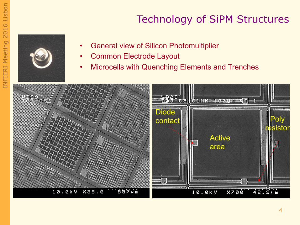
Technology of SiPM Structures
• General view of Silicon Photomultiplier • Common Electrode Layout • Microcells with Quenching Elements and Trenches
Diode contact Poly
resistor Active area
INFI
ERI
Mee
ting
2016
Lis
bon
5
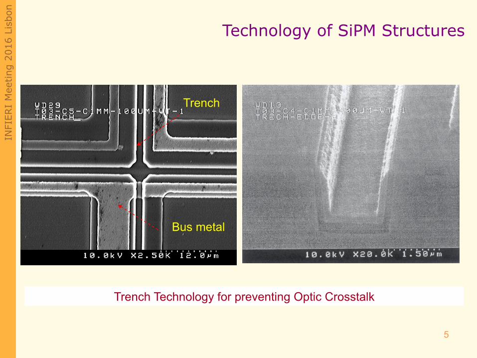
Technology of SiPM Structures
• Details of Technology
Bus metal
Trench
Trench Technology for preventing Optic Crosstalk

INFI
ERI
Mee
ting
2016
Lis
bon
6
Avalanche Breakdown pn-Junction

INFI
ERI
Mee
ting
2016
Lis
bon
7
Breakdown Mode Operation in Semiconductor
In the Avalanche Breakdown mode, the pn junction is biased above its breakdown voltage for operation; • Electrons and holes are
accelerated in the extremely High Electric Field and reach the condition of the “~ equivalent” secondary ionization for e and h;
The “Amplification Gain” is infinity, required quenching mechanism
p-region
n-region
photon
Time
Spa
ce

INFI
ERI
Mee
ting
2016
Lis
bon
8
Avalanche Breakdown pn-junction in CMOS
Standard CMOS pn-junction: – The Electric Field is Not Uniform
Required the Special Design for Uniform of the Electric Field

INFI
ERI
Mee
ting
2016
Lis
bon
9
Avalanche Breakdown pn-junction Technology
Guard Ring – Special Structures to avoid the Non Uniformity of the electric field
Unfortunately such Structures is not following the Standard CMOS Technology Rules
Avalanche Photodiodes in Submicron CMOS Technologies for High-Sensitivity Imaging
231
lattice stress caused by shallow trench isolation process (Finkelstein et al., 2006a); low PDE (Faramarzpour et al., 2008; Marwick et al., 2008), possibly due to non optimized optical stack.
As far as construction details are concerned, the essential features of a SPAD are the method of formation of the guard ring, the overall shape (i.e. circular, square, others), active area diameter and the diode junction itself. Today’s nanometer scale processes provide features such as deep well implants and shallow trench isolation (STI) that may be utilised in detector design. Additionally some custom processes provide features such as deep trench isolation, buried implants, and scope for optical stack optimisation. Even in the very first samples by Haitz and McIntyre, premature edge breakdown was addressed by an implant positioned at the edge of the junction active region, and hence the first SPAD guard ring was created. State of the art SPAD constructions can be grouped according to the method of implementation of the guard ring, as discussed in the following with the aid of Fig.2 (different constructions are discussed with reference to the different cross sections shown in Fig.2 from (a) to (f)).
P- substrate
Deep N-well
P-well P-wellP+ N+N+anode cathodeOxide
hfhf
Contact(a) (b)
P- substrate
Deep N-well
N-enhanceP+ N+N+anode cathodeOxide
hfhf
Contact
P- substrate
N-wellN-well N-well
P+ N+N+anode cathodeOxide
hfhf
Contact(c) (d)
P- substrate
Deep N-well
P+ N+N+anode cathodeOxide
hfhf
Contact
P-well
N- substrate
P- well P-enhanceN+
anodecathodeOxide
hfhf
P+ P+
www.intechopen.com
INFI
ERI
Mee
ting
2016
Lis
bon
10
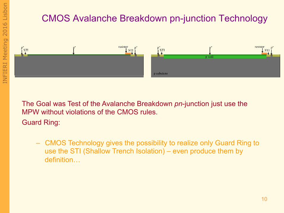
CMOS Avalanche Breakdown pn-junction Technology
The Goal was Test of the Avalanche Breakdown pn-junction just use the MPW without violations of the CMOS rules. Guard Ring:
– CMOS Technology gives the possibility to realize only Guard Ring to use the STI (Shallow Trench Isolation) – even produce them by definition…

INFI
ERI
Mee
ting
2016
Lis
bon
11
CMOS Avalanche Breakdown pn-junction Technology
TCAD SILVACO Simulation – Concentrations: native pn junction and p/nwell

INFI
ERI
Mee
ting
2016
Lis
bon
12
CMOS Avalanche Breakdown pn-junction Technology
TCAD Silvaco Simulation gives some good results – Electric field with Initial Conditions for CMOS Processess
INFI
ERI
Mee
ting
2016
Lis
bon
13
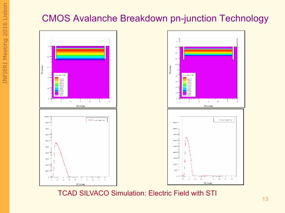
CMOS Avalanche Breakdown pn-junction Technology
TCAD SILVACO Simulation: Electric Field with STI

INFI
ERI
Mee
ting
2016
Lis
bon
14
CMOS Avalanche Breakdown pn-junction Technology
TCAD Silvaco Simulation – Ionisation Factor

INFI
ERI
Mee
ting
2016
Lis
bon
15
CMOS Avalanche Breakdown pn-junction Technology
Bias Voltage [V]0 5 10 15
I [A]
0
10
20
-1210×
/psub structure+n
/pwell structure+n
Bias Voltage [V]0 5 10 15
C [F
/mum
]
10
20
30
-1510×
/psub structure+n
/pwell structure+n
Bias Voltage [V]0 5 10 15 20
I [A]
-1110
-910
-710
-510
/pwell+n/psub+n
Bias Voltage [V]0 5 10 15
C [F
]
0
0.2
0.4
0.6
0.8
1-910×
/psub SiPM+n
/pwell SiPM+n
TCAD Silvaco Simulation and Experimental Results – Reverse IV and IC

INFI
ERI
Mee
ting
2016
Lis
bon
16
CMOS Avalanche Breakdown pn-junction Technology
TCAD Silvaco Simulation and Experimental Results – Reverse IV and IC

INFI
ERI
Mee
ting
2016
Lis
bon
• The Development and Design of Avalanche Breakdown Mode p/n Silicon Structures was performed on the basis of CMOS Multi Project Wafer (MPW).
• The results of the experimental tests show the good progress of the
implementation of the SiPM in standard CMOS technology without modification of the standard technology processes
• The goal is implementation of the electronic components in the same technological stream
Summary