design and prototype development of a wireless power
TRANSCRIPT


DUDLEY KNOX LIBRARY
NAVAL POSTGRADMONTEREY CA 65


NAVAL POSTGRADUATE SCHOOLMONTEREY, CALIFORNIA
THESIS
DESIGN AND PROTOTYPE DEVELOPMENT OFA WIRELESS POWER TRANSMISSION SYSTEM
FOR A MICRO AIR VEHICLE (MAV)
by
Robert L. Vitale
June 1999
Thesis Advisor:
Second Reader:
David C. Jenn
Jeffrey B. Knorr
Approved for public release; distribution is unlimited.


REPORT DOCUMENTATION PAGE Form Approved OMBNo. 0704-0188.
Public reporting burden for this collection of information is estimated to average 1 hour per response, including the time for reviewing instruction, searching existing data sources, gathering
and maintaining the data needed, and completing and reviewing the collection of information. Send comments regarding this burden estimate or any other aspect of this collection of
information, including suggestions for reducing this burden, to Washington Headquarters Services, Directorate for Information Operations and Reports. 1215 Jefferson Davis Highway, Suite
1204, Arlington. VA 22202-4302, and to the Office of Management and Budget. Paperwork Reduction Project (0704-0188) Washington DC 20503.'
AGENCY USE ONLY (heave blank) REPORT DATE
June 1999
REPORT TYPE AND DATES COVERED
Master's ThesisTITLE AND SUBTITLE
Design and prototype development of a wireless power transmission
system for a micro air vehicle (MAV)
AUTHOR(S)
Robert L. Vitale
FUNDING NUMBERS
7. PERFORMING ORGANIZATION NAME(S) AND ADDRESSflES)
Naval Postgraduate School
Monterey, CA 93943-5000
PERFORMING ORGANIZATIONREPORT NUMBER
SPONSORING/MONITORING AGENCY NAME(S) AND ADDRESS(ES) 10. SPONSORING /MONITORINGAGENCY REPORT NUMBER
11. SUPPLEMENTARY NOTES
The views expressed in this thesis are those of the author and do not reflect the official policy or
position of the Department of Defense or the U.S. Government.
12a. DISTRIBUTION/ AVAJLABELrrY STATEMENT
Approved for public release; distribution is unlimited.
12b. DISTRIBUTION CODE
13. ABSTRACT (maximum 200 words)
Microwave radiation at 1.0 GHz and 1.3 GHz is used to demonstrate remote powering of a micro air
vehicle (MAV). Several prototype microwave rectifier systems were fabricated in microstrip using
EEsof® computer aided engineering (CAE) software to assist in their design. Radio frequency (RF)
parameters of the rectifiers were measured on a vector network analyzer. RF-to-DC conversion
efficiency was measured for several designs and with various circuit loads consisting of lumped
elements and DC motors. A peak RF-to-DC conversion efficiency of 33 percent was achieved.
MAV antenna designs were investigated by simulating 68 geometries using the GNEC® numerical
electromagetics computer program. Two prototype MAVs were assembled, each consisting of
microwave rectifier, antenna and a miniature DC motor. It was demonstrated that a 1.8-Watt, 1.3-
GHz microwave signal could power the DC motor at free space distance of 30 inches from
transmitting antenna to prototype MAV. Greater operating distances are proposed by using higher
transmitting nnwer and antenna gain14. SUBJECT TERMS
MAV, Remotely Piloted Vehicle, Surveillance, Wireless Power Transfer,
Microwave
15. NUMBER OF PAGES
19416. PRICE CODE
17. SECURITY CLASSIFICATIONOF REPORT
Unclassified
18. SECURITY CLASSD7ICATIONOF TEDS PAGE
Unclassified
19. SECURITY CLASSD7ICATIONOF ABSTRACT
Unclassified
20. LIMITATION OFABSTRACT
ULNSN 7540-01-280-5500 Standard Form 298 (Rev. 2-89)
Prescribed by ANSI Std. 239-18, 298-102

11

DUDLEY KNOX LIBRARYNAVAL POSTGRADUATE SCHOOLMONTEREY, CA 93943-5101
Approved for public release; distribution is unlimited.
DESIGN AND PROTOTYPE DEVELOPMENT OF AWIRELESS POWER TRANSMISSION SYSTEM FOR A
MICRO AIR VEHICLE (MAV)
Robert L. Vitale
DoD Civilian
B.S., California State University Sacramento, 1985
Submitted in partial fulfillment of the
requirements for the degree of
MASTER OF SCIENCE IN ELECTRICAL ENGINEERING
from the
NAVAL POSTGRADUATE SCHOOLJune 1999


DUDLEY KNOX LIBRARYNAVAL POSTGRADUATE SCHOOLMONTEREY CA 83943-6101
ABSTRACT
Microwave radiation at 1.0 GHz and 1.3 GHz is used to demonstrate remote
powering of a micro air vehicle (MAV). Several prototype microwave rectifier systems
were fabricated in microstrip using EEsof® computer aided engineering (CAE) software to
assist in their design. Radio frequency (RF) parameters of the rectifiers were measured on a
vector network analyzer. RF-to-DC conversion efficiency was measured for several designs
and with various circuit loads consisting of lumped elements and DC motors. A peak RF-
to-DC conversion efficiency of 33 percent was achieved. MAV antenna designs were
investigated by simulating 68 geometries using the GNEC® numerical electromagetics
computer program. Two prototype MAVs were assembled, each consisting of microwave
rectifier, antenna and a miniature DC motor. It was demonstrated that a 1.8-Watt, 1.3-GHz
microwave signal could power the DC motor at free space distance of 30 inches from
transmitting antenna to prototype MAV. Greater operating distances are proposed by using
higher transmitting power and antenna gain.

VI

TABLE OF CONTENTS
I. INTRODUCTION 1
A. BACKGROUND 1
1. Wireless Power Transmission 1
2. MAV 3
B. PREVIOUS RESEARCH 5
C. OBJECTIVE 6
H. RECTIFIER CIRCUIT DESIGN 9
A. RECTIFIER CIRCUIT TOPOLOGY 10
B. MICROWAVE DIODE SELECTION 18
1. PN Junction Diode 19
2. Metal Semiconductor (MS) Diodes 20
C. PC BOARD CHARACTERIZATION 24
1. Microstrip Fabrication 24
2. Permittivity Determination Circuit (Circuit 3-1) 25
3. Permittivity Verification Circuit (Circuit 4-1) 30
D. DIODE CHARACTERIZATION 35
E. COMPUTER VERIFICATION OF SBD CHARACTERISTICS 39
F. IMPEDANCE MATCHING THE RECTIFIER CIRCUIT 42
1. Design of Shunt Stub Impedance Matching Circuit 43
2. Computer Simulations of Shunt Stub Matching Circuits 48
3. Fabrication of Shunt Stub Matching Circuits 51
4. VNA Measurement and Analysis for 1.0 GHz Rectifier Circuit
(Ckt6C2) 53
5. VNA Measurement and Analysis for 1.3 GHz Rectifier Circuit
(Ckt7d-1 and Ckt 7d-5) 55
vii
G. RECTIFIER CIRCUIT DESIGN -CONCLUSIONS 58
m. ANTENNA DESIGN 61
A. ANTENNA TYPE SELECTION 62
B. DIPOLE ANTENNA GEOMETRY 63
C. NUMERICAL ELECTROMAGNETIC CODE (NEC) MODELING OF
MAV ANTENNA (FAT DIPOLE ANTENNA) 69
1. NEC - Method of Moments Solution Description 70
2. Modeling Rules 72
3. MAV Antenna GNEC® Input Data File Development 75
4. GNEC ® Model Convergence 77
D. GNEC® SIMULATIONS TO DESIGN ANTENNA FEED 82
E. GNEC® ANTENNA RADIATION PATTERN EVALUATION 88
F. ANTENNA FABRICATION 90
G. ANTENNA INPUT IMPEDANCE MEASUREMENT 93
H. ANTENNA DEVELOPMENT CONCLUSIONS 99
IV. RECTIFIER CONVERISON EFFICIENCY MEASUREMENTS 101
A. INTRODUCTION 101
B. CONVERSION EFFICIENCY MEASUREMENT DESCRIPTION 103
1. Microwave Power Measurements 108
2. Rectified Output Average Power Measurements 110
C. CONVERSION EFFICIENCY MEASUREMENT RESULTS 1 12
D. SUMMARY OF CONVERSION EFFICIENCY RESULTS 119
1. Minimum Incident Power Requirement 119
2. Applied Microwave Power for Peak Rectifier Efficiency 1 19
3. Efficiency Decrease for Incident Power Above Peak Efficiency 119
viii

4. Multiple SBDs in Parallel Increase the Rectifier's Power Rating 120
5. Circuit Loading Affects the Rectifier Efficiency 120
E. RECOMMENDATIONS TO INCREASE CONVERSION
EFFICIENCY 122
1. Multiple SBDs in Parallel 122
2. Addition of a Load Capacitance 122
3. Impedance Match SBD Diodes at the Expected Microwave Power 122
V. OPERATIONAL DEMONSTRATION OF WIRELESS POWER TRANSFER
THROUGH FREE SPACE . 123
A. INTRODUCTION 123
B. DEMONSTRATION APPARATUS 123
1. 1.0 GHz CW Demonstration Apparatus 124
2. 1.3 GHz CW and Pulsed CW Demonstration Apparatus 129
3. RF/Microwave Radiation Exposure Limitations to Human
Personnel 133
C. MICROWAVE LINK POWER BUDGET 135
D. FREE SPACE WPT DEMONSTRATION RESULTS 138
E. CONCLUSIONS AND RECOMMENDATIONS 139
VI. SUMMARY, CONCLUSIONS, AND RECOMMENDATIONS 141
A. SUMMARY 141
B. CONCLUSIONS 141
C. SUGGESTIONS FOR FURTHER RESEARCH 142
1. GaAs Schottky-barrier Diodes 143
2. Additional Rectifier Circuit Configurations 143
3. High Powered Sources 144
4. MAV Antenna Improvements "... 144
IX

5. Improved MAV DC Motor ' 145
D. OTHER POTENTIAL INVESTIGATIONS 146
APPENDIX A. EESOF LIBRA® CIRCUIT MODEL TO DETERMINE
PERMrnVITY OF FR-4 PC BOARD 147
APPENDIX B. MICROSTRIP LINE WIDTH CALCULATIONS 149
APPENDIX C. EESOF LIBRA® CIRCUIT MODEL FOR MICROSTRIP
THROUGH LINE 151
APPENDIX D. DIODE S-PARAMETER CALCULATIONS 153
APPENDIX E. SI-SBD MODEL FILE FOR LIBRA® 159
APPENDIX F. EESOF LIBRA® CIRCUIT MODEL FOR MICROSTRIP
RECTIFIER CIRCUrr 161
APPENDIX G. WPT PROPAGATION CALCULATIONS 163
APPENDIX H. LISTING OF POTENTIAL CONDUCTIVE COATING OR THIN
FILM SUPPLIERS 169
LIST OF REFERENCES 171
INITIAL DISTRIBUTION LIST 173

LIST OF FIGURES
Figure 1. Proposed Remotely Piloted Micro Air Vehicle (MAV) 4
Figure 2. Proposed Deployment of Wireless Powered MAV 5
Figure 3. Assembled MAV, Cutaway to View Components Inside 9
Figure 4. Half-Wave Rectifier, (a) Input Signal and Rectified Output, (b)
Schematic Diagram 12
Figure 5. Full-Wave Rectifier Diode Circuit, (a) Input Signal and Rectified Output.
(b) Schematic Diagram 13
Figure 6. Full-Wave Bridge Rectifier Circuit, (a) Input Signal and Rectified Output.
(b) Schematic Diagram 14
Figure 7. Half-Wave Rectifier with Filter Capacitor, (a) Input Signal and Rectified
Output, (b) Schematic Diagram 15
Figure 8. Illustration of PN Junction Diode 19
Figure 9. Silicon Schottky-Barrier Diode (Si-SBD) Hewlett Packard Passivated
Hybrid Type 21
Figure 10. Illustration of GaAs Schottky-barrier Diode 23
Figure 1 1 . VNA Measured Return Loss for 50 ohm Microstrip Through Line
(Circuit 3-1) 27
Figure 12. Circuit 3-1 Return Loss Comparison of VNA Measurements to Libra®
Calculations using er=2.0 27
>. Circuit 3-1 Return Loss Comparison ofVNA Measurements to Libra®
Calculations using er=3.0 28
k Circuit 3-1 Return Loss Comparison of VNA Measurements to Libra®
Calculations using er=3.5 28
>. Circuit 3-1 Return Loss Comparison of VNA Measurements to Libra®
Calculations using er=4.0 29
i. Circuit 3-1 Return Loss Comparison ofVNA Measurements to Libra"
Calculations using er=5.0 '. 29
XI

Figure 17. Return Loss (Sn) 50 ohm Microstrip through Line. (Circuit 4-1: 1 1 1 mil
wide line on FR-4 PC Board), (a) Libra® Computer Simulation, (b) VNA
Measurement 33
Figure 18. Impedance Smith Chart for 50 ohm Microstrip Line. (Circuit 4-1 : 111
mils wide line on FR-4 PC Board), (a) Libra® Computer Simulation, (b)
VNA Measurement 34
Figure 19. SMT-SBD Characterization Test Fixture (Circuit 4-2) 35
Figure 20. Return and Insertion Loss for SBD Test Fixture (Circuit 4-2). (a) Libra®
Computer Simulation, (b) VNA Measurement 41
Figure 21. Shunt Stub Circuit Illustration 43
Figure 22. Smith Chart for Shunt Stub Impedance Matching of SMT-SBD Rectifier
at 1.0 GHz 46
Figure 23. Smith Chart for Shunt Stub Impedance Matching ofMAV Rectifier
Circuit at 1.3 GHz 47
Figure 24. Circuit 6x2 Return Loss for Libra® Model Variation (1.0 GHz Rectifier) 49
Figure 25. Circuit 7x1 Return Loss by Design Model Variation 1.3 GHz Rectifier
Circuit 50
Figure 26. Circuit 6C2 Return Loss Measurement Setup (1.0 GHz Rectifier Circuit) 51
Figure 27. Circuit 7d-l Return Loss Measurement Setup (1.3 GHz Rectifier
Circuit) 52
Figure 28. HP8510 Vector Network Analyzer (VNA) Return Loss Measurement
Setup 52
Figure 29. VNA Measured Return Loss of Ckt 6C2 (1.0 GHz Rectifier Circuit) 53
Figure 30. Measured and Simulated Return Loss for Circuit 6C2 (1.0 GHz Rectifier
Circuit) 54
Figure 31. Measured Return Loss and Insertion Loss for Circuit 7D-1 Circuit is
Terminated in 50 ohms and 2-Port Calibration Set Used 55
Figure 32. Simulated and Measured Return Loss for Ckt 7d-l Where Port 2 is
Terminated in 50 ohms 56
xn

Figure 33. VNA Measured Return Loss for 1.3 GHz Rectifier Circuit (Ckt 7d-l)
Without DC Motor Attached, Port 2 Configured with an Open Circuit and
with 50 ohm Termination 57
Figure 34. VNA Measured Return Loss for 1.3 GHz Rectifier (Ckt 7d-5) Port 2
Terminated with DC Motor and in 50 ohms 58
Figure 35. Dimensions for MAV Dipole Antenna 62
Figure 36. Dipole Antenna Radiation Resistance 65
Figure 37. Calculated Radiation Resistance for a Thin Wire Dipole Antenna at
Proposed WPT Frequencies 65
Figure 38. Radiation Resistance of 10.2 cm long Dipole Antenna as Thickness
Varies [Ref 15] 67
Figure 39. Reactance for a 10.2 cm long Dipole Antenna as Thickness Varies [Ref
15] 67
Figure 40. MAV Antenna Model for GNEC® Simulations, (a) Wire Frame Model.
(b) Wedge Section 76
Figure 41. MAV Antenna Impedance for GNEC® Models with 3, 5 and 9
Segments for the Source Wire Model 78
Figure 42. Currents for the Detailed GNEC® model of a MAV Antenna 80
Figure 43 . Currents for the Simplified GNEC® Model of the MAV Antenna 80
Figure 44. The Calculated Impedance ofMAV Antenna for Detailed and
Simplified GNEC® Models 81
Figure 45. MAV Antenna Resistance verses Feed Gap Size and Location Computed
using GNEC® (a) 1.0 GHz. (b) 1.3 GHz 83
Figure 46. MAV Antenna Reactance verses Feed Gap Size and Location Computed
using GNEC® (a) 1.0 GHz. (b) 1.3 GHz 84
Figure 47. MAV Antenna Impedance verses Feed Gap Size and Location
Computed using GNEC® (a) 1.0 GHz. (b) 1.3 GHz 85
Figure 48. GNEC Calculated Radiation Pattern for MAV-2 Antenna 89
Figure 49. Radiation Pattern for a Thin Dipole of Same Length as MAV Antenna 89
xin

Figure 50. Photographs of Copper Pipe MAV Antenna Disassembled to Show
Interior Connections 90
Figure 51. MAV Antennas, Fabricated from 4.4 cm Diameter Copper Pipe, (a) 1.0
GHz Version (MAV-1). (b) 1.3 GHz Version (MAV-2) 92
Figure 52. VNA Measurements on MAV Antenna 93
Figure 53. HP8510 VNA Measurement of Return Loss for MAV Antennas, (a) 1.0
GHz Version; Length 13 cm (MAV-1). (b) 1.3 GHz Version; Length 10.2
cm (MAV-2) 94
Figure 54. HP8510 VNA Measurement of VSWR forMAV Antennas, (a) 1.0 GHz
Version, Length 13 cm (MAV-1). (b) 1.3 GHz Version, Length 10.2 cm
(MAV-2) 95
Figure 55. HP8510 VNA Measurement ofMAV Antenna Impedance, (a) 1.0 GHz
Version (MAV-1). (b) 1.3 GHz Version (MAV-2) 96
Figure 56 Comparison of VSWR Calculated by GNEC and that Measured by VNA
for the 1.3 GHz MAV Antenna (MAV-2). (a) GNEC Calculation, (b)
VNA Measurement 98
Figure 57. Block Diagram of RF-to-DC Conversion Efficiency Measurement CW
Input Signal and Chip Resistor Loading 103
Figure 58. Block Diagram of RF-to-DC Conversion Efficiency Measurement,
Pulsed CW Input Signal and Chip Resistor Loading 106
Figure 59. Block Diagram of RF-to-DC Conversion Efficiency Measurement,
Pulsed CW Input Signal and DC Motor Loading 107
Figure 60. Block Diagram of Microwave Power Measurement System using the
Hewlett Packard HP8481A Thermocouple Sensor and HP438A Power
Meter [Ref 20] 109
Figure 61. MAV Rectifier Efficiency Measurements for Two Parallel Si-SBD
Microstrip Rectifier Circuit (Circuit M3-2) with External Double Short
Circuit Stub Impedance Matching Tuner, (a) 1.0 GHz CW Input Signal
with Miniature DC Motor as Load, (b) 1 .0 GHz CW Input Signal with
Miniature DC Motor as Load, (c) 1.0 GHz CW Input Signal with 10 ohm
Lumped Element Resistor as Load 1 14
xiv

Figure 62. MAV Rectifier Efficiency Measurements for two Parallel Si-SBD
Microstrip Rectifier Circuit (Circuit m4-2) with External Impedance
Matching Tuner, (a) 1.0 GHz CW Input Signal with Miniature DC Motor
as Load, (b) 1.0 GHz CW Input Signal with Miniature DC Motor as Load
(Second Data Set) 115
Figure 63. MAV Rectifier Efficiency Measurements (Circuit m7d-9) Single Si-SBD
Microstrip Rectifier Circuit with Shunt Stub Impedance Matching 1 16
Figure 64. MAV Rectifier Efficiency Measurements (Circuit m7d-8) Two Parallel
Si-SBD Microstrip Rectifier Circuit with Shunt Stub Impedance Matching 117
Figure 65. MAV Rectifier Efficiency Measurements - Expanded (Circuit m7d-8)
Two Parallel Diode Rectifier Circuit with Shunt Stub Impedance Matching
Expanded Scale showing Only Pulsed CW Input Signal Results 118
Figure 66. MAV-1 (1 GHz CW) Wireless Power Transfer Demonstration Aparatus 126
Figure 67. Wireless Power Transfer Demonstration 1.0 GHz CW Transmission
Signal to Power MAV-1 127
Figure 68. MAV-1 at the Face of the Transmitting Horn Aperature 127
Figure 69. MAV-1 Model for 1.0 GHz WPT Demonstration, (a) MAV-1 Antenna
and Rectifier Disassembled with Antenna Dimensions, (b) MAV-1
Microstrip Rectifier Circuit Dimensions 128
Figure 70. Block Diagram of Wireless Power Transfer Demonstration Apparatus
1.3 GHz CW and Pulsed CW Transmit Signals 130
Figure 71. Wireless Power Transfer Demonstration 1.3 GHz CW and Pulsed CWTransmission to MAV-2 131
Figure 72. Wireless Power Transfer Demonstration 1.3 GHz CW Transmission
Operating DC Motor to MAV-2 131
Figure 73. MAV-2 Model for 1.3 GHz WPT Demonstration, (a) MAV-2 Antenna
and Rectifier Disassembled with Antenna Dimensions Indicated, (b) MAV-
2 Microstrip Rectifier Circuit Dimensions (Circuit 7d-5) 132
Figure 74. Maximum Permissible Exposure to RF/Microwave Radiation [Ref 22].
(a) Controlled Environment Specifications, (b) Uncontrolled Environment
Specifications 134
xv

Figure 75. WPT Transmitter Power Levels for Far Field Operation of MAV.
Transmit Antenna is 15 dB Pyramidal Horn, Required Power by MAV is
15dBm 137
Figure 76. MAV-2 Required Transmitter Power verses Distance From Source
Antenna and Available AN/SPS-58 Radar Transmitter Power.
MAV_2_ave_watts is the MAV-2 Required Transmitter Power, P58A_ave
is the available AN/SPS-58 Radar Transmitter Power 140
Figure 77. EEsoft Libra® Circuit File for Sample Microstrip (Circuit 3-1) 147
Figure 78. Microstrip Width Calculations 149
Figure 79. EEsoft Libra® Circuit Model for FR-4 Microstrip Through Line 151
Figure 80. Calculations of SMT-SBD Package S parameters 153
Figure 81. EEsof Libra® Model for HP HSMS-2825 Si-SBD 159
Figure 82. EEsoft Libra® Circuit File, Microstrip Rectifier Circuit (Circuit 4-2) 161
xvi

LIST OF TABLES
Table 1. Diode Characteristics for Hewlett Packard HSMS-2825, RF Silicon
Schottky-barrier Diode , 22
Table 2. Microstrip Design Constants 45
Table 3. Smith Chart Determined Lengths and Positions for Shunt Stub 45
Table 4. Design Variation Simulations for the Shunt Stub Impedance Matching
Circuit 48
Table 5. GNEC® Model Parameter Guidelines 74
Table 6. Acceptable Ranges for GNEC®/NEC 4.1 MAV Geometry Definitions 75
Table 7. GNEC® Model Wire Segment Definition 76
Table 8. GNEC® Calculated Reactance and Impedance for 10.2 cm MAV Antenna
Operating at 1.0 GHz. (a) Reactance, (b) Impedance Magnitude 86
Table 9. GNEC® Calculated Reactance and Impedance for 10.2 cm MAV Antenna
Operating at 1.3 GHz. (a) Reactance, (b) Impedance Magnitude 87
Table 10. Summary of Feed Gap Parameters for Optimized 10.2 cm MAV Antenna 88
Table 11. Summary of Rectifier Efficiency Measurements 112
Table 12. Far Field Operation Specifications for WPT ofMAV Demonstrators 136
Table 13. MAV WPT Demonstration Summary 138
Table 14. AN/SPS-58 Air Search Radar Transmitter Specifications 139
Table 15. Conductive Coating Suppliers for Carbon Fiber MAV Body 169
xvn

XV111

ACKNOWLEDGMENTI would like to extend my sincere gratitude to my thesis advisor, Professor David
Jenn, for the opportunity to learn new engineering skills and the chance to apply them on a
truly unique project, a project that obtained high visibility if not much funding. Professor
Jenn's guidance and especially his patience were appreciated as completion of this thesis
was delayed several times due to workload levels in the Microwave Lab.
I also extend a special thanks to Professor Jeffery Knorr, who as my faculty
supervisor, has been one of my chief mentors since I arrived at the Naval Postgraduate
School. Professor Knorr and my direct supervisor, the ECE Lab Manager, Mr. Bob
McDonnell have been very supportive of my efforts to achieve a Masters degree from this
institution. Many supervisors would not be as supportive and I sincerely thank them both.
I also thank Eric Conner from the Physics department for his assistance in etching
the microstrip boards and Dr. Jovan Lebaric for suggestions made towards the rectifier
circuit design. A sincere thanks is extended to the engineering students in the classes that I
have assisted. The drive and commitment displayed by these students inspired me to
continue with this work. I learned as much from them as they did from me.
Lastly and foremost, I extend my sincerest gratitude to my wife, Dr. Theresa
Repasky. Her love, support and understanding while I spent long hours working on this
project and preceding coursework were especially appreciated.
xix

I. INTRODUCTION
A. BACKGROUND
1. Wireless Power Transmission
Wireless Power Transmission (WPT) refers to the point to point transfer of electrical
power in space without the use of transmission lines. All radio applications presently do
this; however, they only transfer very small amounts of power. WPT seeks to transfer
significant amounts of energy, which would be used to power remote systems. Such
systems include remote sensors and even the propulsion of vehicles. This thesis investigates
the possibility of using WPT to power a tiny remotely piloted micro air vehicle (MAV).
Wireless power transmission for remote powering of aerospace vehicles has its
origin in research conducted by Brown in 1963 [Ref 1]. This research was an outgrowth of
a Defense Advanced Research Projects Agency (DARPA) project to develop high power
microwave tubes. At that time, Brown was able to develop microwave to DC conversion
using closed spaced thermionic diodes in a flat array that provided 50% RF-to-DC
conversion efficiency and produced over 900 watts of DC power [Ref 2]. The work
culminated with a demonstration of a tethered wireless powered helicopter in 1964.
Although this demonstration was impressive, the application of WPT to an airborne vehicle
was ahead of its time. Technology in the mid 1960s did not allow sensors small enough to
be carried by the helicopter and, in addition, the diode array antenna required for operation
was many times larger than the helicopter itself. Although Brown's initial research was

funded by DARPA, much of the follow on research was funded internally by Raytheon
Corporation or was conducted at his own expense.
Since the initial research, much of the subsequent work on wireless power transfer
has concentrated on space based applications. These applications include the NASA solar
power satellite, which has the objective of collecting solar energy in space for use on Earth.
Energy collected in space would be transmitted to Earth ground stations via a high power
microwave signal, then rectified and used in the power grid. Other WPT space projects
included electrical power transmission from remote nuclear powered satellites (generators)
to a space station, remote power sources for spacecraft propulsion systems (ion thrusters),
and the powering or recharging of miniature satellites from Earth [Ref 3]. The last
application has recently shown to have promising practical use. Providing Earth based
electrical power to an orbiting space satellite would greatly reduce the size and, more
importantly, the launch weight of a satellite, thereby vastly reducing the cost to build and
launch the satellite.
Recently, three separate university research groups have been working on the
application of WPT to power remotely operated air vehicles. The Kobe University (Japan)
has successfully demonstrated WPT to an airship using large flat panel arrays (Project
ETHER) [Ref 4]. The University of Alaska at Fairbanks is in the process of developing a
model helicopter powered via WPT (Project SABER) [Ref 5]. Project SABER re-uses a
diode array originally built by Brown. Finally, the Naval Postgraduate School has
participated in the development of a remotely powered micro air vehicle (MAV) in

cooperation with the Lutronix Corporation [Ref 6]. WPT techniques to support remote
powering or remote recharging of a miniature rotorcraft are the subject of this thesis.
2. MAV
The micro air vehicle (MAV) is intended to be a miniature (maximum size of
several inches) airborne remotely piloted rotorcraft. MAV missions generally fall into two
categories. The first is indoors, where the ranges may be short but mission duration long
(perhaps days). The second is outdoors, where the operational ranges are longer and the
aerodynamic environment more severe. Typical outdoor MAV missions include the ability
to fly out to ranges of several kilometers, conduct surveillance or possibly detonate a charge
to destroy a target in a suicide mission.
One important indoor application is the video surveillance of building interiors,
where people are not allowed or physically cannot go. Examples include buildings that are
controlled by unfriendly personnel (such as terrorists), areas or situations that are
environmentally dangerous (such as inside a nuclear reactor) or perhaps where it is more
economical to use robotic surveillance. Because of its small size and quietness due to
electrical propulsion (i.e. covertness), the MAV is thought to have greater success flying
against interior building targets rather than flying outside, where wind forces tend to favor
the aerodynamics of a larger air vehicle.
A micro air vehicle under development by Lutronics Corporation is shown in
Figure 1. This MAV is presently electrically powered via a tether cable. However, to
become practical for most applications, it will need to carry an energy source or receive
electrical power via WPT. MAV operations using WPT could eliminate a large percentage

of the vehicle's weight, namely the fuel and its tank or the battery. Weight and space
savings would permit the MAV to operate on extended missions and be better equipped
since additional space and weight are available for sensors, flight control systems and
weapons. Even if WPT only supplied battery recharge power, the battery could be made
smaller and lighter without adversely affecting mission endurance because the vehicle could
be recharged intermittently in-flight.
flight configuration
Figure 1. Proposed Remotely Piloted Micro Air Vehicle (MAV)

B. PREVIOUS RESEARCH
The tradeoffs involved in the design of a remotely piloted vehicle have been
discussed in several publications [Ref 7, 8]. One possible approach is to use several ground
stations that are synchronized to provide a coherent "spot" at the MAV as illustrated in
Figure 2. This multiple ground station approach allows a deployment that is more flexible
and is more robust in the presence of propagation obstructions than a single ground station.
Coherent
Beam Spot
Ground
Stations
Walls and
Obstructions
Figure 2. Proposed Deployment of Wireless Powered MAV
Previously, Gibson [Ref 9] conducted investigations with regard to propagation
losses due to building walls and evaluated several antenna approaches. Propagation
measurements and computer simulations were conducted for frequencies from 2 to 6 GHz.
In particular, the signal attenuation through building walls was modeled and verified by
measurement. Data showed a trend of improved microwave signal propagation through
buildings as the frequency decreased.
The selection of frequency is a critical issue. Although lower frequencies have a
better capability to penetrate buildings, the antenna size for the required gain becomes
prohibitively large. Therefore, it appears that 1 GHz is about the limit at the lower end.

A transmission frequency of 2.45 GHz was suggested by Gibson; however, it will be
shown in Chapter HI that a dipole antenna the size of the MAV would have a very large
radiation resistance and makes impedance matching of the rectifier circuit to antenna
difficult. The frequency chosen for this research was 1 GHz, which for the MAV body size
provides a radiation resistance value close to the characteristic impedance of the interfacing
transmission line. Subsequent research increased the WPT frequency to 1.3 GHz in order to
use the high transmit power of the AN/SPS-65 air search radar located in the Naval
Postgraduate School's Radar Laboratory.
C. OBJECTIVE
The objective of this research is to develop a prototype of a MAV that is powered by
WPT from an off-board energy source. The dimensions of the model are the same as the
flying model built by Lutronix. There were two major tasks. The first was to design an
antenna with the proper coverage and input impedance, with little or no weight penalty. The
second task was to design an efficient rectifying circuit that would provide sufficient current
to a DC motor.
This thesis consists of six chapters. Chapter II discusses the design and fabrication
of the microstrip rectifier circuit, including the computer simulations conducted using EEsof
Libra . Verification of the circuit design is accomplished using measurements from the
Hewlett Packard HP 85 IOC Vector Network Analyzer System. Chapter III covers the
development of the mockup MW body that serves as the receiving antenna for WPT.
Chapter in includes computer modeling of the antenna using the method of moments,
Numerical Electromagnetics Code (NEC 4.1), verification measurements on the vector

network analyzer system, and also describes how the various MAV antenna designs were
fabricated. Chapter IV presents the efficiency testing that was conducted on several
microstrip rectifier designs and explains the techniques used to measure RF-to-DC
conversion efficiency. Efficiencies were measured for continuous wave (CW) signals and
for a simulated radar waveform (pulse modulated CW). Chapter V presents test results of
the entire MAV WPT system using CW and pulse modulated CW signals that simulated the
Naval Postgraduate School's AN/SPS-65 air search radar. Finally, Chapter VI presents
conclusions of the effort along with some suggestions for possible future research.


II. RECTIFIER CIRCUIT DESIGN
The wireless power transfer system on the MAV consists of two basic parts: the
receiving antenna and the microwave rectification circuitry. Independent development of
the rectifier and antenna was possible by impedance matching each of these elements to a
short piece of 50 ohm RG-141 semi-rigid coaxial cable. This short (1.2 inches) semi-rigid
cable served as the feed from the antenna to the rectifier circuit and also provided a rigid
mount for the circuit and motor inside of the top half of the MAV. An illustration of the
assembled MAV is shown in Figure 3, where the microwave rectifier circuit is located
inside the top half of the MAV dipole antenna. This chapter discusses the design,
development and verification testing of the microwave rectification circuit and the unique
aspects of its design for efficient operation at microwave frequencies.
DC Motor
Microstrip
Rectifier Circuit
Antenna Feed Gap
Upper Section of Dipole
Antenna
Rigid Coaxial Feedline
Lower Section of Dipole
Antenna
Figure 3. Assembled MAV, Cutaway to View Components Inside.

A. RECTIFIER CIRCUIT TOPOLOGY
The MAV body serves as the antenna, receiving a zero average voltage sinusoidal
signal, continuous wave, at microwave frequencies. The received microwave radiation is
converted using a microstrip rectifier circuit to a signal with an average DC voltage. This
DC voltage is used to drive a miniature DC motor, which spins the helicopter rotor blade.
The goal of the rectifier circuit is to provide the largest average DC power for a given input
microwave signal power. This section discusses the types of rectifier circuits investigated
and how a circuit selection was accomplished.
Rectification of microwave power has unique design challenges relative to the more
commonly encountered problem of rectification of 60 Hz power signal. The unique
challenges include: (1) requirements for quick switching, (0.1 ns), to keep up with the signal
frequency; (2) compensation for parasitic reactance, resistance and circuit topologies (such
as lead lengths and transmission structures) that are not a factor for lower frequency
operation; (3) effective blocking of the reverse current on the negative half cycle; and (4)
high frequency impedance matching to avoid reflection of the received CW power at the
antenna terminals.
Three rectifier circuit topologies are typically used for passive diode rectifiers. They
are: (1) half-wave rectifier, (2) full-wave rectifier, and (3) full-wave bridge rectifier.
Figure 4, Figure 5 and Figure 6 illustrate these three circuits and their computer simulated
rectified output voltages using for a sinusoidal input signal. Computer simulations were
conducted using Pspice. Upon inspection of the simulated output voltage, it is noted that
none of these circuits provides a true DC voltage. Rather, the rectifier circuits convert a zero
average sinusoidal voltage signal to a non-zero average voltage time varying signal.
10

A rectifier's efficiency, or ability to provide a larger average output voltage, can be
increased by placing an appropriately sized capacitor across the rectifier output in parallel
with the load. This is illustrated for a half-wave rectifier in Figure 7. This "filter" capacitor
serves to reduce voltage variations in between positive voltage swings at the rectifier output.
11

10U~
5U-i
-5U-
-10U +6*»us 66US 68us
|U(Rload:2) « U(fintenna:*)70us
Tine
72us 74us 76us
(a)
Antenna
D1
(
<y)
1S Rload
(b)
Figure 4. Half-Wave Rectifier,
(a) Input Signal and Rectified Output, (b) Schematic Diagram.
12

10U-
5U
OU
-5U
:^^•. V9''2'8"voT'is.
j>mS-
"Load Vol tage".
" 'I
Antenna Vol tage
/
-10U+--64us
_W_
!U2
66us 68us(Rload) U(Rs:1)- U(Antenna:-)
7 0us
Time
V.
72us 76us
(a)
Rs
Antenna
XMFR1 J \r
w-tD5
D6
£>H
<>
Rload
\7,
(b)
Figure 5. Full-Wave Rectifier Diode Circuit,
(a) Input Signal and Rectified Output, (b) Schematic Diagram.
13

-10U + -
64us 66us 68US 70USFjU(Rload:2,Rload:1) U(Antenna:+)
Tine
72us 74us 76us
(a)
(b)
Figure 6. Full-Wave Bridge Rectifier Circuit,
(a) Input Signal and Rectified Output, (b) Schematic Diagram.
14

10U
5U
OU
-5U-i
-10U +6Uus 66us 68usi°iU(Rload:2) U(flntenna:*)
7 Bus
Tine
72us 74us
(a)
D1
>RloadAntenna
(nt) filter C
f
w
(b)
Figure 7. Half-Wave Rectifier with Filter Capacitor,
(a) Input Signal and Rectified Output, (b) Schematic Diagram.
15

The output voltage when the diode is not conducting' is compensated for by the
discharge of the filter capacitor. It can be expressed as
v (t)=Vp e-tIRC
(1)
where Vp is the peak voltage of the rectified signal, R is the load resistance and C the filter
capacitance.
The output voltage deviation (ripple) from the peak voltage can be derived by taking
the discharge time (t) to be a full period \T) of the input sinusoid and equating this voltage
ripple to the difference between peak (Vp ) and minimum ripple voltage (Vr ) [Ref 10]. For
RC» T , the exponential can be approximated by the series (l - ypr j and the minimum
output voltage can be expressed as
V =V( T ^1-
^RC
(2)
The output DC voltage is approximated by the average voltage between the peak
(Vp ) and voltage minimum (V0min )
V =V\
V
(3)2fRC
Equation (3) was developed for the half-wave rectifier. The same method can be
applied to the full-wave rectifier using 772 for the discharge time. The resulting
expression for the output voltage becomes
(1 ^
V =V 1
4fRC(4)
16

Equations (3) and (4) show that the larger average voltage of the full-wave rectifier can be
approached by the half-wave rectifier with the filter capacitor doubled.
The filter capacitor does, however, increase the forward diode conduction current.
This current, in addition to the normal load current, is required to recharge the filter
capacitor and is given by
^ D forward * L
( \lRC^1 + nA
V T^ J
(5)
where lL is the load current and the second term of equation (5) is due to the filter
capacitance [Ref 10]. The increased conduction current occurs when the diode is forward
biased and provides the upper limit of the filter capacitance. Generally it is desired that
RC» T to increase output voltage. However if RC is made too large, the conduction
current will exceed the current rating of the diode. For example, if RC = 10T , the forward
conduction current through the diode becomes 15 times the normal load current (lL ).
The half-wave rectifier has several advantages over the full-wave rectifier and full-
wave bridge circuits for microwave signal rectification. The greatest advantage is the
simplicity of circuit layout and ease of fabrication as a microstrip structure. All components
reside on one side of the microstrip media with a minimum number of via holes (conductive
paths from the top microstrip plane to the lower ground plane). This is important since via
hole positioning and via hole reactance introduce errors into the impedance matching
process. Also, the half-wave rectifier has a forward voltage drop across only one diode
(Vd ) whereas for the full-wave bridge rectifier, the forward voltage drop occurs across two
17
diodes in series and is, therefore, doubled {2Vd ). For these reasons the half-wave rectifier
circuit of Figure 4 was chosen for the microwave rectification circuit.
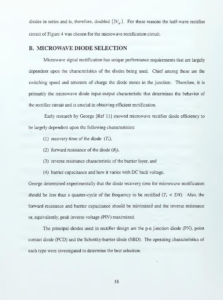
B. MICROWAVE DIODE SELECTION
Microwave signal rectification has unique performance requirements that are largely
dependent upon the characteristics of the diodes being used. Chief among these are the
switching speed and amounts of charge the diode stores in the junction. Therefore, it is
primarily the microwave diode input-output characteristic that determines the behavior of
the rectifier circuit and is crucial in obtaining efficient rectification.
Early research by George [Ref 11] showed microwave rectifier diode efficiency to
be largely dependent upon the following characteristics:
(1) recovery time of the diode (7V),
(2) forward resistance of the diode (Rf),
(3) reverse resistance characteristic of the barrier layer, and
(4) barrier capacitance and how it varies with DC back voltage.
George determined experimentally that the diode recovery time for microwave rectification
should be less than a quarter-cycle of the frequency to be rectified (Tr < T/4). Also, the
forward resistance and barrier capacitance should be minimized and the reverse resistance
or, equivalently, peak inverse voltage (PIV) maximized.
The principal diodes used in rectifier design are the p-n junction diode (PN), point
contact diode (PCD) and the Schottky-barrier diode (SBD). The operating characteristics of
each type were investigated to determine the best selection.
18

1. PN Junction Diode
The PN diode is commonly used for low frequency detection and rectification. A
diagram of the PN diode is shown in Figure 8. The forward biased p-n junction will
typically have two types of forward bias capacitance: depletion layer capacitance (CJ) and
diffusion capacitance (Q). Q is due to majority charge carriers crossing the p-n junction
and becoming minority carriers in the other semiconductor material. These minority carriers
do not recombine immediately and if the bias reverses before recombination occurs, then
these carriers return across the junction as a current pulse. This effect is called the junction
storage capacitance and is a problem for operation at high frequencies since the signal is not
effectively rectified due to the reverse current from the junction storage capacitance.
Therefore the PN diode does not operate well as a rectifier at microwave frequencies.
—N
—
Anode Q Contact metalv Q Cathode
(Au, Ag typical)
Figure 8. Illustration of PN Junction Diode.
19

2. Metal Semiconductor (MS) Diodes
The point contact diode (PCD) and Schottky-barrier diode (SBD) are metal-
semiconductor (MS) diodes. This terminology refers to a type of device physics where the
rectifying junction is metal to semiconductor rather than semiconductor to semiconductor
(such as the PN diode). The difference between the PCD and SBD is in their construction.
In the case of the SBD, Schottky-barrier metal is deposited onto the semiconductor as part of
the chip fabrication process, whereas in the PCD, the barrier metal is at the pointed end of a
whisker, which is mechanically wedged against the semiconductor chip during final
assembly. The prudent choice for the MAV rectifier is the SBD. Mechanical vibrations
and shock are likely to be typical in this operating environment and the mechanical PCD
whisker contact may not be reliable for this application.
Since the PCD and SBD are MS diodes, they operate on similar electronic
principals. Therefore discussing the electronic operation of the SBD applies as well to the
PCD and helps to demonstrate an inherent advantage of a SBD microwave rectifier circuit.
The SBD consists of a metal semiconductor junction where the Schottky-barrier metal is
different than the metal used to make the contacts and forms the anode of the diode. A
diagram of a Hewlett Packard passivated hybrid SBD is shown in Figure 9.
20

Si02- passivation layer
limits SB metal area
Anode Schottky-barrier metal
SZ.diffused p-type ring,
eliminates premature
breakdown of passivated
diode, keeping C, low
(lpF min)
Contact metal
(Au, Ag typical)
Figure 9. Silicon Schottky-Barrier Diode (Si-SBD)
Hewlett Packard Passivated Hybrid Type.
A metal-semiconductor diode involves majority carriers only; minority carriers are
non-existent due to the lack of oppositely doped semiconductor. Forward conduction
current consists of the majority carriers flowing into the Schottky-barrier metal (anode) from
the semiconductor (cathode). Unlike the p-n type semiconductor junction, the Schottky-
barrier does not have minority charge storage and the resultant diffusion capacitance (Q).
This makes the SBD well suited for high frequency operation because the SBD has only one
capacitive effect: depletion-layer capacitance (C, ) [ReflO].
The SBD selected for use in the MAV rectifier circuit is the Hewlett Packard
HSMS-2825, which has a single housing that contains a pair of SBDs with silicon substrate
and is packaged as a surface mount technology (SMT) device. The HSMS-2825 SMT-SBD
pair are arranged unconnected, in parallel and in the same direction. This arrangement
simplified assembly onto the microstrip structure and provided the option of using multiple
diodes in parallel to increase the current carrying capability of the rectifier. The SMT
package provided a compact design that minimizes lead length, which is helpful for
21

impedance matching. SMT devices are difficult to hand solder, requiring a microscope,
tweezers and a steady hand, but their size advantage make up for their assembly difficulties.
Individual SBDs in this package have the characteristics shown in Table 1. If the
recovery time is defined as the RC time constant, the HSMS-2825 has a Tr
of lOps.
George's Trspecification for a 1.3 GHz microwave signal is 190 ps, which is compatible
with the HSMS-2825 SBD.
Name Characteristic Value
VBr PIV- peak inverse voltage
(minimum diode breakdown voltage)
8V
vF maximum forward voltage 340 mV
h reverse leakage current 100 mA
CT maximum capacitance 1.0 pF
Rd typical dynamic resistance 10 ohms
Table 1. Diode Characteristics for Hewlett Packard HSMS-2825,
RF Silicon Schottky-barrier Diode.
22
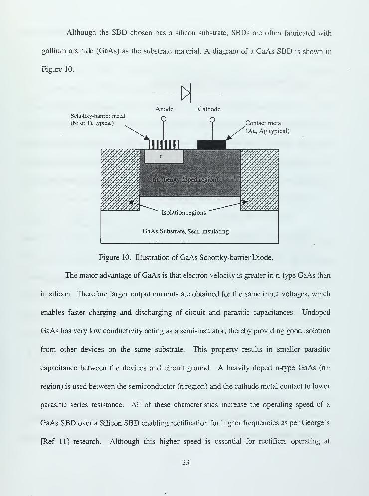
Although the SBD chosen has a silicon substrate, SBDs are often fabricated with
gallium arsinide (GaAs) as the substrate material. A diagram of a GaAs SBD is shown in
Figure 10.
Schottky-barrier metal
(Ni or Ti, typical) ^Contact metal
(Au, Ag typical)
Isolation regions
GaAs Substrate, Semi-insulating
Figure 10. Illustration of GaAs Schottky-barrier Diode.
The major advantage of GaAs is that electron velocity is greater in n-type GaAs than
in silicon. Therefore larger output currents are obtained for the same input voltages, which
enables faster charging and discharging of circuit and parasitic capacitances. Undoped
GaAs has very low conductivity acting as a semi-insulator, thereby providing good isolation
from other devices on the same substrate. This property results in smaller parasitic
capacitance between the devices and circuit ground. A heavily doped n-type GaAs (n-i-
region) is used between the semiconductor (n region) and the cathode metal contact to lower
parasitic series resistance. All of these characteristics increase the operating speed of a
GaAs SBD over a Silicon SBD enabling rectification for higher frequencies as per George's
[Ref 11] research. Although this higher speed is essential for rectifiers operating at
23
millimeter wavelengths [Ref 12], it is not critical for the frequencies used in this research
(1.0, 1.3 GHz). Therefore the speed of GaAs was not considered necessary.
C. PC BOARD CHARACTERIZATION
Microstrip transmission line was chosen to be the transmission medium for the
rectifier circuit because design and fabrication were more efficient as opposed to other
types of transmission structures such as stripline. Microstrip structures can be fabricated
using printed circuit board etching methods, whereas other appropriate guiding structures
(such as stripline) require precision machining of dielectric materials and fixtures and
would have incurred greater costs to fabricate.
Design of the microstrip circuit pattern required accurate knowledge of the relative
permittivity (£r) of the FR-4 dielectric substrate. Since this particular PCB is typically used
for low frequency applications, accurate information for eTwas not available and its value
was experimentally determined. Experiments consisted of fabricating an unbroken through
transmission line on a sample PCB (Circuit 3-1), measuring its scattering parameters on a
vector network analyzer, and then using computer simulations to adjust eT
so that the
measured and simulated scattering parameters matched. A 50 ohm through microstrip line
(Circuit 4-1) was then designed, fabricated and tested to verify the validity of the er
determined previously.
1. Microstrip Fabrication
The printed circuit board (PCB) material was purchased pre-coated with photo-
resist. This PCB material was 1/16 inch thick fiberglass epoxy with 1 ounce copper plating
24

on both sides, commonly referred to as FR-4 PCB. Fabrication of the rectifier microstrip
traces was done by photodeveloping and ferric cloride etching. This process exposes the
PCB to high intensity ultraviolet (UV). light filtered through a pattern of the microstrip
(circuit mask). The UV light burns off photo-resist in the areas where the copper is to be
removed. A developer solution is applied to the board, which adheres to the photo-resist,
coating desired areas of copper (traces). The board is emerged into a bath of ferric chloride
to dissolve copper plating from regions unprotected by the developer coating. The ferric
chloride bath is heated and agitated to increase effectiveness and shorten etching time. The
etched board is removed from the bath, rinsed with water and the developer removed from
the copper traces by hand using a non-metallic abrasive pad.
2. Permittivity Determination Circuit (Circuit 3-1)
A microstrip through line circuit of width 160 mils (0.001 inch) and length 4775
mils was fabricated using FR-4 PCB material. This microstrip circuit was labeled
Circuit 3-1. A Hewlett Packard HP8510C Microwave Vector Network Analyzer System
(VNA) was used to measure input impedance (Zin ) , return loss (Sj
x ) and insertion loss
(S 2 \ ) of the through microstrip line (Circuit 3-1). A copy of the return loss as measured by
the VNA is shown in Figure 11.
A computer model of this microstrip transmission line was developed using EEsof
Libra" high frequency circuit simulation software. This model is attached as Appendix A.
The computer model had the same geometry and dimensions as the fabricated microstrip
line, complete with the SMA connectors on both ends. Simulations using the Libra model
were conducted and the relative permivitty (er ) of the substrate adjusted until the return
25

loss (Sn ) of the simulations agreed with the VNA measurements of Su . Libra® calculated
and VNA measurements of Su were considered to agree when the number and frequency
separation between Sn minimums (or nulls) matched and the overall return loss magnitudes
were nearly the same. A frequency offset between the Libra® calculated and measured
return loss plots was expected. This offset is due to uncertainties in the location of the VNA
calibration plane reference which resulted from using the VNA calibration set (open, short,
load) without entering the calibration set characterization data into the VNA computer
memory.
An early evaluation of the Libra® model computation verses the VNA
measurements determined a value for erof 4.8 for the FR-4 PC board substrate. This value
(er=4.8) was then used in later designs of the microstrip rectifier.
Further review after the rectifier circuits were fabricated and tested uncovered an
error in the determination of the value used for relativity permittivity (£r=4.8) . Libra®
calculations of return loss for Circuit 3-1 using values of 2.0, 3.0, 3.5, 4.0 and 5.0 for eT
were redone and plotted alongside the VNA measurements. These plots are shown in
Figures 12 to 16. Comparisons of these figures show that the agreement occurs for when the
Libra® calculation uses an erof 3.5, which is shown in Figure 14. Although this error does
affect the subsequent rectifier circuit design, the initial circuit performance was acceptable
so that a circuit redesign and fabrication was not required. The use of a high quality
microwave substrate would eliminate the potential for this error, since the material
characteristics would be known and controlled.
26

REF 0.0 oBlog MOG
5.0 dB/-17.243 dB
VMRR I CRT 3-i
'41
/ \
\/\
/^
IS
ST«RTSTOP
l^RREFTT1.03 GHz-15. 124 dE
MRRKER 21.4B GHz-38.518 dE
MARKER 31.85 GHz-18.193 c
MRRKER 42.225 GHz39.889 dB
»MfiRKER 52.59 GHz17.243 dB
0.800000000 GHz2.800000000 GHz
09 JUN 96;14:27:49
Figure 11. VNA Measured Return Loss for 50 ohm Microstrip Through Line (Circuit 3-1).
Frequency (MHz)
00 ON1080 1220 1360 1500 1640 1780 1920 2060 2200 2340 2480 2620 2760
u
-10 -
,.-
-20-'--jff »
£5-30,
' \l \l ' •'
-40 -
:; :
-50 -
:.'''
•;
*
..... ..
-ou
Libra Er=2.0
Figure 12. Circuit 3-1 Return Loss Comparison of®VNA Measurements to Libra Calculations using e
r- 2.0
27

Frequency (MHz)
oooooooooooooOOOOCMVOO^OOCN'OO'^-OOCSSOOOCv — — — — — — — CMCNC-JrJfNCN
-50
-60
-70
miTTTni iTmrrinm rr mmmim: iiiinnniiiiiiiiiiii
VNA Measurement
Libra Er=3.0
Figure 13. Circuit 3-1 Return Loss Comparison of
VNA Measurements to Libra" Calculations using sr=3.0
8 §00 Ov
Frequency (MHz)
OOOQOOOOQOOOOOOfSvOO-^OOfN^OOTOOCJOOfsromvor— ©v o rj m * \o r~
u -
-10-
-20-
S* -30-
-40-
-50 -
/•'*
s \ / '" \ ' /
V ' 'V
\,
..... ..VNA Measurement
Libra Er=3.5
-ou
Figure 14. Circuit 3-1 Return Loss Comparison of®VNA Measurements to Libra Calculations using e
r= 3.5
28

8 §OO 0>
Frequency (MHz)
OOOOOOOOQOOOCoofNsoo-fl-oorjvoO'trootMvc >
i
-10-
-20-
Mar -30-
-40 -
-50-
--""** ***^**-.
:
: V ''•
\l
'••
-60 J
Libra Er=4.0
Figure 15. Circuit 3-1 Return Loss Comparison of®VNA Measurements to Libra Calculations using e
r= 4.0
Frequency (MHz)
>
800 9401080 1220 1360 1500 1640 1780 1920 2060 2200 2340 2480 2620 2760
\j
-10-
*' ^j—-*!^ ^^^^^^^ * \ _ *
-20- \ ^V •* * 7\ <^^* ^***\i
/ ' \ / \
£f -30- I W \ / \ i
\ / •'
-40 -',
v
-50-
^fi --ou
Libra Er=5.0
Figure 16. Circuit 3-1 Return Loss Comparison of
VNA Measurements to Libra® Calculations using er= 5.0
29

3. Permittivity Verification Circuit (Circuit 4-1)
The FR-4 PCB material substrate relative permittivity (sr ) determined from the
early Circuit 3-1 experiments was used to design a FR-4 microstrip transmission line with
characteristic impedance (Z ) of 50 ohms. This circuit was labeled Circuit 4-1 and served
to test the estimated value of the permittivity of the FR-4 substrate material. The design
parameters for a microstrip transmission line are: (1) microstrip line width (w), (2) dielectric
substrate thickness (d), and (3) relative permittivity or relative dielectric constant [e r ) of the
substrate. These parameters can be adjusted to achieve a desired transmission line
impedance (Z ) using the following formulas [Ref 13]:
w %e'
d e2.4
vv_ 2
d n5-l-ln(25-l) +
e-l (
2e.ln(5-l)+0.39
0.6\\
yj
wfor — <2
d
wfor— > 2
d
(6)
(7)
where
60
Zn e+\ e.-l (+
B =
2 £r+l
377 7T
2Z V^T
0.23 +0.11
\
(8)
(9)
A 50 ohm microstrip through line was designed and fabricated to verify the value of
srand the design equations. This structure, labeled Circuit 4-1, used FR-4 PCB material
with a thickness of 62.5 mils (1 mil = 1/1000 inch) and was designed using (6) for an
30

assumed fr of 4.8. Calculations yielded a microstrip width of 111 mils. These calculations
are attached as Appendix B.
A check on these calculations used [Ref 13]
7 60iZ =— In
£
fSd w \+
—
w 4dj
(10)
where ee
is the effective permittivity of the microstrip structure, given by
^ e £effective
£ r + 1 £ . - 1— + —
11 + 12 —w
(11)
The impedance calculated using (10) and (11) was 50.4 ohms which is 0.8% error from the
design impedance of 50 ohms.
Return loss (Su ) and input impedance for Circuit 4-1 was measured using the
HP8510 VNA. Circuit 4-1 was also modeled and simulated using EEsof Libra®. This
model is attached as Appendix C. Comparison of return loss (Sn) between the Libra®
computer simulations and VNA measurements are shown in Figure 17a and Figure 17b.
Smith Chart plots of input impedance for Circuit 4-1 are shown by Figure 18a (Libra®
Simulation) and Figure 18b (VNA Measurement).
The envelope of the simulated and measured return losses generally agree over the
frequency band investigated (0.8 to 2.5 GHz). However, the locations of the minima and
maxima were shifted in frequency. The disagreement of return loss maxima and minima
with respect to frequency can be attributed to measurement inaccuracies of line length and
the load plane location error during VNA calibrations. This load plane error is the result of
31

using coaxial short, open, and wideband load (50 ohms) calibration as opposed to a through,
reflect line calibration. The plot of input impedance for Circuit 4-1, as shown on the Smith
Charts of Figure 18a and Figure 18b, indicates that microstrip through line of width 111 mils
has an impedance very close to 50 ohms. The difference for Circuit 4-1 is likely due to
manufacturing tolerances for a microstrip circuit where the permittivity of the substrate
material (fiberglass epoxy) is not tightly controlled and may vary considerably between
different boards.
32

EEsof - Libra - Mon Nov 9 11:05:39 1998 - ckt4-l
rj DB[S11]
CKT4-1
+ DB[S21]
CKT4-1
0.000
^/
7^~^1
rf ° S
\ / \ i
-25. 00
\ /\
\
/
/ \ /
\r1
\ /' if
k 1 1
ti~
\
1
i
-50. 00 _ i1
0.800 1.800 FREQ-GHZ 2 800
(a)
REF 0.0 oBA 5.0 oS-'V -48.906 cB
log M«GR3= K.K r.!b
5.53 (Si.
W89G
W5RKER" 1 ~"|
.1.0 GHz-as. 925 oS
morker a ;
1.3 GHz-25.254 dB
I
!MPIRKER 3 !
il.14 GHz|
•23.925 oS
MPRKER A1.52 GHz,-48.906 oS
26 OCT 3§|_14:_42:51j
(b)
Figure 17. Return Loss (Sn) 50 ohm Microstrip through Line.
(Circuit 4-1: 1 1 1 mil wide line on FR-4 PC Board).,®
(a) Libra Computer Simulation, (b) VNA Measurement.
33

EEsof - Libra - Mon Jun 15 14:59:02 1998 - ckt4-l
Sll
CKT4-1
fi: 0.80000
f2: 2. 800C0
.2 .5
(a)
REF 1.0 Units5 200.0 mUnit.S''V 49.949 n 0.1211 n
MARKER 1
1.15 GHz55.S21 n
-3.6855 fi
MARKER 21.3 GHz51.525 fi
-4.6387 fi
MARKER 31.495 GHz50.336 fi
-0.2988 fi
MARKER 41.865 GHz54.883 fi
-5.7617 fi
MARKER 52.25 GHz49.949 fi
0.1211 fi
^oMRPV CKT 4-1 ^* 1 --^^
jK \ >v
/ v n _ 4. _ \\
/ /v ' - \
Jr\'
*" ~ ^1
\ '\ / "- -1- - y\ '
V%. ' '/
START 0.800000000 GHzSTOP 2.800000000 GHz
15 JUN 9E14:31:28
Figure 18. Impedance Smith Chart for 50 ohm Microstrip Line.
(Circuit 4-1: 1 1 1 mils wide line on FR-4 PC Board).®
(a) Libra Computer Simulation, (b) VNA Measurement.
34

D. DIODE CHARACTERIZATION
Design of the microstrip rectifier circuit required impedance matching the SMT-
SBD to the 50 ohm semi-rigid coaxial line linking the MAV antenna. However, to design
an impedance matching circuit, the impedance characteristics or scattering parameters of the
Hewlett Packard SMT-SBD package must be determined.
A microstrip test fixture was designed and fabricated to help characterize the SMT-
SBD package. This circuit was designated Circuit 4-2. This test fixture consisted of a 50
ohm microstrip line of width 111 mils with a gap large enough to mount the SMT-SBD as
shown in Figure 19. The microstrip line width of 111 mils was calculated for a substrate
relative permittivity of 4.8. This calculation is provided in Appendix B.
Figure 19. SMT-SBD Characterization Test Fixture (Circuit 4-2).
35

Scattering parameters for the SMT-SBD test fixture were measured using the
HP8510C VNA over the frequency range of 0.8 to 2.8 GHz. Scattering parameters relate
reflected and transmitted waves at the ports of a device to the incident waves [Ref 13].
Therefore scattering parameters provide a measure of the reflection and transmission
coefficients at the ports of a device from which impedance can be determined. A two port
device has four scattering parameters which can be written in matrix form as
S = ^11 ^12
21 22
(12)
where
s =31
12 —v;
v:
21 T7 +
s =S--2
v;
, v: = o
, v* = o
. v: = o
,v;+ = o
(13)
(14)
(15)
(16)
Therefore Sj \ represents the reflection coefficient (i^ ) at port 1 with no incident wave at
port 2. Usually this is accomplished by terminating port 2 with its reference impedance.
When conducting measurements on the SMT-SBD, the output impedance of the
SMT-SBD diode was not known, however, the test fixture used a 50 ohm microstrip line.
Thus port 2 was terminated in a 50 ohm load and, in fact, the HP8510 VNA provides this
termination automatically for a two port measurement.
36

The SMT-SBD scattering parameters [ S ) were calculated from the measured
scattering parameters of the entire SMT-SBD test fixture [S'\ by shifting the reference
planes of the test fixture VNA measurements. The test fixture scattering parameters have
the same form as (12) - (16), except that primed quantities are used
[s'h^11 ^12
^21 ^22(17)
This shifting of the reference planes was accomplished by using
[S] =e
J"*S'nMy. +&ou, ) c
'
°12
J2&21
s'22
(18)
where 6inand 6out are the electrical lengths of the input and output transmission lines of the
diode test fixture (Circuit 4-2) and are given by
InBin
=JT=l.X2n
,=-==/,
V^
(19)
(20)
These electrical lengths were determined by using the effective wavelength (Ae ) in the
microstrip structure. An expression for Xe is given by
(21)
where c is the free space velocity, / is the frequency and eeis the effective relative
permittivity of the microstrip line, which was defined earlier in (1 1).
The effective relative permittivity is an approximation that permits a simple
transverse electromagnetic wave (TEM) model for propagation in a microstrip structure.
37

Since the microstrip has some of its field lines in the dielectric substrate and some in the air
above the substrate, this structure does not support a pure TEM wave. The phase velocity of
the TEM fields in the dielectric substrate region and in the air region above are not equal.
The phase match at the substrate-air interface cannot be obtained by a TEM wave and the
microstrip actually propagates a hybrid TM-TE (transverse magnetic - transverse electric)
wave [Ref 13]. If the dielectric substrate is electrically thin (d«Ae ), the fields can be
considered "quasi-TEM" and the phase velocity and propagation constants are accurately
expressed as a function of an effective relative permittivity or effective relative dielectric
constant. The microstrip is effectively modeled with substrate of ee both below and above
the microstrip line.
The S-parameters for the Hewlett Packard HSMS-2825 surface mount silicon
Schottky-barrier diode package are shown as an EEsof Libra® parameter file in Appendix C.
The calculations demonstrating the method of shifting the reference planes are provided as a
MathCAD® spreadsheet in Appendix E.
It is important to recognize that the reference plane translation is based on a 50 ohm
system. The SMT-SBD rectifier circuit is not necessarily loaded by a 50 ohm device and
therefore the scattering parameters obtained have some inherent uncertainty. A second
means to measure [ S Jof the SMT-SBD would have been with a load attached to second
port. The load would be the MAV electrical motor, battery or an equivalent load. The
rectifier circuit would then simplify to a one port network with measurements and
calculations reduced to only Su .
38

It is also important to recognize that the SMT-SBD was characterized at a single
incident power level (10 dBm). Diodes are non-linear devices and their scattering
parameters are a function of the incident power level. Ideally the scattering parameters
should be measured at several incident power levels that fall within the rectifier range of
operation. However, the maximum power of the HP8510 VNA is 25 dBm, and therefore
higher incident power measurements would have to be conducted using a microwave power
amplifier and slotted line techniques. The difficulty would then lie in designing an
impedance matching circuit for a wide range of incident power levels.
E. COMPUTER VERIFICATION OF SBD CHARACTERISTICS
A Libra® model of the SMT-SBD test fixture (Circuit 4-2) was developed and
simulated to verify the SMT-SBD scattering parameters obtained by reference plane
translation of VNA measurements. The Libra® circuit file was developed using an S-
parameter input file to model the SMT-SBD package. This input file (HP_diode.S2P) is the
reference plane translation of VNA measurements on the diode text fixture (Circuit 4-2) and
is attached as Appendix E. The Libra® circuit file for the SMT-SBD test fixture (Ckt4-
2.ckt) is presented as Appendix F.
Simulation results for the Libra® model of Circuit 4-2 are shown in Figure 20a and
the corresponding HP8510 VNA measurements in Figure 20b for comparison. It was found
that the results vary significantly with termination type. The results shown for the
simulation and measurements used 50 ohm terminations.
39

Simulated and measured results for return loss (Sn ) and insertion loss (S 2 \ ) agree
to within 2 dB at 1.0 and 1.3 GHz. The overall shape and values for both Sn and S 2 i
tended to agree over the frequency band measured (0.8 -2.8 GHz). These results supported
the validity of the shifted reference plane S-parameters for the SMT-SBD.
40

EEsof - Libra - Mon Oct 26 16:51:21 1998 - ckt4 2
DBIS11]
CKT4 2
0.000
-10.00
-20. 00
+ DBtS21]
CKT4 2
—i 1—4—
H —
i
-^\
\\
0.800 1.800 FREQ-GHZ 2.800
(a)
REF 0.0 dB4 2.0 dB^V -5.3127 dB%>CkTI4-2
log MAGil.0 GHz-2.7722 dB1
MARKER 2'•<rl.3 GHz
-3.6704 dB
MARKER 3jl.14 GKz j
-3.1B58 dB
' ^MARKER 4 !
—i 11.32 GHzi :-5.3127 dB
START 0.800000000 GHzSTOP 2.800000000 GHz
T26 OCT'Sll
L 17:20_:15j
(b)
Figure 20. Return and Insertion Loss for SBD Test Fixture (Circuit 4-2).
(a) Libra® Computer Simulation, (b) VNA Measurement.
41

F. IMPEDANCE MATCHING THE RECTIFIER CIRCUIT
Return loss (Sn ) measured on the 50 ohm test fixture (Circuit 4-2) demonstrated
that the SMT-SBD has a poor impedance match to a 50 ohm transmission line at the desired
operating frequencies of 1.0 and 1.3 GHz. Measured return loss was -6 dB which indicates
that nearly 25% of the incident power is being reflected. Ideally, Sn is desired to be less
than -20 dB. Because of the poor impedance match between SMT-SBD and 50 ohm
transmission line, much of the power incident at the SMT-SBD would be reflected back
towards the receiving antenna rather than rectified.
To prevent incident power from being reflected and re-radiated from the MAV
antenna, three impedance matching circuits were considered to match the SMT-SBD to the
50 ohm semi-rigid coaxial line linking the antenna to the rectifier circuit. These included:
(1) a design using lumped surface mounted components such as chip capacitors and chip
resistors, (2) a microstrip open circuit stub, and (3) a microstrip shunt stub. Of the three
designs investigated, only the shunt stub provided a closed DC loop, and therefore only this
design was pursed. A diagram of the shunt stub (or shorted stub) microstrip circuit is shown
in Figure 21. The design of this shunt stub circuit is described in the following paragraphs.
42

Input
Etched FR-4 PC Board
Stub Position (//)
< 1
...:;;1
JSMT-SBDPackage
Stub Length (l2)
T ShorttShorted via to Ground Plane
Output
Figure 21. Shunt Stub Circuit Illustration.
1. Design of Shunt Stub Impedance Matching Circuit
The design of the shunt stub impedance matching circuit was based on the S-
parameters of the SMT-SBD, determined though the reference plane shift on measurements
of the diode test fixture (Circuit 4-2). Pozar describes a graphical procedure using the Smith
Chart to design either an open or short circuit stub for impedance matching [Ref 13]. This
procedure combines, in parallel, a length of short or open circuit microstrip transmission line
with the unmatched circuit (SMT-SBD in this case) to form a circuit with a combined
impedance having the desired value (50 ohms). This design method is frequency specific
and therefore separate circuits are required for different operating frequencies. A summary
of this procedure follows with annotated Smith Charts providing graphical insight.
Figure 22 shows the Smith Chart annotation for the design of the 1.0 GHz rectifying circuit
and Figure 23 for the 1.3 GHz rectifier circuit design. The steps involved in designing the
matching circuits are described briefly in subsections a through c and the designs
summarized in subsection d.
43

a. Locate the Device Input Admittance on the Smith Chart
The shifted reference plane S-parameters of the diode test fixture (Circuit 4-
2) were modeled in Libra and simulated to obtain a listing of equivalent input impedances.
The equivalent input impedance obtained from the Libra® model simulation is provided in
Appendix E. The device input impedance at the desired frequency was normalized to 50
ohms and plotted on the Smith Chart. This point is shown as Point A in Figure 22 (for 1.0
GHz) and Figure 23 (for 1.3 GHz). The resulting admittance was located at the mirrored
location at Point B.
b. Determine the Location ofShunt Stub
A circle was drawn about the center of the Smith Chart with a radius that
intersected the admittance and impedance points of the rectifier circuit. This is the constant
VSWR circle for the SMT-SBD. A clockwise rotation (towards generator) around the
constant VSWR circle from the admittance point (Point B) is made until the circle intersects
the G =1 offset circle (Point C). The arc distance provides the electrical distance (/;) at
which to place a stub tuner in front of the rectifier so that the real part of the input
admittance (conductance) equals the normalized value. This distance is read off the outer
portion of the Smith Chart and is in effective wavelengths (Ae ) for microstrip. A physical
length is obtained by multiplying by the effective wavelength given by (21).
c. Determine the Shunt Stub Length
The shunt stub length (l2 ) cancels the imaginary part of the combined input
admittance (susceptance) at /; to zero. An open circuit stub or a shorted (shunt) stub could
be employed, however an open circuit stub would not provide a clbsed path for DC. The
44

shunt stub length (h) was determined by following normalized susceptance curve from the
point (/;) in front of the SMT-SBD (Point C) to the edge of the Smith Chart (Point D). The
arc from Point D to the short circuit admittance (Point E) is read off the outer portion of the
Smith Chart. This angular distance is the required length of the shunt stub (I2) in effective
wavelengths and is converted to a physical length by multiplying the value for Ae , provided
in (21).
d. Calculate the Shunt Stub Length
The procedure described above was followed to design impedance matching
circuits at 1.0 and 1.3 GHz for the shifted impedance of the SMT-SBD. The microstrip
design constants are shown in Table 2 and the shunt stub design in Table 3.
, W(0.001 in or mils)
d
(0.001 in or mils)
e«
4.8 105 70 3.53
Table 2. Microstrip Design Constants.
Frequency K hlocation of shunt
hshunt length
(GHz) (meters)
0.001 in
(mils)
fromSmith
Chart
(K)
Physical
distance
0.001 in
(mils)
fromSmith
Chart
(K)
Physical
distance
0.001 in
(mils)
1.0 GHz 0.1597 6286 0.152 955 0.071 446
1.3 GHz 0.1228 4835 0.146 706 0.089 430
Table 3. Smith Chart Determined Lengths and Positions for Shunt Stub.
45

Figure 22. Smith Chart for Shunt Stub Impedance Matching
of SMT-SBD Rectifier at 1.0 GHz.
46

IMPEDAN>EDAN&E--eR--ADM ITTANC€--CQQgpiNATES
^^K sagja s 1 4 J 25
RADIALLY SCALED PARAMETERS
2 18 i.« 14 12 m ITOWARD LOAD TO*A»0 5CNERATOA l*>J
Figure 23. Smith Chart for Shunt Stub Impedance Matching
ofMAV Rectifier Circuit at 1.3 GHz.
47

2. Computer Simulations of Shunt Stub Matching Circuits
EEsof Libra computer simulation circuit files (models) were developed using the
S-parameters of the SMT-SBD and the shunt stub designs obtained graphically using the
Smith Chart. Libra® circuit models were developed to simulate and evaluate changes to the
design parameters. Models were labeled with the convention Circuit 6xx for the 1.0 GHz
operation and Circuit 7xx for the 1.3 GHz operation. The xx designation is a placeholder
representing the version of the circuit. Table 4 provides a summary of these models with
their particular design parameters.
Libra®
Circuit
Model
Design
Freq
(GHz)
50 ohmLine
width
(mils)
Input
Line
Length
(mils)
Output
Line
Length
(mils)
Shunt Stub
Position
(/;)
(mils)
Shunt Stub
Length
(h)
(mils)
Sn at
Design
Frequency
(dB)
Ckt_6b2.ckt 1.0 275 260 445 955 -29.1
Ckt_6c2.ckt 1.0 275 260 475 900 -21.1
Ckt_6e2.ckt 1.0 275 260 445 900 -18.6
Ckt_6f2.ckt 1.0 275 260 475 955 -20.3
Ckt_7dl.ckt 1.3 275 260 710 440 -28.7
Ckt_7el.ckt 1.3 275 260 660 440 -19.0
Ckt_7fl.ckt 1.3 275 760 710 440 -18.4
Ckt_7gl.ckt 1.3 275 260 710 390 -17.2
Ckt_7gl.ckt 1.3 275 260 710 490 -24.2
Table 4. Design Variation Simulations for the
Shunt Stub Impedance Matching Circuit.
48

The circuit 6x2 model was changed by varying the stub length by 55 mils and stub
position by 30 miles. Figure 24 displays the effect on the return loss (S,,) for these
changes in circuit configuration. These models used short input and output microstrip lines
to the rectifier circuit to permit the entire circuit to fit within the projected size of the upper
half of the MAV vehicle body.
Frequency (GHz)
OO O© ^
m
0.0
5.0
10.0
3 -15.0
v:r.
O -20.0-s%4
-25.0
3
Ptl
-30.0
-35.0
-40.0
-45.0
^ ^' ,_; (N <N (N (N (N
iiniiiiiiiiiiii iiiiiini
Figure 24. Circuit 6x2 Return Loss for Libra® Model Variation
(1.0 GHz Rectifier).
49


The circuit 7x1 model was changed by varying the stub length by 50 mils and stub
position by 50 mils. Figure 25 displays the effect as simulated by EEsof Libra® on return
loss (S\|
) using these variations.
Frequency (GHz)
oo on
o o0.0
-5.0
,_; ^ _; _ „ ^j, ^ ^ ^ ^ ^ ^ (^j
03 0.0
S -15.0o_£ -20.03
* -25.0
-30.0
-35.0
minim mi in mniHiHiiimmm nHiiiniHiiifiiiiiiiirniiiiifrriiiiiiTrnTHiiirmiiiirniHTiifrniirrriniiTirmiTiHtrrmmrTmTTTrrrnTiTTriiiiiiiiiiiiiiiiiiiiiiiiiiiiiiHiHii
N><
\\. *~^~ - =
^^^^^^^§S
ckt_7d1— ckt 7e1— ckt_7f1
-ckt_7g1
ckt_7h1
Figure 25. Circuit 7x1 Return Loss by Design Model Variation
1.3 GHz Rectifier Circuit.
50


3. Fabrication of Shunt Stub Matching Circuits
Shunt Stub Circuits 6c2 and 7d2 were fabricated. These fabricated circuits were
labeled Ckt 6C2 for the 1.0 GHz rectifier and Ckt 7d-l for the 1.3 GHz rectifier design.
Only one version of Ckt 6C2 was fabricated with the intent to use it to demonstrate MAV
wireless power transfer. For this demonstration, Ckt 6C2 included a miniature DC motor
connected as a load via 18 gage wire. This microstrip rectifier circuit did not include an
output connector and thus was considered a 1 port network. A photo of Ckt 6C2 connected
to the VNA for testing is shown in Figure 2.19.
Figure 26. Circuit 6C2 Return Loss Measurement Setup
(1.0 GHz Rectifier Circuit).
The 1.3 GHz rectifier circuit (Ckt 7d-l) was fabricated after considerable experience
with Ckt 6C2 measurements. Some of the lessons learned from the Ckt 6C2 experience
included fabricating multiple copies and including a connector on the output line of the
rectifier to simplify VNA and rectification efficiency measurements. Two principal
versions of Ckt 7d-l were produced: Ckt 7d-l identical to that described by the Libra"
simulation model, and Ckt 7d-5 which included a miniature DC motor connected to Port 2
as a load via short 18 gage wire. Both versions had SMA connectors on the output side of
the rectifier to allow easier measurements. A photo of Ckt 7d-l undergoing measurement
51


by the VNA is shown in Figure 27. The complete test setup showing the HP8510 Vector
Network Analyzer is shown in Figure 28.
Figure 27. Circuit 7d-l Return Loss Measurement Setup
(1.3 GHz Rectifier Circuit).
Figure 28. HP85 10 Vector Network Analyzer (VNA)Return Loss Measurement Setup.
52


4. VNA Measurement and Analysis for 1.0 GHz Rectifier Circuit (Ckt 6C2)
The return loss (Su ) of the 1.0 GHz rectifier circuit (Ckt 6C2) was measured using
the HP8510C VNA. Data from the VNA measurements are shown in Figure 29.
Sj, log MQG T=m<ER- 1 "1
REF 0.0 dB ,1.0 GHz2 5.0 dB/ -16.306 dBV -2.826-4 dB „
i.'%^aa,
iGcs > 3 i— i__^— ii —j —
\
1;
V i _x-*-\ . ^ ^~"-\i IfMPIRKER 2
C Y'"' J . . JI.V -. . .. _.\
:>X"T
—- 1.3 GHz
/ \ / . !i-2.8264 dB
START 0.800000000 GHz r"i0-NOV~9iSTOP 2.B00000000 GHz
L16:33:54j
Figure 29. VNA Measured Return Loss of Ckt 6C2(1.0 GHz Rectifier Circuit).
Comparison between return loss calculated from the Libra® computer simulation
and that measured via the HP8510 VNA is shown in Figure 30. This comparison shows that
the VNA return loss measurements follow the predicted return loss from the Libra®
computer simulation. Some discrepancy is noted in the overall level of return loss at the
frequency selected for matching (1.0 GHz). Where the Libra® model predicted a return loss
of -25 dB, the VNA measured value produced -16 dB. The difference could be attributed
to manufacturing tolerances, however, it is noted however that the physical Ckt 6C2 was not
completely identical to the Libra® model. The Libra® computer model was terminated at
53

both the input and output lines in 50 ohms, whereas the output port for Ckt 6C2 was
connected to the miniature DC motor via short wire leads.
Frequency (GHz)
b »> (S> a<o
fcy
fc; ' V V V \y V v' V V V V '"V
& Jp <y <§> & ® <&$> n0> „<§>„& w <§> ^0.00
s.
©-si-
sVOS
Figure 30. Measured and Simulated Return Loss for Circuit 6C2
(1.0 GHz Rectifier Circuit).
54

5. VNA Measurement and Analysis for 1.3 GHz Rectifier Circuit
(Ckt7d-1 and Ckt 7d-5)
The return loss (Su ) of the 1.3 GHz rectifier circuit was measured using the
HP8510C VNA with several loaded configurations. Plots of sample VNA measurements of
return loss and insertion loss (S 21 ) for Ckt 7d-l are shown in Figure 31. The measurement
configuration had Port 2 of Ckt 7d-l terminated in 50 ohms. The VNA used a 2 Port 3.5
mm calibration set, which gives a load condition equivalent to the Libra computer model.
RtF 0.0 cB3 5.0 dB--V -26.131 oB
log MRG Sg, ; rjg ,v»x; |W«k£R" 1 ~lREF E.0 cB [i.a GHz» 5.0 eSis- \-A.7A7B oB3 -a.553K rSi
NO MOTOR SB OHm|TERm| 1
f,r- ! T -j
j&MARKER 2
1.3 GHz-7.S252 cB
fcMRRKER 3\
,1.14 GHz I
-25.131 OS'
_l
LTDSTRRT E. 800000000 GHzSTOP 2.800000000 GHz
.Hub "nov 96|
I19 : 12;0S
|
Figure 31. Measured Return Loss and Insertion Loss for Circuit 7D-1
Circuit is Terminated in 50 ohms and 2-Port Calibration Set Used.
Comparison between return loss calculated from the Libra® computer simulation
and that measured with the VNA is shown in Figure 32 for Ckt 7d-l. As shown in Figure
32, the return loss measurements of Ckt 7d-l do not fully match those obtained from the
simulation of the Libra® model. The shape of the return loss curve over the frequency band
is very similar, however, the minimum point of reflected power (smallest Su ) does not
55
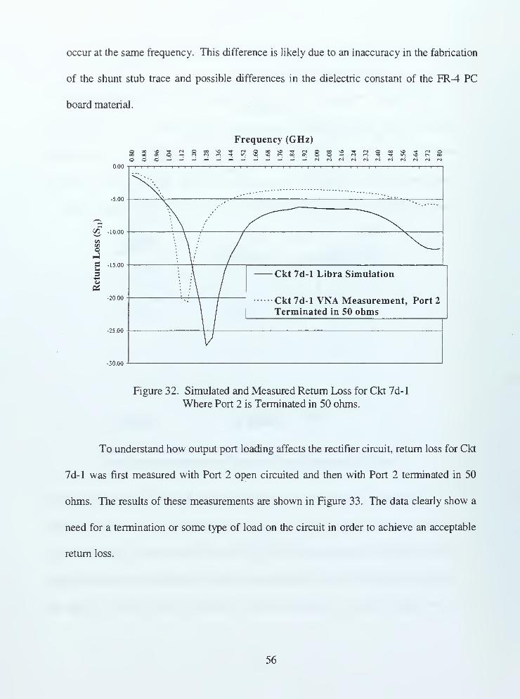
occur at the same frequency. This difference is likely due to an inaccuracy in the fabrication
of the shunt stub trace and possible differences in the dielectric constant of the FR-4 PC
board material.
Frequency (GHz)
o o c (N (N (N <N (N (N C4
0.00
-5.00
Cfl -10.00
cnoJC -15.00M3-M
-20.00
-25.00
-30.00
Ckt 7d-l Libra Simulation
Ckt 7d-l VNA Measurement, Port 2
Terminated in 50 ohms
Figure 32. Simulated and Measured Return Loss for Ckt 7d-l
Where Port 2 is Terminated in 50 ohms.
To understand how output port loading affects the rectifier circuit, return loss for Ckt
7d-l was first measured with Port 2 open circuited and then with Port 2 terminated in 50
ohms. The results of these measurements are shown in Figure 33. The data clearly show a
need for a termination or some type of load on the circuit in order to achieve an acceptable
return loss.
56

Frequency (GHz)
OeN^t'vOOOOCNTfsDOOOfN'^-vOOOOCJ
c/3
o-es-
3"5
OS
aou3
-5
-10
-15
-20
-25
i i i r~i ill! i r~i ! i" :-1
1 !
'
•Oct 7d-l, Port 2 Open
Ckt 7d- 1, Port 2 Terminated
Figure 33. VNA Measured Return Loss for 1.3 GHz Rectifier Circuit (Ckt 7d-l)
Without DC Motor Attached, Port 2 Configured with an Open Circuit
and with 50 ohm Termination.
A second version of the 1.3 GHz rectifier circuit was fabricated and assembled with
a miniature DC motor as a load on Port 2 (Ckt 7d-5). Figure 34 displays the return loss
measurements for the two conditions of Port 2: (a) connected to a miniature DC motor and
(b) terminated in 50 ohms. Comparison of data for the motor loaded rectifier shows that the
motor on Port 2 provides a better return loss than when Port 2 is terminated in 50 ohms.
Thus the rectifier circuit terminated with the motor seems to provide a better means to match
the input of the rectifier than when a 50 ohm termination is placed on Port 2.
57

Frequency (GHz)
OCN'^-'OOOOCNtI-^OOOOCN'^-vOOOOCNo o OJ CS CN CS CS (N CS
O_su3
-s
0.00
-2.00
-4.00
-6.00
-8.00
a -lo.oo
-12.00
-14.00
i i i i i I I I i I : I ! i ! i : i i i i i I i -i—i—i—l—i—
r
Ckt 7d-5, Port 2 Terminated with DC Motor
Ckt 7d-5, Port 2 Terminated in 50 ohms
Figure 34. VNA Measured Return Loss for 1.3 GHz Rectifier (Ckt 7d-5)
Port 2 Terminated with DC Motor and in 50 ohms.
G RECTIFIER CIRCUIT DESIGN - CONCLUSIONS
This chapter dealt with the design of the microstrip rectifier with a primary goal to
provide an impedance match to a 50 ohm coaxial transmission line input from the MAV
antenna. Further design to improve rectification efficiency is explored in Chapter V, where
rectification efficiency measurements are described. However overall efficiency is affected
by how much energy is passed through the rectifier rather than reflected from it. Therefore
providing a good impedance match from the antenna to the rectifier becomes important.
Design of the microstrip circuit required an accurate knowledge of the electrical
properties of the material being used. Properties such as dielectric constant of the substrate
and conductivity of the conductors influence the design of the microwave circuitry. Use of
58
the FR-4 PC board material was a serious impediment towards developing a good design
and maintaining circuit fabrications with low return loss. The relative permittivity of the
dielectric substrate was estimated from measurements on sample circuits that were
compared to the computer (Libra®) simulation results. However, it is shown that an error in
using an £rof 4.8 verses may have resulted in a 37 percent error for the relative dielectric
constant used in designing the microstrip circuit. This error resulted in the microstrip width
that was approximately 32 mils thinner (111 mils verses 147 mils) than should an £rof 3.5
had been used in the design calculations. This error also effects the determination of the
scattering parameters for the SMT-SBD package, thereby compounding the problem.
One major improvement in the design of this circuit would be to use a high quality
substrate. Use of a substrate with tightly regulated substrate parameters would provide
allow a more accurate design of the impedance matching circuit for the SMT-SBD package.
An example of a tightly controlled permittivity would be RO4350 high frequency woven
glass reinforced ceramic filled laminate, produced by Rogers Corporation of Chandler,
Arizona, USA. The RO4350 material has er=3.48 ±0.05 and can be fabricated into
microstrip circuits using the same etching or routing methods used on FR-4 PC Board
material.
Another improvement may be to use a high quality substrate with a high
permittivity. High quality substrates with a high permittivity would shrink the size of the
microstrip rectifier circuit, thereby providing an easier fit within the MAV structure. A
substrate material with high permittivity is RT/duroid 6010LM ceramic filled laminate also
produced by Rogers Corporation. RT/duroid 6010LM has er=10.2 ±0.25 . However,
59

fabrication methods for RT/duroid 6010LM are more complex as the substrate is ceramic
and typical FR-4 PC board etching methods are not reliable. Another high permittivity
substrate material is Epsilam-10 produced by the Electronic Products Division of the 3M
Corporation. Epsilam-10 has er=10.2 ±0.25 and uses a ceramic filled Teflon compound
for the substrate and can be processed like conventional printed circuit board material (such
as FR-4).
A second area of concern for rectifier circuit design is how to handle loading of the
rectifier. It is evident that the rectifier circuit must be loaded in order to avoid large return
losses. As shown in Figure 34, this load could be the miniature DC motor of the MAV.
However, the impedance discontinuity between the leads of the DC motor and the output
microstrip structure of the rectifier circuit increases the return loss, as shown in the
differences between Figure 33 and Figure 34. VNA measurements of return loss were
unstable when there was appreciable DC motor lead length. Minimization of these lead
lengths was determined to be essential in order to achieve repeatable results.
60

III. ANTENNA DESIGN
Previous researchers in wireless power transfer concentrated on developing antenna
systems that provided the greatest RF-to-DC conversion efficiency and could transfer large
amounts of power. Size and weight did not play a crucial role in determining antenna type
and usually these designs tended to be large flat array antennas. These antennas were
fastened to the bottom of the vehicle and provided WPT for a single orientation between the
transmitter and receiver. These configurations were acceptable for a stationary vehicle or
for a system that could retain a certain relative position and orientation between transmitting
and receiving antenna.
The operation of this vehicle (MAV) requires that wireless power transfer be
independent of rotation or position. Therefore the MAV receiving antenna must be able to
receive power from nearly any direction. In addition the antenna must not add appreciably
to the size nor to the weight of the vehicle. The receiving antenna must be an efficient
receiver of microwave energy and be able to transfer this energy to the rectifying circuit
with minimal signal loss or reflection.
This chapter describes the design and fabrication of the second basic part of the
MAV WPT receiving system: the antenna. This antenna must meet the operational
requirements described previously and fit within the physical parameters of the Lutronix
vehicle: a cylinder with diameter of 4.4 cm and length of 10.2 cm. This chapter describes
the antenna configuration, computer modeling and simulations conducted for antenna
design, fabrication of the antenna, and measurements.
61

A. ANTENNA TYPE SELECTION
One MAV requirement is to make the vehicle as lightweight as possible. With this
in mind, the vehicle body was chosen to become the antenna for WPT. Therefore, the MAV
body serves two purposes, as an antenna for wireless power transfer and as the physical
structure and aerodynamic shape for the MAV.
Two antenna types that could be chosen to meet the physical shape of the Lutronix
MAV are the conformal array antenna and the fat dipole antenna. A conformal array
antenna would require a complex feeding structure to interface the array to the rectifier.
This structure would add weight and require space on the vehicle.
The fat dipole antenna readily conforms to the size and shape of the Lutronix 's
MAV which is shown in Figure 35. A single coaxial feed can be used to minimize weight
and space requirements. The MAV's dimensional constraints required the dipole to be
approximately 10.2 cm in length and 4.4 cm in diameter. Design parameters not
constrained by the vehicle geometry include the feedpoint location, and size of gap about the
feedpoint.
10.2 cm
Figure 35. Dimensions for MAV Dipole Antenna.
62

B. DIPOLE ANTENNA GEOMETRY
Antenna design principally involved selecting the following parameters of the dipole
antenna: (1) overall physical length, (2) feed point location, and (3) feedpoint gap size. The
antenna design should maximize received power and provide a driving point impedance that
matches that of the interface to the rectifier circuit. This interface is a 50 ohm semi-rigid
coaxial cable which is used as the feed. The rigid coaxial cable also provides the
mechanical structure holding the microstrip rectifier circuit within the upper section of the
MAV antenna.
The maximum overall antenna length was determined by the size of the Lutronix
vehicle, however, it is worthwhile to understand how length affects the impedance
characteristics of the MAV antenna. MAV requirements coupled with technology
improvements will likely drive future MAVs towards a smaller size. Should a smaller
vehicle be considered, the impedance characteristics of the smaller antenna may require a
new operating frequency for WPT or changing system impedance to match the new driving
point impedance.
The radiation resistance is largely dependent upon overall length. Dipole antenna
radiation resistance for a thin dipole has been shown to be frequency dependent and can be
calculated by [Ref 14]
Rrad =^-{C + \n(kl)-Ci(kl) + ±-sm(kl)
in 2
x [Si(2H)-2S
i(H)]+-cos(M) (22)
x[C + \n(kl 1 2) + Ct(2kl) - 2C, (kl) ] }
63

where 77 is the free space impedance (377 ohms), / is the overall length of the dipole, k is
the free space wave number which is written as
Ink=—, (23)
and A is the wavelength in free space. The sine integral, S, (kl), and cosine integral, Ct(kl),
are defined as
S,M='^dy (24)
y
C,W =f^<fy . (25)
y
Figure 36 provides a plot of calculated radiation resistance vs. dipole length in terms
of wavelength for a thin dipole. Calculated radiation resistance verses thin dipole antenna
sizes for frequencies of interest (1.0 GHz, 1.3 GHz, and 2.45 GHz) are shown in Figure 37.
These plots demonstrate that higher transmit frequencies tend to increase the radiation
resistance for an antenna size on the order of the Lutronix MAV (10.2 cm in length).
Figure 37 also shows that a 10.2 cm long, thin dipole antenna would have a theoretical
radiation resistance close to 25 ohms at 1.0 GHz, 200 ohms at 2.45 GHz, and at 1.3 GHz the
radiation resistance is approximately 50 ohms, which is desired for impedance matching to
the rectifier circuit.
64

oc
GO
co
350
300
250
200
150
100
n 50
1 2
Dipole Length (wavelengths)
Figure 36. Dipole Antenna Radiation Resistance.
^ 250c«
E.co 200<uoGS3 150V)
• »<on
100
co
50-oc3
C* n
f= 1.0GHz
f= 1.3GHz
f= 2.45GHz
Dipole Length (cm)
Figure 37. Calculated Radiation Resistance for a Thin Wire Dipole
Antenna at Proposed WPT Frequencies.
65

The radiation resistances shown in Figure 36 and Figure 37 are based on a sinusoidal
current distribution over a thin wire dipole. A thick dipole may be expected to differ
significantly in radiation resistance and to have a significant reactance. Collin provides
radiation resistance and input reactance graphs for dipole antennas of varying wire thickness
[Ref 15]. Data for these graphs come from hundreds of impedance measurements made by
Brown and Woodward [Ref 16]. For thicker dipole antennas, the radiation resistance and
input reactance tend to have smaller variations over a wide range of frequencies. Selected
data points for a dipole antenna of length similar to the proposed MAV (10.2 cm) is shown
in Figure 38 for resistance and Figure 39 for reactance over the various frequencies of
interest (1.0 GHz, 1.3 GHz and 2.45 GHz).
66

PA
ac
1600
1400
1200
1000
800
600
400
200
— -X- f= 1.3 GHz
- ». - f= 2.45 GHzA
*
*
//
/
¥-i
$"i
$oC\J
ooDipole Length/Thickness
oo<3-
Figure 38. Radiation Resistance of 10.2 cm long Dipole Antenna
as Thickness Varies [Ref 15].
800
600
400
200
-200
-400
-600
a f i nrrn-r
,A --X--f=1.3GHz
- - a - -f= 2.45 GHz*
•
•
*
* * * m ** • *
o oo oo
Dipole Length/Thickness
Figure 39. Reactance for a 10.2 cm long Dipole Antenna
as Thickness Varies [Ref 15].
67

The fat dipole MAV antenna can be assumed to have complex impedance, similar to
that shown by Collin and not readily obtainable through analytical expressions. However
several numerical simulation methods exist to estimate the complex impedance of any
radiating structure. Use of numerical simulation methods allows the variation of multiple
antenna design parameters such as diameter, feedpoint position and feedgap size. By
varying one parameter while keeping others constant, impedance trends can be established.
One numerical method is called the Method of Moments (MoM), which was applied
to electromagnetics by Harrington [Ref 17]. MoM was used in computer simulations to
develop impedance trends for the MAV antenna while varying geometry parameters.
Numerical electromagnetic modeling for MoM calculations is discussed in Section C.
Results of computer simulations using a commercially available MoM computer code
(GNEC®) is discussed in Section D. MoM numerical simulations using GNEC® were
conducted to design an antenna feedpoint geometry that would have an impedance match to
the 50 ohm rigid coax cable feeding the antenna.
68

C. NUMERICAL ELECTROMAGNETIC CODE (NEC) MODELINGOFMAV ANTENNA (FAT DIPOLE ANTENNA)
Computer modeling and simulation of the fat dipole MAV antenna used an
adaptation of the Numerical Electromagnetic Code Version 4.1 (NEC 4.1) called
Government NEC (GNEC®). GNEC® is a Microsoft Windows 95/NT compatible computer
program produced by Nittany Scientific of Hollister, California [Ref 19]. GNEC® performs
electromagnetic calculations by using a modified form of NEC 4. 1 FORTRAN computer
program which is owned by the US Government and developed at the Lawrence Livermore
National Laboratory [Ref 19]. NEC 4.1 and GNEC® are US Government controlled
computer codes and have distribution limitations. Other less accurate versions of NEC
(NEC 2 and NEC 3) are available for export to other countries and are used world-wide.
The output of the NEC codes includes the antenna radiation pattern and current
distribution on the antenna structure at a single frequency. Antenna input impedance and
voltage standing wave ratio (VSWR) can be computed over a range of frequencies. The
NEC computer codes rely on text based input and output files. There are no tools for
visualization of the input geometry or the output data. GNEC®, however, provides a
graphical user interface (GUI) to NEC and allows visualization of input geometry files and
output data files in graphical form. Graphical output includes displays of wire frame
models, and at a single frequency, current distributions on the wires of the structure and
radiation patterns in both two-dimensional sections and three-dimensional volumetric plots.
Graphs of input impedance and VSWR over a frequency range can also be produced readily
by GNEC®.
69

The computational methods used for NEC and MoM codes require some knowledge
of how they operate in order to develop models that achieve accurate simulation results.
The following sections briefly describe the theory behind MoM type codes, (in particular
NEC 4.1 and GNEC®), discuss the antenna modeling requirements of these programs, and,
provide a description of how the MAV antenna GNEC® model was developed.
1. NEC - Method of Moments Solution Description
The NEC computer programs analyze the electromagnetic response of antennas and
scatters by a numerical solution of an integral equation using the Method of Moments
(MoM) described by Harrington [Ref 17]. Thin wire segments model antenna structures,
where inter-connected wire mesh grids approximate solid surfaces. When the structure is a
closed volumetric surface, then surface patches can be used to model the geometry. The
electric field integral equation (EFTE) is solved for wire frame models and the magnetic field
integral equation (MFTE) is solved when patches are used. A hybrid EFE-MFIE is solved
when both wires and patches are used.
The integral equations (IE) reduce to a set of linear simultaneous equations that are
solved using matrix methods. The first step is to assume a basis function for the current on
individual thin wire segments. MoM computer codes have used many different types of
basis functions for the current on a segment, however the most popular are the pulse and
sinusoidal functions. To calculate the current on the wire segment j , GNEC and NEC 4.1
use the three term sinusoidal expansion basis function,
Ij(s) = Aj + Bj sin k
s(s - Sj ) +C
;[cos ks {s -Sj ) -1] (26)
70

where s is the location on the wire segment for the current to be calculated, s * is the center
location of the wire segment, ks
is the wave number in the medium containing the wire, and
Aj , Bj , Cj are constants.
The three constants [Aj , Bj , Cj ) in (26) are solved for by applying the boundary
conditions at the ends of wire segments and on the surface of the wires. The boundary
conditions at the ends of wire segments require conformity to Kirchoffs Current Law
(conservation of current between segments). At the wire surface, Gauss' Law must be
satisfied where the tangential electric field is zero at the surface of a perfect electrical
conductor. Solutions for the three constants of the current basis function provide the
current on a single segment. The currents on all segments are solved for simultaneously by
GNEC® and NEC 4.1 using linear algebra techniques.
The NEC and MoM computer simulations start with a segmented wire frame model
of the structure (antenna) and a voltage specified at the feedpoint of the antenna. Values for
charges on wire segments and currents between wire segments of the model are then
computed. Circumferential variation of charge over each wire segment is neglected by
assuming the wire diameter to be thin (such as a filament). Thus current is only directed
along the wire axis and the circumferential component is zero. The voltage and computed
current at the feedpoint segment determine the complex driving point impedance or input
impedance of the MAV antenna.
Individual wires of the surface model are broken into smaller segments. The entire
model consists of segments of wires, some of which are connected to their nearest neighbor
on the same wire, and others connected to the segments of other wires. The proper selection
71

of length, thickness and interconnection between wire segments determines whether the
solution is converged and the simulation produces accurate results.
2. Modeling Rules
Wire frame models for NEC modeling of a structure must be developed with care in
order to provide accurate simulations. Parameters that are important and can vary with
frequency are wire segment length and diameter. Also important are how wire segments are
interconnected and the spacing of meshed wire segments when modeling a surface area.
The following paragraphs provide information on how these rules are determined. Table 5
provides a summary of these modeling rules for GNEC®.
a. Wire Segment Length (A)
GNEC provides greater accuracy as shorter and more numerous thin wire
segments are used to model the structure. However, complexity and computation time
greatly increase with the number of segments, and therefore, guidelines have been
developed that provide solution convergence with the minimum number of segments. The
fundamental guideline for wire segment length is that
A < 0.U , (27)
where X is the wavelength of the simulated electromagnetic source. When impedance
information is required or when modeling critical areas of the antenna, a shorter wire
segment used is used to increase the rate of solution convergence
A < 0.05/1 . (28)
Shorter segment lengths may not produce greater accuracy if the length to radius ratio
becomes too small. Therefore, lengths should not be any shorter than 2.5 times the wire
72

radius (a) in order for the segment to be considered a thin wire with negligible
circumferential current variation.
b. Wire Segment Radius (a)
Wire segment radius (a) selection is dependent upon three factors: (1) thin
wire approximation, (2) segment length to radius ratio — , and (3) the equal area rule for
modeling surface area. Circumferential variation of charge over each segment is neglected
by assuming that the wire radius is thin relative to wavelength of the electromagnetic signal
and much smaller than the segment length. A guideline provided by Burke [Ref 19] for
wire segment radius is
2# a. , ,„.—-«1 . (29)A
As noted earlier, segment lengths should be greater than 2.5 times the wire
radius to neglect the circumferential variation of currents on the wire segment. Therefore
the guideline for segment length to radius ratio is
- > 2.5 . (30)a
The equal area rule for wire segment radius is used when wires are
representing a solid surface area. A surface area is modeled with a wire mesh where
segment radius and length are chosen such that the wire surface area equals the area to be
represented by the wire or equivalently,
n
Area =^^ ina
i. (31)
f=l
73

Since many of the wires in a mesh model will typically represent a metal
surface area, the choice of segment radius requires careful consideration of neighboring
wires and geometry of the structure. Some mesh formations use converging wires such as
spokes in a wheel arrangement. When wires do converge, a tapered wire segment can be
used to achieve a better model. Burke [Ref 19] suggests a mesh size smaller than 0.1 A. on a
side with wire separation of at least 3 times the wire diameter.
c. Interconnection between Surface Mesh Wires
The GNEC® program will recognize that wires are connected only when the
segment ends coincide. If segment ends do not coincide within 0.001 times the shortest
segment length, then GNEC® will compute currents on the wire segments as though they are
not connected. Therefore, one must use caution to ensure that segments in the wire mesh
align at the wire segment ends.
Model Rule Parameter Guideline Comment
1 Segment Length (A) 2.5a < A < 0.05/1 Longer lengths reduce computation
time
2 Segment Radius (a) O.Ua <
In
GNEC® uses an approximation that
neglects circumferential currents on
wire segments. This assumption
becomes invalid for larger radius.
3a
3b
Surface Area
Modeling
n
Area =/
7raiA
i
Mor
2n a = d
First equation is most accurate,
however, the second equation has
proven to be sufficient for surface
areas away from discontinuities.
4 Wire Grid Spacing 6a<d<0.lA Grid spacing should be tighter near
antenna feed and discontinuities
5 Wire
Interconnections
Segment Ends must
coincide within 0.001AWhen possible identical coordinates
for endpoints should be used.
Table 5. GNEC® Model Parameter Guidelines.
74

3. MAV Antenna GNEC® Input Data File Development
GNEC® input data files describing the geometry of proposed MAV antennas were
developed using the guidelines previously described. Table 6 lists the range of values for
segment length and radius to meet the NEC modeling requirements listed in Table 5. Table
6 values assume a 1.3 GHz as the source operating frequency, which requires tighter
modeling specifications than the 1.0 GHz signal.
Geometry Variable Value Model Rule
(from Table 5)
Grid Spacing d <11 mm 4
Segment Length A <11 mm 1
Segment Radius
for Surface Modeling
(equal area rule)
a =1.1 mm for d = 1 1 mm 3b
Segment Radius
for Non-Surface Modelinga < 1.7 mm 2
Table 6. Acceptable Ranges for GNEC®/NEC 4.1 MAV Geometry Definitions.
A baseline GNEC® model of the MAV antenna was generated and then adjustments
were made to the position and size of the feed gap to optimize VSWR. Since the model is
symmetrical about the vertical centerline, the model was sectioned into wedges which
allows for a simplified GNEC® file description. The GNEC® input file includes a statement
(GM card) to copy and rotate the defined section about the vertical centerline. A sample
wire frame model with the wedge section is shown in Figure 40. Each wedge of the
simplified GNEC® model consists of wires defined to meet the modeling ranges specified in
Table 6. Some wires are defined as straight lines and others as arcs. Table 7 lists the
model's segment length and radius for the wires in the wedge.
75
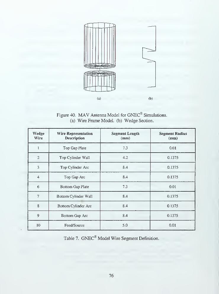
(a) (b)
Figure 40. MAV Antenna Model for GNEC® Simulations,
(a) Wire Frame Model, (b) Wedge Section.
WedgeWire
Wire Representation
Description
Segment Length
(mm)Segment Radius
(mm)
1 Top Gap Plate 7.3 0.01
2 Top Cylinder Wall 4.2 0.1375
3 Top Cylinder Arc 8.4 0.1375
4 Top Gap Arc 8.4 0.1375
6 Bottom Gap Plate 7.3 0.01
7 Bottom Cylinder Wall 8.4 0.1375
8 Bottom Cylinder Arc 8.4 0.1375
9 Bottom Gap Arc 8.4 0.1375
10 Feed/Source 5.0 0.01
,<BTable 7. GNEC Model Wire Segment Definition.
76

4. GNEC® Model Convergence
GNEC® impedance calculations were conducted using a single MAV antenna
geometry to determine impedance solution convergence of the GNEC® model. These
calculations were conducted to verify that sufficient detail was present in the GEC® model
to produce a stable impedance solution. The MAV antenna geometry used had a feed gap of
1.5 cm located at 42 percent from the lower end of the antenna.
Several GNEC models were produced for this antenna geometry with the level of
detail adjusted and the calculated impedance observed. If the calculated impedance change
between models with increasing levels of detail was small (less than 5 percent), then the
level of detail in the model was considered sufficient. Two principal areas of detail for the
MAV antenna model are discussed, (1): the applied voltage source area modeling, and (2):
circumferential wires for upper and lower surface sections.
a. Applied Voltage Source Area Modeling
According to Burke [Ref 18 and 19], the most critical area of the GNEC®
antenna model is the modeling of the voltage source, which means the positioning and
modeling of the immediate area around the source for the antenna. The GNEC
modeling source used was an applied voltage source located at the midpoint of the wire
joining the upper and lower sections of the MAV antenna (wire 10 of Table 7). Because
a three term basis function (26) is used in the current solution, a minimum of three wire
segments are required to be adjacent, in line, and without additional wire junctions. As
displayed in Figure 41, the calculated impedance for this wire using 3, 5, and 9 segments
has almost negligible change (less than 2 percent). Since calculated impedance changed
little for increased number of segments, GNEC® models can use a 3 segment wire
77


between the upper and lower sections with the voltage source applied to the center
segments and obtain impedance solution convergence at 1.0 and 1.3 GHz.
160.0
140.0
120.0
100.0
80.0
60.0
40.0
20.0
0.0
,^
>-•
M3 Segment Feed
5 Segment Feed
9 Segment Feedi i i ' ' ' ' i
i iooooooooooooooooooooooooooT-cMco-^-irjcDi^ooFrequency (MHz)
Figure 41. MAV Antenna Impedance for GNEC® Models with
3, 5 and 9 Segments for the Source Wire Model.
b. Circumferential Wires for Upper and Lower Surface Sections
GNEC® modeling requirements for a surface structure require a mesh grid
according to the rules presented in Table 5. A GNEC® model with a complete surface
mesh is shown in Figure 42. It was suspected that the circumferential wires on the upper
and lower surface sections may be removed from the model without effecting impedance
calculations if there is no current on them.. Removal of these circumferential wires
would greatly reduce the number of segments in the GNEC model thereby allowing
faster computation of antenna impedance. GNEC" models with and without
circumferential wires were developed. These models are shown in Figure 42 and Figure
43 with the currents superimposed. As shown, the circumferential currents are observed
in Figure 42 to be nearly zero. Also Figure 42 and Figure 43 show that the currents for
the simplified model with circumferential wires removed are roughly of the same
78


magnitude as that of the detailed model. A plot of the'GNEC® calculated input
impedance for the detailed and simplified models is shown in Figure 44. These results
demonstrate that the calculated impedance does not change much between these models.
Therefore, removal of the circumferential wires from the model can be done without
effecting the calculated antenna impedance solution.
As shown in Figure 42 and Figure 43, the model of the MAV antenna is
shown symmetric about a vertical centerline. Fabrication of a physical MAV antenna
with absolute symmetry about the vertical centerline is highly unlikely. An offset of the
source wire from the centerline will likely result in an increase in currents in the
circumferential direction. Therefore, some caution should be observed when interpreting
between the measured and calculated impedance for the MAV antenna.
79


®Figure 42. Currents for the Detailed GNEC model of a MAV Antenna
Current Log
-3200
-123.62
dfl
-215.25
®Figure 43. Currents for the Simplified GNEC Model of the MAV Antenna
80


160.0
140.0
sJ3©
a
120.0
100.0
80.0
o 60.0aE 40.0
20.0
0.0
^f^r^^
^^rrrrr^^^^4^^^^^ V\cAr\\\aA C*KWC* \hr\rueraiiea oiNtu mooci
ySSimplified GNEC Model
oo00
ooen
ooooo oo
CM
ooCO
ooNT
ooin
o o oo o oCD h- 00
Frequency (MHz)
Figure 44. The Calculated Impedance ofMAV Antenna
for Detailed and Simplified GNEC® Models.
81


D. GNEC® SIMULATIONS TO DESIGN ANTENNA FEED
The objective of the GNEC® computer simulations was to obtain an antenna
configuration with a driving point impedance close to that of the 50 ohm transmission line.
Since the overall length, thickness and shape had to match the Lutronix vehicle, the
parameters that could be adjusted were the position of the feed and size of the gap between
upper and lower sections of the dipole antenna.
GNEC" computer simulations of 58 separate antenna designs were conducted to
determine the best feed point positioning and gap size in order to provide an antenna with
close to a 50 ohm driving point impedance. These designs used the Lutronix MAV size and
then adjusted the feedpoint position from 50% from one end (i.e., center fed) to 10% from
one end. At each location, the feed gap was varied from 0.6 cm to 1.8 cm and input
impedance calculated.
Simulation results yield the complex input impedance of the MRPV antenna for the
two principal frequencies of interest (1.0 GHz and 1.3 GHz). Surface plots were made of
antenna input resistance, reactance and impedance as a function of feed location and feed
gap size. Figure 45 displays the GNEC® calculated resistance values, Figure 46 the
calculated reactance values and Figure 47 the GNEC® calculated impedance magnitude
values. Each figure has separate plots for the 1.0 GHz and 1.3 GHz test frequencies. Table
8 and Table 9 provide the reactance and impedance magnitude in tabular form. A 50 ohm
impedance is desired with minimum reactance, therefore an impedance tolerance of 45 to 55
ohms was selected and the smallest reactance determined. The optimum feed gap designs
are shown shaded in Table 8 and Table 9. The recommended antenna design is then
provided in Table 10.
82


70.0
60.0
50.0
MAV Antenna 40.0
Resistance
(ohms) 30.0
20.0
10.0
0.0
Feed Location from
60.0-70.0
50.0-60.0
40.0-50.0
30.0-40.0
20.0-30.0
10.0-20.0
0.0-10.0
Feed point
gap (cm)
(a) f= 1.0 GHz
70.0
60.0
50.0
MAV Antenna 40.0-
Re sistance
(ohms) 30.0
20.0
10.0
0.0
Feed Location from end (%)
60.0-70.0
50.0-60.0
40.0-50.0
30.0-40.0
20.0-30.0
10.0-20.0
0.0-10.0
1.8
Feed point
gap (cm)
(b) f= 1.3 GHz
Figure 45. MAV Antenna Resistance verses Feed Gap Size and Location
Computed using GNEC®. (a) 1.0 GHz. (b) 1.3 GHz.
83


MAV Antenna
Reactance
(ohms)
60.0-70.0
50.0-60.0
40.0-50.0
30.0-40.0
20.0-30.0
10.0-20.0
D 0.0-10.0
-10.0-0.0
-20.0--10.0
Feed Location from end (%)gap (cm)
(a) f=1.0GHz
MAV Antenna
Reactance
(ohms)
Feed Location from
58.0-68.0
48.0-58.0
38.0-48.0
28.0-38.0
18.0-28.0
8.0-18.0
-2.0-8.0
-12.0--2.0
Feed point
gap (cm)
(b) f=1.3GHz
Figure 46. MAV Antenna Reactance verses Feed Gap Size and Location•,®
Computed using GNEC . (a) 1.0 GHz. (b) 1.3 GHz.
84


MAV Antenna
Impedance
(ohms)
90.0-100.0
80.0-90.0
70.0-80.0
60.0-70.0
50.0-60.0
40.0-50.0
30.0-40.0
20.0-30.0
10.0-20.0
0.0-10.0
Feed Location from end (%)
Feed point
gap (cm)
(a) f= 1.0 GHz
MAV Antenna
Impedance
(ohms)
90.0-100.0
80.0-90.0
70.0-80.0
60.0-70.0
H 50.0-60.0
40.0-50.0
30.0-40.0
20.0-30.0
10.0-20.0
0.0-10.0
Feed Location from end (%)
1.8
Feed point
gap (cm)
(b) f= 1.3 GHz
Figure 47. MAV Antenna Impedance verses Feed Gap Size and Location
Computed using GNEC®. (a) 1.0 GHz. (b) 1.3 GHz.
85


1.0 GHz Input Reactance (ohms)
Gap
Position (%)
Gap Size (cm)
0.6 0.8 1.0 1.2 1.4 1.6 1.8
10 -16.9 -15.5 -12.7 -8.3 -4.5 0.1 4.1
20 -8.3 -4.1 0.8 6.4 11.5 16.7 23.5
25 -5.9 -1.0 4.4 10.6 17.2 24.2 31.4
30 -3.9 1.1 7.3 14.0 21.0 283 35.8
35 -2.4 3.2 9.6 16.6 23.8 31.4 39.1
40 -1.3 4.5 11.2 18.4 25.8 333 41.4
42.7 -0.9 5.0 11.8 19.0 26.5 343 42.2
47.5 -0.5 5.5 12.4 19.7 27.3 35.1 43.1
50 -0.4 5.6 12.5 19.8 27.4 35.2 43.2
1.0 GHz
(a)
Impedance Magnitude (ohms)
Gap
Position (%)
Gap Size (cm)
0.6 0.8 1.0 1.2 1.4 1.6 1.8
10 21.5 22.9 24.1 25.3 27.5 30.6 33.8
20 19.4 21.5 25.3 29.3 34.0 38.9 44.6
25 20.1 23.4 27.1 31.7 37.0 42.9 493
30 20.8 24.4 28.7 33.7 39.5 45.7 523
35 21.4 25.3 29.9 35.3 41.3 47.9 54.8
40 21.8 26.0 30.8 36.4 42.6 493 56.4
42.7 22.0 26.2 31.2 36.9 43.1 49.9 57.1
47.5 22.2 26.5 31.7 37.4 43.7 50.6 57.8
50 22.3 26.6 31.7 37.4 43.8 50.6 57.8
(b)
,®Table 8. GNEC Calculated Reactance and Impedance for 10.
Operating at 1.0 GHz. (a) Reactance, (b) Impedance
2 cm MAV Antenna
Magnitude.
86


1.3 GHz Input Reactance (ohms)
Gap
Position (%)
Gap Size (cm)
0.6 0.8 1.0 1.2 1.4 1.6 1.8
10 -2.2 0.4 3.9 9.1 13.9 19.4 24.6
20 0.9 5.0 10.0 16.1 21.9 28.1 36.2
25 1.1 5.6 11.4 18.3 26.1 34.7 43.9
30 1.4 6.4 13.1 20.9 29.6 39.2 49.4
35 1.9 7.6 14.9 23.5 33.1 43.4 54.4
40 2.3 8.5 16.4 25.7 35.9 46.8 58.5
42.7 2.5 8.8 17.1 26.6 37.0 48.2 60.0
47.5 2.6 9.2 17.6 27.3 38.0 49.4 61.4
50 2.6 9.2 17.7 27.4 38.1 49.5 61.6
(a)
1.3 GHz Impedance Magnitude (ohms)
Gap
Position (%)
Gap Size (cm)
0.6 0.8 1.0 1.2 1.4 1.6 1.8
10 9.0 11.6 15.4 20.3 25.6 31.8 37.9
20 14.5 20.1 26.1 33.2 40.6 48.4 57.5
25 17.7 24.3 31.0 38.9 47.7 57.2 67.4
30 20.7 27.5 35.5 44.3 53.9 64.2 75.2
35 23.1 30.9 39.4 48.9 59.1 70.1 81.7
40 24.9 33.2 42.3 52.3 63.0 74.4 86.4
42.7 25.6 34.1 43.5 53.6 64.5 76.0 88.2
47.5 26.3 35.0 44.6 54.9 65.9 77.6 89.9
50 26.3 35.1 44.7 55.0 66.1 77.8 90.1
(b)
^®Table 9. GNEC Calculated Reactance and Impedance for 10.
Operating at 1.3 GHz. (a) Reactance, (b) Impedance
2 cm MAV Antenna
Magnitude.
87
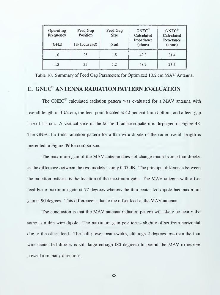
Operating
Frequency
(GHz)
Feed GapPosition
(% from end)
Feed GapSize
(cm)
GNEC®Calculated
Impedance
(ohms)
GNEC®Calculated
Reactance
(ohms)
1.0 25 1.8 49.3 31.4
1.3 35 1.2 48.9 23.5
Table 10. Summary of Feed Gap Parameters for Optimized 10.2 cm MAV Antenna.
E. GNEC® ANTENNA RADIATION PATTERN EVALUATION
The GNEC® calculated radiation pattern was evaluated for a MAV antenna with
overall length of 10.2 cm, the feed point located at 42 percent from bottom, and a feed gap
size of 1.5 cm. A vertical slice of the far field radiation pattern is displayed in Figure 48.
The GNEC far field radiation pattern for a thin wire dipole of the same overall length is
presented in Figure 49 for comparison.
The maximum gain of the MAV antenna does not change much from a thin dipole,
as the difference between the two models is only 0.05 dB. The principal difference between
the radiation patterns is the location of the maximum gain. The MAV antenna with offset
feed has a maximum gain at 77 degrees whereas the thin center fed dipole has maximum
gain at 90 degrees. This difference is due to the offset feed of the MAV antenna.
The conclusion is that the MAV antenna radiation pattern will likely be nearly the
same as a thin wire dipole. The maximum gain position is slightly offset from horizontal
due to the offset feed. The half-power beam-width, although 2 degrees less than the thin
wire center fed dipole, is still large enough (80 degrees) to permit the MAV to receive
power from many directions.
88

Ma* Gain (Front)
Ll_
jlMax)
Gain = 1 02 dB
- 3dB (Rigl
Ph.- 1U Leg
3 dB BeamWidth
- -'-:
Front/Back Ratio
90 270
180
Figure 48. GNEC Calculated Radiation Pattern for MAV-2 Antenna.
o
30
Wax Gnm (Fronf)
Gam = 2 08 dB
| Phi = 90 Dcr
Gain - 2 08 dB
Phi = 270 Peg
-ktB (Left ot Max)
Gain "1 08 dB
Phi = 131 Deg
-3dB(Riqh!otM«)
Gain = 1 08 dB
Phi - 41 Deg
3 dB BeemWidth
I82 Deg
Front/Bock. Ratio
o de
90
120
Figure 49. Radiation Pattern for a Thin Dipole of Same Length as MAV Antenna.
89


F. ANTENNA FABRICATION
This antenna was intended to only demonstrate remote power transmission, and as
such would be a non-flying model. Thus model weight was not considered a factor in the
choice of materials. An early fabrication attempt used copper foil wrapped about an
insulator. This technique proved unreliable and tended to leave conductive gaps along the
seams. An improved fabrication technique was devised by using 4.4 cm diameter copper
plumbing pipe cut to the desired length on a lathe. Copper endcaps were used as the center
feed gap area of the MAV dipole antenna. A slightly smaller diameter pipe section attached
the copper pipe (upper section of the antenna) to the upper endcap (upper feedgap). A thick
section of mylar was used to hold the upper and lower sections of the MAV antenna
together. Figure 50 displays a sample MAV antenna disassembled to illustrate the assembly
concept used.
Figure 50. Photographs of Copper Pipe MAV Antenna
Disassembled to Show Interior Connections.
90


This assembly allowed easy access to the interior of the antenna to install circuits. A
metal surface discontinuity existed on the upper antenna section between the copper endcap
serving as the upper feed gap and the copper pipe serving as the upper section of the
antenna. It was thought that this discontinuity would not appreciably effect the antenna's
electrical properties since it is very small and is likely to show little resistance at the
operating frequencies. The metal surface discontinuity could be eliminated by filling this
indentation with an electrically conductive paint or with solder, however, this was not done
since access to the interior circuitry was required for troubleshooting and evaluation.
The antenna feed consisted of a 50 ohm semi-rigid coaxial line that served to
connect the antenna to the rectifier circuit. The outer shield of the semi-rigid line was
soldered to the upper copper endcap and the center conductor was extended across the gap
and soldered to the lower copper endcap. The distance between these points is the feed gap
and is spanned by the center conductor and dielectric core of the semi-rigid coaxial cable.
The semi-rigid coaxial cable was fitted with a male SMA connector, prior to soldering to the
copper endcaps. The connector provided a convenient structural and electrical interface for
the microstrip rectifier circuit.
Assembly of the feed to the copper antenna required planning and prepositioning
techniques. Due to the rapid thermal transfer properties of a large copper area, the copper
endcaps required a great deal of heat to make an acceptable solder bond. Also applying the
rigid coaxial line when the heat was too great caused the interior dielectric of the semi-rigid
coax line to melt. Soldering the semi-rigid line to the endcaps required bringing the copper
endcaps up to temperature by the simultaneous application of several soldering irons until
solder would bond, then the rigid coaxial line was inserted though the drilled hole allowing
91


sufficient length to reach the opposite side of the feed. Solder was quickly applied on the
interior side of this connection electrically fusing the outer conductor to the upper feedgap
of the MAV antenna. The entire assembly was cooled immediately using de-ionized water.
The rigid coaxial line across the feed gap was stripped of the outer conductor and cut to the
length of the feed gap. The center conductor was attached to a connector pin, which was
soldered to the lower copper endcap. The connector pin provided a strain relief to prevent
the center conductor from breaking. These techniques were learned through trial and error.
Two antennas were fabricated, one each for the 1.0 GHz and 1.3 GHz operating
frequencies. Photographs of these two antennas are shown in Figure 51 with dimensions
annotated. The antennas were fabricated prior to completion of GNEC® simulations and
therefore did not use the GNEC recommended sizing for impedance matching. Rather, the
MAV antennas were fabricated using estimated dimensions obtained through VNA
measurements of VSWR while varying the feedgap between the upper and lower endcaps of
the antenna.
i
3 cm
9 cm
1
i
f
_3
i
3 cmr \
i
r
10.2 cm
(a) (b)
Figure 5 1 . MAV Antennas, Fabricated from 4.4 cm Diameter Copper Pipe,
(a) 1.0 GHz Version (MAV-1). (b) 1.3 GHz Version (MAV-2).
92


G. ANTENNA INPUT IMPEDANCE MEASUREMENT
The assembled MAV antennas were connected to the HP8510C Vector Network
Analyzer (VNA) as shown in Figure 52. A one port VNA calibration was conducted using
calibrated SMA loads. This calibration included the flexible coaxial cable interfacing the
VNA to the connector of the antenna. This calibration effectively subtracts out the effects of
the VNA and interfacing cabling so that the corrected measurement is very close to that of
the isolated device under test (DUT). Measurements of return loss, VSWR and input
impedance were made over the range 0.8 to 2.8 GHz for the two antennas fabricated. The
return loss for the two antennas is shown in Figure 53, VSWR in Figure 54 and input
impedance in Figure 55.
Figure 52. VNA Measurements on MAV Antenna.
93


REF 0.0 cB3 2.0 dB^V -6.6282 oB
log MAG
c
1PV or TTEFFP i i3C -1 LOKk 3 i. a og version
2 /
Ar12%*fy/
VVr*
V
MARKER i1.0 GHz-9.1743 dBl
PfMORKER 21.3 GHz-6.G282 dE
STORTSTOP
0.800000000 GHz2.800000000 GHz
28 JON 9E16:52:26
(a)
REF 0.0 dB
f2.0 oB-'-11.076 oB
log MAG
iov otJTEW* 1 10. 5 CM t jflMe 1.3 GH2 l ERST? tJ
V /
\J"w
WRKER i1.0 GHz-7.6782 oE|
ifMARKER 21.3 GHz-11.076 oE
STARTSTOP
0.800000000 GHz2.800000000 GHz
28 JON 8517:44:18
(b)
Figure 53. HP8510 VNA Measurement of Return Loss for MAV Antennas.
(a) 1.0 GHz Version; Length 13 cm (MAV-1).
(b) 1.3 GHz Version; Length 10.2 cm (MAV-2).
94


REF 1.02 2.0 -
V 2. Sill
SWR
Q
*RV fll TTENNf i i3C H LOW 5 i. GH2 VERSION
2r7
i: J\/ u
1.0 GHz2.1635
•fMPRKER 21.3 GHz2.6111
STARTSTOP
0.800000000 GHz2.800000000 GHz
28 J«N 9<
15:37:00
(a)
SiiREF 1.02 2.0 -
V 1.7603
SV«
r
«V ft TTE7FP i IB. = CM 1 .ONG i.S GH2 " 7&&TZ N
X—s
J~Ji;
\ r2
1.0 GHz2.5983
•fMPRKER 21.3 GHz1.7609
STORTSTOP
0.800000000 GHz2. 800000000 GHz
28 JAN 9317: 41: 04
(b)
Figure 54. HP85 10 VNA Measurement ofVSWR forMAV Antennas.
(a) 1.0 GHz Version, Length 13 cm (MAV-1).
(b) 1.3 GHz Version, Length 10.2 cm (MAV-2).
95

gll zREF 1.0 Units2 200.0 mUnits-'V 61.953 Q 58.674 nMftV ANTENMA 13CM U
(a)
Sn 2REF 1.0 Units2 200.0 mUnits/V 48.947 n -29.009 C5
MAV flNTENMA 10.2
WlHKtW i1.0 GHz36.58S n25.674 Q
»fMARKER 21.3 GHz61.953 n58.674 fj
28 JAN 9517:04:05
W=RkER i1.0 GHz114.92 rc
0.6357 n
•(MARKER 21.3 GHz48.947 Q
-29.008 fi
28 JON 9517:55:44
(b)
Figure 55. HP8510 VNA Measurement ofMAV Antenna Impedance,
(a) 1.0 GHz Version (MAV-1). (b) 1.3 GHz Version (MAV-2).
96

VNA measurements of the as-built MAV antennas show that the characteristics,
although not optimum, were sufficient for the WPT application. Both antennas exhibited a
return loss of close to 10 dB at their operating frequencies. The return loss and the VSWR
of these antennas were assumed to be sufficient to continue their use in developing the
wireless powered demonstrator models. Future work should investigate building MAV
antennas using the dimensions recommended in Table 10.
The VNA measurements of these antennas were affected by near field objects such
as hands and test equipment and therefore the results would sometimes vary. The data
shown in Figure 53 to Figure 55 were made with the MAV antenna situated on top of 4
inches of electromagnetic anechoic absorber foam. Measurements in this configuration
tended to be more consistent than when the antenna was situated directly on top of a metal
bench.
Figure 56 provides a comparison between the GNEC model of the MAV-2 antenna
and VNA measurements on the as-built antenna. The overall tread of VSWR shown in both
plots tends to increase as frequency increases, however the rate of increase displayed by the
GNEC results is much higher. It is likely that as the frequency increases, the GNEC model
used becomes less accurate and perhaps even incorrect. The reason for this claim is that the
GNEC model segment length has not decreased in relation to the increase in frequency. As
frequency increases above the values for which segment length and radius were developed,
the GNEC model diverges from the measured solution. The VNA measurements also
display much smaller values at the frequencies of interest than the GNEC calculations. The
as built MAV antenna contained a short length of 50 ohm rigid coaxial line that was not
included in the GNEC calculations and is not calibrated out in the VNA measurements. It
97

may be possible that this section of coaxial line may have helped provide a closer match to
50 ohms due to the reference plane shift introduced by the coaxial cable.
40.0
Frequency (MHz)
(a)
SllREF 1.02 2.0 -
V 1.7609
SVR
r
-«v ptrraw i IB. 5 CM 1 .ONG 1.3 gk? 7ERSTC N
X—y
JrUi:
\/*
s
M33KER i1.0 GHz2.5989
(fMORKER 21.3 GHz1.7S09
START 0.800000000 GHzSTOP 2.800000000 GHz
28 JON 9S17:41:04
(b)
Figure 56 Comparison ofVSWR Calculated by GNEC and that Measured by VNA for the
1.3 GHz MAV Antenna (MAV-2). (a) GNEC Calculation, (b) VNA Measurement.
98

H. ANTENNA DEVELOPMENT CONCLUSIONS
MAV antenna design using GNEC as a tool was useful, however some caution when
reviewing calculated results is required. Some parameters and effects on the MAV antenna
impedance can not be easily modeled in GNEC. These parameters include the actual feed
for the antenna, which is a semi-rigid coaxial cable, and the potential for an off center feed
wire to change the current patterns on the MAV structure. However the GNEC model does
provide an idea of how the feed gap location and size effects the impedance of the MAV
antenna.
Based upon the GNEC impedance calculations, a 10.2 cm long MAV antenna for
the 1.3 GHz operating frequency should have a 1.2 cm gap located 35 percent from the
bottom end. The as-built MAV antenna had a 1.5 cm gap located 42 percent from the
bottom. The GNEC impedance calculations indicated that the as-built antenna would have
impedance that is higher than the desired 50 ohms and the VNA measurements support this
result.
It is interesting to note how feed gap size effected the impedance of the antenna.
Consider the feed gap as a parallel plate capacitor with capacitance
C=^-eQ , (32)
a
where a is the radius of the antenna, d is the gap spacing and eQ is the free space
permittivity. Then from (32), one would expect the antenna reactance to become more
capacitive as the gap size is made smaller. Indeed as displayed in Figure 46, as gap size
decreases, the reactance decreases from positive values. This seems to indicate that the gap
99

100

IV. RECTIFIER CONVERISON EFFICIENCY MEASUREMENTS
A. INTRODUCTION
This chapter presents the rectifier RF-to-DC conversion efficiency testing that was
conducted on several microstrip rectifier designs and explains the techniques used to
measure rectifier conversion efficiency. Rectifier conversion efficiency has been the chief
measure of the performance of microwave rectification circuits. This conversion efficiency
has been defined many different ways by various researchers. Some of these conversion
efficiencies are more applicable to entire transmission system and include effects such as
transmitter losses and antenna efficiencies. This thesis is interested in maximizing the
efficiency of the rectifier circuitry and, in that regard, the efficiency measurements defined
for this work deal with the rectifier circuit only and disregard the loss contributions of the
transmitter, transmission path and antenna.
In this thesis, the rectifier conversion efficiency is defined as the ratio of average DC
power measured at the output of the microstrip rectifier circuit to the average incident
microwave power measured at the input to the microstrip rectifier circuit or
pPercent Efficiency = 100 , (33)
"rf
where PDC is the average DC power measured at the output of the microwave rectifier
circuit and PRF is the microwave power into the rectifier circuit. PRF is the difference
between incident and reflected microwave power measured at the input of the rectifier
circuit. Critical to the accuracy of this experiment are measurement of output DC power
(PDC ) , incident microwave power {Pincident ) , and reflected microwave power \Preflected )
101

Average DC power (PDC ) at the output of the rectifier was obtained using digital
multi-meter measurements of voltage across a lumped element load or voltage across and
current through a miniature DC motor load. The input microwave power values were
obtained by coupling a sample of incident microwave power via a directional coupler, and
measuring the sampled microwave power using a thermocouple sensor based microwave
power measurement system (specifically the Hewlett Packard HP438A dual channel power
meter with two HP8481A thermocouple power sensors).
Rectifier efficiency measurements were conducted using single frequency or
continuous wavelength (CW) and pulse modulated CW microwave signals. The CW and
pulse modulated CW signals were at 1.0 and 1.3 GHz. Pulse width and repetition rate (prf)
for pulse modulated CW signals were varied to determine effects upon rectification
efficiency.
Efficiency measurements were also made with several types of loads. These loads
included lumped element surface mount (chip) resistors, parallel resistive-capacitive (RC)
lumped element loads and miniature permanent magnet DC motors. It will be shown that
circuit loading influenced the efficiency of the rectifier circuit.
Section B of this chapter discusses how these measurements were made. Section C
presents the measurements in graphical form, while Section D provides a summary of the
results. Section E suggests some microwave rectifier improvements based on the results of
the efficiency measurements.
102

B. CONVERSION EFFICIENCY MEASUREMENT DESCRIPTION
A block diagram of a RF-to-DC conversion efficiency measurement apparatus for
single frequency or CW input signal with a resistive load is shown in Figure 57.
Microwave Signal
Source (HP8350Awith HP83592B Plugin)
MicrowaveAmplifier
(HP8347A)
Ch 1 Microwave Dual
Channel Power Meter
Ch2 (HP437A)
Multimeter
set to DC Volts
(HP3478A)
/ Power Sensor Heads(HP8481A) MAV Rectifier Circuit
with Chip Resistor Load
II> <-
Dual Directional
Coupler (Narda 3022)
Double Stub
Tuner ~v-5-
Figure 57. Block Diagram of RF-to-DC Conversion Efficiency Measurement
CW Input Signal and Chip Resistor Loading.
A thermocouple power sensor (HP8481A) connected to channel 1 of the digital
power meter (HP438A) measured the incident microwave CW signal at a frequency of 1.0
GHz or 1.3 GHz. Reflected microwave power from the MAV rectifier circuit was measured
on channel 2 of the power meter. An adjustable external double short circuit stub tuner is
used to impedance match the MAV rectifier circuit to the signal source circuit, which had a
characteristic impedance of 50 ohms. The tuner is adjusted by varying the length of two
parallel short circuits to achieve minimum reflected power as measured by channel 2 of the
power meter. DC output power from the rectifier circuit is obtained by measuring the
103
average voltage across the chip resistor load. Amplifier gain settings were varied to obtain
incident microwave power from mw to 180 mw.
When the input power was pulsed, as when simulating a radar transmitter as the
power source, or when the load is not a simple resistive load, the conversion efficiency
measurement apparatus was modified. Figure 58 shows the measurement setup for a pulsed
CW incident power signal and Figure 59 the measurement setup for a miniature DC motor
load using the pulsed CW incident power signal. The measurement apparatus used in
Figure 58 and Figure 59 provided incident average power levels up to 700 mw for CW
signals, which were much larger than the power levels for the test apparatus of Figure 57.
The measurement configurations in Figure 58 and Figure 59 have two differences:
(1) the loading of the MAV rectifier circuit, and (2) the manner in which the applied DC
power is measured. These configurations used a radar target simulator to build a pulse of
width (r) and repetition frequency (/ ) that was used to modulate the 1.0 GHz or 1.3 GHz
CW microwave signal. The Tektronix 477 analog oscilloscope provided a trigger pulse (B
gate trigger) that set the pulse repetition frequency (prf) which was displayed on the HP5248
electronic counter. The radar target simulator set the pulse width at 7 (is, similar to the
waveform of the transmitter of the AN/SPS-58 air search radar.
The pulsed output from the radar target simulator modulated the CW signal from the
HP8614A signal generator and was amplified by the HP489A microwave traveling wave
tube (TWT) amplifier. An isolator was used on the output of the TWT to protect the
amplifier from potential reflections of power from the test circuitry. A tiny sample, 30 dB
lower than the pulse modulated microwave signal, was coupled by the Narda 3002-30
104

directional coupler and detected using the HP432A detector. The envelope of the pulse-
modulated signal was displayed on the Tektronix 446 analog oscilloscope.
The incident and reflected microwave power was measured using the HP8481A
thermocouple power sensor heads and HP438A dual channel digital power meter. A
Tektronix 11801A high-speed digital sampling oscilloscope was used to observe the pulse
modulated CW microwave signal incident on the MAV microstrip rectifier circuit and the
rectified output of the MAV. The high-speed sampling oscilloscope provided insight to the
time domain characteristics of the rectifier output signal. DC power provided by the MAV
rectifier circuit was determined by measuring the average voltage across the chip resistor
load using a HP3578A digital multimeter. When the load was a miniature DC motor, the
resultant DC power was determined by measuring the current through and voltage across the
motor using two HP3478A multimeters as shown in Figure 59.
105

Microwave Signal Generator
(HP 8614A)RFOut
Electronic Digital
Counter (HP 5248)AC
RF ™ Modulator Mod In
(HP 8403A)
RFOut Sync Out
IRFIn
RFOut
MicrowaveTWT Amplifier
(HP 489A)
Pulse~ Radar Target Simulator
Trigger Input
Analog Oscilloscope
(Tek 2335)
Ch2 Ext Trigger
RF In Isolator
RF Out (Microwave Assoc 7M025)
Analog Oscilloscope
(Tek 466)
Ch 1 B Gate Trigger
Directional Coupler
(Narda 3002-30)
-30dB
Detector
(HP432A Neg)
I
-20dB
I
Bi-Directional Coupler
(Narda 3022)
-20dB
Chi
Ch2
Microwave
Dual Channel
Power Meter(HP 438A)
Power Sensor Heads(HP 8481 A)
-20dB
Directional Coupler
(Onmi-Spectra
4K15-001CHA)
lOdBAttenuator
Trigger High Speed Sampling
Input Oscilloscope (Tek 1 1801 A)
Sampling Head (SD-11)
Ch 1 Ch 2
Sampling Probe
!£
Sampling
Probe
+-*/ ~v
SMAto4mm adapter MAV Rectifier Circuit
with Chip Resistor Load
&Multimeter
DC Volts
(HP3478A)
\SNSMAto4mm adapter
Figure 58. Block Diagram of RF-to-DC Conversion Efficiency Measurement,
Pulsed CW Input Signal and Chip Resistor Loading.
106

Microwave Signal Generator
(HP 8614A)RFOut
Electronic Digital
Counter (HP 5248)AC
RF In Modulator Mod In
(HP 8403A)
RFOut Sync Out
IRFIn
RFOut
MicrowaveTWT Amplifier
(HP 489A)
Pulseq Radar Target Simulator
Trigger Input
Analog Oscilloscope
(Tek 2335)
Ch2 Ext Trigger
RF In Isolator
RF Out (Microwave Assoc 7M025)
Analog Oscilloscope
(Tek 466)
Chi B Gate Trigger
Directional Coupler
(Narda 3002-30)
-30dB
Detector
(HP432A Neg)
-20dB
t
Bi-Directional Coupler
(Narda 3022)
-20dB
Chi
Ch2
MicrowaveDual Channel
Power Meter(HP 438A)
1
1
Power Sensor Heads(HP 8481 A)
-20dB
Directional Coupler
(Onmi-Spectra
4K15-001CHA)
lOdBAttenuator
Trigger High Speed Sampling
Input Oscilloscope (Tek 1 1 80 1 A)
Sampling Head (SD-11)
Ch 1 Ch 2
Sampling Probe
^Sampling
Probe
*o*/SMAto
4mm adapter
~u
\\/Multimeter
DC amps
(HP3478A)
MAV Rectifier Circuit
with Chip Resistor Load
\s\SMAto4mm adapter
Mini
DC Motor
\
Multimeter
DC Volts
(HP3478A)
Figure 59. Block Diagram of RF-to-DC Conversion Efficiency Measurement,
Pulsed CW Input Signal and DC Motor Loading.
107

Microwave Signal Generator
(HP 8614A)RFOut
Electronic Digital
Counter (HP 5248)AC
RF m Modulator Mod In
(HP 8403A)
RFOut Sync Out
IRFIn
RFOut
Microwave
TWT Amplifier
(HP 489A)
Pulse~ Radar Target Simulator
Trigger Input
Analog Oscilloscope
(Tek 2335)
Ch2 Ext Trigger
RF In Isolator
RF Out (Microwave Assoc 7M025)
Analog Oscilloscope
(Tek 466)
Chi B Gate Trigger
Directional Coupler
(Narda 3002-30)
-30dB
Detector
(HP432A Neg)
I
-20dB
I
Bi-Directional Coupler
(Narda 3022)
-20dB
Chi
Ch2
Microwave
Dual Channel
Power Meter(HP 438A)
Power Sensor Heads(HP 8481 A)
-20dB
Directional Coupler
(Onmi-Spectra
4K15-001CHA)
lOdBAttenuator
Trigger High Speed Sampling
Input Oscilloscope (Tek 1 1801 A)
Sampling Head (SD-11)
Ch 1 Ch 2
Sampling Probe
ESampling
Probe
*[Z>>-/ T
SMAto4mm adapter MAV Rectifier Circuit
with Chip Resistor Load
VMultimeter
DC Volts
(HP3478A)
\SNSMAto4mm adapter
Figure 58. Block Diagram of RF-to-DC Conversion Efficiency Measurement,
Pulsed CW Input Signal and Chip Resistor Loading.
106

Microwave Signal Generator
(HP 8614A)RFOut
Electronic Digital
Counter (HP 5248)AC
RF In Modulator Mod In
(HP 8403A)
RFOut Sync Out
IRFIn
RFOut
MicrowaveTWT Amplifier
(HP 489A)
Pulse~ Radar Target Simulator
Trigger Input 4
Analog Oscilloscope
(Tek 2335)
Ch2 Ext Trigger
RF In Isolator
RF Out (Microwave Assoc 7M025)
Analog Oscilloscope
(Tek 466)
Chi B Gate Trigger
Directional Coupler
(Narda 3002-30)
-30dB
Detector
(HP432A Neg)
-20dB
t
Bi-Directional Coupler
(Narda 3022)
-20dB
Chi
Ch2
MicrowaveDual Channel
Power Meter(HP 438A)
Power Sensor Heads(HP 8481 A)
-20dB
Directional Coupler
(Onmi-Spectra
4K15-001CHA)
lOdBAttenuator
Trigger High Speed Sampling
Input Oscilloscope (Tek 1 1 80 1A)
Sampling Head (SD-11)
Ch 1 Ch 2
Sampling Probe
E/ ~V
SMA to
4mm adapter ^^^ Rectifier Circuit
with Chip Resistor Load
\s\SMA to
4mm adapter
Mini
DC Motor
I^T
51^ DC ampsV
1
?T0
)e
(HP3478A)
1 —H 1\
/ ST
Multimeter
DC Volts
(HP3478A)
Figure 59. Block Diagram of RF-to-DC Conversion Efficiency Measurement,
Pulsed CW Input Signal and DC Motor Loading.
107

1. Microwave Power Measurements
Measurement of incident and reflected microwave power ( Pincuient and Prejiecteci
)
were made using a dual microwave power meter (Hewlett Packard model 43 8A) and two
thermocouple based sensors (Hewlett Packard model 8481 A). Since the incident
microwave power measurement is crucial to accurate conversion efficiency calculation,
characterization of these power sensor devices is necessary in order to understand how their
use may effect the conversion efficiency measurement.
The HP8481A power sensor consists of two thermocouples connected in series.
Thermocouples are heat-based sensors and are considered to be true averaging microwave
power detectors. Each thermocouple consists of two dissimilar metals. They are joined
together in two junctions, one of which is heated by incident microwave energy and the
other is left at room temperature. These junctions, called the "hot" and "cold" junctions,
generate an emf due to two effects, one being the voltage due to dissimilar metals and the
second effect due to the heating of one junction causing electron diffusion and an opposing
electric field due to Coulomb's law. The combined effect, referred to as the Seebeck Effect
[Ref 201, provides a net thermoelectric DC voltage of the thermocouple junction.
The DC voltage generated by each thermocouple is very low. The specifications for
the HP8481A sensor give 160 nano-volts for every 1 micro-watt of incident microwave
power. Additional circuitry in the power sensor and meter are used to transmit the
thermocouple signal along a length of cabling to the power meter without effecting the
power measurement. Circuitry within the sensor chops the tiny measured DC voltage to
form a square wave. The square wave is amplified and AC coupled to the transmission line
leading to the power meter. The square wave signal is synchronously detected at the power
108

meter to produce the power measurement. Figure 60 provides a block diagram of the
Hewlett-Packard microwave power measurement system using thermocouple sensors.
RFInput
HP 8481APower Sensor
Thermocouple
Chopper
Amplifier
Cable
Zero
iHP 438A Power Meter
(Single Channel Shown)
Autozero Meter
Cal rg-Factor
~
220 HzMultivibrator
Range^Synchronous
Detector
AmplifierAmplifiers
and
Attenuators
50 MHzReference
Oscilllator
Figure 60. Block Diagram of Microwave Power Measurement System
using the Hewlett Packard HP8481A Thermocouple Sensor
and HP438A Power Meter [Ref 20].
Prior to making a power measurement, each thermocouple power sensor was first
zeroed at the power meter and then calibrated using a 50 MHz, 1 mW reference signal from
the power meter. The calibration was conducted whenever equipment was energized and
during every 4 hours of operation.
Although diode power sensor technology could have been used to measure
microwave power, available diode power sensors provide accurate square law values, and
hence linear power measurements, only at lower power levels (-70 dBm to -20 dBm).
109

Thermocouple power sensors, such as the HP 8481A sensor, ' maintain pure square law
power detection for higher power levels, from -30 dBm to +20 dBm. Newer wide dynamic
rage diode power sensors, such as the Hewlett Packard model E4412A, can provide CW
power measurements from -70 to +20 dBm. However, for modulated signals such as a
pulsed CW signal from the AN/SPS-58 radar transmitter, even these new diode power
sensors do not provide accurate square law detection.
2. Rectified Output Average Power Measurements
The measurement of average or DC power on the output side of the MAV rectifier
circuit was less straightforward than the incident power measurements. It was discovered
through experimental trials that the type of circuit load affected the rectifier efficiency
measurements. The actual loading for the MAV application would be either a battery system
or a miniature DC motor. Therefore two types of circuit loading were used for the MAV
rectifier efficiency measurements. The battery system loading was simulated in these
measurements by the use of a 37-ohm chip resistor load. An inexpensive miniature DC
permanent magnet hobby motor was used for the miniature DC motor loading case.
When the chip resistor loading was used, measurements of PDC were made by
measuring the average DC voltage across a chip resistor (37 ohm) load, as indicated in
Figure 57. This chip resistor was surface mounted to the microstrip rectifier board with one
side at the rectifier output voltage and the other soldered to ground using a via through the
microstrip board. A HP3478A digital multimeter was used to make the average voltage
measurement. High impedance probes were not available and therefore the multimeter test
leads may have loaded the rectifier circuit.
110

When the rectifier circuit was loaded by the miniature DC motor, PDC was
determined by measuring both voltage across and current through the permanent magnet DC
motor load. Measurements were made using two HP3478A digital multimeters, one each
for voltage and current. The multimeter measuring average or DC current was located
within the output circuit, it was not known whether or not the multimeter may have affected
the measurement.
Ill

C. CONVERSION EFFICIENCY MEASUREMENT RESULTS
Table 11 provides a listing of conversion efficiency measurements that were
conducted for several rectifier circuits with various loading conditions. Loading conditions
consisted of: (a) chip resistor; (b) chip resistor with external capacitor and (c) miniature DC
motor.
Figure Circuit
Designation
Description Input Signal Circuit
Loading
Figure 61 m3-2 Dual Si-SBD Rectifier,
external double shunt
stub impedance tuner.
1.0 GHz CW DC Motor;
Chip Resistor
Figure 62 m4-2 Dual Si-SBD Rectifier
external double shunt
stub impedance tuner.
1.0 GHz CW DC Motor
Figure 63 m7d-9 Single Si-SBD Rectifier
with Shunt Stub
impedance element
1.3 GHz CW;Pulsed 1.3 GHz CW
Chip Resistor;
Chip Resistor
plus capacitor
Figure 64 m8d-8 Dual Si-SBD Rectifier
with shut stub
impedance element
1.3 GHz CW;Pulsed 1.3 GHz CW
Chip Resistor;
Chip Resistor
plus capacitor
Figure 65 m8d-8 Dual Si-SBD Rectifier
with shut stub
impedance element
Pulsed 1.3 GHz CW Chip Resistor;
Chip Resistor
plus capacitor
Table 11. Summary of Rectifier Efficiency Measurements.
The maximum rectifier efficiency obtained was approximately 30% for the
configurations listed in Table 11. This efficiency is shown in Figure 61 and occurred for the
two parallel SBD circuit configuration at an input signal of 1.0 GHz CW with a miniature
DC motor as the load. This particular circuit configuration used an external double shunt
short circuit stub tuner to match the rectifier impedance to the 50 ohm line. The tuner was
112

adjusted to maximize power transfer at all input power levels which allowed the rectifier
circuit to be matched to the line at the power level tested. This reduced the input reflection
coefficient of the circuit, because the input impedance of Si-SBD changes with input power
level. Subsequent circuit designs, namely Circuit m7d-8 and m7d-9, incorporated a single
short circuit stub tuner located on the rectifier microstrip circuit. This microstrip element,
which does not allow impedance tuning for different input power levels, was necessary to fit
the entire MAV rectifier within the physical envelope of the MAV antenna.
Subsequent circuit designs (Circuit m7d-8, m7d-9) were not measured for average
power output using a DC motor loading since these designs incorporated a 37 ohm chip
resistor load into the MAV rectifier circuit. Measurement of voltage across a DC motor
alone can not describe the operating power level of the motor since the voltage across a DC
motor varies as
Vm =I.R*+K9 a, , (34)
where Va is the average voltage across the motor terminals, Ia is the current supplied to
the motor, R^ is the motor resistance at DC, Kv a constant that accounts for the magnetic
flux of the field and cor is the motor speed [Ref 21]. Measurement of both voltage across
and current through the DC motor is required in order to obtain the power supplied to the
motor. The available equipment to measure current, a multimeter, would be in series with
the DC motor load and the microwave signal loading effects of the multimeter were
unknown. Therefore it was decided to focus on measuring rectifier average output power
using the chip resistor loading where the output transmission lines could be kept short and
adverse effects minimized.
113


35.0
£25.0
20 40 60 80 100 120 140 160 180 200
Average Input Power Absorbed [Pinc-Pref] (mW)
Figure 61 . MAV Rectifier Efficiency Measurements for Two Parallel
Si-SBD Microstrip Rectifier Circuit (Circuit M3-2) with External
Double Short Circuit Stub Impedance Matching Tuner.
(a) 1.0 GHz CW Input Signal with Miniature DC Motor as Load.
(b) 1.0 GHz CW Input Signal with Miniature DC Motor as Load.
(c) 1.0 GHz CW Input Signal with 10 ohm Lumped Element Resistor as Load.
114


30.0
25.0
uB
E-u<u
iS
v
20.0
15.0
10.0
5.0
0.0
(b)
m4-2cw motor-
1
+ - m4-2cw motor-2
50 100 150 200
Average Input Power Absorbed [Pinc-Pref] (mW)
250
Figure 62. MAV Rectifier Efficiency Measurements for two Parallel
Si-SBD Microstrip Rectifier Circuit (Circuit m4-2) with External
Impedance Matching Tuner.
(a) 1.0 GHz CW Input Signal with Miniature DC Motor as Load.
(b) 1.0 GHz CW Input Signal with Miniature DC Motor as Load (Second Data Set).
115


25.0
200 400 600 800 1000
Average Input Power Absorbed [Pjnc-Prrf] (mW)
Figure 63. MAV Rectifier Efficiency Measurements (Circuit m7d-9)
Single Si-SBD Microstrip Rectifier Circuit
with Shunt Stub Impedance Matching.
Circuit Loading:
(Solid Line) 39.7 ohm Chip Resistor with 10 uF Capacitor in Parallel.
(Dashed Line) 39.7 ohm Chip Resistor.
Input Signals:
(a) 1.3 GHz CW.(b) 1.3 GHz CW Modulated by 7uS Pulse at prf= 36k (Duty Cycle= 0.25).
(c) 1.3 GHz CW Modulated by 7 uS Pulse at prf= 13k (Duty Cycle= 0.09).
(d) 1.3 GHz CW Modulated by 7 uS Pulse at prf= 3k (Duty Cycle= 0.02).
1200
116


30.0
— • •*• —
.
(a)
-* * » «
100 200 300 400 500 600
Average Input Power Absorbed [Pinc-Pref] (mW)
700 800
Figure 64. MAV Rectifier Efficiency Measurements (Circuit m7d-8)
Two Parallel Si-SBD Microstrip Rectifier Circuit
with Shunt Stub Impedance Matching.
Circuit Loading:
(Solid Line) 39.7 ohm Chip Resistor with 10 uF Capacitor in Parallel.
(Dashed Line) 39.7 ohm Chip Resistor.
Input Signals:
(a) 1.3 GHz CW.(b) 1.3 GHz CW Modulated by 7uS Pulse at prf= 36k (Duty Cycle= 0.25).
(c) 1.3 GHz CW Modulated by 7 uS Pulse at prf= 13k (Duty Cycle= 0.09).
(d) 1.3 GHz CW Modulated by 7 uS Pulse at prf= 3k (Duty Cycle= 0.02).
117

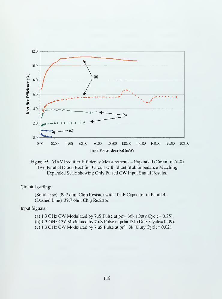
12.0
10.0
*
c'3
aua*
C
OS
0.0
0.00 20.00 40.00 60.00 80.00 100.00 120.00 140.00 160.00 180.00 200.00
Input Power Absorbed (mW)
Figure 65. MAV Rectifier Efficiency Measurements - Expanded (Circuit m7d-8)
Two Parallel Diode Rectifier Circuit with Shunt Stub Impedance Matching
Expanded Scale showing Only Pulsed CW Input Signal Results.
Circuit Loading:
(Solid Line) 39.7 ohm Chip Resistor with 10 uF Capacitor in Parallel.
(Dashed Line) 39.7 ohm Chip Resistor.
Input Signals:
(a) 1.3 GHz CW Modulated by 7uS Pulse at prf= 36k (Duty Cycle= 0.25).
(b) 1.3 GHz CW Modulated by 7 uS Pulse at prf= 13k (Duty Cycle= 0.09).
(c) 1.3 GHz CW Modulated by 7 uS Pulse at prf= 3k (Duty Cycle= 0.02).
118


D. SUMMARY OF CONVERSION EFFICIENCY RESULTS
Conversion efficiency measurements demonstrated the nonlinearly of Si-SBD
circuitry and that rectifier circuit loading can influence rectifier conversion efficiency.
Specifically the following effects were observed in the rectifier efficiency measurements.
1. Minimum Incident Power Requirement
A minimum input power level was required to achieve an average output or DC
power and therefore rectification. This minimum incident microwave power level was
larger when the load was a DC motor. This effect is seen clearly in Figure 61 for Circuit
m3-3 and Figure 62 for Circuit m4-2.
2. Applied Microwave Power for Peak Rectifier Efficiency
The efficiency peaked for incident microwave signal power after which the
efficiency either held constant or began to drop. Efficiency for the single Si-SBD
configuration peaked at 20 percent for approximately 100 mW of average microwave
power. Increasing the incident microwave power showed a noticeable drop in rectifier
efficiency as shown in Figure 63 for Circuit m7d-9. The peak for the two parallel Si-SBD
configuration also peaked at approximately 20 percent, however, this peak occurred at 200
mW of average microwave power. Rectifier efficiency was observed to hold constant at 20
percent for average microwave powers above 200 mW
3. Efficiency Decrease for Incident Power Above Peak Efficiency
When incident microwave power levels exceeded the level at which peak rectifier
efficiency was achieved, the rectification efficiency had the tendency to decrease as the
incident power level was increased. This effect is clearly shown in Figure 63 for the single
119

SBD diode circuit, m7d-9. As the power level increases, the current through the diode
increases and corresponding ohmic or I2R losses increase. These ohmic losses across the
diode generate heating which, if increased too high, can result in destruction of the Si-SBD.
Device heating from the increased ohmic losses can also increase the diode impedance and
result in larger reflected microwave power \Preflected) > which further erodes the rectifier
efficiency.
4. Multiple SBDs in Parallel Increase the Rectifier's Power Rating
When multiple SBDs in parallel were used, the peak rectifier efficiency remained at
peak performance values for a wider range and larger incident microwave power levels than
when the circuit contained only a single SBD. This result is clear from the data graphed in
Figure 65 for the two parallel Si-SBD rectifier circuit, m7d-8. Incident microwave power
values for peak efficiency increased slightly, but was not too appreciable. Therefore by
using multiple SBD in a parallel arrangement, a rectifier circuit can be produced that would
rectify higher incident power levels with no decrease in efficiency and does not require a
much larger incident power to operate.
5. Circuit Loading Affects the Rectifier Efficiency
When a parallel capacitance was added to the chip resistor load, the rectifier
conversion efficiency was noticeably increased. Figure 64 and Figure 65 demonstrate this
efficiency increase for both CW and pulsed CW incident microwave signals. The largest
efficiency increase was achieved for the pulsed CW. The efficiency increase for a CW
incident signal was from 20 to 25 percent, which results in a 25 percent increase in
efficiency over a circuit with no parallel capacitance. The increase for the 0.25 duty cycle,
120

pulsed CW incident power signal was from 5.5 percent to 1 1 percent, which corresponds to
about a 100 percent increase in efficiency.
When a miniature DC motor was used as the load, rectification efficiency improved.
This improvement required a slightly higher incident power to achieve the peak rectification
efficiency as compared to a resistor load. However, the peak efficiency achieved was much
greater. Figure 61 displays the efficiency difference between a DC motor load and a resistor
load for the parallel Si-SBD at 1.0 GHz CW input power signal. Rectifier efficiency for this
circuit using DC motor loading increased to greater than 20 percent verses the 8 percent for
resistor loading. Also shown in Figure 61, the rectifier efficiency seemed to improve as
incident power was increased with no decrease in efficiency at higher power levels.
However in that particular test, the available input power was limited 180 mw. It is
expected that rectifier efficiency would have decreased had higher power incident
microwave signals been used.
It should be noted that while conducting efficiency testing with DC motor loading,
significant variation in results was obtained when an appreciable amount of lead length
existed between the rectifier circuit and the DC motor. Lead lengths were minimized and
affixed into position to avoid changes during measurements. It is recommended that the
rectifier circuit be loaded with some sort of power storage device such as a battery or
capacitor rather than the DC motor directly. The motor could then take its power from the
battery or capacitor. This type of loading scheme would help solve two problems, (1) the
RF loading of microwave rectifier affecting circuit input impedance and (2) the potential for
motor power dropouts as the propagation paths to the MAV change.
121

E. RECOMMENDATIONS TO INCREASE CONVERSIONEFFICIENCY.
Rectifier conversion efficiency measurements on the circuits described provide
insight into making the following recommendations for future microwave rectification
circuits.
1. Multiple SBDs in Parallel
The use of multiple SBDs in parallel can increase the dynamic range of the rectifier
at the peak rectification efficiency. Placing multiple diodes in parallel lowers the forward
resistance across the rectifier circuit by
p forward (T.<\Atotal forward ~ „ ' \DJ)
where N is the number of SBDs in parallel and Rforward
is the forward resistance of a single
SBD.
2. Addition of a Load Capacitance
A load capacitance should be incorporated into the rectifier circuit to increase the
overall rectification efficiency.
3. Impedance Match SBD Diodes at the Expected Microwave Power
The impedance matching circuitry for the SBDs should be designed to match the
impedance of the diodes at the expected input power levels. Power management could be
used on the transmit side to help ensure that the power levels remain constant and that the
rectifier circuitry matches the line impedance.
122

V. OPERATIONALDEMONSTRATION OF WIRELESS POWERTRANSFER THROUGH FREE SPACE
A. INTRODUCTION
This chapter discusses an operational demonstration of the combined MAV antenna,
microstrip rectifier circuit and DC motor, where the rectifier circuit and motor are contained
within the upper half of the MAV antenna. Demonstrations were conducted to show the
startup and operation of the miniature DC motor using only rectified microwave power
transmitted over a short distance of free space. The demonstration showed that the
miniature DC motor could be operated at visually determined speeds exceeding 500 rpm
with less than 0.5 watt of transmitted power.
Two separate MAV models were tested: (1) MAV-1 was used for a 1.0 GHz CW
signal WPT demonstration and (2) MAV-2 was used for 1.3 GHz CW and pulsed CW
signals WPT demonstrations. The as-built MAV models were developed to simulate the
physical characteristics of a rotorcraft type MAV currently under development by Lutronix.
Because it was not intended to fly, weight reduction in the design and fabrication was not an
issue.
B. DEMONSTRATION APPARATUS
The microwave signals transmitted through free space for the demonstration ofWPT
were of two basic types: CW and pulsed CW. These signals were used to demonstrate
remote powering of the MAV DC motor at various distances. The motivation for using the
pulsed CW signal was its similarity to the AN/SPS-58 air search radar, which is a potential
123

high power-transmitting source. Since the AN/SPS-58 radar uses a frequency of 1.3 GHz,
CW and pulsed CW tests were conducted only at 1.3 GHz, whereas the testing at 1.0 GHz
used only a CW waveform as the transmitted signal. Two setups were assembled to provide
the demonstration of WPT for operation of the MAV. One setup used 1.0 GHz CW as the
transmitting signal to power the MAV-1 model. The second setup was for 1.3 GHz CW and
pulsed CW waveforms and used to power the MAV-2 model.
The microwave power delivered to the transmitting horn for these experiments was
limited to less than 2 watts because of available equipment. As a safety precaution, the
electric field in free space was measured using a broadband radiation monitor (field strength
meter). Measurements ensured personnel safety from excessive radiation when compared to
IEEE/ANSI specification limits [Ref 22]. Safety limitations with regard to RF/microwave
radiation exposure for human personnel are discussed further in Section 3. As a precaution,
computers in the direct line of sight of the transmitting horn were covered with additional
metal foil shielding to prevent damage.
1. 1.0 GHz CW Demonstration Apparatus
A block diagram of the equipment apparatus for the 1.0 GHz WPT demonstration is
shown in Figure 66. Free space transmission of microwave power used a voltage-controlled
oscillator (VCO) as the 1.3 GHz CW signal source. The 1.3 GHz CW signal was increased
to a maximum of 200 mW by a solid state variable gain microwave amplifier (HP8347A)
and then fed to a large L-band pyramidal standard gain horn antenna (Microline/FXR
L638A). Thermocouple power sensors and a power meter measured incident and reflected
power to the transmitting horn antenna via a dual directional coupler (Narda 3022). The
124

double stub short circuit tuner placed between the transmitting horn antenna and the
directional coupler was used to help impedance match the antenna to the 50 ohm coaxial
cable transmission line. A photograph of the demonstration is shown in Figure 67.
The MAV-1 model used for the 1.0 GHz CW WPT demonstration consisted of a
copper pipe dipole antenna and microstrip SBD rectifier, (designated as Circuit 6C in
Chapter II Section F), designed for operation at 1.0 GHz. A photo of MAV-1 situated in
front of the horn antenna aperture is shown in Figure 68. A photo of the disassembled
MAV-1 model with dimensions for the antenna and rectifier (circuit 6C) are shown in
Figure 69.
125

Microwave Signal
Source
(HP8350A with
HP83592B plugin)
Microwave Dual
Channel Power Meter
(HP 438A)
Ch 1 Ch 2
RFYMicrowave
Amplifier
(HP8347A) /Thermocouple
Power Sensors
(HP8481A)
-20 dBm-20 dB
> +Dual Directional Coupler
(Narda 3022)
MAV-1 WPTDemonstrator
Distance
N to Waveguide Adapter
(MicroLab/FXR L600C)
\Double Short
Circuit Stub
Tuner
Antenna, Standard Gain
Pyramidal Horn
41.2 cm by 55.6 cm Aparature
15 dB Boresight Gain
(MicroLab/FXR L638A)
Figure 66. MAV-1 (1 GHz CW) Wireless Power Transfer Demonstration Aparatus.
126

Figure 67. Wireless Power Transfer Demonstration
1 .0 GHz CW Transmission Signal to Power MAV-1
.
Figure 68. MAV-1 at the Face of the Transrnitting Horn Aperature.
127


3500 mils
475 mils
175 mils
Input
4
(a)
825 mil
H'1
455 mils
-Jt-m
SMT-SBDPackage
Shorted Via
Etched FR-4 PC Board, 1 10 mil line width
(b)
Figure 69. MAV-1 Model for 1.0 GHz WPT Demonstration.
(a) MAV-1 Antenna and Rectifier Disassembled with Antenna Dimensions.
(b) MAV-1 Microstrip Rectifier Circuit Dimensions.
128


2. 1.3 GHz CW and Pulsed CW Demonstration Apparatus
A block diagram of the apparatus for the WPT demonstration of 1.3 GHz CW and
pulsed CW signals is shown in Figure 70. The microwave CW and pulsed CW signal is
supplied by methods similar to those explained in Chapter IV for the rectifier efficiency
testing. For this setup the microwave traveling wave tube (TWT) amplifier (HP489A)
supplied up to 1.8 watts of average power to the pyramidal horn antenna. The TWT
supplied a larger power level than the solid state amplifier (HP8347A) used in 1 GHz WPT
demonstration. Because of the higher power, the transmission range of the MAV-2 model
was further from the transmitting horn antenna than the range for the MAV-1
demonstration. As in the case of the 1.0 GHz WPT demonstration, a double stub tuner was
attached to the input of the transmitting horn antenna to help impedance match the horn
antenna to the 50 ohm coaxial cable line. Photos of the 1.3 GHz WPT demonstration as
setup in the NPS Radar Laboratory are shown in Figure 71 and Figure 72.
The MAV-2 model consisted of a design similar to MAV-1 with dimensions
changed to suit the 1.3 GHz operating frequency. A photo of the disassembled MAV-2
model is shown with antenna and rectifier circuit dimensions in Figure 73.
129

Microwave Signal Generator
(HP 8614A)RFOut
Electronic Digital
Counter (HP 5248)AC
RF k Modulator Mod In
(HP 8403A)
RFOut Sync Out
IRF In Microwave TWT
Amplifier
RFOut (HP489A)
RF In Isolator (Microwave
RF Out Assoc. 7M025)
Directional Coupler
(Narda 3003-30)
-30dB
I
-20dB
I
Bi-Directional Coupler
(Narda 3022)
-20dB
Double Short
Circuit Stub
Tuner
Pulseq Radar Target Simulator
Trigger Input <
Analog Oscilloscope
(Tek 2335)
Ch2 Ext Trigger
Analog Oscilloscope
(Tek 466)
Chi B Gate
Detector
(HP432A Neg)
Chi
Ch2
MicrowaveDual Channel
Power Meter
(HP 438A)
Power Sensor Heads
(HP8481A)
Transmit Horn Antenna
(MicroLine/FXR L638A)
MAV-2 WPTDemonstrator
m
Distance
Figure 70. Block Diagram of Wireless Power Transfer Demonstration Apparatus
1.3 GHz CW and Pulsed CW Transmit Signals.
130

Figure 7 1 . Wireless Power Transfer Demonstration
1.3 GHz CW and Pulsed CW Transmission to MAV-2.
Figure 72. Wireless Power Transfer Demonstration
1.3 GHz CW Transmission Operating DC Motor to MAV-2.
131


600 mil
Input
4 a
400 mils
_¥_
(a)
<r650 mils
H
SMT-SBDPackage
Shorted Via
Etched FR-4 PC Board, 1 10 mil line width
(b)
Figure 73. MAV-2 Model for 1.3 GHz WPT Demonstration.
(a) MAV-2 Antenna and Rectifier Disassembled with Antenna Dimensions Indicated.
(b) MAV-2 Microstrip Rectifier Circuit Dimensions (Circuit 7d-5).
132


3. RF/Microwave Radiation Exposure Limitations to Human Personnel
Electromagnetic energy is called non-ionizing radiation. Due to the potential of high
amounts of radiated power for WPT applications, EM safety for personnel and equipment
must be considered. Acceptable levels of RF/Microwave radiation for personnel safety have
been established and published by the Institute of Electrical and Electronic Engineers
(IEEE) and are recognized as an American National Standard (ANSI) [Ref 22]. Graphs
illustrating safety limits verses frequencies are shown in Figure 74 for controlled and
uncontrolled environments. Essentially, the controlled environments are described as being
areas where personnel that may be exposed to RF/Microwave radiation are knowledgeable
of the hazard and have the appropriate devices to measure the power density of the fields
radiating them. Uncontrolled environments are locations were personnel might not be
aware of the hazard or do not have appropriate equipment to measure the incident field
power density.
The recommended power density limits for human exposure at the frequencies used
in this WPT demonstration are 3.33 mw/cm2for 1.0 GHz operation and 4.33 mw/cm2
for
1.3 GHz operation. These values assumed a controlled environment. Because of amplifier
power limitations, RF/Microwave radiation values were exceeded only for locations inside
of the aperture of the horn antenna at the 1.3 GHz CW operating signal.
133

IIXXt-t-ooZZUJlxJor ort-\-coco
ooUIU)
ooUJ I—zoouj<-l
1000
100
10
614 V/m
163 A/m
f IS IN MHz
i i m mi 1—i i i inn 1—i i i ii
MAXIMUM PERMISSIBLE EXPOSURE(MPE)
(CONTROLLED ENVIRONMENT)
10mW/cm2
0.003 0.1
POWER DENSITY
f/300
0.163 A/mLUiJ I ' ' ""I
I' ' ' ""I
- 100
- 10
C\J
Eo
COzLUQorUJ=5
o0.
1 10 100 1000 10,000 100,000v 300,000
FREQUENCY IN MHz
(a)
10
1000
Sz 100
X II- I-<s> oz zUl LdGT QTK- H-CO CO
Q Q-I _lUJ uj
u. u.
CJ> ot- orUJ Hz ucr> uj<t -i•5 UJ
: 614 V/m
0.1 r
.163 A/m
MAGNETICFIELD
STRENGTH
f IS IN MH7
0.003 0.1
MAXIMUM PERMISSIBLE EXPOSURE(MPE)
(UNCONTROLLED ENVIRONMENT)
10 mW/cm*
02mW/cm2
0.073A/m
_i i i i i i ml i i i
POWER DENSITY
f/1500
^u.10 100 1000
FREQUENCY IN MHz
100 _
10 J
0.1
CM
E
iE
COzUJQorUJ
$oCL
10,000 100,000^300,000
(b)
Figure 74. Maximum Permissible Exposure to RF/Microwave Radiation [Ref 22].
(a) Controlled Environment Specifications.
(b) Uncontrolled Environment Specifications.
134

C. MICROWAVE LINK POWER BUDGET
As a result of conducting rectifier efficiency measurements using a miniature DC
motor as a load, it was determined that a minimum amount of input microwave power is
required in order to start the motor turning and to keep it spinning. This amount of power
varies with the MAV model being used and the type of signal transmitted. Typically, the
average microwave power required by the rectifier circuits for a miniature DC motor
operation was 15 mW.
To obtain the required average microwave power level at the input to the rectifier
circuit, it is useful to understand the range at which power levels like this can be achieved.
One means to get this value is to use the Friis free space transmission equation [Ref 14, 15]
p = pG1G2^r
recievedrT i \2 ^JKi>
where Gxand G2
are the power gains of the transmitting and receiving antennas, r is the
distance between antennas, PT is the power transmitted and A is the operating wavelength.
Typically (34) applies for electromagnetic field propagation in the far field zone of the
transmitting antenna. In this case the transmitting antenna is the L-band Microline/FXR
horn antenna. Calculation of the distance to the far field involves using [Ref 14, 15]
2D 2
rfar field
~^ ' v^ ' /
where D is the largest dimension on the antenna, which for a horn antenna is often taken as
the distance across the diagonal of the aperture. The far field distance for the
MicroLine/FXR L-band horn was calculated to be 4.6 meters for 1.0 GHz operation and 6
meters for 1 .3 GHz operation. MAV fat dipole antenna gains were calculated using GNEC
135

and resulted in values of 1.48 dB for 1.0 GHz operation and 1.67 dB for 1.3 GHz operation.
Using (34), the gains for the MAV antennas, and a manufacturer's specification of 15 dB
gain of the Microline/FXR horn antenna, the transmitter power required to operate the
rectifier and DC motor combination at the far field boundary were calculated and are
presented in Table 12.
MAVModel
Freq
(GHz)
Transmitting
Antenna
Gain (Gl)
(dB)
Receiving
Antenna
Gain (G2)
(dB)
MinimumDistance to Far
Field
(meters)
MinimumTransmit Powerfor MAVOperation
(watts)
MAV-1 1.0 15 1.48 4.6 27 watts
MAV-2 1.3 15 1.67 6.0 73 watts
Table 12. Far Field Operation Specifications for WPT ofMAV Demonstrators.
Required transmitter power for MAV operation verses distance was calculated using
(34) and is plotted in Figure 75. These calculations assume that the MAV is in the far field
and no other propagation losses are present other than free space path loss. The required
power levels shown in Table 12 and Figure 75 would likely result in field power densities
that exceeded the human safety levels previously shown in Figure 74 [Ref 22]. However
power levels required for far field operation of the MAV models using the Microline/FXR
horn antenna were not achievable with the available amplifier. The WPT demonstration
therefore consisted of placing the MAV model in the near field of the horn antenna.
The high power microwave safety issue and its impact on the operational limitations
of the MAV was addressed in more detail in [Ref 23]. An actual fielded system can operate
136

at ranges of 30 to 50 meters and remain within safety limits if the rectifier efficiency is
increased, power management employed, and dwell times limited.
,.59.495025.,
T3
MAV 1
MAV 2
1
I
J 0.961772 ., 10
-0.1.,
10 15
r
distance to MAV (meters)
25
.21,
Figure 75. WPT Transmitter Power Levels for Far Field Operation ofMAV.Transmit Antenna is 15 dB Pyramidal Horn, Required Power byMAV is 15 dBm.
137

D. FREE SPACE WPT DEMONSTRATION RESULTS
WPT was demonstrated at 1.0 GHz CW, 1.3 GHz CW and 1.3 GHz pulsed CW with
0.25 percent duty cycle. The miniature DC motor was operated at maximum distances from
the transmitting horn as shown in Table 13. At the maximum operating distance, a
measurement of microwave field strength was conducted using an Electromagnetic
Radiation Monitor (Narda Model 8616) and Isotropic Probe (Narda Model 8623D). The
isotropic probe was able to measure field power densities up to 100 mw/cm". The distances
shown in Table 13 are located closer than the minimum far field distance of the transmitting
horn antenna and therefore the MAV can be considered to be within the near field of the
horn antenna.
MAVModel
Signal Transmit
Power(dBm)
MAV MotorOperating Distance
(meters)
Field Strength
Measured(mw/cm2
)
MAV-1 1.0 GHz CW 2.50 dBm(1.78 mw)
0.05 0.42
MAV-2 1.3 GHz CW 32.6 dBm(1830 mw)
0.76 0.40
MAV-2 1.3 GHz Pulsed CWPrf=36 kHz;7 us pulse width
25 percent duty cycle
26.4 dBm(440 mw)
-0.05(inside horn) 0.45
MAV-2 1.3 GHz Pulsed CWPrf=13 kHz;7 us pulse width
9 percent duty cycle
1.61 dBm(1.45 mw)
Motor did not operate N/A
MAV-2 1.3 GHz Pulsed CWPrf=3030 Hz;7 us pulse width
2 percent duty cycle
AN/SPS-58 Operating Specs
-4.94 dBm(0.32 mw)
Motor did not operate N/A
Table 13. MAV WPT Demonstration Summary.
138
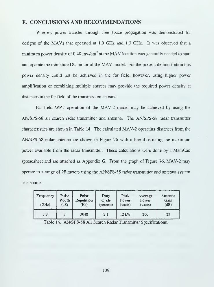
E. CONCLUSIONS AND RECOMMENDATIONS
Wireless power transfer through free space propagation was demonstrated for
designs of the MAVs that operated at 1.0 GHz and 1.3 GHz. It was observed that a
minimum power density of 0.40 mw/cm2at the MAV location was generally needed to start
and operate the miniature DC motor of the MAV model. For the present demonstration this
power density could not be achieved in the far field, however, using higher power
amplification or combining multiple sources may provide the required power density at
distances in the far field of the transmission antenna.
Far field WPT operation of the MAV-2 model may be achieved by using the
AN/SPS-58 air search radar transmitter and antenna. The AN/SPS-58 radar transmitter
characteristics are shown in Table 14. The calculated MAV-2 operating distances from the
AN/SPS-58 radar antenna are shown in Figure 76 with a line illustrating the maximum
power available from the radar transmitter. These calculations were done by a MathCad
spreadsheet and are attached as Appendix G. From the graph of Figure 76, MAV-2 may
operate to a range of 28 meters using the AN/SPS-58 radar transmitter and antenna system
as a source.
Frequency
(GHz)
Pulse
Width(uS)
Pulse
Repetition
(Hz)
Duty
Cycle
(percent)
PeakPower(watts)
Average
Power(watts)
AntennaGain
(dB)
1.3 7 3048 2.1 12 kW 260 23
Table 14. AN/SPS-58 Air Search Radar Transmitter Specifications.
139

.511.898558600
o MAV 2 ave wattsCu — — —
3 P
38"
58A ave
500-
400-
300
.0.319937
SPS-58 Antenna to MAV Range (meters)
Figure 76. M W-2 Required Transmitter Power verses Distance
From Source Antenna and Available AN/SPS-58 Radar Transmitter Power.
MAV_2_ave_watts is the MAV-2 Required Transmitter Power,
P58A ave is the available AN/SPS-58 Radar Transmitter Power.
140

VI. SUMMARY, CONCLUSIONS,AND RECOMMENDATIONS
A. SUMMARY
A receiving system for wireless power transfer (WPT) to a micro air vehicle (MAV)
has been demonstrated using commercially available off the shelf (COTS) hardware. The
receiving system was demonstrated to operate at two frequencies, 1.0 GHz and 1.3 GHz
with less than 2 watts of transmitted power. Required power density at the MAV was
determined to be less than 1 mW to demonstrate operation of a simple DC motor. A novel
approach was the use of a semi-omni directional antenna on the MAV, where power can be
received at any bearing relative to the MAV. Previous work had concentrated on the use of
large highly directional array receiving antennas, which would require a MAV to maintain a
particular orientation.
In this thesis, the remotely operated micro air vehicle applications of interest are
surveillance and urban warfare. This work could also be applied towards commercial
interests, such as the use of RF/Microwave powered identification (RF ID) tags for
inventory purposes. WPT could also be used to remotely operate many low powered
devices in which the use of on board batteries or power cabling is prohibited.
B. CONCLUSIONS
Wireless power transfer to a remote vehicle is possible and has been demonstrated.
Rectifier RF-to-DC conversion achieved a 30 percent efficiency using COTS hardware.
Higher efficiencies may be achieved using components with precisely specified
characteristics and tight tolerances. These components would include low forward
141

resistance diodes, such as Schottky GaAs diodes and high dielectric substrates with a
controlled relative permittivity.
The limiting factor for MAV range is the amount of RF power density provided at
the MAV location. This power density depends upon the transmitter power available and
the gain of the transmitting antenna. It is critical that the transmitted power be narrowly
confined in a tight beam pattern such that the spot size at the MAV site is not much greater
than the MAV itself. If this is the case, then much of the power will be absorbed by the
MAV antenna and converted to DC to power the MAV. Generally the larger the antenna
gain, the greater its size. Therefore transmitting antennas would likely be large. Fractal
techniques, however, may allow the design of smaller antennas [Ref 24].
Deploying multiple transmitter sites and combining the power at the MAV location
could reduce the need for a large transmitting antenna. Power levels would likely fluctuate
as some beams become blocked by obstacles or otherwise disturbed by the propagation path.
Reference 23 discusses the possibility of coherently combining the received power at the
MAV through a technique called "beam tagging." The beam tagging technique would
provide a stable maximum power at the MAV. Beam tagging requires feedback from the
MAV to the source transmitters and would add some complexity to the system. However, if
WPT is used solely to recharge an on-board battery, power fluctuations could be tolerated
by the MAV, and the need for a beam tagging system reduced.
C. SUGGESTIONS FOR FURTHER RESEARCH
The following areas are suggested for further investigation in order to provide more
efficient WPT to a MAV and reduce the weight of the MAV.
142

1. GaAs Schottky-barrier Diodes
This thesis concentrated on using the Hewlett Packard HSMS-2825 Silicon
Schottky-barrier diode in a surface mount package. It is well known that gallium arside
Schottky-barrier diodes (GaAs SBD) can provide a quicker diode with larger reverse current
blockage. The potential for greater RF-to-DC conversion efficiency exists when using
GaAs technology. The drawback to using GaAs is the cost and the possibility of easier
destruction of the semiconductor device either by high power microwave heating or by
electro-static discharge. Although silicon devices can also be affected by heating and static
discharge, silicon is not as sensitive to these effects. This thesis did not investigate the use
of GaAs diodes.
2. Additional Rectifier Circuit Configurations
Experiments and studies in Chapter IV indicated that multiple diodes be used in
parallel to provide high RF-to-DC conversion efficiency over a wider dynamic input power
range. In this thesis, a single Si-SBD SMT package was used that contained two diodes in
parallel. In order to place additional diodes in parallel, power splitting would have been
required in order to split the input RF power to the multiple diode packages. Other means to
achieve this without a power splitter requires that additional diodes be packaged in the same
SMT package or that much smaller packages be available.
An additional recommendation is to use a filter capacitor on the output side of the
SBD rectifier circuit. As discussed in Chapter IV, an output filter capacitor may increase the
RF-to-DC rectification efficiency. This was experimentally shown for input signals, such as
the pulsed CW input signals from a radar transmitter. Design of the filter capacitor with the
143

DC motor or battery loading could be achieved for greatest RF-to-DC conversion at the
transmitting frequency.
3. High Powered Sources
The WPT demonstration presented in this thesis was limited in the distance ofMAV
operation from the transmitting antenna. This limitation was due to the amount of
transmitter power that could be obtained from the amplifier available. Increased MAV
operation range could be demonstrated using a higher power source. Suggested sources
may include the AN/SPS-58 air search radar; however, it was shown earlier that the low
duty cycle of the pulsed CW signal significantly reduces the average signal power for a
extremely high peak power level.
Another potential transmitter source may be to use a very high power CW amplifier.
One such amplifier would be the Model 200T1G2 power amplifier available from Amplifier
Research of Souderton, PA. This power amplifier has an average power rating of 200 watts
CW over a frequency band of 1 to 2 GHz. According to Chapter V (Table 9 and Figure 63),
the increase in power is projected to power MAV operation 10 meters away from the
Microline/FXR transmitting horn.
A third possibility would be to demonstrate lower range MAV operation by using an
US Navy fleet operational radar that could support high duty cycles. One such system is the
AEGIS/SPY- 1 Radar System.
4. MAV Antenna Improvements
This thesis concentrated on developing a WPT demonstrator without regard to the
weight of the vehicle. Depositing a thin metal film or applying a conductive coating onto a
carbon fiber MAV body can yield a truly lightweight antenna. Lutronix has produced
144

several carbon fiber MAV bodies. Appendix H lists companies that could apply conductive
coatings or deposit thin metal films to a carbon fiber MAV body. Usually these coatings or
films are applied to shield plastic enclosed equipment from EMI. The manufacturers have
recommended using silver coating with a uniform 0.030 mm dry film thickness.
The as-built MAV copper antennas for this WPT demonstration were not optimized
for impedance matching as determined in the GNEC simulations of Chapter EI. It is
recommended that additional copper antennas be fabricated using the geometry of the
GNEC® simulations of Chapter HI. These additional antennas would be measured for input
impedance and the best geometry selected. This optimum geometry would be used as the
basis for depositing a thin metal film on a carbon fiber body. Evaluation of input impedance
would determine if the carbon fiber and thin film have a significant effect on antenna
properties.
5. Improved MAV DC Motor
The demonstration DC motor used is an inexpensive hobby motor with very low
torque and was likely to have low efficiency. Highly efficient, precision micro-motors that
can operate at high speed are available at a cost of roughly $200. One such DC motor is the
RE010-17 series rare Earth DC motor from Maxon Precision Motors of Burlingame, CA.
This motor at 10 mm in diameter and 27 mm long is significantly smaller than the
demonstration motor used. Due to its use of rare Earth Neodymium (NdFe) magnets, sinter
sleeve bearings and a planetary gearhead, this motor would likely have higher power
efficiency. The proposed motor operates at 19,000 rpm with an input power of less than
0.75 watt. Use of such a motor would obtain additional weight savings over the DC motor
145

used in this demonstration and could achieve enough rotor speed to provide lift to a
helicopter type MAV.
D. OTHER POTENTIAL INVESTIGATIONS
During microstrip rectifier testing, a significant power level for the second harmonic
of the transmitted signal was observed to originate from the diode. This effect is well
known and is sometimes used to form a frequency doubler. An operational MAV would
need to communicate back to the control station, and this second harmonic could be used to
transmit data from the MAV to the control station. This data could include information,
such as video and perhaps information for intelligent transmitter power management.
146
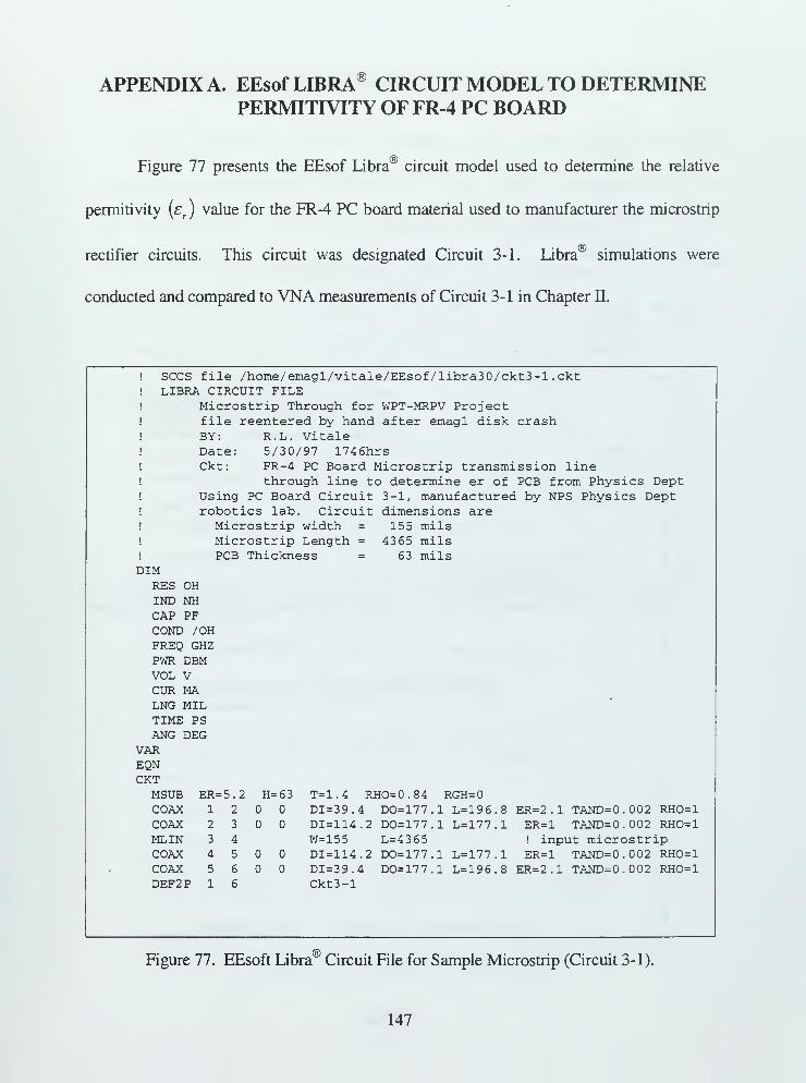
APPENDIX A. EEsof LIBRA® CIRCUIT MODEL TO DETERMINEPERMITIVITY OF FR-4 PC BOARD
.®Figure 77 presents the EEsof Libra circuit model used to determine the relative
permitivity (er ) value for the FR-4 PC board material used to manufacturer the microstrip
rectifier circuits. This circuit was designated Circuit 3-1. Libra® simulations were
conducted and compared to VNA measurements of Circuit 3-1 in Chapter II.
! SCCS file /home/emagl/vitale/EEsof/libra30/ckt3-l.ckt! LIBRA CIRCUIT FILE
Microstrip Through for WPT-MRPV Projectfile :reentered by hand after emagl disk crashBY: R.L. VitaleDate: 5/30/97 1746hrsCkt: FR-4 PC Board Microstrip transmission line
through line to determine er of PCB from Physics DeptUsing PC Board Circuit 3-1, manufactured by NPS Physics Deptrobot Lcs lab. Circuit dimensions areMicrostrip width = 155 milsMicrostrip Length = 4365 milsPCB Thickness = 63 mils
DIMRES OHIND NHCAP PFCOND /OHFREQ GHZPWR DBMVOL VCUR MALNG MILTIME PSANG DEG
VAREQNCKT
MSUB ER=5.2 H=63 T=1.4 RHO=0 . 84 RGH=0COAX 1 2 DI=39.4 DO=177.1 L=196.8 ER=2 . 1 TAND=0.002 RHO=lCOAX 2 3 DI=114.2 DO=177.1 L=177.1 ER=1 TAND=0.002 RHO=lMLIN 3 4 W=155 L=4365 ! input microstripCOAX 4 5 DI=114.2 DO=177.1 L=177 . 1 ER=1 TAND=0.002 RHO=lCOAX 5 6 DI=39.4 DO=177.1 L=196.8 ER=2 . 1 TAND=0.002 RHO=lDEF2P 1 6 Ckt3-1
,©Figure 77. EEsoft Libra Circuit File for Sample Microstrip (Circuit 3-1).
147

TERMPROCMODELSOURCEDCTR
dctrldctr2
FREQSWEEP 0.8 2 .8 0.02
POWERFILEOUT! S-parameter data to output file 'Circuit3-l.s2p"
Ckt3-1 TS SPAR Ckt3-l-52
OUTVAROUTEQNOUT
Ckt3-1 MAG[Z1] SCN ! Impedance to screenCkt3-1 Sll SC2 ! Smith ChartCkt3-1 DB[S11] GR1 Return Loss for through microstripCkt3-1 DB[S21] GR1 ! Transmission for DiodeCkt3-1 ANG[S11] GR2Ckt3-1 ANG [ S2 1
]
GR2GRID
! freqRANGE 0.8 2.8 0.2 ! GHz
! magnitudeGR1 -50.0 0.0 5.0 ! Db
Figure 77. EEsoft Libra® Circuit File for Sample Microstrip (Circuit 3-1) (continued).
148

APPENDIX B. MICROSTRIPLINE WIDTH CALCULATIONS
Figure 79 presents a MathCad® spreadsheet used to calculate the microstrip line
width required for a characteristic impedance of 50 ohms. A relative permittivity of 4.8 was
used. This value was the experimentally determined value for the fiberglass FR-4 PC board
used as the material to manufacturer the microstrip rectifier circuits. A simple 50 ohm
transmission through line was designed and designated as Circuit 4-1. Libra® simulations
were conducted and compared to VNA measurements of Circuit 4-1 in Chapter n.
1: Calculations of Microstrip Line Width.
Effective Relative Permitivity and Line Impedance
MAV Rectifier Circuit Design Parameters
Desired Characteristic Impedance:
Desired Operating Frequency:
Z 0m := 50 ohms
f :-l GHz
Material Parameters
Substrate Thickness:
Dielectric Constant:
Other Parameters
complex number:
Free space velocity (GHz):
thick :=— d := thick • 1000 d = 62.5 mils
16
£r
:= 4.8 experimentally determined.
Material is precoated,
fiberglass epoxy PC Board(FP4 Type).
j:=(-D
c := 3 10
0.5
cGHz := cGHz = 0.3
1 10
1A: Determine W/d ratio for 50 ohm microstrip line (Posar 4.206)
equation constants:
A :=Om
60
for W/d<2
W_over_d
for W/d>2
h, f 1 sr-l
/a23er+ l
B :=377 -ji
2Z 0m F.
8e'
e2A -2
W_over_d := —n
B - 1 - ln(2B - 1) +2-E,
ln(B - 1 ) +0.39 -0.61
W_over_d = 1.79 thus equation for W/d<2 is used.
Figure 78. Microstrip Width Calculations.
149

1 B: Determine effective permitivitv for microstrip line (Posar
)
Effective Dielectric Constant
(relative permittivity)
for 50 Q Microstrip Line
er+ 1 £
r- 1
£e
:=
£e
= 3.585
1 + 121
W over d
1 C: Determine guide wavelength (at desired frequency) for microstrip line
cGHzVelocity of propagation: V
P:=
0.5
Guide Wavelength in mils: X „cfri_ :=— ••
ustnpf Q \ i / \2.54
1000
Austri
= 6.238 »10 mils
Half Wavelength in mils:L:=
ustripL= 3.119 -10- mils
1 E. Measurements for 50 ohm microstrip line and check on Impedance
Width := W over d d Width = 111.896
* ustrip= 6.238 -10
;
mils
mils
Impedance Check (Posar 4.205 forW/d<1)
60 / 8 d WidthZ
0ustrip:=— ln
feh"+Td" Zoustrip^ 50467 ohms
Figure 78. Microstrip Width Calculations (Continued).
150

APPENDIX C. EEsof LIBRA® CIRCUIT MODEL FOR MICROSTRIPTHROUGH LINE
Figure 79 presents the EEsof Libra® circuit model developed to simulate the 50 ohm
microstrip line fabricated from FR-4 PC Board material with an unknown permittivity. This
circuit was designated Circuit 4-1. Libra® simulations were conducted and compared to
VNA measurements of Circuit 4-1 in Chapter n.
! SCCS file /home/emagl/vitale/EEsof /Iibra30/ckt4-l . ckt! LIBRA CIRCUIT FILE
Microstrip Through for WPT-MRPV Projectfile reentered by hand after emagl disk crashBY: R.L. VitaleDate: 6/5/97 1746hrsCkt: FR-4 PC Board Microstrip transmission line50 ohm transmission line
Using PC Board Circuit 4-1, manufactured by NPS Physics Deptrobotics lab. Circuit dimensions areMicrostrip width = 105 milsMicrostrip Length = 4325 milsPCB Thickness = 63 mils
DIMRES OHIND NHCAP PFCOND /OHFREQ GHZPWR DBMVOL VCUR MALNG MILTIME PSANG DEG
VAREQNCKT
MSUB ER=4.8 H=63 T=1.4 RHO=0 . 84 RGH=0COAX 12 DI=39.4 DO=177.1 L=196.8 ER=2 . 1 TAND=0. 002 RHO==1
COAX 2 3 DI=114.2 DO=177.1 L=177.1 ER=1 TAND=0. 002 RHO== 1
MLIN 3 4 W=105 L=4325 ! input microstripCOAX 4 5 DI=114.2 DO=177.1 L=177.1 ER=1 TAND=0
.
002 RHO==1COAX 5 6 DI=39.4 DO=177.1 L=196.8 ER=2 . 1 TAND=0
.
002 RHO==1DEF2P 1 6 Ckt4-1
.®Figure 79. EEsoft Libra Circuit Model for FR-4 Microstrip Through Line.
151

TERM
PROCMODELSOURCEDCTR
dctrldctr2
FREQSWEEP 0.8 2 .5 0.01
POWERFILEOUT! S-parameter data to output file " Circuit4-l-xx. s2p"
Ckt4-1 TS SPAR Ckt4-l-48OUTVAROUTEQNOUT
Ckt4-1 Sll SC2 ! Smith ChartCkt4-1 DB[S11] GR1 ! Return Loss for through microstripCkt4-1 DB[S21] GR1 ! Transmission for DiodeCkt4-1 ANG[S11] GR2Ckt4-1 ANG [ S2 1
]
GR2GRID
! freqRANGE 0.8 2.5 0.17 ! GHz
! magnitudeGR1 -50.0 0.0 5.0 ! dB
®Figure 79. EEsoft Libra Circuit Model for FR-4 Microstrip Through Line (continued).
152
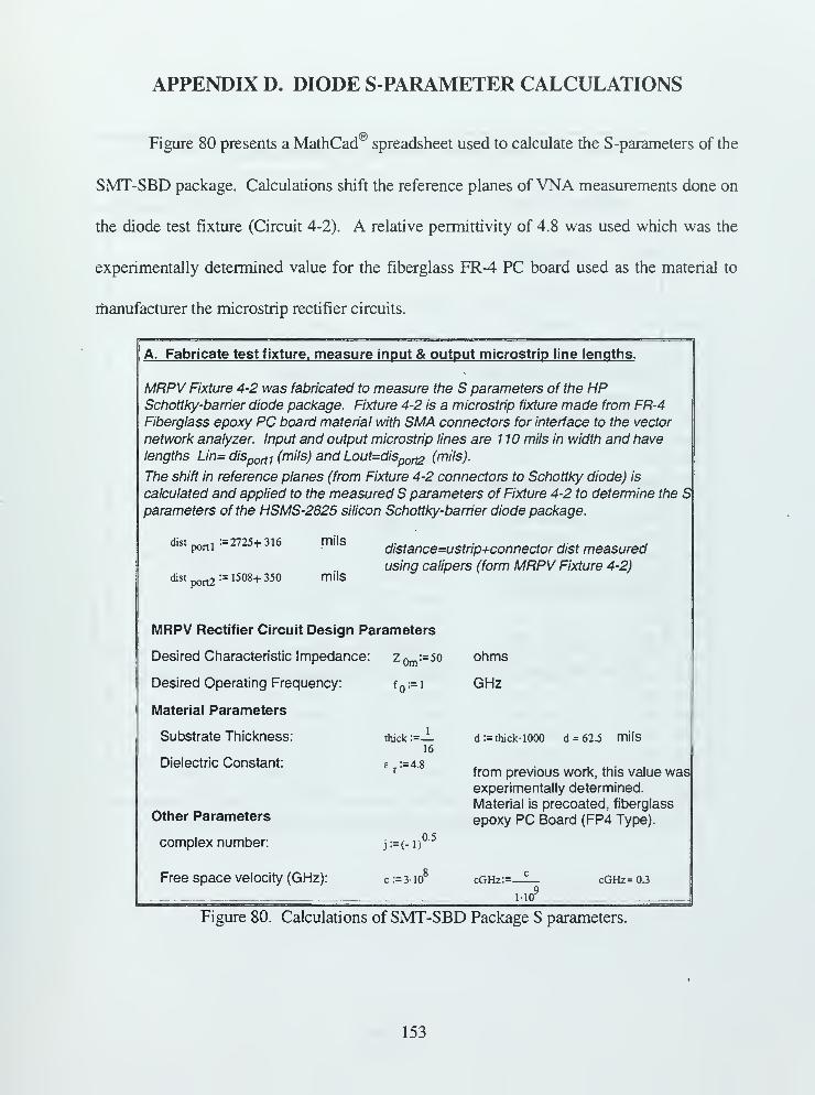
APPENDIX D. DIODE S-PARAMETER CALCULATIONS
Figure 80 presents a MathCad® spreadsheet used to calculate the S-parameters of the
SMT-SBD package. Calculations shift the reference planes of VNA measurements done on
the diode test fixture (Circuit 4-2). A relative permittivity of 4.8 was used which was the
experimentally determined value for the fiberglass FR-4 PC board used as the material to
manufacturer the microstrip rectifier circuits.
A. Fabricate test fixture, measure input & output microstrip line lengths.
MRPV Fixture 4-2 was fabricated to measure the S parameters of the HPSchottky-barrier diode package. Fixture 4-2 is a microstrip fixture made from FR-4
Fiberglass epoxy PC board materia! with SMA connectors for interface to the vector
network analyzer. Input and output microstrip lines are 1 10 mils in width and have
lengths Lin= disport i(mils) and Lout=disport2 (mils).
The shift in reference planes (from Fixture 4-2 connectors to Schottky diode) is
calculated and applied to the measured S parameters of Fixture 4-2 to determine the Sparameters of the HSMS-2825 silicon Schottky-barrier diode package.
dist^^ 2725+ 316
dist ^^ := 1508+ 350
mils
mils
distance=ustrip+connector dist measuredusing calipers (form MRPV Fixture 4-2)
MRPV Rectifier Circuit Design Parameters
Desired Characteristic Impedance: z^-so
Desired Operating Frequency:
Material Parameters
Substrate Thickness:
Dielectric Constant:
f :=l
thick :=
—
16
Other Parameters
complex number:
Free space velocity (GHz):
ohms
GHz
d:= thick- 1000 d = 62.5 mils
from previous work, this value wasexperimentally determined.
Material is precoated, fiberglass
epoxy PC Board (FP4 Type).
j:=(-D
c:=310!
0.5
cGHz:=-
1 10
cGHz= 0.3
Figure 80. Calculations of SMT-SBD Package S parameters.
153

B: Determine W/d for 50 ohm microstrip line (Posar 4.206)
equation constants: a :=p.- 377-,_
Zom l. r+ i«i r-i, ail *
60 4 2 er+l [' e
t 1 . 2 'z 0m'J*T
for W/d<2 for W/d>2
A - 8eA,_2
n
6,-1/B- l-ln(2B- 1) + ln(B-l) +
2-£r ^
0.39 -^ij2-A w over de - 2
W_over_d = 1.79 thus equation for W/d<2 is used.
Determine effective permitivitv for microstriD line (Posar
)
£e= 3.585
Effective Dielectric Constant
(relative permetivity)
for 50 Q. Microstrip Line£
£r+l e
r-l ,
c:= h •
2 2 j
1+12-^ W_over_d
Determine quide wavelenqth (at desired frequencv) for microstrio line (Posar
)
Velocity of propagation: cGHzVP
,=
0.5£
e
Guide Wavelength in mils: ._vp /100\ / 1 \ fiooo\
«* '
f [ 1 J U.54J i 1 )
Xustnp = 6.238-10
3mils
Figure 80. Calculations of SMT-SBD Package S parameters (Continued).
154

B. Measure the S parameters of MRPV Fixture 4-2 using VNA
S parameter measurements of MPRV diode fixture 4-2. S parameters are
measured at the ports of the board by a Hewlett Packard HP851 Vector Network
Analyzer. Measurements are dated 12/24/96. 1st Column is magnitude (dB), 2ndis phase in degrees
freq (GHz) Log Mag Phase Log Mag Phase Log Mag Phase Log Mag Phase
1 l_portl
0.80
0.86
0.93
1.00
1.07
1.14
1.20
1.27
1.34
1.41
1.48
1.54
1.61
1.68
1.75
1.82
1.88
1.95
2.02
2.09
2.16
2.22
2.29
2.36
2.43
2.50
-2.15 52.83
-2.25 29.40
-2.55 5.16
-2.87 -18.34
-3.09 -40.64
-3.42 -63.24
-3.89 -86.63
-4.21 - 109.36
-4.56 - 132.75
•5.17 -157.94
•5.62 176.67
•5.94 150.85
•6.30 124.16
•6.61 97.02
6.70 70.79
•6.91 44.73
7.07 19.50
7.23 -4.56
7.62 -28.30
7.88 -50.38
8.26 -71.85
8.63 -92.94
9.32 -113.95
10.08 -135.14
10.90 - 156.62
11.80 -178.30
S' 12'
-5.09 178.68
-4.88 157.16
-4.42 134.21
4.04 111.64
3.87 90.42
•3.63 68.80
3.28 46.51
•3.14 25.56
3.00 4.57
2.71 -17.67
2.54 -39.16
2.45 -60.18
•2.32 -81.70
•2.21 -103.28
2.18 -124.18
2.10 -145.61
•2.06 -166.78
•2.01 172.25
1.93 150.88
1.90 130.25
1.84 109.59
1.80 89.22
1.73 68.30
1.67 47.42
1.60 26.49
1.56 5.56
21
5.25 179.07
4.91 156.68
4.46 133.78
4.24 112.06
3.99 90.45
3.69 68.58
3.43 46.88
3.30 26.15
3.05 4.52
2.80 -17.35
2.64 -38.65
2.50 -60.16
2.37 -81.54
2.28 - 102.98
2.22 -124.18
2.16 - 145.56
2.13 - 166.60
2.09 172.40
2.04 151.29
1.99 130.69
1.94 110.11
1.89 89.73
1.81 68.84
1.74 48.02
1.68 27.06
1.63 6.13
221
-2.14 125.35
-2.36 105.10
-2.66 83.76
-2.85 63.55
-3.05 43.33
-3.36 22.72
-3.66 2.66
-3.83 -16.01
-4.20 -35.40
-4.63 -54.13
-4.93 -71.65
-5.28 -88.96
-5.62 - 105.55
-5.89 -121.74
•6.14 - 137.82
6.40 -154.12
6.63 -170.56
6.86 172.53
7.23 154.95
7.55 136.99
7.96 118.70
8.37 99.97
9.02 80.54
9.71 60.83
10.52 41.04
11.32 21.36
Figure 80. Calculations of SMT-SBD Package S parameters (Continued).
155

Part 3: Determine the S parameters for Hewlett Packard Schotkey Diodeby shifting reference planes
i:=l.. length (F11 portl)
n ;=1 - 2 Input_power := 15 dBm fl
2-71
us trip
ustnp
Find shift in reference plane(s) and then apply to measured data to get approximate
S values for the Schottky Diode at the input power level used (1 OdBm). Sparameters may however change depending upon the input power level.
Guide wavelength I) in microstrip
for frequencies measured:
.cGHz 100 1 1000
sweep.ustrip ^ j 05~T 254~TPlUrcrtl^e
Electrical length of input and output microstrip
180
Wavenumber 0)
2-Jt
sweep_ustnp _ j "
~
l.
2m'
dist
= dist
portl 'P sweep_ustrip J
'
port2 p sweep_ustrip jI
'
180
ll_portl
e j is the shift on input line
wheree2
is the shift on the output line
F n rtlare the operating frequencies
lines, convert to
0.800
0.860
0.930
1.000
1.070
1.140
1.200
1.270
1.340
1.410
1.480
1.540
1.610
1.680
1.750
1.820
1.880
1.950
2.020
2.090
2.160
2.220
2.290
2.360
2.430
2.500
sweep_ustnpj
degrees
140.392
150.921
163.205
175.490
187.774
200.058
210.588
222.872
235.156
247.440
259.725
270.254
282.538
294.823
307.107
319.391
329.920
342.205
354.489
366.773
379.058
389.587
401.871
414.155
426.440
438.724
85.777
92.210
99.716
107.221
114.727
122.232
128.665
136.171
143.676
151.182
158.687
165.121
172.626
180.132
187.637
195.143
201.576
209.081
216.587
224.092
231.598
238.031
245.537
253.042
260.548
268.053
Figure 80. Calculations of SMT-SBD Package S parameters (Continued).
156

S Parameters of diode inferred by shifting reference plane
Same Magnitudes New Angles
11m.1:=S'
11m.1'm.2
:=S'11 -,+ 26 l"m.2 'm
S ^i :=S'
l2m,\ SlW=S'^2+2K+92j
•21m.1
:=S' 21m, 1
'm.2
S22m,r
= S '22m, 1
S 22mi2:=S ,
221
S Parameters at Diode, use in Tou
' 0.80" "-2. 15 333.61"
0.86 -2.25 331.24
0.93 -2.55 331.57
1.00 -2.87 332.64
1.07 -3.09 334.91
1 l_portl=
1.14 Sll =-3.42 336.88
1.20 -3.89 334.55
1.27 -4.21 336.38
1.34 -4.56 337.56
1.41 -5.17 336.94
1.48 -5.62 696.12
1.54 -5.94 691.36
1.61 -6.30 689.24
1.68 -6.61 686.67
1.75 -6.70 685.00
1.82 -6.91 683.51
1.88 -7.07 679.34
1.95 -7.23 679.85
2.02 -7.62 680.68
2.09 -7.88 683.17
2.16 -8.26 686.27
2.22 -8.63 686.23
2.29 -9.32 689.79
2.36 -10.08 693.17
2.43 -10.90 696.26
.2 -50
.-11.80 699.15
:'^2+2-(e
lm+e
2j
+ 2-6
in Touchstone/Libra Program
12:
-5.09 631.02
-4.88 643.42
-4.42 660.05
-4.04 677.06
-3.87 695.42
-3.63 713.38
-3.28 725.02
-3.14 743.65
-3.00 762.23
-2.71 779.57
-2.54 797.66
-2.45 810.57
-2.32 828.63
-2.21 846.63
-2.18 865.31
-2.10 883.46
-2.06 896.21
-2.01 1.27M03
-1.93 1.29M03
-1.90 1.3M03
-1.84 1.3>103
-1.80 1.34»103
-1.73 1.36-103
-1.67 1.38M03
-1.60 1.40M03
-1.56 1.42M03
'21
-5.25 631.41
-4.91 642.94
-4.46 659.62
-4.24 677.48
-3.99 695.45
-3.69 713.16
-3.43 725.39
-3.30 744.24
-3.05 762.18
-2.80 779.89
-2.64 798.17
-2.50 810.59
-2.37 828.79
-2.28 846.93
-2.22 865.31
-2.16 883.51
-2.13 896.39
-2.09 1.27M03
-2.04 1.29M03
-1.99 1.31-103
-1.94 1.33M03
-1.89 1.34M03
-1.81 1.36M03
-1.74 1.38-103
-1.68 1.4O103
-1.63 1.42M03
22:
-2.14 296.90
-2.36 289.52
-2.66 283.19
-2.85 277.99
-3.05 272.78
"3.36 267.18
-3.66 259.99
-3.83 256.33
-4.20 251.95
-4.63 248.23
-4.93 245.72
-5.28 241.28
-5.62 239.70
-5.89 238.52
-6.14 237.45
-6.40 236.17
-6.63 232.59
-6.86 590.69
-7.23 588.12
-7.55 585.17
-7.96 581.90
-8.37 576.03
-9.02 571.61
-9.71 566.91
-10.52 562.14
-11.32 557.47
Figure 80. Calculations of SMT-SBD Package S parameters (Continued).
157

158

APPENDIX E. Si-SBD MODEL FILE FOR LIBRA®
This S parameter data file was used as a component in EEsof Libra microwave
circuit simulations to aid the design of impedance matching required for the Si-SBD rectifier
circuit. The Hewlett Packard HSMS-2825 dual surface mount Schottky-barrier diode
package is described.
! FILENAME hpdiodel .s2p Version: 1.1! P/N: HP Schottky Diode,
! By: R .L. Vitale Date: 5/30/97 18: 041 Reentered - original lost when emagl crashed
! BIAS CONDITIONS : none! NOTE : S -Parameters determined by VNA measuremtns with a re ference! Plane shift then applied. Numbers obtained from MathCad Spreadsheet' dated 1/16/97! VNA measurements taken on MRPV Diode Fixture 4--2.
! symbol freq-unit parameter- type data- format keywork impedance -ohms# GHZ S DB R 50
! freq dBSll ANGS11 dBS12 ANGS12 dBS21 ANGS21 dBS22 ANGS220.80 -2.15 333.61 -5.09 631.02 -5.25 631.41 -2.14 296 .90
0.86 -2.25 331.24 -4.88 643.42 -4.91 642.94 -2.36 289 .52
0.93 -2.55 331.57 -4.42 660.05 -4.46 659.62 -2.66 283 .19
1.00 -2.87 332.64 -4.04 677.06 -4.24 677.48 -2.85 277 .99
1.07 -3.09 334.91 -3.87 695.42 -3.99 695.45 -3.05 272 .78
1.14 -3.42 336.88 -3.63 713.38 -3.69 713.16 -3.36 267 .18
1.20 -3.89 334.55 -3.28 725.02 -3.43 725.39 -3.60 259 .99
1.27 -4.21 336.38 -3.14 743.65 -3.30 744.24 -3.83 256 .33
1.34 -4.56 337.56 -3.00 762.23 -3.05 762.18 -4.20 251 951.41 -5.17 336.94 -2.71 779.57 -2.80 779.89 -4.63 248 231.48 -5.62 696.12 -2.54 797.66 -2.64 798.17 -4.93 245 72.
1.54 -5.94 691.36 -2.45 810.57 -2.50 810.59 -5.28 241 281.61 -6.30 689.24 -2.32 828.63 -2.37 828.79 -5.62 239 701.68 -6.61 686.67 -2.21 846.63 -2.28 846.93 -5.89 238 521.75 -6.70 685.00 -2.18 865.31 -2.22 865.31 -6.14 237 45
1.82 -6.91 683.51 -2.10 883.46 -2.16 883.51 -6.40 236 171.88 -7.07 679.34 -2.06 896.21 -2.13 896.39 -6.63 232 591.95 -7.23 679.85 -2.01 1270.0 -2.09 1270.0 -6.86 590 692.02 -7.62 680.68 -1.93 1290.0 -2.04 1290.0 -7.23 588 12
2.09 -7.88 683.17 -1.90 1310.0 -1.99 1310.0 -7.55 585 17
2.16 -8.26 686.27 -1.84 1330.0 -1.94 1330.0 -7.96 581 902.22 -8.63 686.23 -1.80 1340.0 -1.89 1340.0 -8.37 576 032.29 -9.32 689.79 -1.73 1360.0 -1.81 1360.0 -9.02 571 612.36 -10.08 693.17 -1.67 1380.0 -1.74 1380.0 -9.71 566 912.43 -10.90 696.26 -1.60 1400.0 -1.68 1400.0 -10.52 562 142.50 -11.80 699.15 -1.56 1420.0 -1.63 1420.0 -11.32 557 47
Figure 81. EEsof Libra® Model for HP HSMS-2825 Si-SBD.
159

160

APPENDIX F. EEsof LIBRA® CIRCUIT MODEL FOR MICROSTRIPRECTIFIER CIRCUIT
®Figure 82 presents the EEsof Libra circuit model developed to simulate the
microstrip rectifier circuit using a 2-port S parameter input file and the characteristics of the
FR-4 PC Board with permittivity determined through VNA measurement and Libra®
® „:.simulations. This circuit was designated Circuit 4-2. Libra simulations were conducted
and compared to VNA measurements of Circuit 4-2 in Chapter II.
SCCS file /home/emagl/vitale/EEsof/libra30/fix4_2.cktLIBRA CIRCUIT FILE
Microstrip Shotkey Diode Circuit for WPT-MRPV ProjectModel of Circuit 4-2 constructed after buildout.!BY: R.L. VitaleDate: 7/10/97 1430hrsCkt: HP Schotkey Surface Mount Diode mounted on
50 ohm FR-4 PC Board Microstrip transmission line.Microstrip Schotkey Diode using data from VNA measurements onFixture 4-2 and calculating S parameters from shifting thereference plane. Calculations done using Mathcad spreadsheetdated 1/16/97.HP Schotkey Diode S Paramenter file: hpdiodel.s2p
DIMRES OHIND NHCAP PFCOND /OHFREQ GHZPWR DBMVOL VCUR MALNG MILTIME PSANG DEG
VAREONCKTMSUB ER= 4.8 H=70 T=1.4 RCOAX 1 2 DI=39.4COAX 2 3 DI=114.2MLIN 3 4 W=105S2P 4 5 hpdiodelMLIN 5 6 W=105DEF2P 1 6 Ckt4_2
RHO=0.84 RGH=0DO=177.1 L=196.8 ER=2 . 1 TAND=0.002 RHO=lDO=177.1 L=177.1 ER=1 TAND=0.002 RHO=lL=1500 ! input microstrip
! diode parameter fileL=2750 ! Output microstrip line
®Figure 82. EEsoft Libra Circuit File, Microstrip Rectifier Circuit (Circuit 4-2).
161

TERMCkt4_ 2 0.0 0.0 0.0 0.0 ! 50 ohm termination
PROCMODELSOURCEDCTR
dctrldctr2
FREQSWEEP 0.8 2 .8 0.05
POWERFILEOUTOUTVAROUTEQNOUT
Ckt4_2 Sll SC2 Smith ChartCkt4_2 DB[S11] GR1 Return Loss for Circuit 4-2
Ckt4_2 DB[S21] GR1 Transmission for Circuit 4-2
Ckt4_2 ANG[S11] GR2Ckt4_2 ANG [ S2 1
]
GR2GRID
! freqRANGE 0.8 2.8 0.2 ! range for plotGR1 -20.0 0.0 2.0 ! grid
Figure 82. EEsoft Libra® Circuit File, Microstrip Rectifier Circuit (Circuit 4-2) (continued)
162

APPENDIX G WPT PROPAGATION CALCULATIONS
Wireless power transfer propagation calculations for MAV using Microline horn antenna and AN/SPS-58 radar
transmitter. These calculations were conducted using a MathCad spreadsheet:
( 1 ) Distance to far field for Microline hom transmit antenna used in low power (MAV- 1 ) WPT demonstrations.
(2) Transmit power required to operate the MAV at various distances.
(3) Required average and peak power from AN/SPS-58 radar transmitter at various distances.
(1 ) Far Field Calculations for Microline/FXR Hom Antenna, used for Low Power Lab Transmission Far Field Calculation
Dimensions of Horn
(Height a := 41.2 cm
(Width) b:=
d:=
55.6 cm
(diagonal Ja2+ b
2
Frequencies of Interest
(Velocity)vp:=310
8
f:=
1.0
'
Frequencies L1.3
J
l»
^ *
A:=a 10
B:=bl0"
.-: A = 0.412 meters
B = 0.556 meters
f:=f-101-10"
1.3-10^
Wavelengths
Far Field Distance Calculation
rfar fiekT
2dfar field"
4.613
5.997meters
Antenna Gains
Receiving antennas (MAV) Gains from NEC simulations
G MAV lGHZ:=148dB G MAV 1.3GHZ :- L67 dB
Transmit Horn Antenna, from published specifications
G j:= 15 dB
MAV Recieve Antennas G 2:=
MAV 1GHZ
MAV 1.3GHZ
dB
163

Required input power to the MAV rectifier to turn the motor determined from rectifier measurements
Value based on results of testing of circuit 4-2 with small german dc motor (page 23 of lab book). MAV-1.3GHz Value
based on resultsfrom testing ofcircuit m7d-7 on page 78 oflab book
Pm lGHZ := ^ c^m
Pin 1.3GHZ:=15dB
R
Pin 1GHZ
Pin 1.3GHZ
dBm
Equation for required transmitted power to turn motor
trans'
4 * rfar field"
G rG 2*R
Easier to calculate in dB format calculate distance & frequency
/4-it-r
constant
Calculate power required in dBm
KdB== 20-logUfar fielc
P T :=K dB + P R~ G l~ G 2
Converting to mW and Watts
PTmW :=\ 1010
T W' P T_mW
i 1000 /
T mW :
T W
44.242
48.61
2.656'10
7.26M0
26.56
72.61
dBm
watts
(2) Required transmit power for MAV operation.
Calculate the required transmit power for MAV operation at various distances. We will be assuming that the far field
radiation equation is being used
Distances to be used
r:=(.l .3 .5 1 2 4 8 9 10 11 12 13 14 15 16 17 18 19 20 21)
>
'4-J[T\\
r := r
K^:* 20-logl Jlj = 0.3
p Tl:= K dBj + P R,
- G1_ G
2j
164

/4-JITK dB
2
:=
[
20M—\ X2= 0.231
P T2 :" K dB2
+ PP^, ~ G 1
_ G 22
Tl " 1 10.962 20.504 24.941 30.962 36.982 43.003MAV_1 := P T1
T2 "113.051 22.593 27.03 33.051 39.071 45.092MAV 2:=P T2
Plot Required Transmitter Power for Various Distances. Plot assumes that the MAV
requires 15 dBm at rectifier to operate motor.
S MAV_1
1 MAV_2
distance to MAV (meters)
165

(3) Required Peak Power from AN/SPS-58 Type Radar Transmitter at various distances
Calculate the required transmit power for MAV operation at various distances. We will be assuming that the far field
radiation equation is being used Compare to the output ofthe AN/SPS-58A Air Search Radar
AN/SPS-58 Transmitter Specifications
Maximum Transmitter Power
P 5gA := 12000 watts
Pulse Specifications and Duty Cycle
i := 7 10 seconds
prf := 3048 hz
Frequency & Wavelength
f mav 2:= 1.3 109
duty_cycle:= tprf duty_cycle= 0.021
5l:=
310°
f mav 2
k = 0.231
Average Power
P 58A_ave ;=P 58A duty-cycl( P 58A_ave = 256.032 watts
Antenna Gain
The SPS-58A uses a C/L Band horn antenna with C-Band reflector. Total Gain for antenna is specified as 23 dB,
which is 8dB greater than the Microline/FXR horn used earlier.
G sps58a :=23dB
Distances
Constant
i:= 1. 40 r58. := i
i
KdV=4-HT58
I = 0.231
Required Average Power from Transmitter (in dBm)
P T58_ave ;" K dB5g+ P^ ~ G sps58a " G 2
2
P T58_ave;
1 25.051 31.071 34.593 37.092 39.03 40.614 41.953 43.112MAV_2_ave:-
Convert average power to average power (watts) and to peak power (watts) for the radar transmitter
>
MAV 2 ave
MAV 2 ave watts:=10
10
\ 1000 /
MAV_2_peak_watts :=MAV_2_ave_watti
duty_cycle
P 58A ave:= P 58A ave
58A_ave
e58A_peak-
duty_cyd
166

Plot the resulting average and peak pulse power required at various distances from the AN/SPS-58 Radar transmitter
antenna in order to operate the MAV. It has been assumed that the MAV requires 15 dBm ofpower at the rectifier in order
to run the rectifier and DC motor combination. AN/SPS-58 average and peak power are plotted for comparison purposes
and as a means to determine maximum operating range ofthe MAV when using the AN/SPS-58 radar transmitter.
o MAV 2 ave_watts
600
1 p 58A_ave05
SPS-58 Antenna to MAV Range (meters)
MAV 2 peak wattscu
1 P 58A_peak
2.5*10
2*10 -
1.5-10 ~
15 20
r58
SPS-58 Antenna to MAV Range (meters)
40
167

168

APPENDIX H. LISTING OF POTENTIAL CONDUCTIVE COATINGOR THIN FILM SUPPLIERS
Table 15 presents a listing of potential suppliers that could help produce a light
weight MAV antenna for wireless power transfer. This antenna would be a carbon fiber
composite body with a highly conductive metallic outer surface. This conductive outer
surface could be applied either by depositing a thin film or by applying a conductive
coating. The Lutronix Corporation has produced MAV carbon fiber bodies, the vendors
listed in Table 15 would apply the applicable coating or deposit a thin conductive film.
Supplier Address and Contacts
Conductive Coatings Divisor
Chromium Corporation
308 Ellen Trout
Lufkin, TX 75904
(409) 633-6387
Thin Film, Vacuum, & Packaging
Department
The Advanced Manufacturing Processes
Laboratory (AMPL)Sandia National Laboratories
Kirkland AFBAlbuquerque, NMRobert L. Poole, Manager, (505) 845-9200
Janda Panitz (505) 845-8604
(JKPANIT@ scandia.gov)
John Zich (505) 845-8571
Advanced Thin Film Technology Thinfilms Manufacturing Facilities
Hillsborough Business Park
Bldg#13,6IlleneCourt
Belle Mead, NJ 08502
Motson Precision Printing and Finishing 1717 Bethlehem Pike
Flourtown,PA 19031-1110
(215) 233-0500
Thin Film Technology, Inc. 153 Industrial WayBuellton, CA 93427
(805) 688-4949
Precision Painting 1005 Orangethorpe Ave.
Anaheim, CA 92801
(714)630-0540
Table 15. Conductive Coating Suppliers for Carbon FiberMAV Body.
169

170

LIST OF REFERENCES
1. Brown, W. C, 'The Early History of Wireless Power Transmission and a
Discusssion of Transportronics for the Future," EEEE-MTTS Wireless Power
Transmission Workshop Notes, San Francisco, CA, 17 June 1996.
2. Brown, W.C., 'Thermionic Diode Rectifier," in Microwave Power Engineering,
Volume I, E.C. Okress, editor, pp. 295-298, Academic Press, New York, 1968.
3. Benford, J. and Dickinson, R., "Space Propulsion and Power Beaming using
Milimeter Systems," Society ofPhoto-Optical Instrumentation Engineers (SPIE),
San Diego, July 1995.
4. Kaya, Nobuyuki, "WPT'95 Workshop and Demonstration of Microwave Power
Transmission to Airship (Ether)," IEEE Microwave Theory and Technology (MTT-
S) International Symposium Workshop on Wireless Power Transfer, San Francisco,
1996.
5. Hawkins, Joe, 'The SABER (Semi-Autonomous BEam Rider) Microwave-Powered
Helicopter Project," IEEE Microwave Theory and Technology (MTT-S)
International Symposium Workshop on Wireless Power Transfer, San Francisco,
1996.
6. Jenn, D.C. and Vitale, R.L., "Wireless Power Transfer for a Micro Remotely Piloted
Vehicle," IEEE International Symposium on Circuits and Systems (ISCAS),
Monterey, CA, May 31 -June 3, 1998.
7. Jenn, D.C, "RPV," IEEE Potentials, Vol 16, No. 5, pp. 20-22, December 1997.
8. Proceeding ofthe First International Conference on Emerging Technologiesfor
Micro Air Vehicles, Georgia Institute of Technology, Atlanta, GA, February 19-20,
1997.
9. Gibson, T. B., "Propagation Loss Study and Antenna Design for the Micro-
Remotely Powered Vehicle," Master's Thesis, Naval Postgraduate School,
Monterey, CA, September 1995.
10. Sedra, A.S. and Smith, K.C., Microelectronic Circuits, Oxford University Press,
New York, NY, 1991.
1 1
.
George, R.H., "Solid State Power Rectifiers," in Microwave Power Engineering,
Volume I, E.C. Okress, editor, pp. 275-294, Academic Press, New York, 1968.
12. McSpadden, J.O., Yoo, T. and Chang, K., "Theoretical and Experimental
Investigation of a Rectenna Element for Microwave Power Transmission," IEEETransactions on Microwave Theory and Techniques, Vol. 40 No. 12, pp. 2359-55,
Dec 1992.
171

13. Pozar, D.M., Microwave Engineering, Addison-Wesley Publishing Company, Inc.,
Reading, MA, June 1990.
14. Balanis, C.A., Antenna Theory, Analysis and Design, John Wiley & Sons, NewYork, NY, 1982.
15. Collin, R.E., Antennas and Radiowave Propagation, McGraw-Hill, Inc., New York,
NY, 1985.
16. Brown, G.H. and Woodward, O.M., "Experimentally Determined Impedance
Characteristics of Cylindrical Antennas," Proceeding of Institute of Radio Engineers
(IRE), Vol. 33, pp. 257-262, 1945.
17. Harrington, R.F., Field Computation by Moment Methods, Macmillan, New York,
NY, 1968.
18. Nittany Scientic, Inc., GNEC-4 Version 1.1 Antenna Analysis Software User's
Manual, Nittany Scientific, Inc., 1700 Airline Highway, Suite 361, Hollister, CA,90523 USA, November 1997.
19. Burke, G.J., Numerical Electromagnetics Code - NEC-4, Method of Moments,
Lawrence Livermore National Laboratory, Report UCRL-MA- 109338, Livermore,
CA, January 1992.
20. Hewlett-Packard Company, Fundamentals of RF and Microwave Power
Measurements, Hewlett Packard Application Note 64-1 A, Hewlett-Packard
Company, Inc., Palo Alto, CA, June 1998.
21. Krause, P.C., Wasynczuk, O. and Sudhoff, S.D., Analysis ofElectric Machinery,
McGraw Hill Inc, New York, NY, 1986.
22. IEEE Standard C95.1-1991, IEEE Standard for Safety levels with Respect to HumanExposure to Radio Frequency Electromagnetic Fields, 3 kHz to 300 GHz, Institute
of Electrical and Electronic Engineers, Inc., 345 East 47th
Street, New York, NY,10017 USA, April 27, 1992.
23. Lee, Gary M., Barrett, Ronald, and Jenn, David, MRPV Design Study Final Report,
Lutronix Corportation, Del Mar, CA, 1996.
24. Yang, X., Chiochetti, J., Papadopoulous, D., and Susman, L., "Fractal Antenna
Elements and Arrays," Applied Microwave & Wireless, Vol 11, No. 5, pp. 34-46,
May 1999.
172

INITIAL DISTRIBUTION LIST
No. Copies
1. Defense Technical Information Center 2
8725 John J. Kingman Rd., STE 0944
Ft. Belvoir, VA 22060-6218
2. Dudley Knox Library 2
Naval Postgraduate School
411 Dyer Rd.
Monterey, CA 93943-5101
3. Chairman, Code EC 1
Department of Electrical and Computer Engineering
Naval Postgraduate School
Monterey, CA 93943-5121
4. Professor David C. Jenn, Code EC/Jn 3
Department of Electrical and Computer Engineering
Naval Postgraduate School
Monterey, CA 93943-5121
5. Professor Jeffery B. Knorr, Code EC/Ko 2
Department of Electrical and Computer Engineering
Naval Postgraduate School
Monterey, CA 93943-5121
6. Robert L. Vitale, Code EC 4
Department of Electrical and Computer Engineering
Naval Postgraduate School
Monterey, CA 93943-5121
7. Space and Naval Warfare System Command 2
Department of the NavyPMW-178Attn: CAPT. Connel
Washington, D.C. 20363-5100
8. Dr. Gary Lee 1
Lutronix Corporation
13627 Potofino Drive
Del Mar, CA 92014
173


oo 473npg ran i^ th hid cl11/02 22527-200 nle r


