design and implementation of semi-passive tunable micro machined rf filters
TRANSCRIPT
8/3/2019 Design and Implementation of Semi-Passive Tunable Micro Machined RF Filters
http://slidepdf.com/reader/full/design-and-implementation-of-semi-passive-tunable-micro-machined-rf-filters 1/4
Design and Implementation of Semi-Passive
Tunable Micromachined RF Filters
Gabriel M. Desjardins <[email protected]>
Abstract – This paper presents design
techniques for integrated RF filters in the 2 GHzrange. These filters use quasi-passive LC
topologies. Bond wires serve as the inductive
elements, while both fixed parallel platecapacitors and tunable micromachined
capacitors are used. The tunable capacitors are
designed for fabrication in the MUMPS
polysilicon micromachining process. The effects
of finite quality factors and bond wire
inductance variation on the transfer
characteristic of 3-pole low-pass filters are
discussed. Filter simulation and optimization is
used to determine the desired value for the
tunable capacitance.
I. Introduction
Filters for cellular and PCS frequencies are
typically implemented as discrete circuits using
components with high quality factors. Thesedevices are mechanically tuned or trimmed during
the manufacturing process to achieve the desired
transfer characteristic. However, in many wireless
applications, it is desirable to have a tunable filter
that can allow a single radio to support multiple
architectures without duplication of hardware. This
requires that the filter characteristic be changeable.
It is not difficult to design tunable filters usingstandard integrated circuit processes, but it is
difficult to achieve the high quality (Q) factors
necessary for high-frequency operation.
We seek to develop a tunable low-passfilter for RF and wireless applications that uses low
Q components. Tunable MEMS capacitors with
relatively low Q factors have been developed for
use in oscillators at cellular frequencies [4][5].
Section II presents methods for filter design using
low- or finite-Q components. Sections III and IV
describe the properties of bond wire inductors andtunable MEMS capacitors, respectively. Section V
discusses filter optimization by tuning the capacitor
value. Section VI describes test structures, and
Section VII concludes the paper.
II. Filter TheoryFilters were long ago characterized
according to their passband attenuation and phase
characteristics. Component values for common
filter prototypes, such as Butterworth and
Chebyshev, are often simply read from tables for
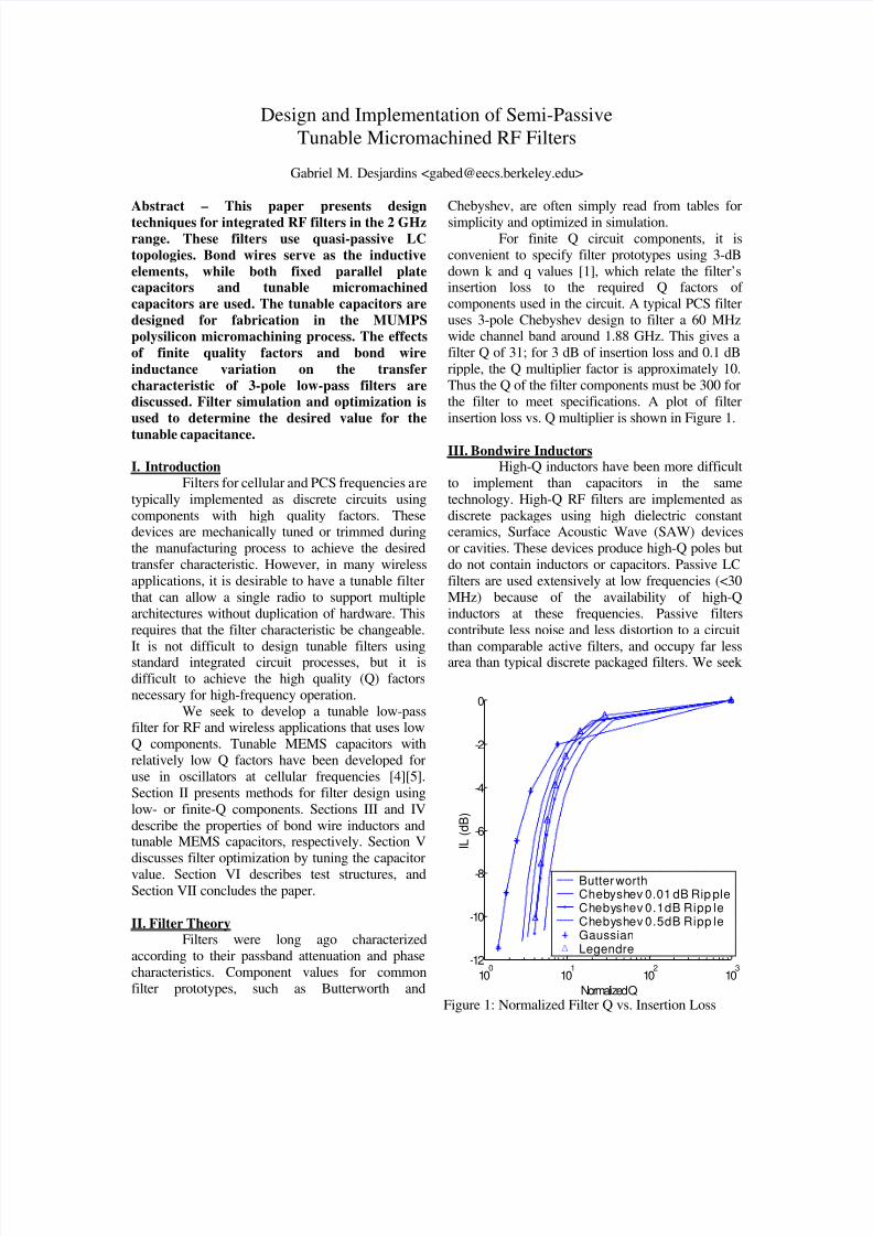
simplicity and optimized in simulation.For finite Q circuit components, it is
convenient to specify filter prototypes using 3-dB
down k and q values [1], which relate the filter’sinsertion loss to the required Q factors of
components used in the circuit. A typical PCS filter
uses 3-pole Chebyshev design to filter a 60 MHzwide channel band around 1.88 GHz. This gives a
filter Q of 31; for 3 dB of insertion loss and 0.1 dB
ripple, the Q multiplier factor is approximately 10.
Thus the Q of the filter components must be 300 for
the filter to meet specifications. A plot of filter
insertion loss vs. Q multiplier is shown in Figure 1.
III. Bondwire InductorsHigh-Q inductors have been more difficult
to implement than capacitors in the same
technology. High-Q RF filters are implemented as
discrete packages using high dielectric constantceramics, Surface Acoustic Wave (SAW) devices
or cavities. These devices produce high-Q poles but
do not contain inductors or capacitors. Passive LC
filters are used extensively at low frequencies (<30
MHz) because of the availability of high-Q
inductors at these frequencies. Passive filters
contribute less noise and less distortion to a circuit
than comparable active filters, and occupy far lessarea than typical discrete packaged filters. We seek
100
101
102
103
-12
-10
-8
-6
-4
-2
0
Normalized Q
I L ( d B )
B u t t e r w o r t hC h e b y s h e v 0 . 0 1 d B R i p p l eC h e b y s h e v 0 . 1 d B R i p p l eC h e b y s h e v 0 . 5 d B R i p p l eG a u s s i a nL e g e n d r e
Figure 1: Normalized Filter Q vs. Insertion Loss

8/3/2019 Design and Implementation of Semi-Passive Tunable Micro Machined RF Filters
http://slidepdf.com/reader/full/design-and-implementation-of-semi-passive-tunable-micro-machined-rf-filters 2/4
a high-frequency passive filter solution.CMOS-compatible passive inductors may
be implemented in several forms, including: 1)
circuit board spirals; 2) on-chip spirals; and 3) bond
wires. At GHz frequencies, on-board spirals can
have Q factors upwards of 200, but occupy
substantial area and require fabrication of circuit
boards [2]. Integrated on-chip spiral inductors are
smaller, but have Q factors on the order of 5 in the
frequency range of interest. Bond wire inductors
represent a trade-off: they have a Q an order of magnitude larger than on-chip spiral inductors at 1
GHz, and can be attached directly to an integratedcircuit. Unfortunately, the inductance of bond wires
is not well-controlled, so circuits that use bond
wires must allow for tuning other elements to
compensate for bond wire variation [3].
A. Bond Wire Quality Factor
Bond wires are frequently used to make
inductors because they have greater surface area perunit length than planar spiral inductors. This givesbond wires less resistive loss, and leads to a higher
quality factor. Bond wires also exhibit smallerparasitic capacitance to ground if they are placed
sufficiently far above any conducting planes. This
leads to a relatively simple physical model for bond
wires, since we may neglect the influence of other
conductors. The DC inductance of a bond wire is
given by:
Ll l
r =
−
µ
π0
2
20 75ln .
This gives an inductance of 2 nH for a standard 2
mm bond wire. The inductance value is weaklyfrequency-dependent, but varies on the order of 20-
25% depending on variations in length and themechanical quality of the bond.
For 1 mil Aluminum or Gold bond wires at
1 GHz, the skin depth is approximately 2.5 µm,which is small compared to the diameter of the wire
(25 µm). We assume that all of the current in thewire flows near its surface, giving an effective
resistance per unit length of 125 mΩ /mm at 1 GHz.
Rl
r
l
r
f = =
2 2
0
πδρ
µ
πρ
This does not take into account losses associated
with bond pads. The maximum inductor Q is:
Q L
Rr
l
r f = =
−
ωµ ρπ2
20 75 0ln .
The bond wire’s Q factor grows weakly with
increasing wire diameter, wire length, conductivityand operating frequency. Standard bond wires havea Q of approximately 50 at 1 GHz. The highest
achievable Q for 3 mil gold bond wires at 1.9 GHzis 284, though it is lower in practice.
IV. CapacitorsThe resonant frequency of an LC circuit is
inversely proportional to both L and C.If we are to
compensate for up to a 25% variation in the value
of our inductive element, we must be able to obtain
an equal variation in the capacitive element. We
0 2 4 6 8 1050
100
150
200
250
300
Length (mm)
Q
1 mil
3 mil
Figure 3: Bond wire Q vs. wire length at 1 GHz
0 2 4 6 8 100
2
4
6
8
10
12
Length (mm)
L ( n H )
3 mil1 mil
Figure 2: Bond wire inductance vs. length
1 1.5 2 2.5 3 3.5 4 4.5 550
100
150
200
250
300
350
400
450
Frequency (GHz)
Q
3 mil
1 mil
Figure 4: Bond wire Q vs. operating fr equency for 2
mm wire

8/3/2019 Design and Implementation of Semi-Passive Tunable Micro Machined RF Filters
http://slidepdf.com/reader/full/design-and-implementation-of-semi-passive-tunable-micro-machined-rf-filters 3/4
propose to use a tunable parallel plate air -gap
capacitor. The top plate rests on springs attached tothe substrate, while the bottom plate is attached
directly to the substrate. A mechanical diagram of the capacitor is shown in Figure 5. The maximum
variation in capacitance is 50%.
In combination, the springs have an
effective spring constant k. A bias voltage isapplied to the upper plate, which creates an
electrostatic force that pulls it towards the bottom
plate. The top plate moves downwards until it
reaches an equilibrium displacement ∆D given by:
0
2
1)(2)( 2223 =−∆+∆+∆ bV
k
Ad d d d d ε
A is the area of the plates and d is the gap between
the plates. The pull -down voltage is the voltage
required to pull the top plate down to ∆D=d/3:
ε A
kd V b
3
27
8=
For RF applications, the pull -down voltage should
be less than 2V. If we use a standard 2 mm long
bond wire, we require a nominal capacitance of 3.5
pF in order to implement filters with 2 GHz cutoff
frequencies. A 500
µm square plate
provides sufficientcapacitance; for 2V
operation, we require
a suspension with a
spring constant of 80
N/m.
Suspendedparallel plate
capacitors have been
fabricated in several
processes using
similar structures
[4][5]. We may
construct asuspended plate
capacitor using the
three-layer Poly
MUMPS process.
Figure 6 shows a top view of the capacitorstructure. The fixed plate is fabricated in Poly1
instead of Poly0 to minimize the likelihood of
electrical contact between the suspension anchors
and the fixed plate. We model the suspended plate
as a cantilever fixed at both ends, which is
equivalent to two sets of series springs in parallel
with each other. The combined spring constant is:
3
3
3
2
)2 / (
3
L
EWt
L
EI k ==
Where E is the Young’s Modulus of Polysilicon,and W, t and L are the width, thickness and length
of the suspension. For a 36 µm wide by 77 µm longsuspension arm, the spring constant is 79.8 N/m
and the pull-down voltage is 2.12 V. Holes occupyapproximately 10% of the surface area of the
suspension arm; this allows for a wider arm while
simultaneously reducing its mass, but red ucing its
spring constant and resulting in a pull -down voltage
closer to 2V.
V. Filter Analysis and Expected Results
We implement a 3rd
-order LC filter using
two capacitors to eliminate the coupling betweeninductors. The circuit diagram is shown in Figu re 7.
One capacitor is implemented using the designdescribed in the previous section, while the other
capacitor can be a fixed parallel -plate design. The
bond wire Q is on the order of 50, while the tunable
capacitor Q is approximately 10; the Q of the fi xed
capacitor is sufficiently high that it may be ignored.
The relatively high sheet resistance of polysilicon
reduces the Q of the tunable capacitor compared to
Aluminum [5] or other metals. The inductor is
modeled as an LR series circuit; a two-dimensional
solver [6] gives a parallel resistance of
approximately 0.005 Ω to ground for a 500 µm
square poly-poly air-gap capacitor. This does notconsider the effects of etching holes in both plates.
Figure 8 shows the filter tuning process.
The top transfer characteristic is obtained for idealinductors and capacitors, nominally 2.9 nH and 3.5
pF. The inductor value is reduced by 20%, giving
the incorrect bottom transfer function. The
capacitor value is then tuned to produce the middle
characteristic, with less than 3 dB insertion loss and
a corrected cutoff frequency. Since the inductor and
capacitors vary substantially and their respective Q
factors are not predictable, this tuning process is
most easily performed by fabricating the circuit and
measuring each component. These measurementscan be back-substituted into a circuit simulator todetermine the optimal tuned capacitance value.
Figure 5: Tunable Capacitor
Figure 6: Tunable Capacitor
(top view)
Figure 7: Three -pole Low-pass Filter
8/3/2019 Design and Implementation of Semi-Passive Tunable Micro Machined RF Filters
http://slidepdf.com/reader/full/design-and-implementation-of-semi-passive-tunable-micro-machined-rf-filters 4/4
VI. Test StructuresThere are numerous degrees of freedom in
designing the varactor structure. The capacitance
and pull-down voltage are functions of the
capacitor area, the size of the suspension andintrinsic material properties. The structure and
orientation of holes in the two plates greatly
influences the circuit parasitics. The size of the
capacitors limits the range of t est structures
(including bond pads, each capacitor measures at
least 800 µm by 600 µm). An entire wafer maycontain fewer than 16 capacitors.
Pull-down voltage is determined primarily
by the suspension spring constant, given in Section
IV, which is a function of suspension size. The
pull-down voltage for a capacitor with a 36 µmwide suspension as a function of the suspension
length is shown in Figure 9. Its thickness is fixed,and we fix its width and fabricate structures with
lengths of 80, 100 and 140 µm to obtain differentspring constants. The test structures consist of foursets of capacitors with the above suspension
lengths. Each set of capacitors uses different sized
etch holes (4, 6, 8 and 10 µm) in order to determinethe optimal hole size to release the structure. The
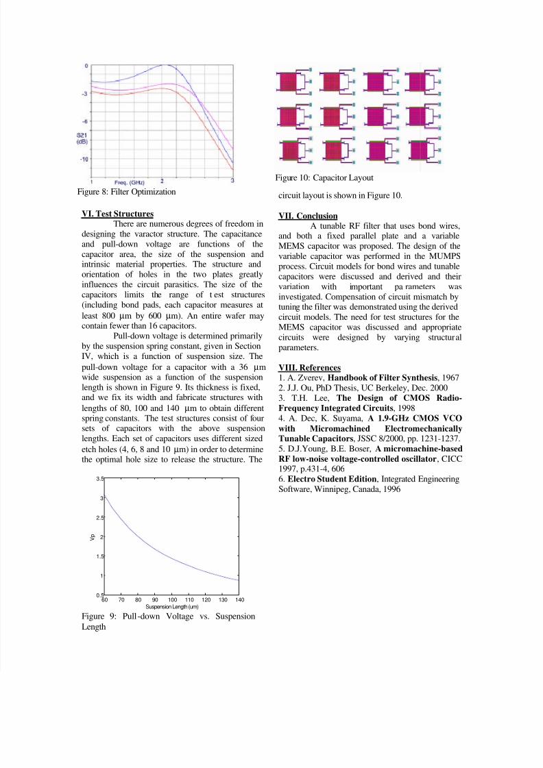
circuit layout is shown in Figure 10.
VII. ConclusionA tunable RF filter that uses bond wires,
and both a fixed parallel plate and a variable
MEMS capacitor was proposed. The design of the
variable capacitor was performed in the MUMPS
process. Circuit models for bond wires and tunablecapacitors were discussed and derived and their
variation with important pa rameters was
investigated. Compensation of circuit mismatch bytuning the filter was demonstrated using the derived
circuit models. The need for test structures for the
MEMS capacitor was discussed and appropriate
circuits were designed by varying structural
parameters.
VIII. References
1. A. Zverev, Handbook of Filter Synthesis, 1967
2. J.J. Ou, PhD Thesis, UC Berkeley, Dec. 2000
3. T.H. Lee, The Design of CMOS Radio-
Frequency Integrated Circuits, 19984. A. Dec, K. Suyama, A 1.9-GHz CMOS VCO
with Micromachined ElectromechanicallyTunable Capacitors, JSSC 8/2000, pp. 1231-1237.
5. D.J.Young, B.E. Boser, A micromachine-based
RF low-noise voltage-controlled oscillator, CICC1997, p.431-4, 606
6. Electro Student Edition, Integrated Engineering
Software, Winnipeg, Canada, 1996
Figure 8: Filter Optimization
Figure 10: Capacitor Layout
60 70 80 90 100 110 120 130 1400.5
1
1.5
2
2.5
3
3.5
Suspension Length (um)
V
p
Figure 9: Pull-down Voltage vs. Suspension
Length