design and implementation of a udp/ip offload engine
TRANSCRIPT
DESIGN AND IMPLEMENTATION
OF A UDP/IP OFFLOAD ENGINE
Burak BATMAZ Master of Science Thesis
Electrical and Electronics Engineering Program
August, 2015

JÜRİ VE ENSTİTÜ ONAYI
Burak Batmaz’ın “Design and Implementation of a UDP/IP Offload
Engine” başlıklı Elektrik-Elektronik Anabilim Dalı Elektronik Bilim Dalındaki,
Yüksek Lisans Tezi 24.08.2015 tarihinde, aşağıdaki jüri tarafından Anadolu
Üniversitesi Lisansüstü Eğitim-Öğretim ve Sınav Yönetmeliğinin ilgili maddeleri
uyarınca değerlendirilerek kabul edilmiştir.
Adı Soyadı İmza
Üye (Tez Danışmanı) : Doç. Dr. Atakan DOĞAN …………..
Üye : Doç. Dr. Hakan Güray ŞENEL …………..
Üye : Yrd. Doç. Dr. M. Mustafa ATANAK …………..
Anadolu Üniversitesi Fen Bilimleri Enstitüsü Yönetim Kurulu’nun ……………..
tarih ve …………….. sayılı kararıyla onaylanmıştır.
Enstitü Müdürü

ABSTRACT
Master of Science Thesis
DESIGN AND IMPLEMENTATION OF A UDP/IP OFFLOAD ENGINE
Burak BATMAZ
Anadolu University
Graduate School of Sciences
Electrical and Electronics Engineering Program
Supervisor: Assoc. Prof. Dr. Atakan DOĞAN
2015, 66 pages
Network packet processing in high data rates has become a major problem
especially for the processors. Fortunately, this thesis offers a solution to this
problem by means of an IP core that provides the hardware acceleration of
UDP/IP protocol stack together with few other network protocols. Furthermore,
the IP core is equipped with PCI Express (PCIe) interface so as to communicate
with applications running on PC. Consequently, a processor core deals with only
the data processing, while the IP core takes care of the packet processing as per
the protocol. The design and implementation of the IP core are verified and tested
on a Xilinx XUVP5-LX110T board. Moreover, its area utilization and supported
features are compared against several competitive designs from the literature.
According to these results, the proposed IP core is proved to be a usefull one for
those applications that require a hardware-accelerated network protocol stack for
data communication.
Keywords: FPGA, UDP/IP, PCIe, Network Protocols, Digital Design
i

ÖZET
Yüksek Lisans Tezi
UDP/IP OFFLOAD ENGINE TASARIMI VE GERÇEKLENMESİ
Burak BATMAZ
Anadolu Üniversitesi
Fen Bilimleri Enstitüsü
Elektrik-Elektronik Mühendisliği Anabilim Dalı
Danışman: Doç. Dr. Atakan DOĞAN
2015, 66 sayfa
Yüksek hızlarda ağ paketlerinin işlenmesi özellikle işlemciler için bir
problem haline gelmeye başlamıştır. Bu tez bu probleme UDP/IP protocol
yığınıyla birlikte diğer birkaç ağ protokolünün donanım ile hızlandırılmasını
sağlayan bir IP çekidek vasıtasıyla çözüm sunmaktadır. Ayrıca, IP çekidek
bilgisayarda çalışan uygulamalarla haberleşebilmesi için PCI Express (PCIe)
arayüzü ile donatılmıştır. Sonuç olarak, IP çekidek ilgili protokol gereğince paket
işleme ile ilgilenirken, işlemci çekirdeği sadece veri işleme ile ilgilenir. IP
çekirdeğin tasarımı ve gerçeklemesi Xilinx XUVP5-LX110T kartı üzerinde
doğrulanmış ve test edilmiştir. Ayrıca, alan kullanımı ve desteklenen özellikleri,
literatürde yer edinmiş benzer çalışmalarla karşılaştırılmıştır. Bu sonuçlara göre,
sunulan IP çekirdeğin veri iletişimi için donanım ile hızlandırılmış ağ protokol
yığını gerektiren uygulamalar için kullanışlı olduğu kanıtlanmıştır.
Anahtar Kelimeler: FPGA, UDP/IP, PCIe, Ağ protokolleri, Sayısal Tasarım
ii

ACKNOWLEDGEMENTS
I would like to thank my advisor Assoc. Prof. Dr. Atakan DOĞAN for his
guidence and support during my study.
I would like to thank love of my life Zeynep for her support,
encouragement, patience and unwavering love. I thank my parents for their
endless support.
Burak Batmaz
August, 2015
iii
TABLE OF CONTENTS
ABSTRACT .............................................................................................................i
ÖZET ...................................................................................................................... ii
ACKNOWLEDGEMENTS ................................................................................ . iii
TABLE OF CONTENTS ..................................................................................... iv
LIST OF FIGURES ........................................................................................... vii
LIST OF TABLES ...............................................................................................ix
ABBREVIATIONS ............................................................................................... x
1. INTRODUCTION ............................................................................................ 1
1.1. Motivation .................................................................................................... 1
1.2. Thesis Goals and Contributions .................................................................... 1
1.3. Thesis Organization ...................................................................................... 2
2. BACKGROUND ............................................................................................... 3
2.1. OSI Layers .................................................................................................... 3
2.1.1. Physical layer................................................................................... 3
2.1.2. Data link layer ................................................................................. 4
2.1.2.1. Media access control ....................................................................... 4
2.1.2.2. Logical link control ......................................................................... 4
2.1.3. Network layer .................................................................................. 4
2.1.4. Transport layer................................................................................. 5
2.1.5. Session layer .................................................................................... 5
2.1.6. Presentation layer ............................................................................ 5
2.1.7. Application layer ............................................................................. 6
2.2. User Datagram Protocol ............................................................................... 6
2.3. Internet Protocol ........................................................................................... 7
2.4. Dynamic Host Configuration Protocol ....................................................... 10
2.5. Internet Control Message Protocol ............................................................. 13
2.6. Address Resolution Protocol ...................................................................... 14
2.7. Ethernet ....................................................................................................... 16
iv
2.8. PCI Express ................................................................................................ 17
2.9. Network Packet Processing Overview ....................................................... 18
2.10. Related Work ........................................................................................ 22
3. SYSTEM DESIGN .......................................................................................... 25
3.1. Overall System Architecture ...................................................................... 25
3.2. Xillybus ...................................................................................................... 26
3.2.1. PCIe Interface IP core ................................................................... 26
3.2.2. Xillybus IP core ............................................................................. 27
3.2.3. Xilinx FIFOs .................................................................................. 28
3.3. MAC IP Core .............................................................................................. 28
3.4. Custom FIFOs ............................................................................................ 30
3.5. API for Offload Engine .............................................................................. 30
4. OFFLOAD ENGINE ...................................................................................... 33
4.1. Channel Selector ......................................................................................... 36
4.2. UDP Tx ....................................................................................................... 38
4.3. IP Tx ........................................................................................................... 41
4.4. Arbitrator .................................................................................................... 43
4.5. IP Rx ........................................................................................................... 44
4.6. UDP Rx ...................................................................................................... 46
4.7. DHCP IP Core ............................................................................................ 47
4.8. ICMP IP Core ............................................................................................. 49
4.9. ARP IP Core ............................................................................................... 50
4.10. Configuration Component ..................................................................... 51
5. IMPLEMENTATION AND EXPERIMENTAL RESULTS ..................... 52
5.1. Implementation Results .............................................................................. 52
5.2. Experimental Results .................................................................................. 53
5.2.1. Throughput results ......................................................................... 54
5.2.2. ICMP verification .......................................................................... 57
5.2.3. DHCP verification ......................................................................... 58
5.2.1. ARP verification ............................................................................ 59
v

6. CONCLUSIONS ............................................................................................. 61
REFERENCES .................................................................................................... 63
vi
LIST OF FIGURES
2.1. OSI and TCP/IP reference models ................................................................... 3
2.2. UDP header structure ....................................................................................... 6
2.3. Pseudo-header for UDP checksum computing ................................................ 7
2.4. IPv4 header structure........................................................................................ 8
2.5. DHCP packet format ...................................................................................... 11
2.6. DHCP message types ..................................................................................... 12
2.7. DHCP state diagram ....................................................................................... 13
2.8. ICMP header structure for the ping messages................................................ 13
2.9. ARP packet structure...................................................................................... 15
2.10. Ethernet packet structure .............................................................................. 16
2.11. PCIe layers ................................................................................................... 18
2.12. Operational structure of the network stack .................................................. 19
2.13. CPU load and throughput comparison between Latona and GNIC ............. 20
2.14. CPU Utilization of Tx and Rx sides at 2.4 GHz system .............................. 20
2.15. CPU Utilization of network stack processing at 1 Gbps .............................. 21
2.16. Operational structure of our design .............................................................. 21
3.1. System architecture of the IP core proposed .................................................. 25
3.2. Overview of Xillybus architecture ................................................................. 26
3.3. MAC IP core architecture .............................................................................. 29
3.4. API implementation architecture ................................................................... 31
4.1. Offload Engine architecture ........................................................................... 33
4.2. Alachiotis et al. IP core architecture .............................................................. 34
4.3. Löfgren et al. IP core architecture .................................................................. 35
4.4. Herrmann et al. IP core architecture .............................................................. 35
4.5. Channel Selector architecture ........................................................................ 36
4.6. FSM state diagram of Channel Select ............................................................ 37
4.7. Host data format ............................................................................................. 38
4.8. UDP Tx architecture ...................................................................................... 39
4.9. FSM state diagram of UDP Tx....................................................................... 40
4.10. IP Tx architecture ......................................................................................... 41
4.11. FSM state diagram of IP Tx ......................................................................... 42
vii
4.12. Arbitrator architecture .................................................................................. 44
4.13. IP Rx architecture ......................................................................................... 45
4.14. FSM state diagram of IP Rx ......................................................................... 46
4.15. UDP Rx architecture .................................................................................... 47
4.16. FSM state diagram of UDP Rx .................................................................... 47
4.17. FSM state diagram of DHCP ....................................................................... 48
4.18. ICMP architecture ........................................................................................ 49
4.19. ARP architecture .......................................................................................... 51
4.20. Configuration architecture ........................................................................... 51
5.1. Experimental setup for the system tests ......................................................... 54
5.2. Command window output - an example throughput test ............................... 55
5.3. The impact of packet size on throughput ....................................................... 55
5.4. Wireshark output of an example throughput test ........................................... 57
5.5. ICMP functionality verification command window output ........................... 57
5.6. ICMP functionality verification wireshark output ......................................... 58
5.7. Packet transmission with no IP configuration ................................................ 59
5.8. Packet transmission with manual IP configuration ........................................ 59
5.9. Packet transmission with DHCP configuration.............................................. 59
viii

LIST OF TABLES
4.1. Implemented protocols in our design and related works ............................... 34
5.1. Synthesis results of the design ....................................................................... 52
5.2. Implementation details comparison ............................................................... 53
ix
ABBREVIATIONS
API : Application programming interface
ARP : Address Resolution Protocol
BOOTP : Bootstrap Protocol
CPU : Central processing unit
CRC : Cyclic redundancy check
CSMA/CD : Carrier Sense Multiple Access with Collision Detection
DHCP : Dynamic Host Configuration Protocol
Din : Data input
DLLP : Data Link Layer Packet
DNS : Domain Name System
ECRC : End-to-end CRC
EMAC : Ethernet MAC
FPGA : Field Programmable Gate Array
FSM : Finite State Machine
FSMD : Finite State Machine with Datapath
HTTP : Hyper-Text Transfer Protocol
ICMP : Internet Control Message Protocol
IFG : Inter-frame Gap
IHL : Internet Header Length
IP : Internet Protocol
IP Core : Intellectual Property Core
LAN : Local Area Network
LCRC : Link CRC
LLC : Logical Link Control
LUT : Look-up Table
MAC : Media Access Control
MTU : Maximum Transmission Unit
NIC : Network Interface Card
OS : Operating system
OSI : Open System Interconnection
PCIe : PCI Express
x

RARP : Reverse Address Resolution Protocol
SFD : Start of Frame Delimiter
SMTP : Simple Mail Transfer Protocol
TCP : Transmission Control Protocol
TLP : Transaction Layer Packet
TOE : TCP Offload Engine
TOS : Type of Service
TTL : Time to Live
UDP : User Datagram Protocol
UOE : UDP Offload Engine
VoIP : Voice over IP
xi

1. INTRODUCTION
Motivation
Nowadays many applications need high-speed data transfers which are
enabled by a stack of network protocols. These protocols are traditionally
implemented by means of a software running on the host central processing unit
(CPU); and they may require encapsulation, decapsulation, checksum computing,
memory copying, etc., all of which are briefly called as packet processing. In
high-speed networks, on the other hand, the packet processing requires an
extensive amount of CPU power, which results in less CPU cycles for
applications running on the host. Fortunately, the computing power of CPU
spared for the packet processing can be saved provided that the packet processing
tasks are delagated to a so-called offload engine that can perform them on the
network adapter. An offload engine can be implemented with a network processor
and firmware, ASICs or FPGAs, or a mixture of these. Within the scope of thesis,
a set of network protocols that are enough to provide data communication in
Internet will be offloaded to hardware on a FPGA.
An offload engine purely implemented in hardware is usefull for system-on-
chip (SoC) systems as well. A processor or an application logic in a SoC system
can exploit a hardware-based offload engine for the data communication without
the neeed for running the software-implemented network processes.
Thesis Goals and Contributions
Motivated by aferomentined facts, the main goals of this thesis are
designing a gigabit speed Offload Engine for the network protocol stack which
includes User Datagram Protocol (UDP) [1], Internet Protocol (IPv4) [2], Internet
Control Message Protocol (ICMP) [3], Dynamic Host Configuration Protocol
(DHCP) [4] and Address Resolution Protocol (ARP) [5], equipping this Offload
Engine with a PCIe [6] interface for those applications running on a PC and with
1
Ethernet [7] for the network connection and implementing and verifying it on
Virtex 5 FPGA-based development board.
Different from the previous studies, this thesis contributes to the literature in
a few dimensions:
• Offload Engine is the first to use a third party PCIe IP core to interface
with user applications.
• It is the first to implement DHCP protocol on hardware.
• It can simultaneously support multiple data streams from different
applications.
• It has a pipelined design for achieving higher data througputs and clock
rates.
Thesis Organization
Organization of the thesis is as follows: Section 2 gives the background
information about the implemented protocols in Offload Engine, Ethernet and
PCIe interface. In Section 3, the overall system design is given, a few thirdy party
IP cores used in the design are introduced and an application programming
interface for the design is presented. In Section 4, Offload Engine is described in
detail. Section 5 presents the synthesis results of Offload Engine, compares them
with the previous designs from the literature. It further includes the functional
verification of the implemented network protocols and the experimental results for
the achieved data throughputs under different scenarios. In Section 6, conclusions
and future avenues of research are given.
2
2. BACKGROUND
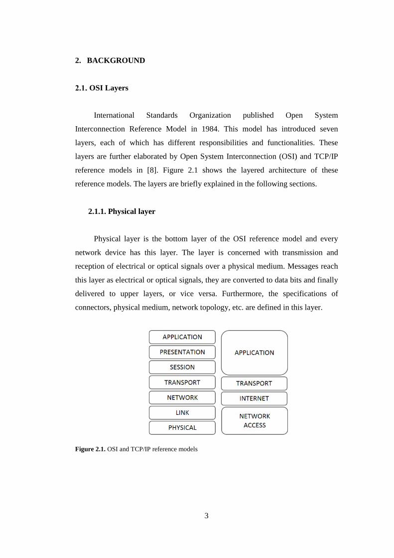
OSI Layers
International Standards Organization published Open System
Interconnection Reference Model in 1984. This model has introduced seven
layers, each of which has different responsibilities and functionalities. These
layers are further elaborated by Open System Interconnection (OSI) and TCP/IP
reference models in [8]. Figure 2.1 shows the layered architecture of these
reference models. The layers are briefly explained in the following sections.
2.1.1. Physical layer
Physical layer is the bottom layer of the OSI reference model and every
network device has this layer. The layer is concerned with transmission and
reception of electrical or optical signals over a physical medium. Messages reach
this layer as electrical or optical signals, they are converted to data bits and finally
delivered to upper layers, or vice versa. Furthermore, the specifications of
connectors, physical medium, network topology, etc. are defined in this layer.
Figure 2.1. OSI and TCP/IP reference models
3

2.1.2. Data link layer
Data Link layer is the second layer of the OSI reference model, and it is
composed of two sublayers, namely Media Access Control and Logical Link
Control.
2.1.2.1. Media access control
Media Access Control (MAC) sublayer is placed between Physical layer
and Logical Link Control sublayers. This layer is primarily responsible for
providing a data communication channel among the network nodes that share a
common medium. In order to avoid collisions in the shared medium, MAC
sublayer runs a medium access control algorithm such as Carrier Sense Multiple
Access with Collision Detection (CSMA/CD). In addition, MAC sublayer deals
with framing as well. Before sending a packet, MAC layer appends a preamble,
MAC source and destination addresses, etc. at the head of packet and a cyclic
redundancy check (CRC) at the tail of packet. While receiving packets, their
CRCs are calculated and checked for possible errors.
2.1.2.2. Logical link control
Logical Link Control (LLC) sublayer is a bridge between Network layer and
Media Access Control sublayer. LLC adds two bytes to the head of any packet
received from Network layer to specify the packet type (IP or ARP). These two
bytes are known as LLC header. For the packets that are received from MAC
sublayer, LLC header field is controlled and they are delivered to the appropriate
protocol.
2.1.3. Network layer
Network layer is the third layer of the OSI reference model. The most
commonly used network protocol is IPv4, and also preferred in this study. Its
4

main tasks include forwarding, routing, and logical addressing, fragmentation of
those packets bigger than the maximum transmission unit (MTU) and
defragmentation of the received fragmented packets.
2.1.4. Transport layer
Transport layer is the fourth layer of OSI reference model. Mostly used
transport layer protocols are Transmission Control Protocol (TCP) and User
Datagram Protocol (UDP). TCP [9] is a reliable and connection oriented protocol.
It can provide end-to-end reliable packet transmission, end-to-end flow control
and end-to-end congestion control. Unlike TCP, UDP [1] is an unreliable protocol
and does not guarantee that packets will be delivered to their destination hosts.
Applications that require low latency packet transmission such as Domain Name
System (DNS), Voice over IP (VoIP) use UDP protocol. Both TCP and UDP need
to deal with multiplexing/demultiplexing of packets as well. In this study, UDP is
implemented as Transport layer protocol.
2.1.5. Session layer
Session layer is the fifth layer of the OSI reference model. As the name
implies, this layer is responsible for establishing, managing and terminating
sessions between application processes on the same or different machines. Sockets
are placed in this layer. A network socket is an application programming interface
(API) that helps network programmers to start sessions between applications and
use the lower layer protocols without knowing their implementation details.
2.1.6. Presentation layer
Presentation layer is the sixth layer of the OSI reference model.
Applications can use different syntaxes and this layer transforms them to a
common format. When receiving data, it transforms the data back to the format
5

that application uses. Data compression and encryption are also handled by this
layer.
2.1.7. Application layer
Application layer is the highest layer of the OSI reference model. This layer
offers several protocols to applications to use the network. For example, web
browser applications use Hyper-Text Transfer Protocol (HTTP) [10] and e-mail
applications use Simple Mail Transfer Protocol (SMTP) [11] in this layer.
User Datagram Protocol
User Datagram Protocol (UDP) is a connectionless, unreliable transport
layer protocol [1]. UDP does not establish a connection between hosts, so there is
no packets for setting up a connection or closing it. UDP is an unreliable protocol
and it gives no guarantee for packet delivery. Thus, applications are responsible
for detecting duplicate packets. UDP has no congestion control or flow control
either. Therefore, applications need to keep their sending rate under control so that
they will not congest the network or overwhelm the receiver side. Because of
these inherent features, UDP is preferred by applications that are time critical and
do not require reliability.
Each protocol in the network stack encapsulates the data with a header.
Similarly, UDP header structure is in Figure 2.2 [1].
According to Figure 2.2, UDP header consists of four fields, each of which
is 16-bit long:
Figure 2.2. UDP header structure [1]
6
• Source Port: Each application on a computer has a port number that is
associated with it so that different applications can send and receive data
at the same time. Transport layer protocols multiplex outgoing packets
and demultiplex incoming packets according to these port numbers. So,
this defines the port number of a sender application.
• Destination Port: This defines the port number of a receiver application.
If a client is sending UDP packets to a server, destination port numbers
are usually well known.
• Length: This field carries the length in bytes of UDP header (8 byte) and
Application Data.
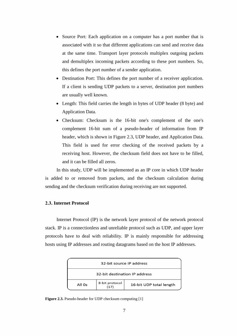
• Checksum: Checksum is the 16-bit one's complement of the one's
complement 16-bit sum of a pseudo-header of information from IP
header, which is shown in Figure 2.3, UDP header, and Application Data.
This field is used for error checking of the received packets by a
receiving host. However, the checksum field does not have to be filled,
and it can be filled all zeros.
In this study, UDP will be implemented as an IP core in which UDP header
is added to or removed from packets, and the checksum calculation during
sending and the checksum verification during receiving are not supported.
Internet Protocol
Internet Protocol (IP) is the network layer protocol of the network protocol
stack. IP is a connectionless and unreliable protocol such as UDP, and upper layer
protocols have to deal with reliability. IP is mainly responsible for addressing
hosts using IP addresses and routing datagrams based on the host IP addresses.
Figure 2.3. Pseudo-header for UDP checksum computing [1]
7

Each device connected to a network has a unique IP address, which is 32-bit
for IPv4 and 128-bit long for IPv6. Since IPv4 is the most commonly used
Internet protocol in today’s network [2], it is chosen to be implemented on
hardware by this thesis. Figure 2.5 shows the IPv4 header structure, and its fields
are explained below:
• Version: It is 4-bit field that specifies the version of IP protocol. For our
design, this field is fixed to 4 since it supports only IPv4.
• Internet Header Length (IHL): It is 4-bit field that indicates the total
length of IP header. This number must be multiplied by four to find out
the header byte count in bytes. If Options field is not used, this field is set
to 5 since the standard IPv4 header is 20 bytes long, which is the case in
our design.
• Total Length: This 16-bit field represents the total number of data bytes
in IP datagram, which results in the maximum data size of 64 Kbytes.
However, if the maximum transfer unit (MTU) of network does not
support such big datagrams, IP has to fragment them into smaller chunks.
In our design, IP fragmentation is not supported, which requires that
upper layer protocol need to send smaller packets than the MTU of
network. Furthermore, if a fragmented packet is received by our receiver,
it will be dropped.
Figure 2.4. IPv4 header structure [2]
8
• Type of Service (TOS): This 8-bit field is used to specify the quality of
service desired, such as low latency, high throughput or high reliability
for IP datagrams. In our design, TOS field is not used and set to zero.
• Identification: This 16-bit field is used for identifying the fragmented IP
datagrams. In our study, this field is also set to 0 when sending and
ignored when receiving a datagram because of the lack of the
fragmentation support.
• Flags: It is a 3-bit field related to the datagram fragmentation. Thus,
Flags field is set to 0 in our design.
• Fragment Offset: It is 13 bits long field and carries an offset value if
datagram is fragmented. This field is set to 0 as well.
• Time to Live (TTL): This 8-bit field determines the lifetime of a
datagram. It is set by the sender and is decremented by one every time it
traverses a hop. When TTL value becomes zero, datagram is discarded
and an ICMP massage is sent back to the sender of this datagram, which
prevents them to get stuck in the network indefinitely. TTL is set to 128
by default in our design.
• Protocol: IP provides IP level demultiplexing through this 8-bit field that
indicates which protocol is used in the upper layer. In our design, only
two upper layer protocols exist: Code 1 tells IP to deliver this message to
ICMP and code 17 to UDP.
• Header Checksum: This field is 16 bits long and used for error checking.
In our design, it is calculated and placed in IP header when sending
datagrams; but, Header Checksum is not checked by our receiver, since
MAC Layer checks the CRC of all received frames.
• Source Address: This 32-bit field represents the IP address of the sender.
• Destination Address: This 32-bit field represents the IP address of the
receiver. In our design, IP receiver checks this field of any datagram, and
if it is not equal to the IP address of receiver, incoming datagrams are
simply discarded. However, the broadcast packets will not be dropped.
9
• Options: This field is variable length and not present in every datagram,
since it is optional. It represents a list of options such as security or
record route. It is not used in our design.
In this study, IPv4 will be implemented as an IP core in which IP header is
added to or removed from UDP and ICMP packets.
Dynamic Host Configuration Protocol
Dynamic Host Configuration Protocol (DHCP) [4] which runs over UDP is
a network protocol that provides static or dynamic IP addresses from a DHCP
server to DHCP clients on the network. A DHCP client is a user that requests an
IP address from a DHCP server when it connects to the network or boots its
computer. This protocol was first released in 1993, and then, the current DHCP
definition for IPv4 was released in 1997. DHCP is built on Bootstrap Protocol
(BOOTP) [12] which was the protocol that had taken the place of Reverse
Address Resolution Protocol (RARP).
DHCP packet format is shown in Figure 2.5. DHCP has a standard format
except for Options field. The fields of DHCP packet are explained below.
• Operation Code: This is an 8-bit field to indicate the type of packets.
Clients send request packets with code 1 and server sends reply packets
with code 2. Since our design implements a DHCP client, it is code 1.
• Hardware Type: This 8-bit field is set to 1 for Ethernet.
• Hardware Address Length: It specifies the length of MAC address in 8-
bit field and is fixed at 6 by default.
• Hop Count: This field is set to 0 by client.
• Transaction Identifier: This field holds a 32-bit number defined by client
to identify the packets that belong to different DHCP transactions. This
field is set to Hexadecimal 000000BB in our design.
• Number of Seconds: It is filled by clients and represents the seconds
passed from the beginning of the request process. This field is set to zero
in our design.
10

Figure 2.5. DHCP packet format [4]
• Flags: This 16-bit field is set 0 or 1 by a client while sending a request if
it expects a broadcast reply or unicast reply from the server, respectively.
In our design, it is fixed at 0 for the unicast reply.
• Client IP Address: If client has already taken an IP address and now
renewing or rebinding it, it fills this 32-bit field with its own IP address.
Otherwise, it fills with zeros even if it is requesting a specific IP address.
• Your IP Address: Server fills this 32-bit field with the IP address that has
been assigned to a client.
• Server IP Address: This 32-bit field holds the IP address of the server
that client will use for the renewing and rebinding processes. This field is
not used and set to zero in our design.
• Gateway IP Address: This 32-bit field holds the IP address of a relay
agent. A relay agent is required if a client and server are placed on
different networks. It is not used and fixed at zero in our design.
• Client Hardware Address: It represents the MAC address of a client.
Since this field is 16 bytes long and MAC address is 6 bytes long, it is
padded with zeroes.
11
• Server Name: This 64-byte field is usually not used, but server can put its
name here. It is not used and set to zero in our design.
• Boot File Name: This 128-byte field is usually not used. It is filled with
zeros in our design.
• Options: This variable length field is used for basic DHCP operations.
There are over 100 different DHCP options, and some of them are
included in most of DHCP messages. For example, Option 53 is included
in every DHCP message since it represents the message type. In our
design, DHCP Message Type, Client Identifier and Requested IP Address
options are used.
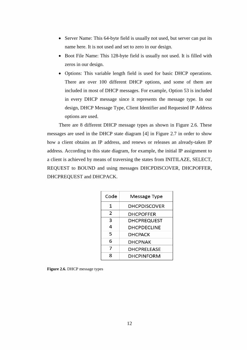
There are 8 different DHCP message types as shown in Figure 2.6. These
messages are used in the DHCP state diagram [4] in Figure 2.7 in order to show
how a client obtains an IP address, and renews or releases an already-taken IP
address. According to this state diagram, for example, the initial IP assignment to
a client is achieved by means of traversing the states from INITILAZE, SELECT,
REQUEST to BOUND and using messages DHCPDISCOVER, DHCPOFFER,
DHCPREQUEST and DHCPACK.
Figure 2.6. DHCP message types
12
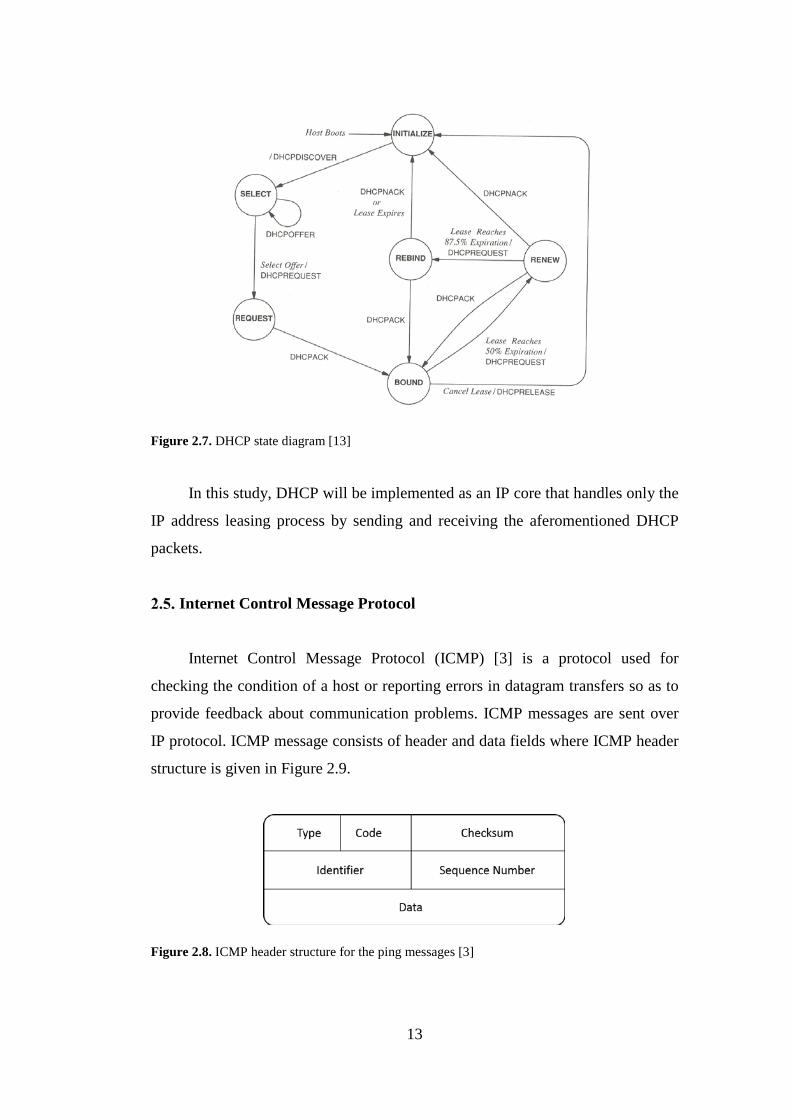
Figure 2.7. DHCP state diagram [13]
In this study, DHCP will be implemented as an IP core that handles only the
IP address leasing process by sending and receiving the aferomentioned DHCP
packets.
Internet Control Message Protocol
Internet Control Message Protocol (ICMP) [3] is a protocol used for
checking the condition of a host or reporting errors in datagram transfers so as to
provide feedback about communication problems. ICMP messages are sent over
IP protocol. ICMP message consists of header and data fields where ICMP header
structure is given in Figure 2.9.
Figure 2.8. ICMP header structure for the ping messages [3]
13
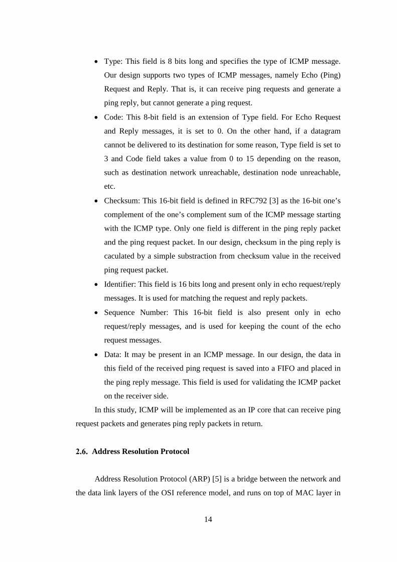
• Type: This field is 8 bits long and specifies the type of ICMP message.
Our design supports two types of ICMP messages, namely Echo (Ping)
Request and Reply. That is, it can receive ping requests and generate a
ping reply, but cannot generate a ping request.
• Code: This 8-bit field is an extension of Type field. For Echo Request
and Reply messages, it is set to 0. On the other hand, if a datagram
cannot be delivered to its destination for some reason, Type field is set to
3 and Code field takes a value from 0 to 15 depending on the reason,
such as destination network unreachable, destination node unreachable,
etc.
• Checksum: This 16-bit field is defined in RFC792 [3] as the 16-bit one’s
complement of the one’s complement sum of the ICMP message starting
with the ICMP type. Only one field is different in the ping reply packet
and the ping request packet. In our design, checksum in the ping reply is
caculated by a simple substraction from checksum value in the received
ping request packet.
• Identifier: This field is 16 bits long and present only in echo request/reply
messages. It is used for matching the request and reply packets.
• Sequence Number: This 16-bit field is also present only in echo
request/reply messages, and is used for keeping the count of the echo
request messages.
• Data: It may be present in an ICMP message. In our design, the data in
this field of the received ping request is saved into a FIFO and placed in
the ping reply message. This field is used for validating the ICMP packet
on the receiver side.
In this study, ICMP will be implemented as an IP core that can receive ping
request packets and generates ping reply packets in return.
Address Resolution Protocol
Address Resolution Protocol (ARP) [5] is a bridge between the network and
the data link layers of the OSI reference model, and runs on top of MAC layer in
14
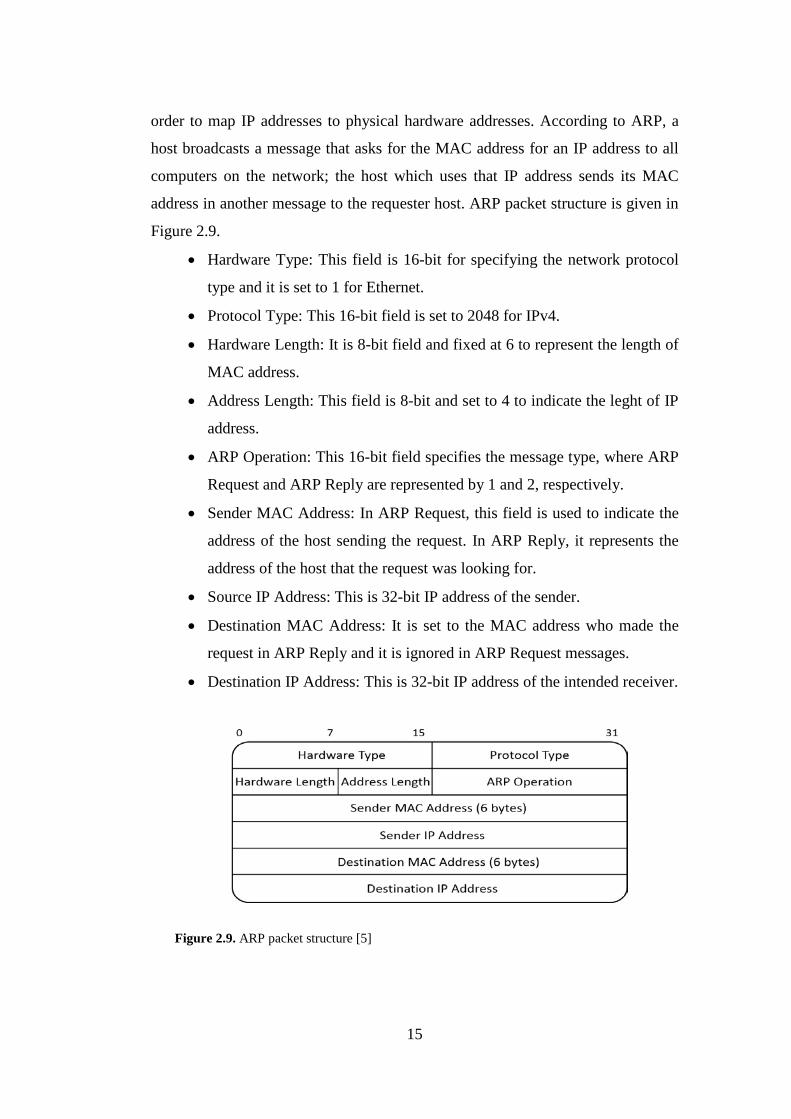
order to map IP addresses to physical hardware addresses. According to ARP, a
host broadcasts a message that asks for the MAC address for an IP address to all
computers on the network; the host which uses that IP address sends its MAC
address in another message to the requester host. ARP packet structure is given in
Figure 2.9.
• Hardware Type: This field is 16-bit for specifying the network protocol
type and it is set to 1 for Ethernet.
• Protocol Type: This 16-bit field is set to 2048 for IPv4.
• Hardware Length: It is 8-bit field and fixed at 6 to represent the length of
MAC address.
• Address Length: This field is 8-bit and set to 4 to indicate the leght of IP
address.
• ARP Operation: This 16-bit field specifies the message type, where ARP
Request and ARP Reply are represented by 1 and 2, respectively.
• Sender MAC Address: In ARP Request, this field is used to indicate the
address of the host sending the request. In ARP Reply, it represents the
address of the host that the request was looking for.
• Source IP Address: This is 32-bit IP address of the sender.
• Destination MAC Address: It is set to the MAC address who made the
request in ARP Reply and it is ignored in ARP Request messages.
• Destination IP Address: This is 32-bit IP address of the intended receiver.
Figure 2.9. ARP packet structure [5]
15

ARP keeps a table which saves the IP addresses and their corresponding
MAC addresses. By this way, host does not send an ARP request for every packet,
which reduces the network traffic and speeds up the data transfers. If ARP cache
becomes full and a new ARP Reply is received, then the least recently used IP and
MAC address couple is replaced with the new one.
In this study, ARP will be implemented as an IP core in which ARP Request
and ARP Reply packets are both received and sent, ARP cache is saved for the
MAC addresses. ARP Request and ARP Reply packets are received, processed
and delivered to the related component by ARP receive sub component. ARP
requests are created in ARP sender by an order from the IP Tx component and
ARP replies are created for received ARP requests. The received MAC addresses
are kept in a cache in the ARP control&cache sub component to prevent sending
ARP request for each IP packet.
Ethernet
Ethernet is the most widely used Local Area Network (LAN) protocol [7]. It
was originally developed in 1980 and standardized by IEEE as IEEE 802.3 in
1983. A standard Ethernet packet structure is given in Figure 2.10.
• Preamble: It is 7 bytes of bit sequence of “10101010” for the
synchronization on the receiver side.
• Start of Frame Delimiter (SFD): This is 1 byte bit sequence of
“10101011”. It tells the receiver that the part coming after this byte is the
actual frame.
• Destination/Source MAC Address: It represents the hardware address of
the receiver and sender, respectively.
Figure 2.10. Ethernet packet structure [7]
16
• Ether Type: This field represents the protocol that is included in the
Ethernet frame. Hexadecimal 0800 specifies an IP datagram and 0806
specifies an ARP packet.
• Data: This field carries a packet of upper layer protocol. This field needs
to be minimum 46 bytes. As a result, if data is smaller than 46 bytes,
Data field is padded with zeros.
• Cyclic Redundancy Check (CRC): This 32-bit checksum is calculated by
means of the 32-bit cyclic redundancy check algorithm, and it is used for
error detection on the receiver side. The CRC computation includes the
destination and source MAC addresses, ether type and data fields.
It is required that idle time called as Inter-frame Gap (IFG) between two
successive frames must be present. The standard minimum IFG is 96 “bit times”.
This time gap naturally changes with the Ethernet line speed, e.g., 9.6 µs for 10
Mbit/s, 0.96 µs for 100 Mbit/s and 96 ns for the Gigabit Ethernet.
Ethernet uses Carrier Sense Multiple Access/Collision Detection
(CSMA/CD) protocol to physically monitor the traffic on the channel and prevent
any possible collision. CSMA/CD is placed on the Media Access Control (MAC)
sub-layer of the Ethernet. This protocol allows multiple computers to share a
channel. If two computer try to send packets at the same time, this causes a
collision. If a collision occurs, computers try to send again after a randomly
selected time, which is known as the exponential back-off.
In this study, Ethernet will be implemented by a third party IP core in which
preamble, SFD and CRC are added to the packets to be sent and received packets
are checked for error and delivered to upper layers.
PCI Express
PCI Express (PCIe) is the third generation I/O bus used to interconnect
peripheral devices in computing or communication systems [6]. PCIe has replaced
the second generation buses PCI, AGP and PCI-X, and it is backward compatible
with PCI and PCI-X. In PCIe jargon, a connection between two devices over PCIe
is called a link, and a pair of signals in both directions is called a lane. A link can
17
consist of either x1, x2, x4, x8, x16 or x32 lanes. The transmission rate of a lane is
5 Gbits/s (2.5 Gbits/s in each direction). PCIe uses the 8B/10B encoding, which
results in the fact that 250 Mbytes/s (2 Gbits/s) per lane is the highest achievable
throughput in a direction.
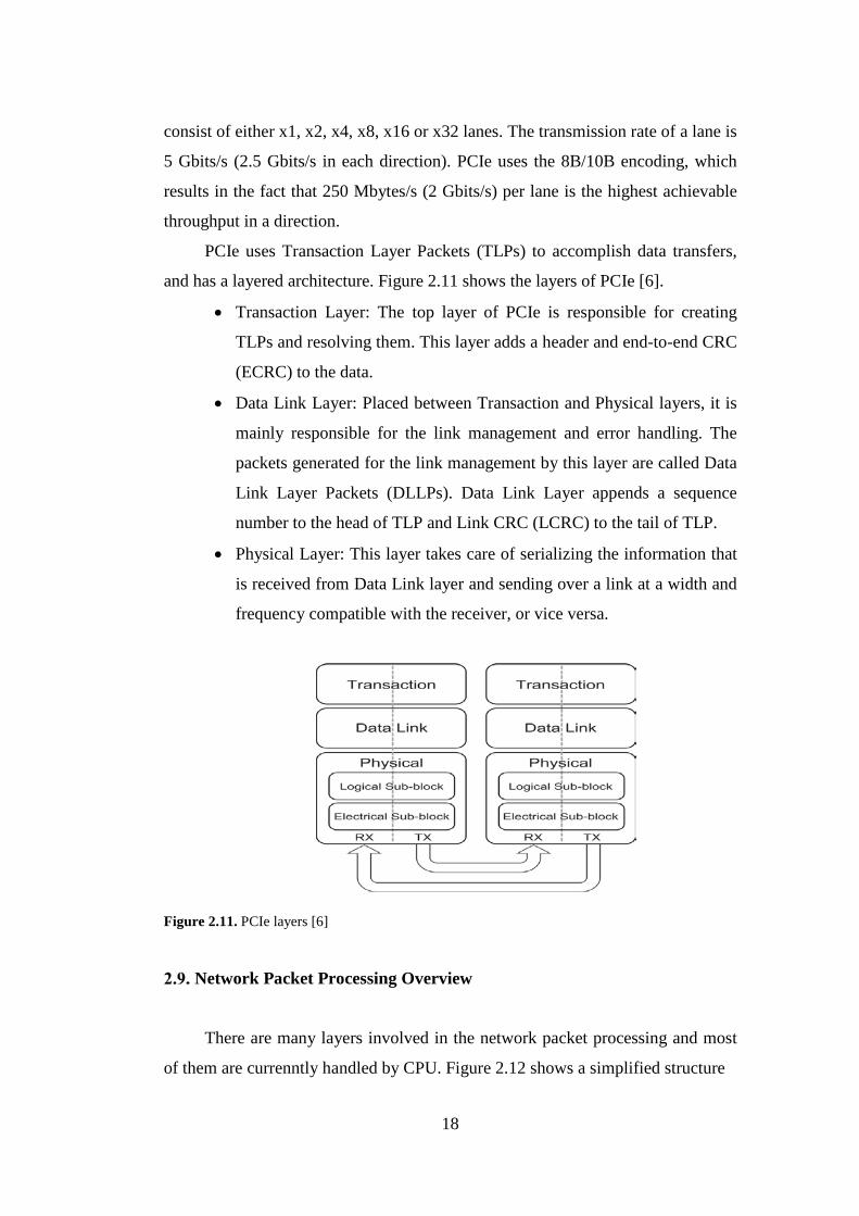
PCIe uses Transaction Layer Packets (TLPs) to accomplish data transfers,
and has a layered architecture. Figure 2.11 shows the layers of PCIe [6].
• Transaction Layer: The top layer of PCIe is responsible for creating
TLPs and resolving them. This layer adds a header and end-to-end CRC
(ECRC) to the data.
• Data Link Layer: Placed between Transaction and Physical layers, it is
mainly responsible for the link management and error handling. The
packets generated for the link management by this layer are called Data
Link Layer Packets (DLLPs). Data Link Layer appends a sequence
number to the head of TLP and Link CRC (LCRC) to the tail of TLP.
• Physical Layer: This layer takes care of serializing the information that
is received from Data Link layer and sending over a link at a width and
frequency compatible with the receiver, or vice versa.
Figure 2.11. PCIe layers [6]
Network Packet Processing Overview
There are many layers involved in the network packet processing and most
of them are currenntly handled by CPU. Figure 2.12 shows a simplified structure
18

Figure 2.12. Operational structure of the network stack [14]
of the packet processing [14], where it is run in three different system mode of
operation, namely user, kernel and device. User and kernel modes together are
called host and device is a Network Interface Card (NIC).
Applications use sockets that are placed in the kernel space to send data. A
socket is equipped with sending and receiving buffers. When an application wants
to send data, it calls a system call which results in a change in the system mode
from user to kernel, and then, data in the user space is copied to the sending buffer
of the related socket in the kernel space. When data is copied to the socket buffer,
a transport layer protocol is called to encapsulate it by the related protocol header.
The same procedure is applied by the network and data link layer protocols as
well. After an Ethernet frame is partially formed, NIC driver is called upon in
order to copy frames from the main memory to the NIC memory. Finally, NIC
adds preamble, CRC and Interframe Gap to every frame and sends them to the
network.
The data receiving process is similar to the data transmitting one. When an
Ethernet frame is received, NIC writes it into its memory. It checks its CRC, and
if it is valid, NIC copies it to the main memory. After copying, NIC sends an
interrupt request to the host operating system (OS). It should be noted here that
nearly 60 packets are processed per interrupt for 10 GbE and 7 packets for 1 GbE
[15]. A driver changes these frames to a form that OS can understand. Ethernet,
network and transport layers process the related header field, respectively, and
19
then, each layer removes it. Finally, the received data is written to the receive
buffer of the socket. When application calls the read system call, data is copied
from the kermel to to user space and removed from the socket buffer.
This network stack processing puts a large amount of load on CPU. In [15],
the core utilization related to the network packet processing for 10 Gbps was
studied. The experiments in [15] showed that two cores of Quad-Core Intel Xeon
5355 processor which are running at 2.66 GHz are saturated in order to reach the
line rate throughput. The amount of core utilization was about 225%.
In addition to [15], the core utilization of network packet processing for 1
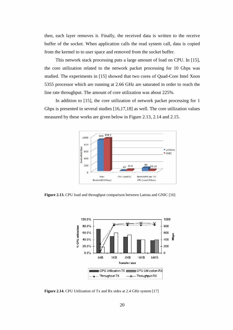
Gbps is presented in several studies [16,17,18] as well. The core utilization values
measured by these works are given below in Figure 2.13, 2.14 and 2.15.
Figure 2.13. CPU load and throughput comparison between Latona and GNIC [16]
Figure 2.14. CPU Utilization of Tx and Rx sides at 2.4 GHz system [17]
20
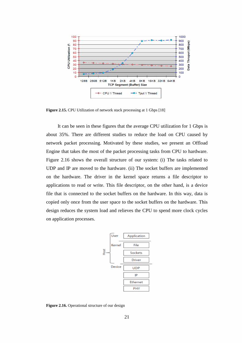
Figure 2.15. CPU Utilization of network stack processing at 1 Gbps [18]
It can be seen in these figures that the average CPU utilization for 1 Gbps is
about 35%. There are different studies to reduce the load on CPU caused by
network packet processing. Motivated by these studies, we present an Offload
Engine that takes the most of the packet processing tasks from CPU to hardware.
Figure 2.16 shows the overall structure of our system: (i) The tasks related to
UDP and IP are moved to the hardware. (ii) The socket buffers are implemented
on the hardware. The driver in the kernel space returns a file descriptor to
applications to read or write. This file descriptor, on the other hand, is a device
file that is connected to the socket buffers on the hardware. In this way, data is
copied only once from the user space to the socket buffers on the hardware. This
design reduces the system load and relieves the CPU to spend more clock cycles
on application processes.
Figure 2.16. Operational structure of our design
21

Related Work
In the literature, there are several examples of design and implementation of
UDP/IP and TCP/IP protocol stacks on hardware. Löfgren et al. [19] presented
three cores as minimum, medium, and advanced for different network system
requirements. All of these three cores are based on the same architecture. The
minimum core is designed mostly for one way network traffic, either send or
receive. Since it is designed for minimal systems, it is very area effective but not
flexible. Medium core is based on the Minimum core implementation. ARP and
ICMP functionalities are included in this design, and it offers higher flexibility
than Minimum. This is a mediocre core between Minimum and Advanced cores.
Advanced core can operate at gigabit speed and can handle packets with the
length of 1518 bytes (1472 bytes of application data). Minimum and Medium
designs can handle packet sizes up to 256 bytes. Additionally, Reverse Address
Resolution Protocol (RARP) is implemented by Advanced core.
In [20], an efficient communication between PC and FPGA is aimed. In
order to minimize the I/O operation for the data transmission between PC-FPGA,
they present a core design. PC and FPGA are connected with an Ethernet cable.
This design contains an Ethernet MAC (EMAC) core for Ethernet connection.
Their design has components that handles transport layer and internet layer
level packets encapsulation and decapsulation processes. UDP and IPv4 protocols
are used for the transport and internet layers. A look up table (LUT) is used for the
static fields of the UDP and IPv4 protocols.
Alachiotis et al. [21] proposed an extended version of their previous work
which takes more area in exchange for a better performance and flexibility. The
main difference is that the static header field is controlled by an initialization
packet from PC. The extended version also offers a communication protocol and
provides a sortware/hardware interface and communication library
implementation for the use of design.
Herrmann et al. [22] present a UDP/IP stack on FPGA. Transport, network
and link layers are implemented on hardware, and UDP, IPv4 and Ethernet
protocols are used for these layers respectively. Different from our work, this
22

study does not use a provided IP core for the ethernet connectivity, and it is based
on its IP component that is designed to handle the MAC layer processes. This
design offers a theoretical 1960 Mbps of full duplex throughput.
Dollas et al. [23] present a TCP/IP stack on FPGA. This is one of the most
comprehensive works in the literature and it implements TCP, UDP, IP, ARP
ICMP protocols. Virtex 2 FPGA is used for the implementation of the system.
Overall design has a 37.5 MHz maximum working frequency and an 8-bit
datapath, so the system can achieve 350 Mbps throughput. TCP is the slowest
component in this design. If TCP is removed and UDP is kept as the only protocol
in the transport layer, the system frequency would go higher and a better
throughput would be achieved.
Vishwanath et al. [24] combine the better sides of TCP and UDP protocols
and offer an emulated UDP Offload Engine (UOE). This design is based on the
Chelsio T110 TCP Offload Engine (TOE) [25], and it implements high
performance UDP/IP sockets for applications to use the design.
In [26], two different versions of a UDP/IP core are presented. The only
difference between two versions is UDP checksum calculation. This core can
operate at gigabit speed and implements UDP, IP and ARP protocols. The core
implementation is realized on Spartan 6 FPGA.
In [27], the socket processing in addition to the TCP/IP processing is
offloaded to the hardware to reduce the system overhead. A software-hardware
codesign on system-on-chip is presented in [28] to improve the performance of
the network protocol processing and provide quality of service functionality for
the real-time applications. This core can operate at 100 Mbps. In [29], ARP
protocol is implemented on Virtex 5 FPGA. In [30], a minimal UDP/IP stack on
FPGA is presented so that it can be used for the real-time transmission of sensor
data in sonar systems. In [31], a 10 G TOE with low latency is proposed, and it is
implemented on several FPGAs such as Virtex 5, Virtex 6, Spartan 6 and Zynq
platforms. In [32], the network stack processing is offloaded to a dedicated
processor core. Only one core deals with the protocol stack tasks and other cores
deal with other system tasks. In [33], a UDP/IP ASIC is used to accelerate
23

multimedia transmission. The design uses jumbo frames to reduce the packet
number and interrupt durations.
24
3. SYSTEM DESIGN
In this chapter, we present the system architecture of the IP core proposed,
introduce a few third party IP components and an API in order for the network
applications to use Offload Engine.
Overall System Architecture
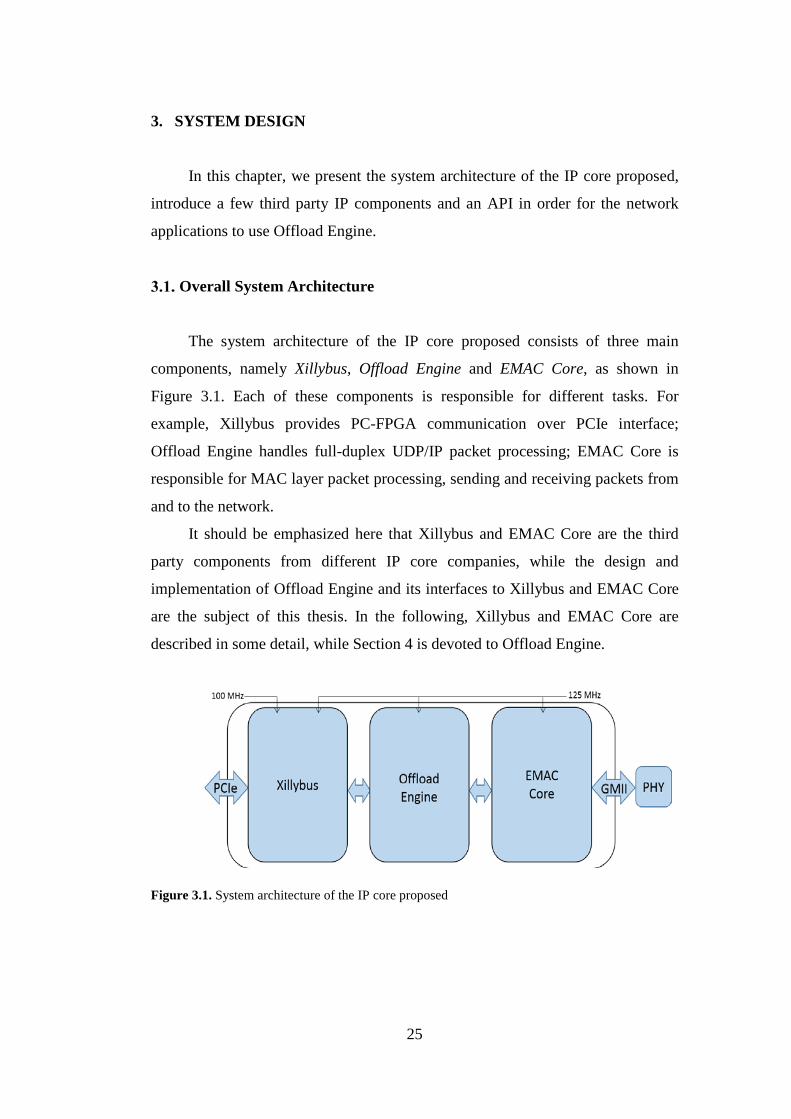
The system architecture of the IP core proposed consists of three main
components, namely Xillybus, Offload Engine and EMAC Core, as shown in
Figure 3.1. Each of these components is responsible for different tasks. For
example, Xillybus provides PC-FPGA communication over PCIe interface;
Offload Engine handles full-duplex UDP/IP packet processing; EMAC Core is
responsible for MAC layer packet processing, sending and receiving packets from
and to the network.
It should be emphasized here that Xillybus and EMAC Core are the third
party components from different IP core companies, while the design and
implementation of Offload Engine and its interfaces to Xillybus and EMAC Core
are the subject of this thesis. In the following, Xillybus and EMAC Core are
described in some detail, while Section 4 is devoted to Offload Engine.
Figure 3.1. System architecture of the IP core proposed
25
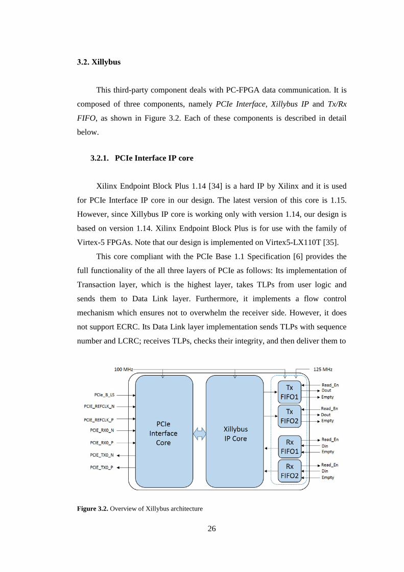
Xillybus
This third-party component deals with PC-FPGA data communication. It is
composed of three components, namely PCIe Interface, Xillybus IP and Tx/Rx
FIFO, as shown in Figure 3.2. Each of these components is described in detail
below.
3.2.1. PCIe Interface IP core
Xilinx Endpoint Block Plus 1.14 [34] is a hard IP by Xilinx and it is used
for PCIe Interface IP core in our design. The latest version of this core is 1.15.
However, since Xillybus IP core is working only with version 1.14, our design is
based on version 1.14. Xilinx Endpoint Block Plus is for use with the family of
Virtex-5 FPGAs. Note that our design is implemented on Virtex5-LX110T [35].
This core compliant with the PCIe Base 1.1 Specification [6] provides the
full functionality of the all three layers of PCIe as follows: Its implementation of
Transaction layer, which is the highest layer, takes TLPs from user logic and
sends them to Data Link layer. Furthermore, it implements a flow control
mechanism which ensures not to overwhelm the receiver side. However, it does
not support ECRC. Its Data Link layer implementation sends TLPs with sequence
number and LCRC; receives TLPs, checks their integrity, and then deliver them to
Figure 3.2. Overview of Xillybus architecture
26
Transaction layer. It can also handle error detection and correction, and request
retransmissions for the corrupted packets. Its Physical layer implementation is
responsible for transmitting, receiving the packets to and from the link.
There are seven signals for PCIe Interface core in Figure 3.2: PCIe_B_LS is
a reset signal, PCIE_REFCLK_N and PCIE_REFCLK_P are 100 MHz
differential clock signals. Other four differential signals are used for the data
communication, where TX and RX are for transmitting and receiving, respectively.
3.2.2. Xillybus IP core
Xilinx Endpoint Block Plus alone is too primitve in nature to harness the
power of PCIe interface immediately. Consequently, a user must still encode or
decode data to form packets while obeying the many rules of the PCIe
specification for addressing, packet size, etc. [6]. Once packets have been created,
there are still several design hurdles and a great deal of effort that must be spent in
order to turn these primitive interfaces into a useful one. Fortunetely, Xillybus
[36] provides a soft IP core that offers an immediate solution to the adoption of
PCIe interface in custom designs.
Xillybus provides host-FPGA data communication over PCIe interface,
where it uses simple FIFO interfaces for the communication with user logic on
FPGA and basic file descriptors for the interaction with user applications running
on host. Furthermore, this IP core can be built with the selected features such as
channel count, channel width and maximum throughput through Xillybus IP
factory from Xillybus web page [37].
Xillybus works with a 100 MHz clock and the rest of the system must be
designed according to this. Xillybus has three different data widths as 8 bits, 16
bits and 32 bits. Higher data widths allow higher performance. However, Xillybus
does not guarantee a continuous data flow, and there may be gaps between data
blocks in any time during the data transmission. In our design, a Xillybus IP core
with 32-bit send and receive interfaces is used for achieving 1 Gbit/s data
throughput. Furthermore, as shown in Figure 3.2, Xillybus has two read (Rx
FIFO) and two write (Tx FIFO) interfaces. Beside these interfaces, it has also a
27

memory interface for the configuration of Offload Engine, which is not shown in
Figure 3.2.
3.2.3. Xilinx FIFOs
Offload Engine provides two independent transmission channels in each
direction. As a result, two different applications running on a host can send and
receive data at the same time. Since there are two channels, Xillybus must be
interfaced with two Tx FIFOs and two Rx FIFOs as shown in Figure 3.2.
Tx and Rx FIFOs in Figure 3.2 are 2 Kbyte buffers generated using Xilinx
FIFO generator IP core, where Tx FIFOs are wrapped with a First Word Fall
Through (FWFT) wrapper and Rx FIFOs, on the other hand, are standard ones.
Since Xillybus works with 100 MHz and the rest of the system is designed to use
a 125 MHz clock signal, these FIFOs are chosen to have independent read and
write clock signals so as to alleviate clock domain crossing problems.
Furthermore, FIFOs provide data width conversion as well, where Xillybus-FIFO
data bus interface is 32-bit, while Offload Engine-FIFO one is 8-bit.
With respect to Figure 3.2, a standard or FWFT FIFO has three signals in
each side: Write Enable, Data Input and Full signals are available for the write
interface, while Read Enable (Read_En), Data Output (Dout) and Empty signals
are present for the read interface. It should be noted here that the difference
between a standard FIFO and FWFT FIFO is only about reading data from FIFO.
Standard FIFOs have a read latency of one clock cycle, whereas FWFT FIFOs can
provide data in the same clock cycle in which Read_En is asserted.
MAC IP Core
MAC IP core [38] is from Xilinx and it is responsible for MAC layer
encapsulation, sending and receiving packets to and from the network over the
PHY chip on the board. MAC IP core has three components: Tx/Rx FIFOs,
EMAC core and GMII physical interface. Figure 3.3 shows the architecture of
MAC IP core.
28
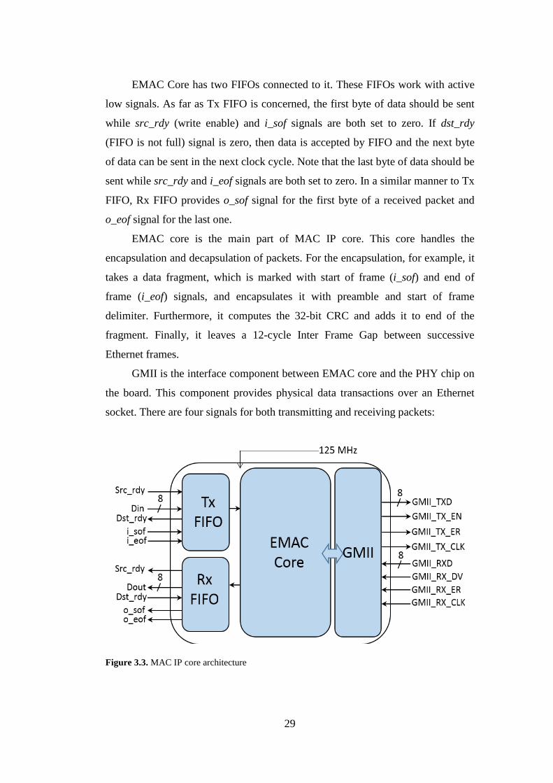
EMAC Core has two FIFOs connected to it. These FIFOs work with active
low signals. As far as Tx FIFO is concerned, the first byte of data should be sent
while src_rdy (write enable) and i_sof signals are both set to zero. If dst_rdy
(FIFO is not full) signal is zero, then data is accepted by FIFO and the next byte
of data can be sent in the next clock cycle. Note that the last byte of data should be
sent while src_rdy and i_eof signals are both set to zero. In a similar manner to Tx
FIFO, Rx FIFO provides o_sof signal for the first byte of a received packet and
o_eof signal for the last one.
EMAC core is the main part of MAC IP core. This core handles the
encapsulation and decapsulation of packets. For the encapsulation, for example, it
takes a data fragment, which is marked with start of frame (i_sof) and end of
frame (i_eof) signals, and encapsulates it with preamble and start of frame
delimiter. Furthermore, it computes the 32-bit CRC and adds it to end of the
fragment. Finally, it leaves a 12-cycle Inter Frame Gap between successive
Ethernet frames.
GMII is the interface component between EMAC core and the PHY chip on
the board. This component provides physical data transactions over an Ethernet
socket. There are four signals for both transmitting and receiving packets:
Figure 3.3. MAC IP core architecture
29
GMII_TXD is 8-bit data out bus. When the data on GMII_TXD is valid,
GMII_TX_EN is set to 1. GMII_TX_ER is used for error cases. GMII_TX_CLK
is used for the synchronization of data on the receiver. The receiver signals are
basically the counterparts of these transmit signals.
It should be emphasized that the sender and receiver functionalities of MAC
IP core are mostly independent and the IP can work in full-duplex mode. Since the
IP is designed for gigabit speed communication, 2 Gbit/s is the theoretically
achievable throughput in full-duplex mode.
3.4. Custom FIFOs
In addition to Xilinx FIFOs used by Xillybus, the design of Offload Engine
relies on custom FWFT FIFO buffers as well. These FWFT FIFOs in Offload
Engine are generated by means of a generic FWFT FIFO design, which is
configurable according to its width and depth parameters, developed within the
scope of the thesis. Furthermore, their write and read interfaces are similar to
Xilinx FIFOs.
In Offload Engine, all components except for the ICMP use two-entry,
custom design FWFT FIFOs. ICMP has an extra 128-entry FWFT FIFO for
saving the data in a ping request.
3.5. API for Offload Engine
An application programming interface (API) is designed for applications
running on a host to exploit Offload Engine. This API has 4 different functions:
udp_offload_send, udp_offload_receive, udp_offload_config and
udp_offload_socket. Each of these functions have a udp_offload prefix to prevent
mixing these functions with sendto and recvfrom functions that are normally used
for sending and receiving data using network protocols available in the operating
system. Applications can send data to FPGA and receive data from it using these
API functions. These functions are explained in detail below.
30
• udp_offload_socket (int pnum): This function returns an integer that
represents the socket number to application. Application then can send
and receive data using this socket number. Application can select the
source port number by specifying pnum parameter. If the parameter is not
used, then API assigns a random source port number for the socket.
• udp_offload_send (int snum, int dip, int port, int len, const char *buf):
This is used for sending data to FPGA and takes five parameters: socket
number (snum), destination IP address (dip), destination port number
(port), data length in bytes (len) and character pointer to data (*buf)
respectively. Note that API zero-extends 16-bit destination port number
to 32-bit so that 32-bit Xillybus driver can be used by default.
• udp_offload_receive (int snum, int len, char *buf): This function takes
three parameters and is used for receiving data from FPGA. When
application calls this function and if there is received data in FPGA, API
writes the data to the given buffer parameter and returns the amount of
the written data.
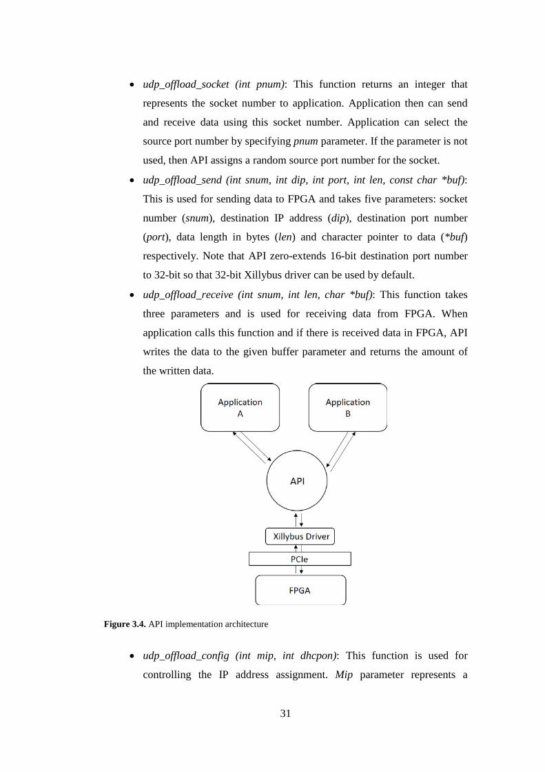
Figure 3.4. API implementation architecture
• udp_offload_config (int mip, int dhcpon): This function is used for
controlling the IP address assignment. Mip parameter represents a
31
manual IP address that is given by a user. Dhcpon parameter activates or
deactivates the DHCP component in Offload Engine.
Figure 3.4 shows how this API helps applications to use Offload Engine.
Applications send and receive data using the aferomentioned API functions. Once
an application calls udp_offload_send API function to send data, API writes the
data to the device file created by the Xillybus driver. Then, the driver copies the
device file to FPGA over PCIe channel. When FPGA sends data to host, it is
taken by the Xillybus device file and the API reads the data from this device file,
then delivers it to the appropriate application.
32

4. OFFLOAD ENGINE
Offload Engine is the IP core that has been fully designed and implemented
in this thesis. The architecture of Offload Engine is given in Figure 4.1, where it
comprises ten different components. All of these components except for
Configuration have a similar architecture and they consist of a Finite State
Machine with Datapath (FSMD) [39] and a FWFT FIFO. Furthermore, these they
all have sender side (Tx) and receiver side (Rx).
Channel Selector, Configuration and UDP Rx components are connected to
Xillybus, whereas Arbitrator, ARP and IP Rx components are interfaced with
MAC IP core. As far as the connection between two Offload Engine components
is concerned, they all expect FWFT FIFO behavior for a seamless integration.
Implemented protocols can be different depending on the purpose of the
design. Our design includes UDP, IP, ARP, ICMP and DHCP protocols.
Compared to the similar works in the literature, DHCP protocol has not been
implemented in any of the previous designs. The implemented protocols in our
design and related works are given in Table 4.1.
Figure 4.1. Offload Engine architecture
33
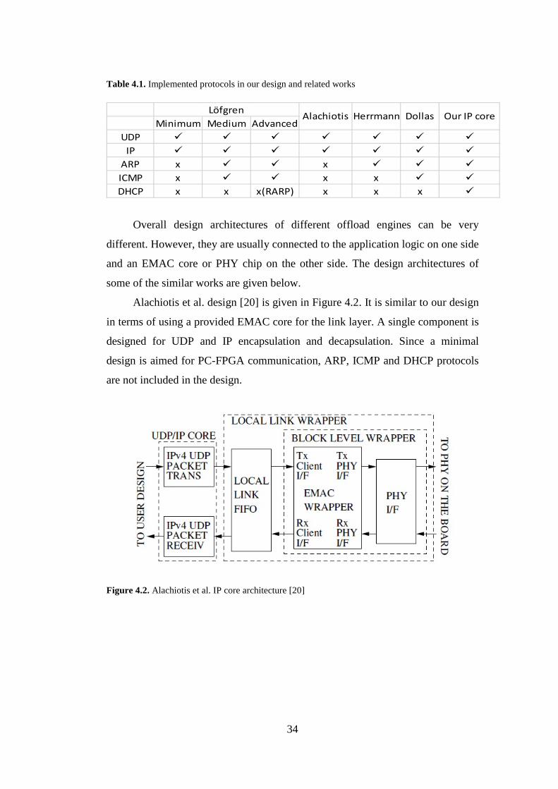
Table 4.1. Implemented protocols in our design and related works
Minimum Medium AdvancedUDP
IP ARP x x ICMP x x x DHCP x x x(RARP) x x x
Löfgren Alachiotis Herrmann Dollas Our IP core
Overall design architectures of different offload engines can be very
different. However, they are usually connected to the application logic on one side
and an EMAC core or PHY chip on the other side. The design architectures of
some of the similar works are given below.
Alachiotis et al. design [20] is given in Figure 4.2. It is similar to our design
in terms of using a provided EMAC core for the link layer. A single component is
designed for UDP and IP encapsulation and decapsulation. Since a minimal
design is aimed for PC-FPGA communication, ARP, ICMP and DHCP protocols
are not included in the design.
Figure 4.2. Alachiotis et al. IP core architecture [20]
34
Figure 4.3. Löfgren et al. IP core architecture [19]
Figure 4.4. Herrmann et al. IP core architecture [22]
35

Löfgren et al. design [19] is given in Figure 4.3. They used the same
architecture for all of the three cores in [9]. This design, different from ours, does
not include a provided EMAC core, instead four components as Transmitter,
Receiver, CRC Generator and CRC Checker does the link layer processes. The
Advanced core includes UDP, IP, ARP, ICMP and RARP protocols.
Herrmann et al. design [22] is given in Figure 4.4. This design is very
similar to [9] in terms of its overall design. This one neither includes a provided
EMAC core nor ICMP and DHCP protocols. The design, however, implements
ARP protocol.
Channel Selector
Channel Selector is the first component in the Tx path of Offload Engine,
and it is employed to select one of the two channels connected to it. The
architecture of Channel Selector is given in Figure 4.5, in which the main
components are 8-bit two entry FIFO buffer and a finite state machine (FSM). The
FSM whose state diagram is given in Figure 4.6 controls the operation of Channel
Selector as follows:
Figure 4.5. Channel Selector architecture
36
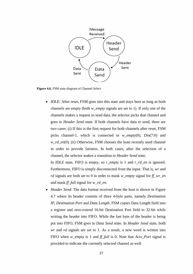
Figure 4.6. FSM state diagram of Channel Select
• IDLE: After reset, FSM goes into this state and stays here as long as both
channels are empty (both w_empty signals are set to 1). If only one of the
channels makes a request to send data, the selector picks that channel and
goes to Header Send state. If both channels have data to send, there are
two cases: (i) If this is the first request for both channels after reset, FSM
picks channel-1, which is connected to w_empty(0), Din(7:0) and
w_rd_en(0). (ii) Otherwise, FSM chooses the least recently used channel
in order to provide fairness. In both cases, after the selection of a
channel, the selector makes a transition to Header Send state.
In IDLE state, FIFO is empty, so r_empty is 1 and r_rd_en is ignored.
Furthermore, FIFO is simply disconnected from the input. That is, wr and
rd signals are both set to 0 in order to mask w_empty signal for ff_wr_en
and mask ff_full signal for w_rd_en.
• Header Send: The data format received from the host is shown in Figure
4.7 where its header consists of three 4-byte parts, namely Destination
IP, Destination Port and Data Length. FSM copies Data Length field into
a register and zero-extend 16-bit Destination Port field to 32-bit while
writing the header into FIFO. While the last byte of the header is being
put into FIFO, FSM goes to Data Send state. In Header Send state, both
wr and rd signals are set to 1. As a result, a new word is written into
FIFO when w_empty is 1 and ff_full is 0. Note that Actv_Port signal is
provided to indicate the currently selected channel as well.
37

Figure 4.7. Host data format
• Data Send: FSM counts the number of data bytes that are put into FIFO
by a counter, waits for the counter to reach Data Length value kept in the
register, and then, makes a transition to IDLE state. Note that data may
come in an on-and-off fashion, which will be nicely handled by FSM.
According to the aferomentioned FSM operation, it takes at least N+13
clock cycles to write header and N-byte of data into FIFO. After the first word is
written into FIFO, it will take N+12 clock cycles to read them.
UDP Tx
UDP Tx component is the sender implemetation of UDP protocol, and its
architecure is given in Figure 4.8. According to Figure 4.8, two different
components, namely Channel Selector or DHCP IP core, can be a source of data.
As a result, UDP Tx is responsible for encapsulating the data that are received
from either Channel Selector or DHCP IP core with UDP header and sending
UDP datagrams to IP Tx component. Note that DHCP IP core has the priority
over Channel Selector in our design and these two components are not usually
active at the same time.
UDP Tx further relies on Configuration IP to provide a UDP source port
number related to the chosen channel by Channel Selector. Thus, Configuration IP
provides two 16-bit UDP source port numbers, each of which is exclusively
assigned to a channel, through 32-bit Cfg_Ports signal. According to Actv_Port
signal coming from Channel Selector, UDP Tx inserts the correct source port
number into UDP datagrams. For DHCP packets, however, the source port
number is fixed at Hexadecimal 0044 and it is chosen by setting src_sel signal to
one.
38
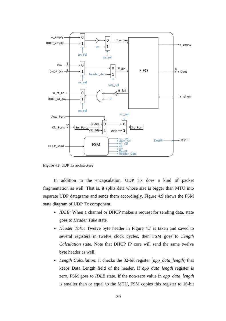
Figure 4.8. UDP Tx architecture
In addition to the encapsulation, UDP Tx does a kind of packet
fragmentation as well. That is, it splits data whose size is bigger than MTU into
separate UDP datagrams and sends them accordingly. Figure 4.9 shows the FSM
state diagram of UDP Tx component.
• IDLE: When a channel or DHCP makes a request for sending data, state
goes to Header Take state.
• Header Take: Twelve byte header in Figure 4.7 is taken and saved to
several registers in twelve clock cycles, then FSM goes to Length
Calculation state. Note that DHCP IP core will send the same twelve
byte header as well.
• Length Calculation: It checks the 32-bit register (app_data_length) that
keeps Data Length field of the header. If app_data_length register is
zero, FSM goes to IDLE state. If the non-zero value in app_data_length
is smaller than or equal to the MTU, FSM copies this register to 16-bit
39
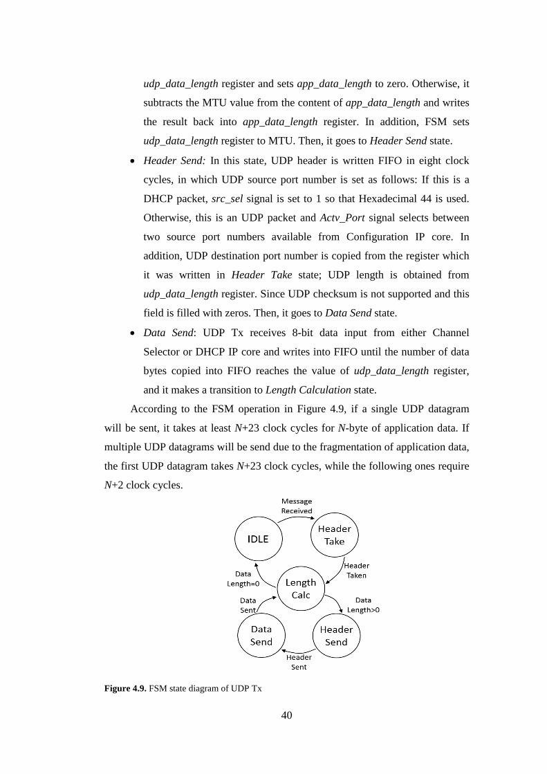
udp_data_length register and sets app_data_length to zero. Otherwise, it
subtracts the MTU value from the content of app_data_length and writes
the result back into app_data_length register. In addition, FSM sets
udp_data_length register to MTU. Then, it goes to Header Send state.
• Header Send: In this state, UDP header is written FIFO in eight clock
cycles, in which UDP source port number is set as follows: If this is a
DHCP packet, src_sel signal is set to 1 so that Hexadecimal 44 is used.
Otherwise, this is an UDP packet and Actv_Port signal selects between
two source port numbers available from Configuration IP core. In
addition, UDP destination port number is copied from the register which
it was written in Header Take state; UDP length is obtained from
udp_data_length register. Since UDP checksum is not supported and this
field is filled with zeros. Then, it goes to Data Send state.
• Data Send: UDP Tx receives 8-bit data input from either Channel
Selector or DHCP IP core and writes into FIFO until the number of data
bytes copied into FIFO reaches the value of udp_data_length register,
and it makes a transition to Length Calculation state.
According to the FSM operation in Figure 4.9, if a single UDP datagram
will be sent, it takes at least N+23 clock cycles for N-byte of application data. If
multiple UDP datagrams will be send due to the fragmentation of application data,
the first UDP datagram takes N+23 clock cycles, while the following ones require
N+2 clock cycles.
Figure 4.9. FSM state diagram of UDP Tx
40
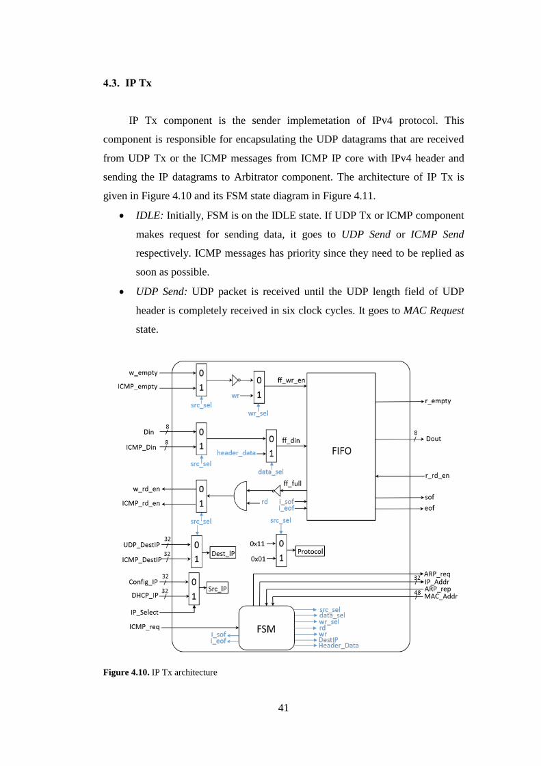
IP Tx
IP Tx component is the sender implemetation of IPv4 protocol. This
component is responsible for encapsulating the UDP datagrams that are received
from UDP Tx or the ICMP messages from ICMP IP core with IPv4 header and
sending the IP datagrams to Arbitrator component. The architecture of IP Tx is
given in Figure 4.10 and its FSM state diagram in Figure 4.11.
• IDLE: Initially, FSM is on the IDLE state. If UDP Tx or ICMP component
makes request for sending data, it goes to UDP Send or ICMP Send
respectively. ICMP messages has priority since they need to be replied as
soon as possible.
• UDP Send: UDP packet is received until the UDP length field of UDP
header is completely received in six clock cycles. It goes to MAC Request
state.
Figure 4.10. IP Tx architecture
41
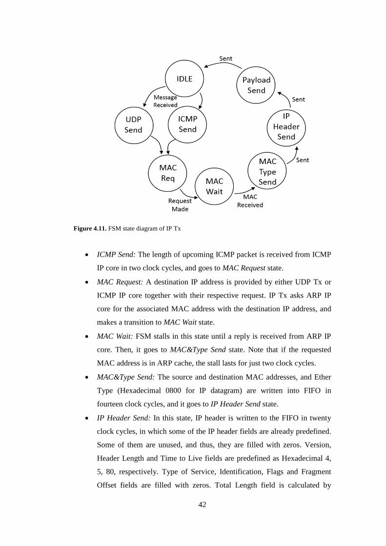
Figure 4.11. FSM state diagram of IP Tx
• ICMP Send: The length of upcoming ICMP packet is received from ICMP
IP core in two clock cycles, and goes to MAC Request state.
• MAC Request: A destination IP address is provided by either UDP Tx or
ICMP IP core together with their respective request. IP Tx asks ARP IP
core for the associated MAC address with the destination IP address, and
makes a transition to MAC Wait state.
• MAC Wait: FSM stalls in this state until a reply is received from ARP IP
core. Then, it goes to MAC&Type Send state. Note that if the requested
MAC address is in ARP cache, the stall lasts for just two clock cycles.
• MAC&Type Send: The source and destination MAC addresses, and Ether
Type (Hexadecimal 0800 for IP datagram) are written into FIFO in
fourteen clock cycles, and it goes to IP Header Send state.
• IP Header Send: In this state, IP header is written to the FIFO in twenty
clock cycles, in which some of the IP header fields are already predefined.
Some of them are unused, and thus, they are filled with zeros. Version,
Header Length and Time to Live fields are predefined as Hexadecimal 4,
5, 80, respectively. Type of Service, Identification, Flags and Fragment
Offset fields are filled with zeros. Total Length field is calculated by
42
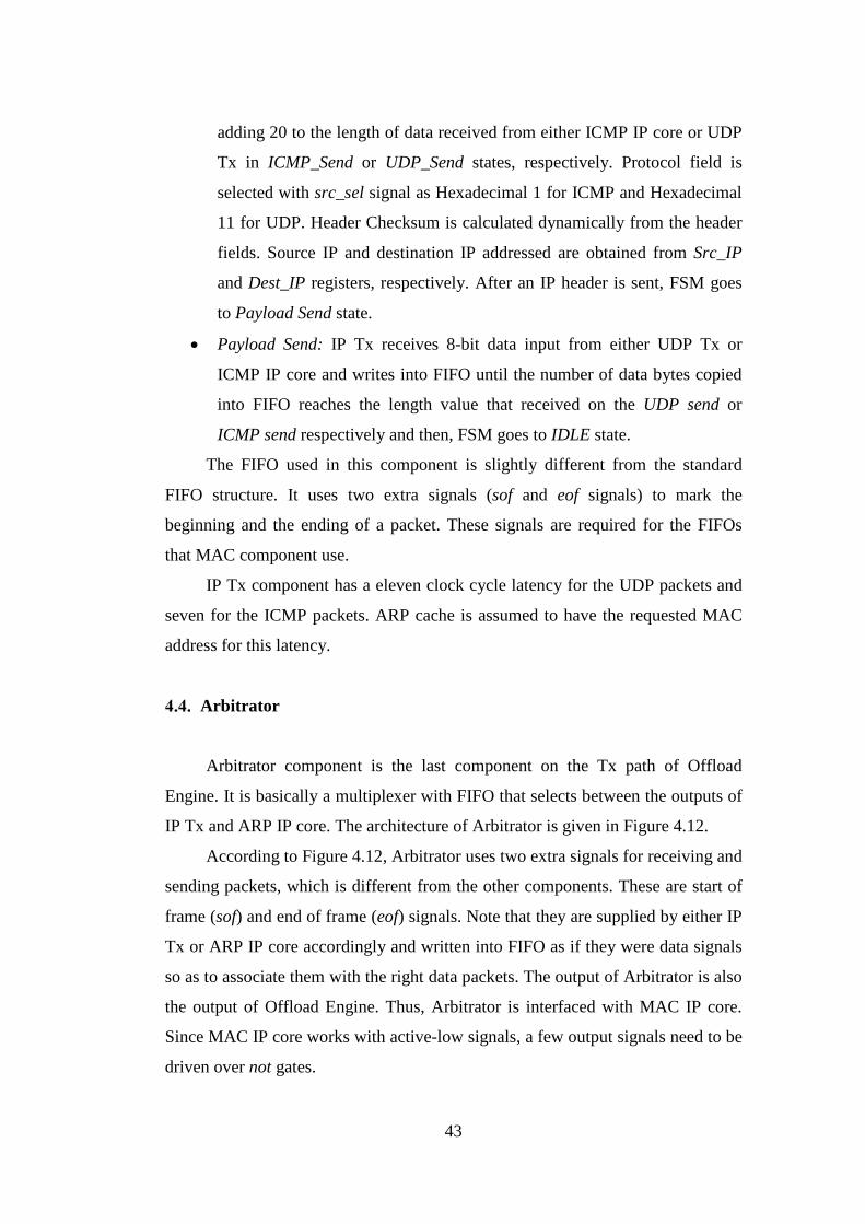
adding 20 to the length of data received from either ICMP IP core or UDP
Tx in ICMP_Send or UDP_Send states, respectively. Protocol field is
selected with src_sel signal as Hexadecimal 1 for ICMP and Hexadecimal
11 for UDP. Header Checksum is calculated dynamically from the header
fields. Source IP and destination IP addressed are obtained from Src_IP
and Dest_IP registers, respectively. After an IP header is sent, FSM goes
to Payload Send state.
• Payload Send: IP Tx receives 8-bit data input from either UDP Tx or
ICMP IP core and writes into FIFO until the number of data bytes copied
into FIFO reaches the length value that received on the UDP send or
ICMP send respectively and then, FSM goes to IDLE state.
The FIFO used in this component is slightly different from the standard
FIFO structure. It uses two extra signals (sof and eof signals) to mark the
beginning and the ending of a packet. These signals are required for the FIFOs
that MAC component use.
IP Tx component has a eleven clock cycle latency for the UDP packets and
seven for the ICMP packets. ARP cache is assumed to have the requested MAC
address for this latency.
Arbitrator
Arbitrator component is the last component on the Tx path of Offload
Engine. It is basically a multiplexer with FIFO that selects between the outputs of
IP Tx and ARP IP core. The architecture of Arbitrator is given in Figure 4.12.
According to Figure 4.12, Arbitrator uses two extra signals for receiving and
sending packets, which is different from the other components. These are start of
frame (sof) and end of frame (eof) signals. Note that they are supplied by either IP
Tx or ARP IP core accordingly and written into FIFO as if they were data signals
so as to associate them with the right data packets. The output of Arbitrator is also
the output of Offload Engine. Thus, Arbitrator is interfaced with MAC IP core.
Since MAC IP core works with active-low signals, a few output signals need to be
driven over not gates.
43
Figure 4.12. Arbitrator architecture
There is no need to draw a FSM state diagram for Arbitrator, since it
consist of only two states as IDLE and SEND. Arbitrator waits in IDLE state.
When IP Tx or ARP IP makes a request, it goes to SEND state, where it stays until
the end of packet that will be marked by an end of frame signal. Then, it return to
IDLE state.
Arbitrator has a two clock cycle latency. The total latency on the Tx path for
an N-byte of application data is N+40 (12 clock cycles for application header + 28
clock cycles for Offload Engine) clock cycles.
IP Rx
IP Rx is the first component on the Rx path of Offload Engine. It accepts
only those IP packets that are addressed to this host, and drops any multicast and
broadcast packets. Furthermore, it delivers a received packet to either UDP Rx or
ICMP IP core. Figure 4.13 shows the architecture of IP Rx component. Note that
IP RX does not include a FIFO buffer, and it is basically an FSM together with a
44

couple of multiplexers and demultiplexers. This component has a simple FSM
with five states as shown in Figure 4.14.
• IDLE: When a new packet is received, MAC IP core starts to deliver it to
Offload Engine. IP Rx is the first component to process a newly arriving
packet. So, FSM goes to MAC Type In state to handle a new packet.
• MAC Type In: The destination and source MAC address fields are
ignored, but Ether Type field in the received Ethernet frame is checked.
If this field is equal to Hexadecimal 0800 (IP datagram), the packet is
accepted. Otherwise, it is dropped.
• IP Header In: It checks some of the IP header fields: Protocol, Flags and
Destination IP address. After checking theese fields, if the packet is
approved, it is delivered either UDP Rx or ICMP IP core depending on
Protocol field in the IP header, and FSM goes to Deliver Packet state. If
it is disapproved, FSM goes to Drop state.
Figure 4.13. IP Rx architecture
45

Figure 4.14. FSM state diagram of IP Rx
• Deliver Packet: The received ICMP or UDP packet is delivered to the
related component. Once it is compeletly received, FSM goes to IDLE
state.
• Drop: FSM stays in this state until the packet is fully received, and then
it goes to IDLE state.
UDP Rx
UDP Rx component is the second and the last component on the Rx path of
Offload Engine. It is responsible for receiving the UDP datagrams from IP Rx and
delivering them to either appropriate channel (channel demultiplexing) or DHCP
IP core. Furthermore, UDP Rx drops those packets that are not addressed to one
of its UDP source ports. Figure 4.15 shows architecture of UDP Rx component.
Similar to IP Rx, UDP Rx is composed of an FSM and several multiplexers
and demultiplexers. The FSM of UDP Rx is shown in Figure 4.16. FSM checks
the Destination Port field of the UDP header and if the packet is addressed to
DHCP or one of the applications running on the host, it delivers the packet to
DHCP or Xillybus component respectively.
46
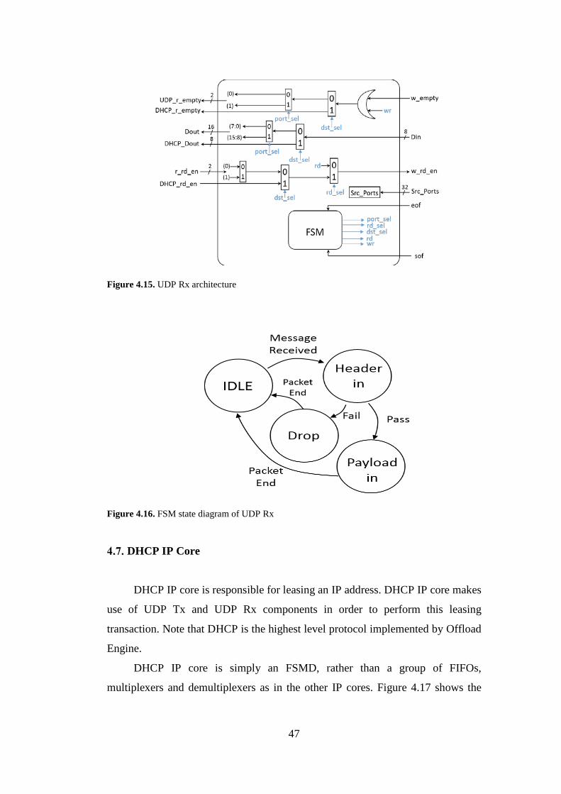
Figure 4.15. UDP Rx architecture
Figure 4.16. FSM state diagram of UDP Rx
DHCP IP Core
DHCP IP core is responsible for leasing an IP address. DHCP IP core makes
use of UDP Tx and UDP Rx components in order to perform this leasing
transaction. Note that DHCP is the highest level protocol implemented by Offload
Engine.
DHCP IP core is simply an FSMD, rather than a group of FIFOs,
multiplexers and demultiplexers as in the other IP cores. Figure 4.17 shows the
47
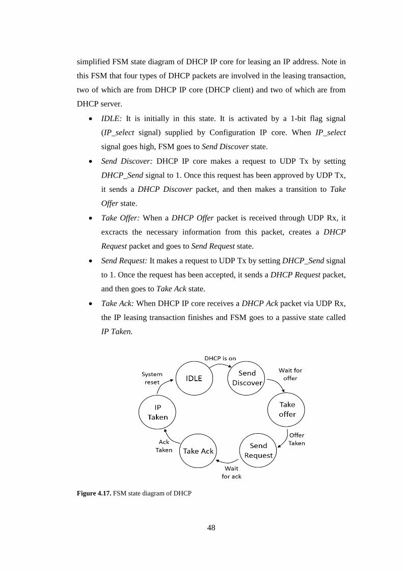
simplified FSM state diagram of DHCP IP core for leasing an IP address. Note in
this FSM that four types of DHCP packets are involved in the leasing transaction,
two of which are from DHCP IP core (DHCP client) and two of which are from
DHCP server.
• IDLE: It is initially in this state. It is activated by a 1-bit flag signal
(IP_select signal) supplied by Configuration IP core. When IP_select
signal goes high, FSM goes to Send Discover state.
• Send Discover: DHCP IP core makes a request to UDP Tx by setting
DHCP_Send signal to 1. Once this request has been approved by UDP Tx,
it sends a DHCP Discover packet, and then makes a transition to Take
Offer state.
• Take Offer: When a DHCP Offer packet is received through UDP Rx, it
excracts the necessary information from this packet, creates a DHCP
Request packet and goes to Send Request state.
• Send Request: It makes a request to UDP Tx by setting DHCP_Send signal
to 1. Once the request has been accepted, it sends a DHCP Request packet,
and then goes to Take Ack state.
• Take Ack: When DHCP IP core receives a DHCP Ack packet via UDP Rx,
the IP leasing transaction finishes and FSM goes to a passive state called
IP Taken.
Figure 4.17. FSM state diagram of DHCP
48
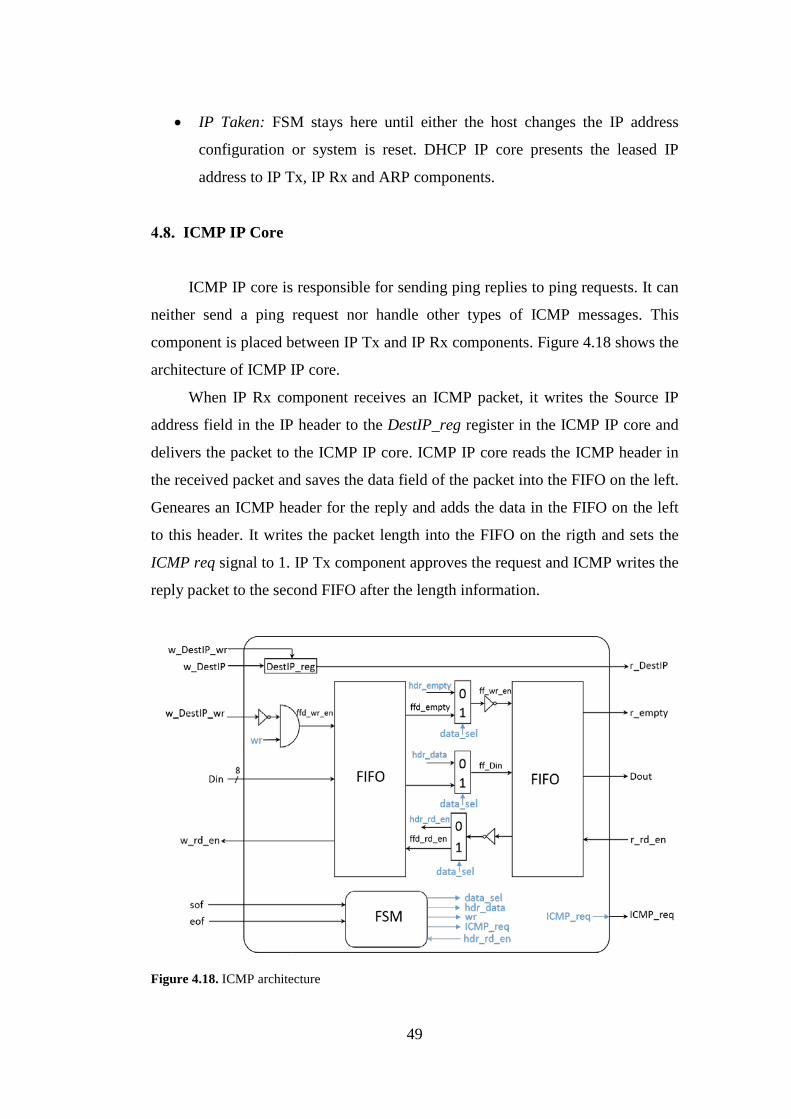
• IP Taken: FSM stays here until either the host changes the IP address
configuration or system is reset. DHCP IP core presents the leased IP
address to IP Tx, IP Rx and ARP components.
ICMP IP Core
ICMP IP core is responsible for sending ping replies to ping requests. It can
neither send a ping request nor handle other types of ICMP messages. This
component is placed between IP Tx and IP Rx components. Figure 4.18 shows the
architecture of ICMP IP core.
When IP Rx component receives an ICMP packet, it writes the Source IP
address field in the IP header to the DestIP_reg register in the ICMP IP core and
delivers the packet to the ICMP IP core. ICMP IP core reads the ICMP header in
the received packet and saves the data field of the packet into the FIFO on the left.
Geneares an ICMP header for the reply and adds the data in the FIFO on the left
to this header. It writes the packet length into the FIFO on the rigth and sets the
ICMP req signal to 1. IP Tx component approves the request and ICMP writes the
reply packet to the second FIFO after the length information.
Figure 4.18. ICMP architecture
49
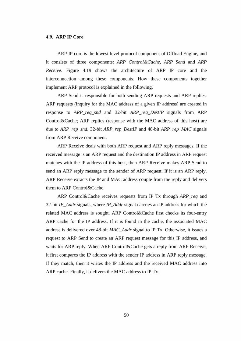
ARP IP Core
ARP IP core is the lowest level protocol component of Offload Engine, and
it consists of three components: ARP Control&Cache, ARP Send and ARP
Receive. Figure 4.19 shows the architecture of ARP IP core and the
interconnection among these components. How these components together
implement ARP protocol is explained in the following.
ARP Send is responsible for both sending ARP requests and ARP replies.
ARP requests (inquiry for the MAC address of a given IP address) are created in
response to ARP_req_snd and 32-bit ARP_req_DestIP signals from ARP
Control&Cache; ARP replies (response with the MAC address of this host) are
due to ARP_rep_snd, 32-bit ARP_rep_DestIP and 48-bit ARP_rep_MAC signals
from ARP Receive component.
ARP Receive deals with both ARP request and ARP reply messages. If the
received message is an ARP request and the destination IP address in ARP request
matches with the IP address of this host, then ARP Receive makes ARP Send to
send an ARP reply message to the sender of ARP request. If it is an ARP reply,
ARP Receive exracts the IP and MAC address couple from the reply and delivers
them to ARP Control&Cache.
ARP Control&Cache receives requests from IP Tx through ARP_req and
32-bit IP_Addr signals, where IP_Addr signal carrries an IP address for which the
related MAC address is sought. ARP Control&Cache first checks its four-entry
ARP cache for the IP address. If it is found in the cache, the associated MAC
address is delivered over 48-bit MAC_Addr signal to IP Tx. Otherwise, it issues a
request to ARP Send to create an ARP request message for this IP address, and
waits for ARP reply. When ARP Control&Cache gets a reply from ARP Receive,
it first compares the IP address with the sender IP address in ARP reply message.
If they match, then it writes the IP address and the received MAC address into
ARP cache. Finally, it delivers the MAC address to IP Tx.
50
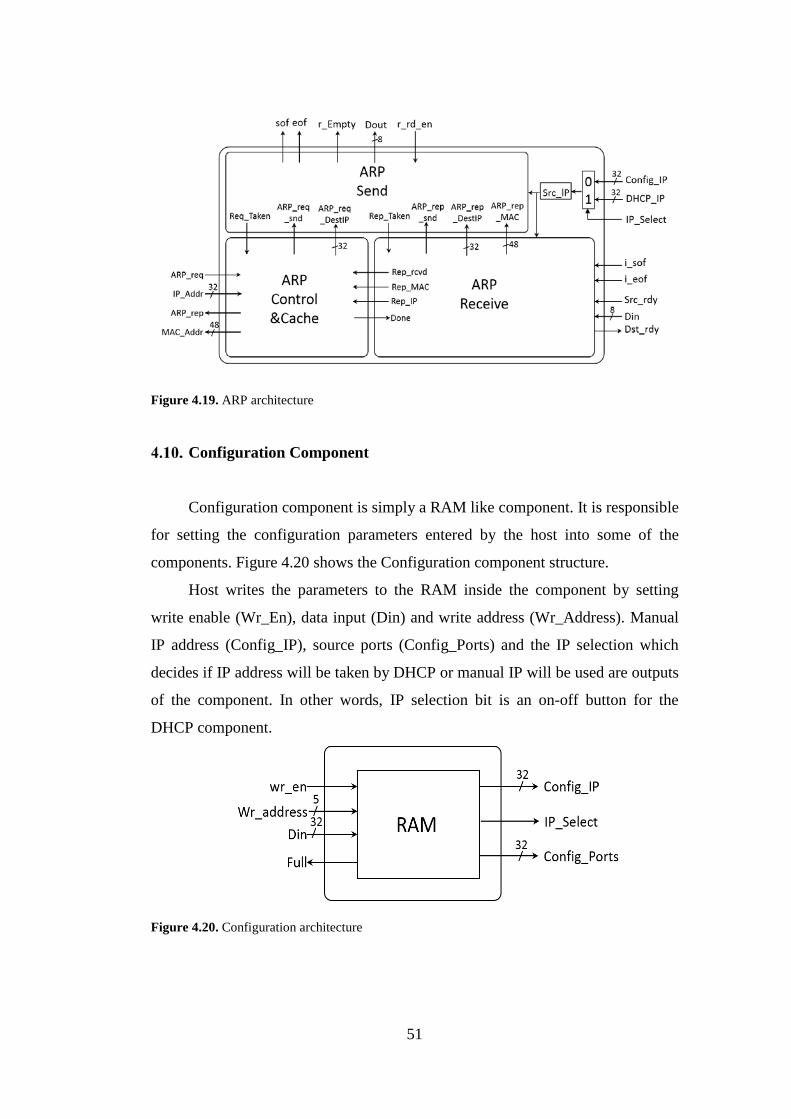
Figure 4.19. ARP architecture
Configuration Component
Configuration component is simply a RAM like component. It is responsible
for setting the configuration parameters entered by the host into some of the
components. Figure 4.20 shows the Configuration component structure.
Host writes the parameters to the RAM inside the component by setting
write enable (Wr_En), data input (Din) and write address (Wr_Address). Manual
IP address (Config_IP), source ports (Config_Ports) and the IP selection which
decides if IP address will be taken by DHCP or manual IP will be used are outputs
of the component. In other words, IP selection bit is an on-off button for the
DHCP component.
Figure 4.20. Configuration architecture
51
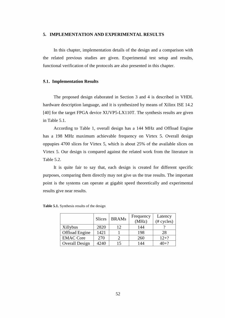
5. IMPLEMENTATION AND EXPERIMENTAL RESULTS
In this chapter, implementation details of the design and a comparison with
the related previous studies are given. Experimental test setup and results,
functional verification of the protocols are also presented in this chapter.
Implementation Results
The proposed design elaborated in Section 3 and 4 is described in VHDL
hardware description language, and it is synthesized by means of Xilinx ISE 14.2
[40] for the target FPGA device XUVP5-LX110T. The synthesis results are given
in Table 5.1.
According to Table 1, overall design has a 144 MHz and Offload Engine
has a 198 MHz maximum achievable frequency on Virtex 5. Overall design
oppupies 4700 slices for Virtex 5, which is about 25% of the available slices on
Virtex 5. Our design is compared against the related work from the literature in
Table 5.2.
It is quite fair to say that, each design is created for different specific
purposes, comparing them directly may not give us the true results. The important
point is the systems can operate at gigabit speed theoretically and experimental
results give near results.
Table 5.1. Synthesis results of the design
Slices BRAMs Frequency (MHz)
Latency (# cycles)
Xillybus 2820 12 144 ? Offload Engine 1421 1 198 28 EMAC Core 270 2 260 12+? Overall Design 4240 15 144 40+?
52

Table 5.2. Implementation details comparison
Löfgren
Advanced [19]
Alachiotis [21]
Herrmann [22]
Dollas [23] Our Design Our Design
FPGA Spartan 3 Virtex 5 Spartan 3 Virtex 2 Virtex 5 Spartan 3 Slices 1584 105 1321 10007 1424 2500
BRAMs 5 - ? 10 1 1 Fmax 105.6 262 122 37,5 198 102 Packet Length 1518 ? ? 1518
Speed 10/100/1000 10/100 10/100/1000
According to Table 5.2, the resource utilization of our Offload Engine is
more than [19] and [22], and it is clearly less than [23]. It should be recalled that
[22] does not support ICMP and DHCP. As compared to [19], on the other hand,
Offload Engine uses less BRAM resources and it has a support for multiple data
streams. It is not fair to compare Offload Engine with [21] that implements only
UDP and IP, and aims for a fairly simple PC-FPGA communication.
Experimental Results
After the implementation of the proposed IP core on Virtex 5 FPGA, a set of
experiments are conducted in order to verify its functionality and test its
achievable maximum data throughput. For these experiments, the FPGA board is
inserted into a PCIe slot of a desktop PC with i5 processor, and the PC is
connected to the network over the Ethernet port on the board. In addition, a laptop
with i5 processor is connected to the same network with the goals of measuring
data throughput, checking if the file transfers were successful and verifying the
operation of ARP, ICMP and DHCP protocols. Figure 5.1 shows the experimental
setup. In this setup, packets are transmitted over a network switch and Offload
Engine leases an IP address from a DHCP server on the network.
53
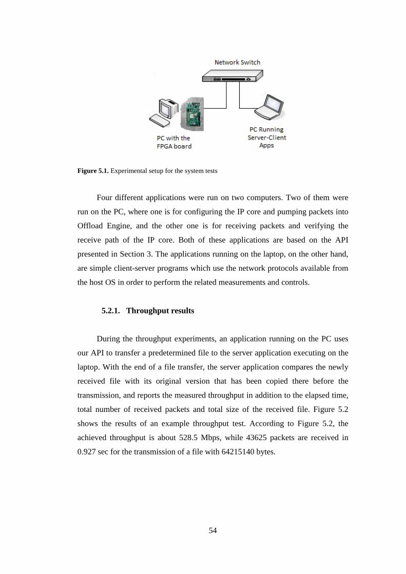
Figure 5.1. Experimental setup for the system tests
Four different applications were run on two computers. Two of them were
run on the PC, where one is for configuring the IP core and pumping packets into
Offload Engine, and the other one is for receiving packets and verifying the
receive path of the IP core. Both of these applications are based on the API
presented in Section 3. The applications running on the laptop, on the other hand,
are simple client-server programs which use the network protocols available from
the host OS in order to perform the related measurements and controls.
5.2.1. Throughput results
During the throughput experiments, an application running on the PC uses
our API to transfer a predetermined file to the server application executing on the
laptop. With the end of a file transfer, the server application compares the newly
received file with its original version that has been copied there before the
transmission, and reports the measured throughput in addition to the elapsed time,
total number of received packets and total size of the received file. Figure 5.2
shows the results of an example throughput test. According to Figure 5.2, the
achieved throughput is about 528.5 Mbps, while 43625 packets are received in
0.927 sec for the transmission of a file with 64215140 bytes.
54

Figure 5.2. Command window output - an example throughput test
After testing the system with different file sizes up to 500 MByte over a
hundred times, the average throughput is obtained as 540 Mbps. Meanwhile, the
maximum achieved throughput is observed as 570 Mbps. In these tests, the MTU
was set to 1472 bytes to achieve the maximum throughput, which results in
splitting files into the MTU-sized packets by Offlad Engine. However, it is a
known fact that the packet size has an impact on the throughput as well.
Consequently, the tests are repeated for different MTU sizes, and the results are
presented in Figure 5.3.
Figure 5.3. The impact of packet size on throughput
0
100
200
300
400
500
600
100 500 1000 1472
Thro
ughp
ut (M
bit/
s)
Packet Size (Byte)
55

The achieved throughput value of 540 Mbps by the IP core proposed can be
attributed to several facts: (i) The file transfer client application on the PC is still
running on the host OS and experiences the overhead related to the OS. (ii)
Xillybus can send data over gigabit speed with its 32-bit interface. But, because of
the uncontinious data provided by Xillybus, the clock domain crossing and data
with conversation by the Xilinx FIFOs, data reaches at a slower speed than the
gigabit speed to Offload Engine.
In order to prove that Offload Engine is capable of providing better data
throughputs than 540 Mbps, a different experimental setup is created. In this
setup, the IP core proposed is slightly modified to be composed of only Offlaoad
Engine and MAC IP core (Xillybus is removed). Then, a hardware application
module on the FPGA instead of an application running on the computer is
implemented to provide data with Offload Engine. In these tests, Offload Engine
achieves a maximum data throughput of 865 Mbps, which is clearly superior.
It should be noted here that actual throughput that can be achieved at gigabit
speed is slightly lower than 1 Gbps. That is, the maximum Ethernet packet size is
1518 bytes (1472 bytes application data, 8 bytes UDP header, 20 bytes IP header,
12 bytes MAC addresses, 2 bytes packet type, 4 bytes CRC). Furthermore, there is
8 bytes preamble and 12 bytes IFG. All of these overheads result in the maximum
achievable data throughput of 957 Mbps. Fortunately, 865 Mbps throughput of
Offload Engine is quite near to 957 Mbps and Offload Engine can be used for
those applications that seek for near-gigabit performance.
Finally, all of these throughput tests clearly prove that the IP core proposed
is working as expected, which further leads to the fact that the send and receive
functions of both UDP and IP protocols are correctly implemented in hardware.
Figure 5.4 shows a wireshark output obtained during a throughput test on the
laptop. According to Figure 5.4, the wireshark observes UDP packets coming
from the source (the PC) with IP address 10.10.96.100.
56
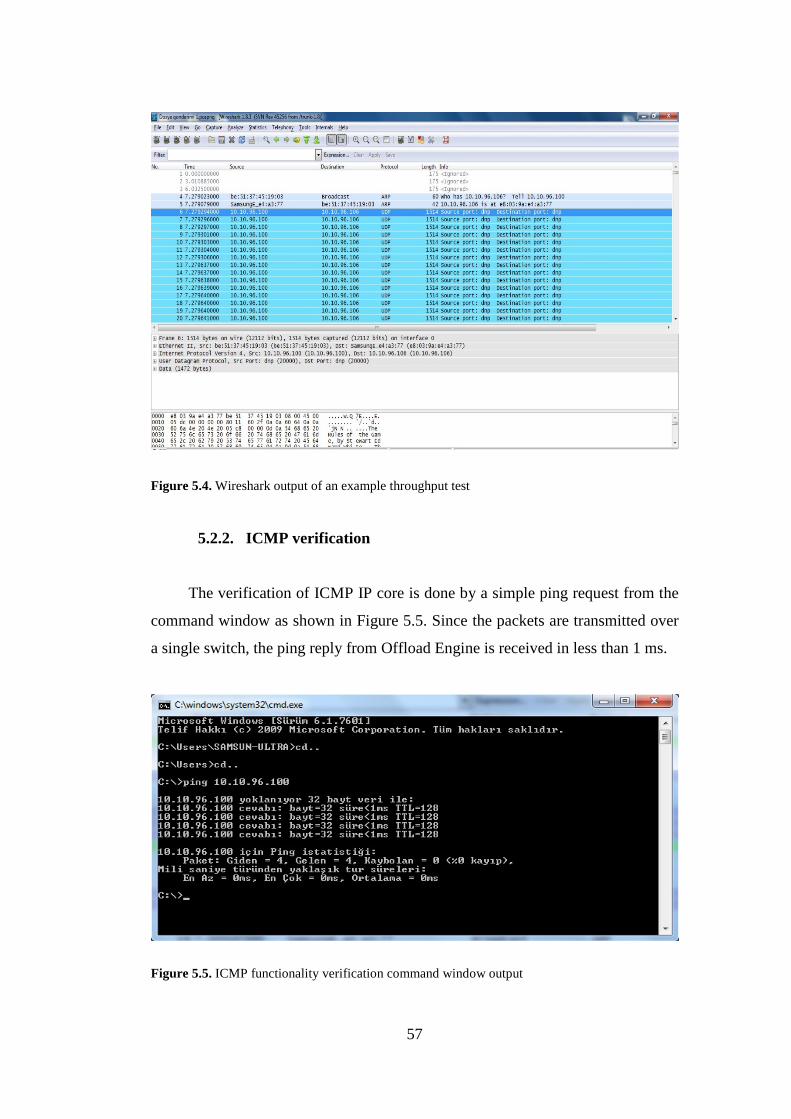
Figure 5.4. Wireshark output of an example throughput test
5.2.2. ICMP verification
The verification of ICMP IP core is done by a simple ping request from the
command window as shown in Figure 5.5. Since the packets are transmitted over
a single switch, the ping reply from Offload Engine is received in less than 1 ms.
Figure 5.5. ICMP functionality verification command window output
57

Figure 5.6. ICMP functionality verification wireshark output
According to Figure 5.6, source 10.10.96.106 (the laptop) sends a ping
request four times, and source 10.10.96.100 (the PC) sends a ping reply
successfully for each request. Based on Figure 5.5 and 5.6, it is concluded that
ICMP IP core is functioning correctly.
5.2.3. DHCP verification
DHCP verification is done by changing the IP address configuration of the
IP core and sending packets with each configuration. In the first case, DHCP is off
and a manual IP address is not given to the PC either. Figure 5.7 shows the packet
transmission under this configuration. It can be seen in Figure 5.7 that source IP
field is 0.0.0.0, which is the default IP address used by the IP core. Since this is
the first data transmission between two computers, there is an ARP request by the
PC before the start of data transmission.
In the second case, DHCP is still off, but a manual IP address
(10.10.96.100) is given to the PC. Figure 5.8 shows the packet transmission with
this configuration of the IP core. It is clear that the received IP packets are coming
from the PC.
58

Figure 5.7. Packet transmission with no IP configuration
Figure 5.8. Packet transmission with manual IP configuration
In the third case, DHCP component is made on, which overrides a given
valid manual IP address (10.10.96.100) in the IP core. Under this scenario, it is
expected that DHCP IP core will lease a new IP address (different from
10.10.96.100) through a DHCP server, and use this address in the subsequent data
communication. Figure 5.8 shows that the packets are coming from a source with
IP address of 10.10.96.90, which is in fact the IP address leased by DHCP IP core
for the PC. Thus, DHCP IP core is proved to working as designed.
5.2.1. ARP verification
ARP packets can be observed in Figure 5.4 for the throughput tests, in
Figure 5.6 for the ICMP tests, and in Figure 5.7 and 5.9 in the DHCP tests. Based
on these figures, it is evident that ARP IP core can broadcast ARP requests to the
network.
Figure 5.9. Packet transmission with DHCP configuration
59

In Figure 5.9, for example, after an ARP request and ARP reply are
observed before the first data transmission by the wireshark, there is no other ARP
request messages present during the transmission of other following packets. This
clearly shows that ARP IP core receives ARP reply messages, creates an entry in
its ARP cache and provides IP Tx with the correct MAC addresses for its inquries.
60
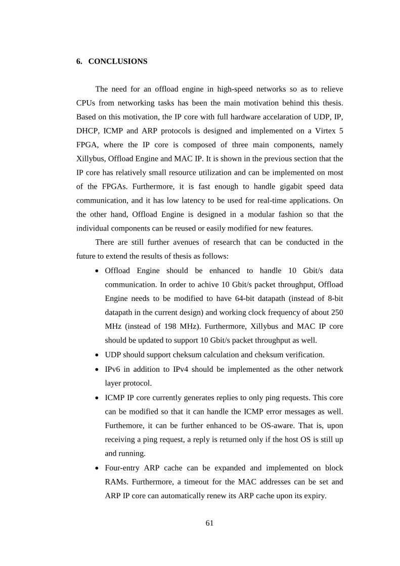
6. CONCLUSIONS
The need for an offload engine in high-speed networks so as to relieve
CPUs from networking tasks has been the main motivation behind this thesis.
Based on this motivation, the IP core with full hardware accelaration of UDP, IP,
DHCP, ICMP and ARP protocols is designed and implemented on a Virtex 5
FPGA, where the IP core is composed of three main components, namely
Xillybus, Offload Engine and MAC IP. It is shown in the previous section that the
IP core has relatively small resource utilization and can be implemented on most
of the FPGAs. Furthermore, it is fast enough to handle gigabit speed data
communication, and it has low latency to be used for real-time applications. On
the other hand, Offload Engine is designed in a modular fashion so that the
individual components can be reused or easily modified for new features.
There are still further avenues of research that can be conducted in the
future to extend the results of thesis as follows:
• Offload Engine should be enhanced to handle 10 Gbit/s data
communication. In order to achive 10 Gbit/s packet throughput, Offload
Engine needs to be modified to have 64-bit datapath (instead of 8-bit
datapath in the current design) and working clock frequency of about 250
MHz (instead of 198 MHz). Furthermore, Xillybus and MAC IP core
should be updated to support 10 Gbit/s packet throughput as well.
• UDP should support cheksum calculation and cheksum verification.
• IPv6 in addition to IPv4 should be implemented as the other network
layer protocol.
• ICMP IP core currently generates replies to only ping requests. This core
can be modified so that it can handle the ICMP error messages as well.
Furthemore, it can be further enhanced to be OS-aware. That is, upon
receiving a ping request, a reply is returned only if the host OS is still up
and running.
• Four-entry ARP cache can be expanded and implemented on block
RAMs. Furthermore, a timeout for the MAC addresses can be set and
ARP IP core can automatically renew its ARP cache upon its expiry.
61

• Different virtual MAC addresses can be assigned to the channels and
DHCP IP core can be changed to lease a unique IP address for each
MAC address so as to create virtual network adapters.
62
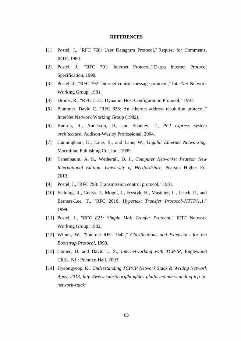
REFERENCES
[1] Postel, J., "RFC 768: User Datagram Protocol," Request for Comments,
IETF, 1980.
[2] Postel, J., "RFC 791: Internet Protocol," Darpa Internet Protocol
Specification, 1990.
[3] Postel, J., "RFC 792: Internet control message protocol," InterNet Network
Working Group, 1981.
[4] Droms, R., "RFC 2131: Dynamic Host Configuration Protocol," 1997.
[5] Plummer, David C. "RFC 826: An ethernet address resolution protocol,"
InterNet Network Working Group (1982).
[6] Budruk, R., Anderson, D., and Shanley, T., PCI express system
architecture. Addison-Wesley Professional, 2004.
[7] Cunningham, D., Lane, B., and Lane, W., Gigabit Ethernet Networking.
Macmillan Publishing Co., Inc., 1999.
[8] Tanenbaum, A. S., Wetherall, D. J., Computer Networks: Pearson New
International Edition: University of Hertfordshire. Pearson Higher Ed,
2013.
[9] Postel, J., "RFC 793: Transmission control protocol," 1981.
[10] Fielding, R., Gettys, J., Mogul, J., Frystyk, H., Masinter, L., Leach, P., and
Berners-Lee, T., "RFC 2616. Hypertext Transfer Protocol–HTTP/1.1,"
1999.
[11] Postel, J., "RFC 821: Simple Mail Tranfer Protocol," IETF Network
Working Group, 1982.
[12] Wimer, W., "Internet RFC 1542," Clarifications and Extensions for the
Bootstrap Protocol, 1993.
[13] Comer, D. and David L. S., Internetworking with TCP/IP, Englewood
Cliffs, NJ.: Prentice-Hall, 2003.
[14] Hyeongyeop, K., Understanding TCP/IP Network Stack & Writing Network
Apps, 2013, http://www.cubrid.org/blog/dev-platform/understanding-tcp-ip-
network-stack/
63
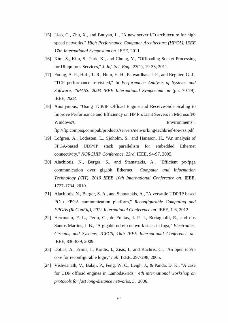
[15] Liao, G., Zhu, X., and Bnuyan, L., "A new server I/O architecture for high
speed networks." High Performance Computer Architecture (HPCA), IEEE
17th International Symposium on. IEEE, 2011.
[16] Kim, S., Kim, S., Park, K., and Chung, Y., "Offloading Socket Processing
for Ubiquitous Services," J. Inf. Sci. Eng., 27(1), 19-33, 2011.
[17] Foong, A. P., Huff, T. R., Hum, H. H., Patwardhan, J. P., and Regnier, G. J.,
"TCP performance re-visited," In Performance Analysis of Systems and
Software, ISPASS. 2003 IEEE International Symposium on (pp. 70-79).
IEEE, 2003.
[18] Anonymous, “Using TCP/IP Offload Engine and Receive-Side Scaling to
Improve Performance and Efficiency on HP ProLiant Servers in Microsoft®
Windows® Environments”,
ftp://ftp.compaq.com/pub/products/servers/networking/techbrief-toe-rss.pdf
[19] Lofgren, A., Lodesten, L., Sjöholm, S., and Hansson, H., "An analysis of
FPGA-based UDP/IP stack parallelism for embedded Ethernet
connectivity," NORCHIP Conference, 23rd. IEEE, 94-97, 2005.
[20] Alachiotis, N., Berger, S., and Stamatakis, A., "Efficient pc-fpga
communication over gigabit Ethernet," Computer and Information
Technology (CIT), 2010 IEEE 10th International Conference on. IEEE,
1727-1734, 2010.
[21] Alachiotis, N., Berger, S. A., and Stamatakis, A., "A versatile UDP/IP based
PC↔ FPGA communication platform," Reconfigurable Computing and
FPGAs (ReConFig), 2012 International Conference on. IEEE, 1-6, 2012.
[22] Herrmann, F. L., Perin, G., de Freitas, J. P. J., Bertagnolli, R., and dos
Santos Martins, J. B., "A gigabit udp/ip network stack in fpga," Electronics,
Circuits, and Systems, ICECS, 16th IEEE International Conference on.
IEEE, 836-839, 2009.
[23] Dollas, A., Ermis, I., Koidis, I., Zisis, I., and Kachris, C., "An open tcp/ip
core for reconfigurable logic," null. IEEE, 297-298, 2005.
[24] Vishwanath, V., Balaji, P., Feng, W. C., Leigh, J., & Panda, D. K., "A case
for UDP offload engines in LambdaGrids," 4th international workshop on
protocols for fast long-distance networks, 5, 2006.
64
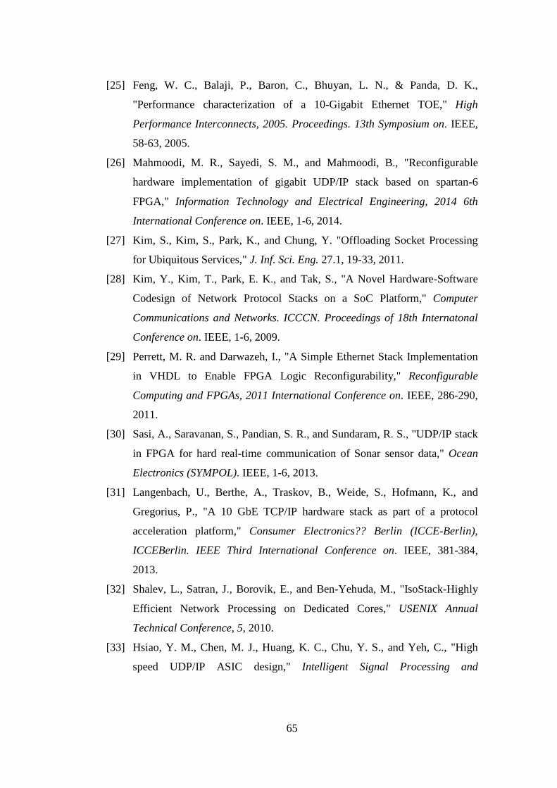
[25] Feng, W. C., Balaji, P., Baron, C., Bhuyan, L. N., & Panda, D. K.,
"Performance characterization of a 10-Gigabit Ethernet TOE," High
Performance Interconnects, 2005. Proceedings. 13th Symposium on. IEEE,
58-63, 2005.
[26] Mahmoodi, M. R., Sayedi, S. M., and Mahmoodi, B., "Reconfigurable
hardware implementation of gigabit UDP/IP stack based on spartan-6
FPGA," Information Technology and Electrical Engineering, 2014 6th
International Conference on. IEEE, 1-6, 2014.
[27] Kim, S., Kim, S., Park, K., and Chung, Y. "Offloading Socket Processing
for Ubiquitous Services," J. Inf. Sci. Eng. 27.1, 19-33, 2011.
[28] Kim, Y., Kim, T., Park, E. K., and Tak, S., "A Novel Hardware-Software
Codesign of Network Protocol Stacks on a SoC Platform," Computer
Communications and Networks. ICCCN. Proceedings of 18th Internatonal
Conference on. IEEE, 1-6, 2009.
[29] Perrett, M. R. and Darwazeh, I., "A Simple Ethernet Stack Implementation
in VHDL to Enable FPGA Logic Reconfigurability," Reconfigurable
Computing and FPGAs, 2011 International Conference on. IEEE, 286-290,
2011.
[30] Sasi, A., Saravanan, S., Pandian, S. R., and Sundaram, R. S., "UDP/IP stack
in FPGA for hard real-time communication of Sonar sensor data," Ocean
Electronics (SYMPOL). IEEE, 1-6, 2013.
[31] Langenbach, U., Berthe, A., Traskov, B., Weide, S., Hofmann, K., and
Gregorius, P., "A 10 GbE TCP/IP hardware stack as part of a protocol
acceleration platform," Consumer Electronics?? Berlin (ICCE-Berlin),
ICCEBerlin. IEEE Third International Conference on. IEEE, 381-384,
2013.
[32] Shalev, L., Satran, J., Borovik, E., and Ben-Yehuda, M., "IsoStack-Highly
Efficient Network Processing on Dedicated Cores," USENIX Annual
Technical Conference, 5, 2010.
[33] Hsiao, Y. M., Chen, M. J., Huang, K. C., Chu, Y. S., and Yeh, C., "High
speed UDP/IP ASIC design," Intelligent Signal Processing and
65

Communication Systems, 2009. ISPACS 2009. International Symposium on.
IEEE, 405-408, 2009.
[34] LogiCORE, I. P. "Endpoint Block Plus v1. 14 for PCI Express," 2011.
[35] Xilinx, "ML505/ML506 Evaluation Platform." UG347 (v2. 4) edn 176,
2007.
[36] Anonymous, "Xillybus Product Brief,"
http://xillybus.com/downloads/xillybus_product_brief.pdf, 2014.
[37] Xillybus, IP core factory, 2010. http://xillybus.com/ipfactory/
[38] Xilinx, "Virtex-5 FGPA Embedded Tri-Mode Ethernet MAC User Guide,"
2011, www.xilinx.com/support/documentation/user_guides/ug194.pdf
[39] Schaumont, P. A practical introduction to hardware/software codesign.
Springer Science & Business Media, 2012.
[40] Xilinx, I. S. E., "14.2 Software Manuals: Constraints Guide, and
Development System Reference Guide, Xilinx," 2012.
66