design and implementation of a real time fpga based vga ...peterbrewster.co.uk/dissertation.pdf ·...
TRANSCRIPT

University of Bolton
AMI5001
Design and implementation of a Real Time FPGA
based VGA Spectrogram display system.
Dissertation
Student Peter Brewster
Academic Supervisor Kevan Smart
Revision Published 10 May 2013
Abstract: Dissertation documenting research around commercial and technical aspects of a Real Time, FPGA based Spectrogram
generation and display system. Gives special attention to application in cardiology. Details design and development of components to
build such a system.

Acknowledgements:
Kev Smart for support throughout project.
University of Bolton for development hardware.
Altera for the excellent 'Quartus' design suite.
Dr Lee for copy of Introductory text on ECG.
Dr Kendall for his time discussing practicalities of ECG in General Practice.
Adrian Grindon for supply of TI evaluation board.
The Document Foundation for 'Libre Office' suite – especially the formula editor!
Creators of 'subversion' repositry server, and 'tortoise' the subversion client.
Jim Peters, author of View filter creation software
…..And of course Louise and Owen for not suggesting I throw the towel in when it
would have been so easy to do so.

Contents
1 Introduction
2 Definition of Terms in Project Title
2.1 Real Time
2.2 FPGA
2.3 VGA
2.4 Spectrogram
2.5 Display System
3 Project Status/Executive Summary
4 History and general background to ECG
4.1 Brief History of ECG
4.2 Description of ECG trace
4.3 Application of spectrogram in ECG analysis
5 Other Background Study
5.1 Literature Review
5.2 Some examples of other applications of spectrogram
5.2.1 Speech Therapy.
5.2.2 Machinists 'chatter detector'.
5.2.3 Seismology.
6 Feasibility
6.1 Interview summary with Dr Kendall
6.2 Overview of other existing tools for generating spectrogram
6.3 Feasibility summary conclusion

7 High level design of system
7.1 Power Supply
7.2 System I/O
7.3 User Interface
7.4 Outline Architecture Design
7.5 Agency Requirements
7.6 Detailed Architecture Design
8 Derivation of Hardware requirements
8.1 ADC – Bandwidth of analogue to digital converter
8.2 Display (memory) requirements
9 Design Tool Selection
9.1 Hardware platform selection
9.2 Software design tool selection
10 Evaluation of mathematical method of generating spectrogram
10.1 Fourier transforms
10.2 Banks of filters
10.3 Fourier Transform
10.3.1 Wavelet Transform
10.4 Comparison of Filter Bank and FFT methods of computing spectrogram
10.4.1 Filter Bank spectrogram computation
10.4.2 FFT Spectrogram computation
10.5 Conclusion
11 Display Design overview
11.1 Display Layout
11.2 Spectrogram display format

12 Design activity log – Display
12.1 Display System Block Diagram
12.2 Low level VGA driver
12.2.1 Horizontal Synch pulse
12.2.2 Vertical Synch pulse
12.2.3 Integration and verification of Synch Pulse generators
12.3 Generic Display Element
12.4 Integration of display elements and low level driver
12.5 Integration tests and demonstration
13.1 Spectrogram computation high level design
13.1.1 Block Diagram
13.2 Description of items in block diagram
13.2.1 FIFO (circular buffer)
13.2.2 Window Function
13.2.3 FFT
13.2.4 Post Process
13.3 Management of data from the maths block to display interfaces
13.4 Design of sub entities in 'Math Block'
13.4.1 Note on change of resolution.
13.4.2 Design and test of FFT controller.
13.4.3 Design and test of Pre-processor.
13.4.3.1 Design of window function
13.4.3.2 Design of Buffer and 'Slicer
13.4.4 Design of post processor
14 Integration and test
15 Conclusions and Suggested further work.
Bibliography
Appendix A Source Code For Sinc filter development programme.
Appendix B VHDL Listings and Quartus project download instructions.
Appendix C Miscellaneous tools.

1 Introduction.
This dissertation documents the research, experimentation, specification and
design of a system intended to produce a spectrogram of some signal, using a standard
VGA monitor as the output device.
The project, especially in the early stages, makes reference to its use in ECG
('heart monitoring'). While this was the initial context for the project, it is by no means the
only application. Other applications may include machinists, engine manufacturers,
speech therapists, musical instrument manufacturers, amongst others.
While these are given some consideration, the field of ECG is given greatest attention, this
field is used to derive system requirements, such as sample rate, memory requirements,
etc.
The research aspect of the project includes a review of xisting tools to generate a
spectrogram. There will also be some review of viability of this (the system designed in
the project) as a commercial product, agency requirements, etc. Since the project is
fundamentally an academic\technical one, design will continue even if the findings suggest
that the design is not commercially viable.
The design phase of the project largely runs concurrently with the research and
experimental aspects. Design is also likely to continue beyond the completion of the
substantial part of this dissertation, as enhancements and optimizations of the system are
implemented

2 Definition of terminology
A number of the terms used in the dissertation title are clarified here. These are given
here in the order they are presented in the title
2.1 Real Time
In this context, Real Time refers to the fact that the system is processing an input that
has no defined end time, and is providing an out put at a rate that matches the input.
Ideally 'Real Time' implies that there is no delay between input and output, but clearly this
is not possible. What is taken as the qualification for real time is that any lag or delay in the
system is of no consequence. In this case, of an instrument used by a human operator, if
any delay is barely perceptible to the user, it may be considered to be real time.
The context is key to this definition, for example fighter jets may contain real time
systems, but the suggested limit of 'barely perceptible to user' would seem to be
inadequate, with it's requirement to modify behaviour rapidly in response to external
factors.
2.2 FPGA – Field Programmable Gate Array .
This is the technology that will be used to develop the system. It refers to an
integrated circuit with a multitude of gates and registers that may be configured to perform
functions defined by the designer. FPGA's are volatile (blank at power on) and typically
'boot' from a small non volatile memory device that contains the details of the gate and
register assignments. FPGA's are used as development platforms (prior to migration to
ASIC) and as components in the final products. FPGA's are not to be confused with
microcontrollers. While they are usually programmed using what appears to be a fairly
high level language, this language is hardware definitions, not software instructions.
Microprocessors may be implemented on FPGA with an appropriate hardware definition,
and software written for it. In principle, this would be an acceptable route for this project to
meet the title definition, however, this is not how it will be implemented here. To do so
would steer the project towards it being heavily software based, and a computing project
rather than an electronics one.

2.3 VGA
This refers to the ubiquitous monitor used by computers. This is a mature standard,
common across fairly old CRT monitors, right through to modern LCD monitors. A benefit
of using this as the display is that the device itself will not need a dedicated, built in
display. It was stated that VGA is a mature standard, and indeed some modern computers
are moving towards a digital (DVI or HDMI ) display interface. However, the presence of
VGA does seem to remain on many of the machines, and it is anticipated that it will
remain so for some time, even if as a 'legacy' feature.
2.4 Spectrogram
This is a display containing information about the frequency content ('spectral
content') of some given signal. In practice, a spectrogram is a succession of spectra of the
input signal , presented in such way as to allow indication of the change of frequency
content over time. This is distinct from a spectrum, which gives the frequency content of a
snapshot of the input. Spectrogram may be generated and and presented in a number of
ways, which is covered in greater detail in subsequent sections.
2.5 Display System.
It may seem a little pedantic to define ' Display System' here, however there is some
impact on requirements. To describe something as a display system can be seen to
indicate that it does not imply any analysis features. So while a full blown instrument may
have some such features (cursors, graticules, screen dump, etc) it is not required to
implement these here. That does not exclude the possibility that some attempt may be
made to do so.

3 Project Status/Executive Summary
For a number of technical and time related issues, it was not feasible to create a complete
'end to end' spectrogram generation and display system. However, all the substantial
elements for such a system have been designed, simulated, and tested. Integration of
these parts was carried out as far as possible. Demonstration of the system was achieved,
albeit with internally generated data for the input, and severely curtailed resolution on the
output.
Sections 14 and 15 discuss how these limitations may be remedied, and give some
indication of what work would be required to complete the system as a workable product.
It is claimed then that this work contains a functional design that may be used as a
development platform to progress into a fully operation system.
Commercial viability of the system was evaluated .While no immediate, compelling value
was seen, it is clearly indicated in sections 5 and 6 that there are markets to explore. The
system is shown to be a cost effective approach to generating and displaying
spectrograms.

4 History and general background to ECG
It was indicated in the introduction that a target application for the project would be
the study of heart monitoring traces. This section provides a general introduction to that
field. It is given as background reading only, and does not of itself constitute a part of the
project.
4.1 Brief History of ECG
ECG Stands for Electrocardiogram, (or Electrocardiograph). It is a representation of
the activity of the heart derived from the measurement of electrical potentials on the
patients skin. In the late 18th century, Galvani noted ‘Animal electricity’ where the leg of a
(recently) dead frog was made to move under the influence of electricity. While this may
have inspired Mary Shelley (‘Frankenstein’) there was no practical use for that knowledge
at that time (anyone who has been resuscitated by defibrillator would assert that this is no
longer the case). The converse, that movement of muscle creates electrical potentials,
was not noted until around 100 years later. In the early 1920’s, Willelm Einthoven used a
sensitive galvanometer to distinguish electrical potentials on the skin, and was able to
correlate these to the activity of the heart. His work earned him a Nobel Prize. The
terminology that Einthoven created to define the states of the heart beat are still in use
today.
4.2 Description of ECG trace
The ECG trace is a recording of electrical activity on the surface of a patients skin. It
cannot be assumed that the heart is the sole contributor to the potentials measured,
however, steps are taken to make this the case as far as possible, including the positioning
of the electrodes at specific places, and exhorting the patient to remain as still as possible.
External sources of noise (e.g. mains 50Hz) are taken into consideration. ECG machines
traditionally used a moving pen to record the trace(s) on a rolling sheet of paper. This has
been superseded by electronic display equipment, very similar in nature to an
oscilloscope. Each beat of the heart is not a simple, single pulse, there are several stages
involved, ventricular and atrial contractions and relaxations, each giving rise to some
named features. An idealised ‘text book’ trace would resemble fig.1, below.

Fig 4.2A Idealised ECG trace
This is repeated with a period typically in the order of 1Hz (the heart rate being
monitored).
To analyse the ECG, a system of naming the parts was devised by Einthoven. A stylised
drawing, fig. illustrates the major parts of this system.
Whilst there is no real need to go into clinical detail, these points are referred to in
an anatomical context for possible future reference. The peak at P is indicative of the
contraction of the atria of the heart. This is a relatively small muscle mass, so a small peak
would be expected here. The QRS section is treated as a single entity, and is referred to
as the ‘QRS’ complex. This represents the contraction of the ventricles, the larger muscle
mass of the heart. The ‘T’ wave is caused by the ventricles relaxing. This relaxation phase
is often referred to as ‘repolarisation’. The QRS complex has some specific details around
it’s naming. These names are quite specific to conventional ECG analysis, however they
may form a useful reference later. If the first deflection is downwards, it is called a Q wave.
T
Fig 2 Idealised ECG trace, with Eintoven’s annotation
Fig 4.2b

Any deflection upwards is referred to as an R wave, whether or not it is preceded by a Q
wave. Any deflection below the base line, following an R wave, is referred to as an S wave,
again, regardless of whether or not there was a preceding Q wave.
It should be noted that, in the larger context of this project, the references to the direction
of displacement may well be irrelevant, as this information is lost by a spectral analysis. It
should also be noted here that the above is a simplified and idealised view of the ECG. In
practice, up to twelve electrodes, on different areas of the chest and limbs, may be
simultaneously monitored and cross compared.
4.3 Application of spectrogram in ECG analysis
Cardiac conditions may be diagnosed by considering the relative amplitudes,
duration, and qualitative shape of the ECG. The time between features may also be an
indicator of some conditions. Additionally, any features (peaks, troughs) that do not fit into
the model may be judged to indicate the need for further examination.
Transforming the data to the frequency domain allows features that may remain
hidden under the noise floor to present themselves as frequency content. A spectrum may
indicate a peak for that frequency. A spectrogram, being a series of spectra taken of the
signal, each spectra over a fixed time window, permits features to be associated with a
position in the P-QRS-T ,in a manner that a simple spectral analysis may not. It also
permits the repetition of a spectral peak to be noted clearly.
A note of caution – due to the nature of the transformation, there is a trade off
between the precision of the time (positional) and frequency information. This is because
each spectrum is composed of samples taken from a discrete and fixed duration. A narrow
sampling window permits the position of a feature to be known accurately, (it must exist
within that window) but it’s frequency content to be less precise (one may take a simplistic
view that this is simply due to their being less samples, but it is deeper than that:- the
longer the period over which samples are taken, the greater the range of frequencies that
may be observed). Some comparisons have been made to Heisenberg uncertainty (in that
frequency content or time of event may be known accurately), however this is perhaps
fanciful, it is not that the act of observation is affecting the data, as opposed to the manner
of observation.

5 Other Background Study
5.1 Literature Search
An attempt was made to gauge academic interest in the area of applying
spectrograms in ECG analysis and cardiology in general, and use of FPGA in spectrogram
creation.
An abundance of papers covering the mathematics of performing FFTs in FPGA's was
found. While these where useful reading, they were not in themselves a great contribution,
as it was decided during the project to utilise an available FFT engine. No papers were
found documenting projects very similar to this one, in particular performing the transform
and displaying it. This is by no means a claim that non exist, just none found by the author.
A further search found 423 articles and papers with containing the key words 'spectrogram'
and 'cardiology', and 117 articles containing 'FPGA' and spectrogram were found.
Abstracts were read. A selection of some findings are discussed below, where a particular
relevance was found.
5.1.1 FPGA realization of a CORDIC based FFT processor for biomedical signal
processing
Ayan Banerjee,Anindya Sundar Dhar, Swapna Banerjee Department of Elecronics and
Electrical Communication Engineering, Indian Institute of technology, Kharagpur, Feb
2001
This article discusses a means of efficiently generating FFT of data, in the context
of biomedical technology. The method described is not directly relevant to the means of
implementing this project, and does not actually dispay spectrograms. It does contain
some passing, contextual references to ECG as well actual physiological conditions. This
may be a valuable article if one were starting from first principles on the transform itself.
5.1.2 Heart energy signature spectrogram for cardiovascular diagnosis
Vladimir Kudriavtsev, Vladimir Polyschuk, and Douglas L Roy , BioMedical Engineering
OnLine. 2007, Vol. 6, p16-37
At first glance, this article appears to be not relevant, as it is looking at
cardiophonograms, (audio recordings of the heart) as opposed to electrocardiograms.
However, since it is looking at broadly similar frequency domain and concerned specific

heart defects, it was studied. This paper presents a methodology that may be followed in
characterizing defects by the spectrograms. It was also of interest in that it caused the
author to consider the possibility of attempting to correlate cardiophonograms and ECGs.
The project here would be capable of creating spectrograms of both types of data, with
minimal hardware modifications. Hence this is indicated a further potential application.
5.1.3 Enhancement of time-frequency properties of ECG for detecting
micropotentials by wavelet transform based method
By Hüseyin Tirtom; Mehmet Engin; Erkan Zeki Engin. In Expert Systems With
Applications. 34(1):746-753
This paper provides a good coverage of the motivation to transform ECG into
spectrogram format – issues of low amplitude signals are discussed. The paper then
discusses an end to end system. Reference is made to some interpretation features, in
that it suggests employing a 'QRS detection block', although it does not give great detail
on how to achieve this. The paper then continues with a demonstration of how some small
signals (Late potentials) are identified.
5.2 Other applications of spectrograms
This section exists as an aside to the main body of the project . Its purpose is to
identify other fields in which spectrograms, of similar bandwidths to the ECG, are, or maybe,
used. This is regardless of how they are generated, and whether or not they are required in
real time. The purpose of the exercise is to identify other potential markets for this
technology. The list does not represent an attempt at exhaustive research, it is some
examples readily found. Some elements of this section are speculative.
5.2.1 Speech Therapy
Speech therapists do already use real time spectrograms in a therapeutic setting.
The National Centre for Voice and Speech (Utah University, USA) defines two categories of
spectrogram as useful, 'Wide Band' which it defines as having a bandwidth of 300-500Hz,
and 'Narrow Band' which it defines as bandwidth of 45-50Hz. Note that these definitions of
wide and narrow band are in the context of that field. These band widths are certainly within
a the area of the ecg, perhaps a little higher, but certainly caputurable with a 1Khz sample
rate. The use of Spectrograms in speech is to provide a fast, real time, 'bio feedback' path,
for the patient to modify their speech pattern in response to visual cues, as opposed to

auditory ones. This may be for a defect or to improve articulation.
5.2.2 Machinists 'chatter detector'
Machinists, ie persons operating rotary mechanical cutting machines (where either
the work or the tool is is rotated) may wish to optimize cutting speed by setting the speed as
close to, or above, the point at which chatter occurs. Chatter is vibration in the tool and work,
and is a function of the speed, tool configuration ('number of teeth') and feed (advance rate).
The vibration can be damaging to the tool and the work, potentially catastrophic. Machinists
have traditionally done this to some extent 'by ear', an art rather than a procedure. This
would require them to dispense with ear defenders, a potential cause of harm. A 'chatter
detector' would permit an optimum cutting rate to be set without having to go through a
chatter region. In 2001, an algorithm devised by Prof Ridgeway of Sheffield University was
implemented in a DSP device. The author had the privilege of contributing (as a
subcontractor, GSPK Design, Knaresborough) some part of the user interface to a prototype
of this device. At the time, it was intended to be a hand held device with a minimal user
interface. This did not directly output any spectral information, it was processed internally,
and directed the user to settings. It is suggested that there may be an application for live,
real time spectrograms in the optimization of tooling speeds, in a dynamic manner, the
operator being able to experiment 'live' with the machine settings.
5.2.3 Seismology
The United States Geological Survey (USGS) provides a constant feed of
spectrograms derived from data from seismology sites around the US. It describes the
relevant vibrations as being in the region of 0 – 10 Hz, which is very comfortably within the
domain of this FPGA system. The USGS uses these to monitor and locate earthquakes in
the US and around the world. There is ongoing research as to how to apply then information.
This is very much a real time application, as it is now possible to warn ahead (electronically)
that a shock wave is approaching. This may only provide minutes or seconds notice, but
may be sufficient to (e.g.) shut down a gas supply or reduce risks where possible. Arguably,
by reducing the cost and power supply requirements of the monitoring equipment, the
quantity and quality of data could be improved.

6 Feasibility
6.1 Interview summary with Dr Kendall (GP)
An opportunity arose to interview a practicing GP . This was intended as a
qualitative exercise. As well as being a GP, Dr Kendall is engaged with modern technology,
for example he demonstrated an I-phone app that can take a pulse. Additionally, while not a
cardiology specialist, he was one of the proof readers of Hampton's work 'Introduction to
ECG.' The interview was not especially structured, and was conducted by a series of e-mails
and conversations.
Ahead of the interview, Dr Kendall was given a very short introductory text on what
spectrograms are. It is not known if this was read, but the answers do indicate sufficient
appreciation to disregard this as a concern. The following text, in italics, is a compilation of
answers to direct questions, plus some free-range comments of his own. Typographical
errors have been corrected, but otherwise nothing has been changed. Dr Kendall often used
the phrase 'in GP land '. This was clarified to mean 'in a typical General Practitioners
surgery'.
….
I'll give you a snapshot of how we (GP’s) use ECG’s and their existing limitations as well as
the trends ... secondary care (Hospitals) hopefully as objectively as possible ..- other
GPs/Drs will have other views)....
….Modern day ECG machines are vastly superior to the old lumbering machines of 20years
ago when I was training.
They are all small (or at least, small ones are available) and portable and can be powered
by battery and mains. I'm sure you can probably get them to plug in to an iphone now - they
certainly can seamlessly integrate in to clinical computer systems in GP land.
Most modern ECG machines (circa 2005+ ... have some degree of interpretation function
built in...they print it (or export it to a PC) and then interpret it. IE. they make a judgment
whether it is normal, abnormal and then define the abnormalities - usually fairly well - ….
Most GP surgeries will have an ECG machine already and be quite comfortable with its use
and limitations. ..
GP’s primarily use ECG’s to diagnose rhythm problems ..in patients - essentially we use
them to determine if the p waves are regular/irregular. Having a higher definition on the
structure of the p wave would add nothing to this basic use of an ECG ….. The basic
waveforms produced by the ECG are more than adequate to diagnose a raft of rhythm and
conduction type problems .. ("Left Ventricular Hypertrophy" for instance)....

Most Chest Pain ( is this a heart attack?) patients would be sent to hospital …. so that
diagnostic use is falling out of favour.
We actually use the local hospital service exclusively for ECG’s now - they provide a same
day service to us with interpretation.
There has been a real shift in secondary care practice in the last 10+ years. ECG’s seem to
play far less of a role in diagnosis now than they used to do - and seem to be used as a
screening tool - other technologies are then employed to diagnose problems (Stress tests,
Myoview scans, MRI Angiograms, Echocardiograms for instance). The need to use an ECG
to get really clever and diagnose minutiae has passed, ..
..My first thought with this is 'What problem do I currently have with ECGs/cardiology that
having a new / higher definition way of interpreting an ECG will fix?".
My answer would be, there isn't one... and let the hospitals get clever with new
technology......do I feel like a newer ECG approach is worth my time and money to buy in
to ? No...
….. I just don't think it is an improvement that is needed at the moment (in GP land) as the
kit we have is fine? I guess it's too 'evolutionary' as a cardiological technique and not
'revolutionary' enough?
The largest market for ECG machines would be GP’s (I'd have thought) - purely by the sheer
number of primary care facilities versus specialist hospital clinics/wards.
…...
Dr Kendall then closed with some supportive comments and a discussion on research ethics
where patients are involved.
The indications from Dr Kendall were that in the largest (by volume) market for ECG's there
appears to be no real demand for such a system. The suggestion ” too 'evolutionary' as a
cardiological technique and not 'revolutionary' enough? ” perhaps sums it up well. There is a
certain inertia, particularly at GP level, that would need to be overcome. Without having a
known problem to solve, it is difficult to achieve this. It is restated, however, that this section
is presented as qualitative, background information, and is based on the opinion of a single
practitioner.

6.2 Overview of other existing tools for generating spectrograms
There are a whole host of means of generating and displaying spectrograms.
Modern spectrum analysers and the higher end of digital oscilloscopes now may provide
this feature. Software, commercial and open source, exists on numerous platforms, (PC,
Android, Apple) that claims to be capable of providing real time spectrograms.
Some cases are viewed here. This is by no means an exhaustive search, however it is
believed that it catches the corner cases of appropriate technology at the time of writing.
6.2.1 Textronix RSA-5000 series Spectrum Analyser
Available since January 2013, this is defined as a mid range spectrum analyser.
This is primarily targeted at RF engineers. Offers 110MHz bandwidth, in 26.5 and 15GHz
model. This offers a real time spectrogram feature. The specifications clearly outstrip the
requirements for ECG (Section 8). The price tag may also be problematic, at £32,000.
An example has not been seen, but the author has some familiarity with this type of
equipment, they are by no means portable or discrete. This item was not included as
viable alternative to the proposed system, but provided as an indicator of the higher end of
equipment.
6.2.2 GW-Instek GSP-930
GW Instek is a brand of GoodWill Instrument Co, a Taiwanese firm that have been
in existence since 1975, although are relatively emerging (in the west) at the higher end of
instrumentation .This is a 3GHz model, somewhat more compact than the Tektronix part,
above. At 4.5 Kg it is perhaps not quite portable. Again, this far outstrips the requirement.
At a price of around £3660, it is somewhat more viable on a cost basis.
6.2.3 Texas Instruments ADS1x98 ECG FE
This is an evaluation board that Texas Instruments make available to evaluate their
ADS1x98 series of ECG front end amplifiers . This is coupled with a general purpose DSP
board for demonstration purposes. Adrian Grindon, a field application engineer for Texas
Instruments, kindly made such a unit available. It ships with software that is capable of
generating spectrograms, which are claimed to be real time, however they are delivered by

USB to a host computer, introducing some lag. Despite that, it would appear that the
additional resources to output from the DSP to a VGA monitor would not be too onerous, a
very low end graphics chip set should be able to do this. No firm pricing was available, as
this was a commercial /engineering sample. Mr Grindon suggested that the evaluation
board as is would be “a few hundred dollars” (although given freely to customers). No
actual BOM cost was available, so this budgetary figure is accepted for discussion.
6.2.4 Spectrum View Plus' I-os (Apple) platforms.
No device was available to evaluate this product. Its is targeted at audio range signals,
which would place it very well in the frequency range of interest. The product web page
shows screen shots which appear quite satisfactory. A customer review seems to suggest
it functions well, however only one review was visible (at the time of writing). The software
costs £4.99 . This of course requires the user to own an IOS device. The input is defined
as microphone, so some adaptation would be required to the patients electrodes.
Portability is clearly not an issue, neither is price (assuming prior ownership of hardware).
(Spectrum Plus View may be found at www.oxfordwaveresearch.com or search on the
Apple 'App store' )
6.2.5 Wavesurfer (Personal computer, Windows or Macintosh)
This is a free, open source program that is popular with speech therapists. Again, being
audio range, is appropriate in terms of frequency domain. It claims to give real time
spectrograms. As it is computer based, it should be feasible to use a 'line in' rather than a
microphone, however, some circuitry would still be required, although not as sophisticated
as the needed in all the other instances. Use of a laptop would make it portable, and
perhaps in practical usage, more closely resemble the system described by this project.
( wave surfer may be downloaded from http://www.spectrogramsforspeech.com/tutorials-
2/software-download-2/)

6.2.6 Conclusion
All of the above, with the exception of the Texas Instruments evaluation board,
would require some additional electronics to interface to the patient electrodes. However
since this is also the case for the FPGA based system, this tends to be a zero sum
element of the comparison. What has been omitted is the fact that a real world system
may be required to monitor and transform multiple channels simultaneously. In the case of
the spectrum analysers put forward, this would require one machine per channel, clearly
impractical. In the case of the software, this would be limited by available processing
power of the platform. The relatively low processing power of the Apple devices is unlikely
to meet this, however, a powerful personal computer, perhaps supported by additional
GPU's as co-processors, would have little difficulty in meeting this. This does then of
course devolve the problem back to specialist hardware and software.
The Texas Instruments offering does seem to be a viable option, although the work
required to make it truly 'stand alone' is unknown.
The FPGA solution, as proposed by this project, is assessed. Altera are currently
offering (at low volume pricing) the EPC20F484C8 for $47 ( £30.35 ) The cost of external
memory is small compared to this, (Taiwanese spot price at time of writing is $1.53 for
2GB DDR 3, or approximately £1.)
A reasonable estimate of the build cost of the FPGA based system would be
comfortably below £100. It would be safe to budget for an increase in cost of £50 to add
per additional channel, so it is claimed that an 8 channel system could easily be built for
£450.
This certainly compares favourably with a high end, specialised PC, but perhaps not
so well with a generic 'beige box' PC.
It might be observed that Moore's “law” will eventually cause the PC to be more
cost effective. However, this is moot, as the process used in fabricating FPGA's follow
similar trends.
6.3 Feasibility conclusion and suggested market strategy
There seems to be a conflicted view as to the market demand for the system as a
product, some academic interest shown in section 4.3, and the other applications indicated
in Section 5, against the pragmatic view point of a practitioner (section 6.1)
A classic market behavior for new products is of the 'early adopters' paying a higher
price, followed by acceptance in the mass market, as price is seen to reduce, and the 'early
adopters' evangelize the product. In this case, the early adopters may be the Cardiology
consultants and specialists, perhaps in private practice or NHS. The mass market would be
of course the GP's . The GP's may purchase the items as discretionary purchases, or as
replacements for old equipment.
The is another potential marketing strand which may help increase volume of
production. Section 5 discussed other applications of spectrograms. These are, in the main,
single channel applications. This may permit a single device to be pitched to multiple
markets. Since this would be the single channel device, retailing for (around) £250 could well
be in the range for operators to consider these as discretionary purchases, and indeed worth
purchasing to evaluate. So in addition to creating new markets, this may generate sufficient
sales and revenue to achieve the sort of purchasing volume that may bring pricing of the
multiple channel device down.
A further benefit of accessing other application markets would be to provide wider
acceptance of this type of technology, in a less critical sector, potentially ' normalizing' the
use of spectrograms, which may help overcome inertia in medical sectors as there would be
other case studies to point to.
It is concluded, but with caution, that the FPGA spectrogram system does seem to
have viable market places, even if not necessarily in the field initially suggested. It is noted
that there would be significant further and detailed market research to be conducted. There
is also a considerable amount of engineering work remaining to make this a realisable
product.

7 High level design of system
7.1 Power Supply:
The voltage and current requirements of the system remain unspecified at this
stage, and will be derived from hardware design decisions. However, as the finished
product is intended to be in physical contact with people, it will be assumed that the
system will operate from a low voltage, mains isolated supply, or batteries. A nominal
supply of 5V at 1A is given here. This does not include the supply for the VGA monitor,
which is assumed to have it’s own mains supply. Further issues around power supply are
addressed in section 7.5, Agency Requirements.
7.2 System I/O
This is defined by the nature of the system itself, however some values are placed here
Inputs (ECG trace) – Analogue input, 1V peak to peak, band width limited to 22KHz
(typical audio system ‘line’ levels.
Outputs – VGA data, 640 x 480 pixels.
7.3 User Interface
There is no need for a sophisticated user interface – the simplest implementation
would be for the system to create a spectrogram on reset, and continue scrolling the
display.
Id Type FunctionReset Push Button Reset whole system, take initial spectrogramHold Push Button Freeze the display Screen Dump* Push Button Capture the display and send a file via RS232 for
permanent copy offline
*Screen Dump is a complex feature, that is proposed here as something that may be
desirable in a real product, but is unlikely to be implemented in this project.

FPGA
ADC PreProcessor
Spectrogram Generator
VGA DAC
VGA Memory
VGA Controller
V
GA
Con
nect
or
7.4 Outline Architecture Design
Diagram here is a very high level diagram showing the substantial blocks that the system
is expected to consist of. This is a steering concept, any final design is not forced to
comply to this initial plan.
Fig 7.4 Proposed system structure
7. 5 Agency Requirements
Electronic (and other) products sold within the EU member states must comply to
some applicable standards, covering safety (Low Voltage Directive) and electromagnetic
compatibility (EMC directive). Identifying, and demonstrating compliance to, the
appropriate safety and EMC standards permits the product to be marked with the CE logo.
Some products (IT equipment, lighting, power tools, etc) are in categories with clearly
defined standards to meet. Medical devices have been identified as one such category.
A specific EEC Council Directive (93/42/EEC) Article 1, section 2(a) states.
“ ‘medical device’ means any instrument, apparatus, appliance, material, whether used
alone, or in combination, including the software necessary for it’s proper application
intended by the manufacturer to be used for human beings for the purpose of:
- diagnosis, prevention, monitoring, treatment or alleviation of disease,
……”
ECG signal

the standard then goes on to name other purposes. It would seem clear that the system
being designed here, if placed on the open market in the EU (or indeed world-wide, as
obtaining CE compliance does permit, or certainly ameliorate, entry to many non-EU
markets) would fall under the scope of this directive.
The full directive is a long and complex document. The essence is that medical devices
require CE marking, and hence must comply to some set standards. Given that the
technological scope of medical devices is wide – from the high energy, high voltage
defibrillator, to an inspection mirror, it is meaningless to repeat the whole documents here.
Some sections do warrant close attention, as they have specific relevance. The following
extracts are taken from Sections 10 and 12 of Annexe 1 ‘General Requirements’ of the
directive (93/42/EEC). The section number and title are quoted, the accompanying text is a
summary of that section.
10 Devices with a measuring function.
Where it is stated that devices with a measuring function are sufficiently accurate and
stable for the purpose, the limits of the accuracy are to be stated by the manufacturer.
The measurement, monitoring, and display scale must designed with ergonomic
principles in mind. The measurement must be made in legal units conforming to
directive 80/181/EEC
12 Requirements for medical devices connected to or containing and energy source.
In practice, this is product safety, suggesting compliance to the Low Voltage Directive
or similar is required.. In addition to ensuring that the patient is not at risk of electric
shock from the device, thermal (heating) and mechanical risks are addressed. The
project has been defined as using a low voltage, isolated supply. If this were being
introduced as a commercial product, it is suggested that either the device is powered
by batteries, or that an off line converter is bought in from a medical approved source
as an adaptor. It may still remain that some galvanic isolation is required between the
user and the VGA monitor. This may feasibly be achieved with an optical or magnetic
isolation circuit on the VGA data line. For the purpose of this project, it will be assumed
that the monitor will be a modern LCD based display that is powered by a suitable,
mains isolated supply, and that the VGA connector has sufficient isolation from the high
voltage that may be used to drive the backlight. The EU directive clearly indicates

qualitatively what is required for compliance, but does not indicate how compliance is
proved. A specific standard, IEC/EN 60601 details test requirements that, if met, would
be accepted. The testing may be carried out in house, or performed by an external test
house. In fact, many producers use both routes, a lot of pre-compliance work is done in
house, to the point where the producer is confident that it complies. Then passing to an
unbiased test agency gives a degree legal protection against negligence, and
demonstrates due diligence.
7.6 Detailed Architectural Design
The architecture of the system was designed using empty VHDL entities. This was
compiled, and a hierarchical block diagram created using the RTL viewer. This represents
a top level design of the entire system. This is intended as a starting point for design. It is
not necessary or indeed even likely, to adhere to this scheme, nor is it compulsory to fulfill
every aspect of it. It serves as a system diagram by function. Interfaces are shown.
7.6.1 Top level
Fig 7.1 (next page) Shows the top level of the FPGA. It shows a simple split
between the VGA display block, and the Spectrogram generation block.
The external interfaces are those to the external hardware on the DE1 board. The VGA
interface acts as master at this level. The reason for this is because the Spectrogram
generator writes in to the memory of the VGA interface when it has data, whereas the VGA
interface must read from this memory, and in a manner that complies with the timing
requirements of the output monitor. A handshaking arrangement between the two has
been created, whereby the VGA interface indicates to the Spectrogram generator that it is
ready to accept data
To write data into the VGA interface, it is necessary to set the co-ordinates of the
display pixel being set, (VGA_ROW, and VGA_COL buses), the value of that pixel
(VGA_DATA bus) and then strobing the VGA_WRITE line. Note that this will only occur
while the VGA interface has VGA_READY asserted.
This ‘Row and Column’ representation should serve better than using direct memory
address, as the Row will represent a frequency bin (y axis) , and the column represents
the time window (x axis) this data came from. The data itself is the amplitude of that
frequency at that time.

The VGA interface is responsible for translating rows and columns into the addresses of
the memory (RAM) device.
Fig 7.6.1

7.6.2 VGA interface
Fig7.5.2 shows some detail of the components of the VGA interface.
The output to the VGA is driven by the block ‘ VGA_MemoryManage’ . This is shown
interfaced to the external RAM device containing the screen image. The
VGA_MemoryManage block handles all reads and writes to the external RAM. A clock
source , VGA_Clock, drives this VGA_MemoryManage block. The same clock also drives
another entity, creating the horizontal and vertical sync signals.
Within the VGA interface is a block ‘VGA_Init’ , the initialisation. The purpose of this block
is to, on system reset, take a screen overlay (axes, labels, etc) from an external flash
device, and copy this to the VGA_MemoryManage. This block can assume mastery of the
VGA_MemoryManage for the purpose of initialisation. It should then release the
VGA_MemoryManage. Note that there are some multiplexers shown, selecting which row,
column, and data source are presented to the VGA_MemoryManage block, depending on
the state of the initialisation block.
`

Fig 7.6.2 VGA Interface

7.6.3 Spectrogram Generator
This block is by far the most complex, containing functions for the control of the Audio
Codec, the mathematical (Currently shown as, but not commited to, FFT) processor, and a
dual port, circular buffer for the codec samples. Fig 7.5.3 shows the interface between
these three blocks. This is shown in fig 7.3
The Audio Codec Control entity initialises on reset of the Audio Codec, and then clocks
out the digitised data when the system is in operation.
The FFT processor, as well as performing the transform of the data to frequency domain,
formats this for presentation to the VGA interface.
The dual port buffer ‘SampleStorage’ is clearly shown. It has a ‘write only’ interface,
whereby the digital data is written in, and a read only interface, used by the FFT to access
the samples.
Note that the FFT block is not expanded upon in this section. At present, it consists of a
vendor supplied piece of IP, and a state machine to control it. It remains to be determined,
at detail design level, if any additional features (e.g. bit reversal of output) are required. A
specific feature that may require implementing within, or as pre-processor to, the FFT
block, is a windowing function. This is a relatively simple arithmetic operation performed on
the sample set to minimise boundary discontinuities that may manifest as false spectral
content in the output.
Figures 4,5,6 contain further, internal architecture and interface detail of the components
of the Spectrogram Generator block.

Fig 7.5.3

7.6.4 Audio Codec
The only entity shown within here, on fig 7.4, is an I2C master .This is used to
initialize the Codec (it’s sample rate, data format, etc.) . Some state machine is to be
created to drive the I2C master to perform the initialisation. The Audio chip used can
support I2C or SPI, but the DE1 Board has had the codec hard wired to select for I2C. SPI
is much easier to implement, and it is NOT ruled out at this stage to make the necessary
hardware modifications to the DE1 board to change this.
An additional item, not shown, is a shift register and accompanying state machine,
required to collect the data from the Codec as it is clocked out, and pass this out when a
complete sample has been assembled.

Fig 7.6.4

7.6.5 Sample Buffer
The buffer is a dual port memory controller, readable by the FFT, writeable by the
Audio codec. This memory controller controls the permissions. Note that it is a FIFO stack
(circular buffer) and as such does not present an external address bus. It does however
provide a means to reset the address pointers. There are some minor changes required to
it’s interfaces, as can be seen on fig 7.5.5, however, it does accurately describe the
required function.
Fig 7.6.5

7.6.6 Detail of Sample buffer
Fig 7.5.6, showing the operation of the FIFO address pointers, and some logic that
automatically increments them when a sample has been written/read. A signal ‘sample
ready’ is asserted when the register holding the write address is greater than the read
address register. This is a simplification (exceptions will occur at rollover) . Also, some
enhancements to this control system will be required, as there will (may?) be some overlap
from one window (sample block) to the next, requiring the retention of some the samples
from the end of one window, to form the beginning of the next. As that is a matter of
detailed implementation, it is out of scope at this point, and the control shown is adequate
to illustrate the architecture, and the overall manner in which the memory is to be
controlled.

Fig 7.6.6

7.7 Test Build (Resource Test)
The architecture shown preceding is not of itself a functional design. Certain
assumptions have been made about the fitness of the selected device and it’s evaluation
board for this project. A proprietary FFT function was placed in the design, with some
memory control elements, and built. The build was successful, using approximately 30% of
the device resources.
8 Derivation of Hardware requirements for spectrogram capture
It is expected that ECG data would be presented to the system as an analogue
voltage. A simplification is made in the context of this project, in that a single pair of
electrodes (one signal) is considered. This is converted to digital values, and processed
into the Spectrogram data, for display on a VGA monitor. Treating the Spectrogram
processor as a ‘black box’, the requirements focused on here are the input and output
requirements; that is the ADC (input) and VGA driver (output). The key specifications of an
ADC (in addition to electrical specifications) are bandwidth and sample rate. The display
(outputs) we are considering here are confined to memory (storage) needs.
8.1 ADC – Bandwidth and sample rate.
A popular introductory work on ECG trace analysis, ‘The ECG made easy’ (John R
Hampton, 1973), containing standard ECG traces, was studied. Traces are shown on
squared paper, with time on the X axis, and amplitude (pen deflection) on the Y axis. One
large square indicates 0.2 s. Each large square is subdivided into five small squares (each
of 40ms). This is the standard paper for ECG work.
The shortest duration features that could be discerned on these traces were clearly
contained within 1 small square. Precisely determining the minimum duration (width) of
these features was not possible, however, it could be claimed that they were not smaller
than one quarter of a small square, hence it is claimed that the shortest duration will not be
less that 10ms. In other words, the smallest temporal width of any feature is around 10ms.
This is not to say that the project may not improve on this, but that it is not required to do
so. Nyquist clearly states that sampling must be taken at a minimum of twice the frequency
of the fastest component of the signal. If we were considering a known, repeating
waveform such as a sine wave, this would be adequate. However, as studying traces has

shown, there may be a great deal of underlying irregularity. It is suggested that a sample
rate of around ten times this smallest feature would give suitable resolution, guaranteeing
a number of data points on the smallest features. Taking this assumption with the 10ms
feature duration (which corresponds to a frequency of 100Hz) it would appear safe to
conclude that a sample rate in the order of 1KHz may suffice. This is an easily achievable
figure, so a generous margin may be placed on this. It is stated then that the sampling
frequency must be equal to or greater than 1KHz, but is not required to exceed 10KHz (but
may do so).No upper limit for sampling rate is given, however practical (hardware,
memory and ADC limitations may come to bear on this).
The practical result of this analysis would that an ADC targeted at audio
applications would have ample bandwidth and sample rate for this system.
It is to be noted that these are requirements to analyse ECG as traditionally
understood, with the properties as defined by the standard paper. There could well be
benefit in higher sampling rates (e.g. visibility of narrower features). This is beyond the
scope of this project.
8.2 Display (memory) requirements
In most graphical displays, a memory device holds the image. This memory is
written to by the system processor, and read from by the display driver hardware. The
amount and speed requirements are driven by colour resolution (bit width), the size of the
display, and the refresh rate. It will not be attempted to set precise values to these at this
stage, however an indication of the values is derived here.
The default resolution supported by VGA monitors is 640x480 pixels. Suggesting a
generous 24 bit (eight bits each of red, green, and blue) colour scheme, the amount of
memory needed would be 7372800 bits, This may be nominally set at 1Mbyte, allowing a
generous margin. The actual bit-width of the device, and indeed if it is to be a single
device, is determined by the method of encoding any colour scheme.
It is worth considering the effect of colour depth and resolution, for example an eight
bit greyscale would require 307,200 Bytes. A twelve bit colour scheme would require
460,800 Bytes. The utilisation of the display area is not defined, and the data may be
‘smeared’ across pixels (e.g. the spectrogram may only require 256 frequency bins). The
nominal memory requirement for the display is therefore expected to be between 256K
and 512 K bytes, however, the proposed 1Mbyte nominal is taken forward for first iteration.

9 Design tool selection
Having some requirements defined, a choice is to be made as to how to proceed
with design activity.
9.1 Hardware platform selection
All FPGA vendors make evaluation boards available for the development of
systems. These generally have a selection of features – interfaces, memories, etc, as
found in many digital systems. Of particular interest is the DE1 platform, provided by Altera
for the evaluation of their ‘Cyclone’ family. This development board has :
a) Several memory devices, in excess of the estimates proposed in earlier sections,
b) An audio codec chip, containing an ADC suitable for audio applications
c) A 15 pin VGA socket, with a simple resistor ladder DAC for each VGA colour
d) A substantial FPGA device
e) A selection of switches, buttons, and LEDs
This was to be had at a subsidized price in the region of £90, which is a fraction of the
cost of any comparable boards from Xlinx or Atmel. Such a board was available.
Application notes for the device on the DE1 Board showed applications of comparable or
greater complexity than this project.
9.2 Software design tool selection
The DE1 development board selected above ships with a software suite ‘Quartus
II’ .This is a free compiler, supporting graphical, Verilog, and VHDL design entry. Graphical
entry was quickly discounted as inappropriate for the level of complexity of this project.
VHDL was selected over Verilog as the means of entering the design. This was largely a
personal preference as opposed to any technical merit.

10 Evaluation of mathematical method of generating spectrogram
This section is concerned with means by which the spectrogram is calculated.
It is intended as an introductory text, not a definitive treatise, its purpose to evaluate and
describe the methods described, and give an insight into them.
While this is described here as an evaluation, while a pragmatic decision has been made
ahead of development of the demonstrator as to which method will be employed, this
section is to evidence that options have been studied
Three methods are named here, and each is given a brief overview, and then examined in
greater detail
4.1 Fourier transforms:
The time domain signal is processed, in blocks of fixed length, using a form of the
Fast Fourier Transform known as the STFT (Short Time FFT). Considering the proposed
sample rate in the order of 1KHz, 512 samples per window seems reasonable. The output
of the STFT may consist of either 256 or 512 samples (depending on how the FFT is
implemented), these are assumed to require storing. This would indicate a need for around
2K bytes of memory (two banks of 512 x 16 bits)
4.2 Banks of filters
An array of digital band-pass filters could be created, where each filter provides the value
for a given frequency 'bin' . Each filter is a distinct entity, and frequency bins may be
selected arbitrarily (within certain design constraints). Digital filters are divided into two
main categories, non recursive and recursive. Non recursive filters rely solely on previous
(and current ) input, whereas recursive employs feedback, in that it will take previous
outputs among its inputs. Other than that, mathematically, they are similar to implement,
the output being the sum of the individually weighted inputs. A piece of software was
'Sincfilter.exe' was written to qualitatively evaluate a specific type of filter (the windowed
sinc filter) This is entirely the author’s own work, and is available at
www.peterbrewster.co.uk . This is given freely for anyone to reproduce, modify, etc. A zip file
with build script and some instructions for use will be available with electronic copies of
this work. In addition to the Sincfilter application, a piece of software called 'fiview' (Jim
Peters, 1997-2007) was used to evaluate other filter schemes. Fiview is not distrubuted
here, but can (at the time of writing) be found at http://uazu.net/fiview/

10.3 Fourier Transform
The Fourier Transform is a well established means of extracting spectral data. The
term 'transform' refers to the fact that the function takes the input data and transforms it
from the time domain to the frequency domain. There is no loss of information, and the
process is reversible with the inverse Fourier transform. This is used widely in many areas
of science , engineering, and telecommunications, amongst others. The Fourier transform
in its most pure form is a complex integral of the form
S f = ∫−∞
∞s t e− j2 ft
As that appears, it is not useful in digital system, the transform has to be computed
numerically. This may be achieved with the Discrete Fourier Transform, (DFT).
This is usually done using an algorithm called the Fast Fourier Transform (FFT). The FFT
is a computationally optimised implementation of the DFT.
Work has recently been completed on a further optimisation of the FFT, the Sparse
Fourier Transform, (SFT or sFFT). While this gives further computational optimisations, it
does so by analysing the number of frequencies present, and discarding some. It would
take some considerable study to determine if it would even be an appropriate method, and
then further work to implement it. The sFFT is discarded as an option.
A specific subset of the FFT , the Short Time (or Term) FFT is of interest. This utilizes the
FFT algorithm, but applies it sequentially to small chunks of the signal. This is is
provisionally selected as the preferred means of computing the spectrogram
10.3.1 Wavelet Transform
Wavelet Transform is used in (amongst others) video compression systems. They
are generally described as being good for transient signals, but not as efficient for highly
periodic ones. In a digital system, a wavelet transform would be implemented as a series
of highly specified pairs of high and low pas s filters
The output of the high pass filter is the coefficient for a frequency bin, the output of the low
pass is the input to the next pair of filters.
The output is a spectrum that does have excellent temporal resolution, and is relatively
efficient to process. It does have a disadvantage (in this application) in that the frequency
is on a logarithmic scale. Further, while the actual processing of the wavelet transform is
described as efficient, there implementation would require some detailed study, for an
unknown reward.
Therefore the wavelet transform is discarded here, but is noted as a possible topic for
further study.
10.4 Comparison of Filter Bank and FFT methods of computing spectrogram
The relative complexity of implementation and resource usage is looked at here.
This will be approached from a purely theoretical perspective, and also pragmatically, with
reference to the tools and functions contained within the Altera 'Quartus' tool suite.
Both analysis will assume a 1KHz sample rate, and 16 bit signed data, creating 32
frequency bins for the output spectrogram.
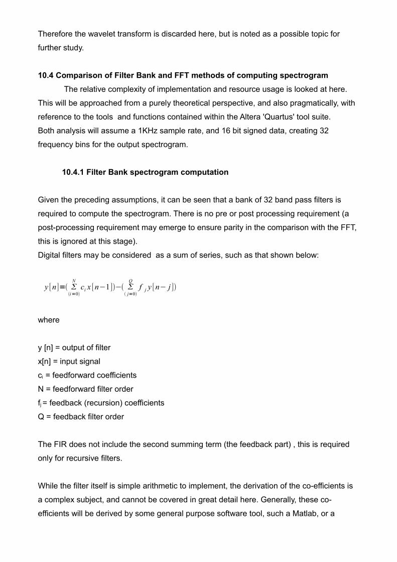
10.4.1 Filter Bank spectrogram computation
Given the preceding assumptions, it can be seen that a bank of 32 band pass filters is
required to compute the spectrogram. There is no pre or post processing requirement (a
post-processing requirement may emerge to ensure parity in the comparison with the FFT,
this is ignored at this stage).
Digital filters may be considered as a sum of series, such as that shown below:
y [n]= i=0
N
ci x [n−1]− j=0
Q
f j y [n− j ]
where
y [n] = output of filter
x[n] = input signal
ci = feedforward coefficients
N = feedforward filter order
fj = feedback (recursion) coefficients
Q = feedback filter order
The FIR does not include the second summing term (the feedback part) , this is required
only for recursive filters.
While the filter itself is simple arithmetic to implement, the derivation of the co-efficients is
a complex subject, and cannot be covered in great detail here. Generally, these co-
efficients will be derived by some general purpose software tool, such a Matlab, or a

dedicated programme or applet . Initial work was done iteratively with the authors tool,
'sincfilter' and also 'fiview' (Jim Peters) to gain a feel for filter requirements. Tools for
designing digital filters are also to be found within many digital design packages. In
particular, the Quartus suite that is used in this project provides a 'wizard' to define FIR
filter coefficients, and even provides the code to implement them.
Since this tool is optimised for FPGA applications, it is appropriate to use this for
evaluation.
It was stated previously that the filter bank here would require 32 filters. Assuming a
linear distribution of frequency bins, and that they are confined to the range 0 to 500Hz
(Nyquist criteria sets upper limit to ½ sample frequency, in this case 1KHz).
Ideally each filter is to be some 500/32 = 15.635Hz wide, however, in practice, there will
be some compromises in the design. Some overlap is assumed, either in the pass band
itself, or in the filter response skirts.
For this evaluation then, based on the above requirement, The Quartus tool was
used to create FIR band pass filters centred around 16Hz. These were iteratively shown to
require around 64 coefficients, each of 16 bits. This filter would therefore require 64
multipliers and 64 adders. While the adders can be more or less disregarded in terms of
FPGA resource, the multipliers cannot. When it is considered that 32 such filters would be
required, a total of 2048 multipliers is indicated.
This would give rise to a completely parralelised solution, with filter outputs being
valid almost immediately after the most recent sample presented (assuming combinatorial
multipliers, the delay is simply the propagation times.) . This performance would far
outweigh any requirement, the notional sample rate is 1KHz, but an FPGA may be clocked
in the tens , even hundreds of MHz. In fact the development system currently targeted has
a 50MHz clock on board, (faster clocks may be generated by the PLL). Taking the 50MHz
clock as standard rate, then there are 50,000 processing cycles available for every data
sample taken. This would seem to indicate that a heavily pipelined and multiplexed system
could vastly reduce the hardware overhead, to the extent that a single hardware multiplier
would be capable of fulfilling the whole process (2048 multiplications in 50,000 cycles,
readily achievable). However, it is would seem that the control systems to achieve this
would be complex, possibly beyond the scope of this project. It is noted that for a real,
commercial product, this sort of effort would be essential to ensure a cost effective system.
It is suggested that, if a filter system is attempted for this project, a compromise is likely ,
where a single 'generic' filter is used to generate in turn each of the 32 frequency bins.

This still leaves a need for around 32 multipliers, but is somewhat more manageable.
Retaining some level of paralleling also has the benefit of leaving some headroom should
there be some subsequent need to increase the sample rate.
The filter bank method also requires 4096 bytes of ram (32*64*16bit) to store the co-
efficients.
For the purpose of comparison with the FFT method of computing the spectrogram, the
following assertions are made
1) Filter bank requires 32 multipliers (but conceivably 1 multiplier)
2) Filter bank requires 4096 Bytes of persistent storage
3) Filter bank has no pre or post processing requirements
Additionally, it is stated that the filter bank method requires some work (determining co-
efficients) before any implementation code can commence. The filter bank as above will
require some sort of relatively complex controller.
10.4.2 FFT Spectrogram computation
It was stated that of special interest is the Short Time FFT. This has a number of
pre-processing requirements ,the data is broken into segments, and each segment is
passed through a 'window' than can be thought of as 'smoothing off' the edges of the data
set in that segment.
An additional requirement, that the segments overlap is not compulsory, but is
chosen for this application, to give better temporal resolution to any spectral features.
Additionally, there is a post processing requirement with the FFT, in that it outputs complex
data (complex as in two terms, a real and imaginary part, not complex as in complicated).
These need to be 'reassembled' into a magnitude. The angle, (phase information) is
discarded.
A complete, ground up design of an FFT would be beyond the scope of this project.
Fortunately, the Altera design software provides an FFT 'IP Core ' that is free to use for
evaluation purposes.
The interface to the FFT is relatively simple, and is a standard across many of Altera's IP
cores. The resource usage of an FFT of certain sizes can be readily looked up in Altera's
documentation.
This is describing an FFT with16 bit data, implemented with four multipliers.

The parameters of this (64 point, 16 bit) do not appear in the table, so the resource
usage is estimated here.
There are four multipliers (by definition in this design), and 9792 bits of memory (=
1224 bytes ) (taking the figure for 256 points and divide by four. This was 'sanity checked'
against the other entries and was seen to hold true)
For the purposes of comparison, the following assertions are made
1) The FFT uses four multipliers
2) The FFT requires 1224 Bytes of memory
3) The FFT requires an additional memory, in the order of 128 bytes, as an
input buffer
4) The FFT requires post and pre-processing.
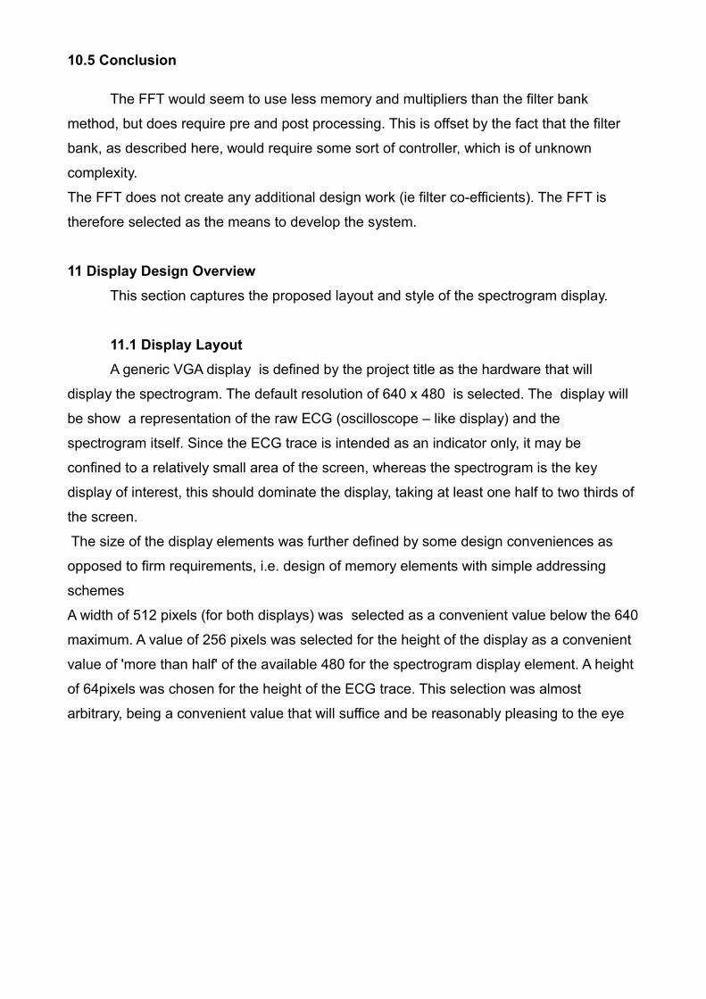
10.5 Conclusion
The FFT would seem to use less memory and multipliers than the filter bank
method, but does require pre and post processing. This is offset by the fact that the filter
bank, as described here, would require some sort of controller, which is of unknown
complexity.
The FFT does not create any additional design work (ie filter co-efficients). The FFT is
therefore selected as the means to develop the system.
11 Display Design Overview
This section captures the proposed layout and style of the spectrogram display.
11.1 Display Layout
A generic VGA display is defined by the project title as the hardware that will
display the spectrogram. The default resolution of 640 x 480 is selected. The display will
be show a representation of the raw ECG (oscilloscope – like display) and the
spectrogram itself. Since the ECG trace is intended as an indicator only, it may be
confined to a relatively small area of the screen, whereas the spectrogram is the key
display of interest, this should dominate the display, taking at least one half to two thirds of
the screen.
The size of the display elements was further defined by some design conveniences as
opposed to firm requirements, i.e. design of memory elements with simple addressing
schemes
A width of 512 pixels (for both displays) was selected as a convenient value below the 640
maximum. A value of 256 pixels was selected for the height of the display as a convenient
value of 'more than half' of the available 480 for the spectrogram display element. A height
of 64pixels was chosen for the height of the ECG trace. This selection was almost
arbitrary, being a convenient value that will suffice and be reasonably pleasing to the eye

These display boxes are to be centralised about the x-axis, and distributed approximately
as per sketch below
11.2 Spectrogram display format
Spectrogram are generally displayed in either of two ways. A '3D' spectrogram
creates a 'landscape' out of successive spectra. This can be shown as a 'wire-frame' or as
a surface.
An example is given below.
Display region for spectrogram
Display region for ECG raw trace
Fig 11.1

Where in this case each spectrum is a trace, offset in the y-axis. Note that this has
to have some perspective applied to distinguish the traces.
An alternative means to present the spectrogram is to use present it as a flat xy
plot, where x represents time, y represents frequency, and the magnitude of any given
point is given by pixel colour (reminiscent of thermal imaging cameras) or as a
monochrome/greyscale. An example is given below.
http://en.wikipedia.org/wiki/File:Spectrogram-19thC.png (under creative commons)
Of these possibilities, the 3D representation is the most striking, but not perhaps the
most representative. Further to this, the 3D display would require some substantial post
processing. The 2D display is therefore easier to implement, and also perhaps more
appropriate.
The ECG trace presents less of a challenge, only a single bit is required per data
point, as this is to all intents and purposes an 'oscilloscope' type display
The actual memory requirements are somewhat lower than they might first appear,
the current proposed FFT results in 32 useable frequency 'bins' and there are currently
proposed 256 slots per 'screenful' giving a total requirement for the display of 8K by 8 bits
(=64K bits for the spectrogram. The ECG trace is 512x64x1 = 32K bits
At this stage, no text legend is proposed for the display, however it is intended to
have some sort of graticule/grid (not shown on sketch) to enable identification of

ECG DisplayElement
Sync and counterGeneration, and
Display multiplex
Red (0..3)
Green (0..3)
Blue (0..3)
Red
HSync
VSync
HCount
VCount
Spec_Red (0..3)
Spec_Green (0..3)
ECG_Red (0..3)
ECG_Green (0..3)
ECG_Blue (0..3)
Spec_Blue (0..3)
Spec_Valid
ECG_Valid
SpectrogramDisplay Element
'Rest of system'Interface TBD
PLLVGA Clock
DACs Green
Blue
27MHz
V
GA
Con
nect
orFPGA
Dev Board
frequencies and temporal correlation of spectrogram and ECG.
12 Design activity log – Display
12.1 Display System Block Diagram
The block diagram, below, indicates the intended architecture of the display
system.The Spectrogram and ECG display elements are substantially memory areas with
custom interfaces to translate the horizontal and vertical position of the VGA scan into
addresses, along with other control line to the rest of the system.
The larger, central block 'Sync and counter generation' is the core of the low level
VGA driver. The DAC's are, on this board, simple resistor ladders, so no further detail is
given here, other than to note that they are limited to 4 bits wide each.
12.2 Low level VGA driver
The external VGA interface has 5 signals
Fig 12.1

Red (analogue),Green (analogue),Blue (analogue)
Horizontal Sync (digital),2 Vertical Sync (digital)
The three colours are each derived from a 4bit resistor ladder DAC on the
development board, giving a maximum, theoretical, possible 12 bit colour resolution.
The horizontal and vertical sync pulses, and their generation, are defined and designed for
below.
12.2.1 Horizontal Synch pulse
Horizontal sync defines the window in which a row of pixels is written to the
monitor. A typical horizontal sync pulse, for a 60Hz refresh rate is given below
The 'porches' provide for some framing for the actual data.
Given that the data period of 25.17us represents 640 'ticks' of the master clock, it is
relatively straight forward to derive the clock frequency as 1/(25.17us/640) = 25.427MHz.
This may be noted to differ slightly from some published values (eg
http://en.wikipedia.org/wiki/Video_Graphics_Array and
http://www.ami.ac.uk/courses/ami4460_fpga/restricted/designexercises/de5/index.asp
) both of these sources quoting 25.175MHz. In practice this will not matter a great deal,
there may be a small impact on number of pixels per row, and a negligible impact on the
refresh rate.
Since the Development Board does not have a 25.427 MHz (or indeed a 25.175MHz)
clock source, one must be created. The FPGA device does have Phase Locked Loop
(PLL) circuitry available to facilitate this. This is beyond the scope of this section, and will
be covered under code generation
3.77us 1.89us 25.17us0.94us
31.77us
Active RGB dataFrontPorch
RearPorch
Fig xxx Horizontal Sync Pulse Timing

This clock will be used to drive a counter having around 807 steps* and the value
of that counter directly correlates to the state of the sync pulse.
*(Derived by dividing the 640 pixels by the 25.17us they occupy, and multiplying by the 31.77us that the entire row occupies
(640/25.17)*31.77 = 807.81
Let us assume that to simplify the memory interface, that when the counter is zero, this
corresponds to the first pixel in that row, then we have
Count Value Description/Action State of pulse
0 – 639 Directly addressing memory, colour data present High
640 - 660 Rear Porch High
661-756 Synchronisation pulse Low
757-808 Front Porch High
It is stated here that while it was attempted to derive exact values, these values given
above are approximate/notional, and subject to change during development.
Since internally the system does not need to be aware of the porches, the physical
implementation of the horizontal synch signal simplifies to:
“Horizontal synch is always high, except when the counter is between 660 and 757”
The value of the count will be made available to other elements in the system.
12.2.2 Vertical Synch pulse
The vertical synch defines an actual frame, or 'screenful' of display. It has much the
same structure as the horizontal synch, but is considerably slower, its active region
encompassing 480 lines .
The vertical synch will therefore be derived from a counter in a similar manner to the
horizontal synch. A typical timing diagram for the vertical synch is given below,
64us 1.02ms 15.24ms0.35ms
16.6ms
480 rows at 31.77us ea =(15.24ms)
FrontPorch
RearPorch
Fig xxx Vertical Sync Pulse Timing

The Vsync counter will be incremented at the end of each horizontal scan, and not be
cleared until after it presents a rear porch after the 480th row has been completed
Taking the timings given above, and with the same caveat as with horizontal synch , a
table is presented below indicating the relationship betveen the count value and the action
and state of the sync line. Where there is a dependency on the Hsync, this is indicated
Vcount Hcount* Description State
0 - 479 all Window in which rows being clocked to display High
480 - 491 n/a Rear porch High
491 - 493 n/a Sync pulse, end of screen Low
493-525 n/a Front porch, High
525 756-808 Vertical counter cleared High*It is given that Vcount increments when Hcount = 808, so this dependency is omitted
As with the horizontal sync, no intelligence is required about the porches , so the physical
implementation of the vertical sync can be summed up
“Vertical Synch is always high except when counter is between 491 and 493”
As with the horizontal sync, the count value will be made available to the rest of the
system for addressing purposes.
If the counters are generating the physical signals for Horizontal sync and Vertical sync it
seems reasonable to include the RGB data in the output of the same entity, and hence this
will need the RGB from each of the display elements (spectrogram and ecg) and deal with
multiplexing these with each other and any other features (border colour, graticule,legend,
etc).
This then allows definition of the interface as below .Global clocks and resets are not
shown below.

12.2.3 Integration and verification of Synch Pulse generators
With reference to block diagram in section 12.1, The block titled 'Sync and counter
generation, and display multiplex ' is coded in the file VgaCountersAndMux.vhd within
the 'TopLayer' project , up to and including Rev 18 of that project is compliant with the
interface described above.
It is at this point noted that the interface is perhaps a little cumbersome, there are two sets
of RGB buses, and two control lines to the sync pulse generator. A better architecture may
be to put a wrapper around the display elements to handle the mux'ing etc, however, at
this stage the design process will proceed as is, with any improvements reserved for a
later implementation stage
This was simulated (but note that the PLL was emulated in code, not actually instantiated
for simulation purposes) Simulation was not performed at any great depth at this stage,
just sufficient to demonstrate that basic behavior appears correct
ECG DisplayElement
Sync and counterGeneration, and
Display multiplex
Red (0..3)
Green (0..3)
Blue (0..3)
Red
HSync
VSync
HCount
VCount
Spec_Red (0..3)
Spec_Green (0..3)
ECG_Red (0..3)
ECG_Green (0..3)
ECG_Blue (0..3)
Spec_Blue (0..3)
Spec_Valid
ECG_Valid
SpectrogramDisplay Element
'Rest of system'Interface TBD
PLLVGA Clock
DACs Green
Blue
27MHz
V
GA
Con
nect
or
FPGA
Dev Board

Note that with all these simulations, a correction is applied to some of the timing
measurement where there is an inconsistency with the time step used by the test bench
and 'real world' time
showing two consecutive falling edges of the Hsync pulse
Note : Time of 32000000pS (32us) as the test bench uses precisely 40ns period for the
PLL clock (25MHz) , normalising this with a correction factor of 25/25.175 does yield
31.7775us which is consistent with the target period.
two consecutive falling edges of Vsync
showing a time of 16800000000ps (16.8ms),applying the same correction factor of
25/25.175 yields
16.683ms, consistent with value defined earlier for the period of the Vsync pulse

Verify falling edge of H sync
Here, the horizontal sync can be seen to have its falling edge at the count of 661, as
intended. The rising edge was seen to be at count of 757, which was also correct.
Similar checks, not documented here, were performed on the relationship between the
Vsync line and the counters, these were found to be compliant with the requirements
defined earlier.
12.3 Generic Display Element
Design was then to commence on the two display elements. With the interface to
the VgaCountersAndMux entity already defined, it was necessary to consider how the
display elements will interact with the rest of the system (maths block). The simplest
possible interface would be to simply 'strobe in' the data in the order that it comes out of
the maths block. This was adopted, but with the additional refinement of a 'column finished
' signal to provide a means for the memory addressing scheme to re-synchronise if (e.g)
there is some delay in the math block, and to ensure scrolling occurs reliably. A reset (in
addition to the global system reset) was provisioned for, to enable the maths block or
some other part of the rest of the system to reset these elements. This reset was not
implemented at this point, merely provisioned for.
Both elements are virtually identical at a high level view, and so a generic
description of their features and development is given here, and a generic interface is
shown (substitute 'Scope' or 'Spectrum' for X in the drawings below.) Global clocks and
resets are not shown

The core of the display elements is a dual port memory. Initially, the circular buffer
developed for the maths block was considered, however the Quartus software does
provide a dual port memory entity that is freely useable.
As the maths block make data available, the values are written into the memory. As
each item of data is strobed in, the low order write address is incremented. The strobe is
directly used to enable writing to the memory element.
When a packet (either a frames worth from the FFT or a certain number of ECG points)
have been been presented, the maths block issues a 'sweep', in other words one of these
packets represents a column of display data. The 'sweep' is used by the display element to
a) increment(or decrement!) the high order write address
b) scroll the display one column
The read address is derived from the Hcount and Vcount signals provided by
VgaCountersAndMux entity. As there are more pixels in the display area than there are
memory locations, some of the low order bits of the count values are discarded prior to
them being merged.
Some of the highest order bits from Hcount form the low order bits of the read address,
and some highest order bits of Vcount form the high order bits of the read address (it
was not compulsory to design it so, it was implemented this way to ensure efficient use of
memory.)
The display element has, hard coded into it, a definition of the screen area it fills.
This definition is in terms of the Hcount and Vcount values, when these are within certain
limits, the display element asserts its 'display valid' signal, which in turn informs
XDisplayBox
Horizontal
Vertical
XRedOut
XGreenOut
XBlueOut
XColourValid
XAmplitude
XStrobe
XSweep
XReset

VgaCountersAndMux which RGB data to forward to the DACS and hence display.
Two such elements were coded for, and are named ScopeDisplayBox.vhd and
SpectrumDisplayBox.vhd . Some functional differences exist between these entities.
ScopeDisplayBox displays a single, pixel for each data point, whereas
SpectrumDisplayBox must convert the input value to some colour based representation of
magnitude. In this instance, a simple scheme is implemented that assigns different bitfields
of the magnitude to each of the RGB registers. While this is a crude method, and
somewhat difficult to interpret, it is memory and resource efficient. For the purpose of
system level testing, all that is required is to provide a level of discrimination. It is
anticipated that this will be re-visited at later date, either within the project or as research
after.
Versions of this code at R18 are compliant with the interface described. These were
not simulated at this stage, deferring verification until a data source is available
12.4 Integration of display elements and low level driver
With the main elements designed and verified, a functional test was to be
designed.
Two new entities, ScopeEmulator and SpectrumEmulator were designed to read some
hard coded data embedded within them, and place the data on an interface compliant with
that defined for the display elements. These were each coded as two process state
machines. (one synchronous, the other asynchronous.)
Both were simulated and verified . As they are nearly identical, only simulation results for
'SpectrumEmulator , are presented here.

The annotated plot correctly shows the intended behavior, 32 amplitudes are strobed out,
followed by a 'sweep' pulse that is used to trigger the scroll of the display.
12.5 Integration tests and demonstration
These entities were then placed in a wrapper entity 'SystemEmulator' This was
placed in the project 'TopLayer” , within which the display elements were also included,
along with appropriate interconnect signals within the entities and ports to the outside
world.
Pin assignments were made , and the full project built, the device programmed.
This was not an immediate success, the ECG trace was inverted, and the spectrogram
was not in phase with the ECG. Both of these were relatively easy to debug (a numerical
error in the delay in the state machine of the SpectrumEmulator entity, and a sign error in
the ScopeDisplayBox entity.
These changes are captured in R19 of the 'TopLevel' project,
This was then re-built, and functioned satisfactorily. The Hold button was
implemented on KEY1 of the dev board, and functioned, correctly a screen shot of the
display is shown below. Note that the data is emulated, hence, particularly with the
spectrogram, it is clearly a repeating pattern.

A popular video streaming site was used to host a demonstration of the display
scrolling, may be found at the following URL: http://youtu.be/fYCHteqULuE
13 Design of Spectrogram computation.
13.1 Spectrogram computation high level design
Having now completed a means of displaying the data, attention now returns to the
generation of the spectrogram, the design of the part that has generally been referred to
as the 'maths block'.
The input side of the maths block interface needs to comprise of an input stream for
the ECG sample data, and the global clock and reset. Some additional handshaking will be
provisioned for, a means for the data source to assert that data is valid, and a means for
the math block to assert that it is ready. It may not be necessary to implement this
handshaking, but it is provisioned for
The Maths block has several functions. Based on the current model of an STFFT to

Hold
ECGDataIn
ECGDataStrobe
MathReady
SpecAmplitude
SpecStrobe
SpecSweep
SpecReset
ScopeAmplitude
ScopeStrobe
ScopeSweep
ScopeReset
To the display sub system
Fifo(circular buffer)
WindowFunction FFT
Post -Process
Maths Block
create the spectrogram, it must:
1 Buffer the incoming data and Manage the data into 'slices'
3 Pre-process the data (apply windowing function)
4 Manage interface to the FFT block
5 Manage data out of FFT block
6 Post process data out of FFT block,
7 Manage data to the two display interfaces
13.1.1 Block Diagram
The diagram below gives some system level indication of the entities that will be
created, and the interfaces required.

13.2 Description of items in block diagram
Each of the subentities in fig 13.1.1 are discussed in turn, below, and the basis for
detailed design and coding laid down.
13.2.1 FIFO (circular buffer)
This block buffers the incoming data and manage into 'slices' . This is to fulfill the
requirement to sequentially present 'overlapping slices' of the data to the spectrogram
generator.
13.2.2 Window Function
The FFT as used in this system is considered to be of short duration (containing only 10's,
rather than 100's or 1000's of sample). This tends to lead to some spurious outputs,
referred to as spectral leakage. A common mitigation for this is to pass the input through a
'window' which attenuates the samples at the beginning and end of the data slice, reducing
the contribution these make. There are a number of functions suggested for this. For this
project, a curve known as the 'Hann Function' is selected.
13.2.3 FFT
The FFT itself, as currently defined is a piece of Altera Intellectual Property, a feature
provided by the development software. This is freely provided for demonstration and
evaluation purposes, subject to certain usage restrictions. It would be expected that for a
commercial product, a FFT would be developed 'in house' as there would be opportunities
for application specific optimizations. For this project, however, use of the IP is
appropriate.
This does require that the interface to it is compliant with a proprietary standard known as
“Avalon “ . The FFT block as shown in fig qqq does include the Avalon interface and any
additional control needed.
13.2.4 Post Process
The results from the FFT block are the real and imaginary components of complex
numbers. These need to be combined, to create a single magnitude value. This may be
achieved trigonometrically or arithmetically, or even by look up table. Since there is a large
difference between the main system clock (50MHz) and the data rate (TBD, but is 10's of

Khz) there are plenty of cycles available to do the processing without recourse to piplining
schemes. The phase information that is also encoded in the complex numbers is not
required in this application, so is not processed.
The output of the FFT magnitude plot it symmetrical, so half of the output data can be
discarded.
13.3 Management of data from the maths block to display interfaces
The FFT post processing entity is to be designed in such a way as for it to simply clock it's
output to the SpectrumDisplay entity.
The ECG raw trace needs a little more management. While it is passed unprocessed to
the 'ScopeDisplay' entity, it must be gated somewhat, recalling the slicing of the input data
(i.e. the overlapping) the raw ECG data is transferred at ¼ of the rate of the FFT outputs.
This remains to be decided at this stage, and will be dealt with at a fairly late stage of
integration, after all the main entities have been designed and tested.
While the interfaces to and from the Maths block appear relatively simple, there will
be a significant number of entities involved.
13.4 Design of sub entities in 'Math Block'
13.4.1 Note on change of resolution.
It should be noted at this point that a decision has been made to do this initial
design work at a lower resolution that as determined in the earlier section 'Derivation of
Hardware requirements for spectrogram capture' ;
Sample Rate 1Khz
Sample Size 8 Bits
FFT Size 64 Samples
The purpose for this quite drastic reduction is to ensure that a build of the entire system is
actually possible within the available resource of the device selected. Resolutions may be
scaled up when a working system has been built and tested.
A fairly ' middle out' approach was taken for the implementation of these entities, starting
with the FFT block, moving 'left' through the pre-processor and buffer/slicer entity, before
completing the post-processing feature , and 'hand off' to the display system itself. The
means of obtaining raw ECG data is beyond the scope of this section, but is returned to
later or something .

13.4.2 Design and test of FFT controller.
Prior to designing and testing the FFT controller, it was decided to verify the
behavior of the FFT block in isolation. This is documented here, prior to discussing the
controller. The purpose of this is to ensure that when the controller itself is developed,
there is confidence in the FFT block.
A spreadsheet (FourSines.ods, attached with electronic copies of this dissertation, or
downloadable from www.peterbrewster.co.uk) was used to construct a signal composed of
four well defined frequencies fractions of the sample rate, namely 1/256, 1/64, 1/16 and
1/8 converted into suitable 16 bit values for the FFT block test bench.These formed the
real input to the FFT. This was plotted for visual verification, however, a detailed analysis
of the spreadsheet data is recommended if the reader wishes close inspection of the
validity of the signal.
The FFT also expects an imaginary input, these were set to zero.
The FFT tests were run, and the real and imaginary outputs imported to the same
spreadsheet to be combined into a magnitude plot for analysis. The spreadsheet was used
to create a plot of this (below) . This is provides an excellent result, there are four distinct
peaks, located in the correct positions for the frequencies they represent.

The plot is shown at close up, much of the output has been discarded, as the FFT output
exhibits symmetery, i.e. repeats the data as a 'reflection' around the centre of the x-axis.
Given the strength of this result, the controller could be designed with confidence.
Initially the FFT controller seemed to be difficult to implement, given that it is a piece
of vendor IP with the proprietary 'Avalon' interface. However, once the naming
conventions and timings were understood, it resolved itself as a fairly trivial problem.
Two entities, 'FFTSourceController.vhd' and 'FFTSinkController.vhd' were created.
The naming of the sink and source controllers reflect the functionality with respect to the
Avalon interface, from the perspective of the FFT block, ie
the sink controller manages data to the FFT,
the source controller manages data from the FFT to the post-processor.
Both of these entities where then instantiated in a wrapper function ' FFTController.vhd '.
The FFTController entity also instantiated the FFT itself.
During debug, of particular note was a feature of the FFT block Avalon interface, that if it
is not informed that there is no error detected by the sink controller, it seems to assume
that there is one, and remains quite inert. This did not appear to be documented in the
user guides to hand, however this may no longer be the case for later release. This is
mentioned here as this did cause a delay until the error was found. In this application, this
is not an issue in itself, and was resolved simply by tying the relevant lines to logic 0.
Initial simulation showed the interface to be functioning correctly.

13.4.3 Design and test of Preprocessor.
The preprocessor has two functions, the 'windowing' and the buffering and 'slicing' .
These are discussed in turn, here.
13.4.3.1 Design of window function
As previously indicated, the input data is multiplied by a corresponding Co-efficient in the
'Hann Function'
The Hann function is given by Co-efficient(n) = sin2(πn/(N-1)
(where N = number of samples in window/length of table)
The effect of the function, to attenuate the first and last samples in the input data can be
visualised when they are plotted, as below.
A spread sheet, hannfunction_arrayMaker.ods (distributed with electronic copies of , or
downloadable from www.peterbrewster.co.uk ) was used to create the LUT entries, and
present them in a format that could be pasted directly into VHDL as an array.
To preserve resolution, the values were scaled by a factor of 1024 before being imported
to the code.
The wrapper for the function was relatively simple, consisting of two processes, one
managing the clocking in and out of the data, and tracking which member of the LUT to
apply, and the other actually applying the factor, and scaling the result back down.
Initial simulation demonstrated the overall behavior appeared correct . Further testing
using fixed/controlled inputs was performed, a plot of one such simulation is given below.
This was tested and simulated. This is not evidenced here, as a subsequent refactoring
permitted this function to be absorbed by the next entity to be designed, described below.
0.00000000
0.20000000
0.40000000
0.60000000
0.80000000
1.00000000
1.20000000
Hann Function
n
Co
-eff
icie
nt

13.4.3.2 Design of Buffer and 'Slicer'
The function of this block is to buffer the data, and present it to the FFT block (via the
window function, described above) in packets of the appropriate size. In addition to that, it
also ensures that the packets have the 'overlap' required to improve the temporal
localization of any spectral features, as, discussed in section blab of the system level
design specification.
The Buffer was designed around a dual port ram 'megafunction'
The write address register of the Dual Port Ram was automatically incremented on every
ECG_Clock. The Read Address register was also similarly incremented, but also, on every
64th data input , the Read Address Register has a negative offset of 48 applied to achieve
the overlap requirement. As indicated previously, the application of the Hann function was
subsequently moved into this entity in an attempt to simplify the system level design.
Simulation, below, shows the output of the buffer, application of Hann function evidenced
by the fixed input giving an output that rises and falls over the correct window length.
13.4.4 Design of post processor
Given than all of the substantial 'input side' blocks are now complete to a viable state
(leaving aside the acquisition of raw data) it was decided to proceed with design of the
post processor, as the data acquisition may be emulated by some digital (e.g. serial port) .
With the post processor complete, it will then be possible to attempt to move to a system
integration phase
There is a further element required in the output stages, a buffer/delay to forward the raw
data to the 'oscilloscope' display. While this is expected to be relatively trivial, it is noted
here as required, to be dealt with at some late integration stage.

The purpose of the post processor has already been given. In this implementation,
the calculation is performed by what amounts to Pythagoras' theorem, by treating the real
and imaginary parts as two sides of a right angled triangle, the result being the
hypotenuse. This method is appropriate here because of the relatively small word length,
and the inherent guarantee (in the way the FFT block functions) that they have the same
exponent. A further feature of this system that lends itself to such a relatively simple
solution is that the data is very slow with respect to the fastest clock available. This permits
a multi-stage method that does not rely on any complex pipeline schemes.
The post processor therefore needs a means of finding the squares and square
roots of the data.
Squaring is considered trivial in this case, as a multiply function will suffice. This can be
achieved with a combinatorial solution, and may be implemented on a 'one per' basis, or
as a process that is re-used. In this case, it was decided to use a single multiplier and re
use this. These are considered relatively trivial and will not be discussed in further detail
until the final 'post processor,' has been implemented,
Taking the square root (of the 'square of the hypotenuse' ) was initially viewed as a difficult
problem, however it soon yielded to research, in particular the paper “A New Non-
Restoring Square Root Algorithm and its VLSI Implementation “ (Li and Chu, University of
Aizu, Japan, 1996) was studied.
While the method presented in that text was not used, it was that paper's
discussion on earlier methods that gave the insight- the relatively short bit length of the
numbers in question meant that there was no real reward (in clock cycles) for
implementing a complex algorithm.
The radicand is the sum of two squares, both of which have, as discussed, the same
exponent. The practical benefit of this is that the exponent does not need to be
considered, the square of the mantissa is found, and the exponent is simply ignored and
re-applied unchanged to the final answer.
The selected algorithm is quite simple, starting with a seed value, it progressively sets bits
(starting from most significant to least) and testing at each iteration if the square of this
new value (multiplied by itself )is equal, less than, or greater than , the radicand. This
therefore takes as many iterations as half the number of bits in the square.
This was implemented over two source files, SquareRoot.vhd and RootIterator.vhd .

RootIterator performs the multiplication and comparison functions, returning a flag to set or
clear the relevant bit in the accumulator (and a 'finish' flag just in case it finds a perfect
square quite quickly) RootIterator has no knowledge of the state of the whole calculation.
SquareRoot manages the setting of the bits, and compiles the result.
The code was not written to be (clock ) cycle efficient, it was written in such a style as to
permit simulation to view the system at every stage, and study its operation in detail, as it
was identified as something worthy of study in isolation
Some potential efficiencies were identified, for example, finding the first bit set in the
radicand would permit the solution to be commenced a number of iterations along the
sequence (i.e. omission of leading zeros) . Again, for the relatively small numbers that are
being used here, the reward would be small, possibly even negative.
The SquareRoot function was simulated in isolation to the rest of the post processor. It
can be seen to be accurate to 1 LSB. Simulation capture presented here
It can be seen that the function will always round down (in the absence of a perfect
square). It may be possible to mitigate for this by shifting the radicand a multiple of two
places to the left, and correcting at the end, however, given that the maximum error stands
at -1LSB, this will not be considered further.
The square root was instantiated in the post processing entity. Since this is
mathematically equivalent to applying Pythagoras theorem , (taking the root of the sum of
two squares) the entity was named Samos.vhd, after the island where Pythagoras was
born.
The post processor was simulated and seen to function as predicted, plot inserted below,

Amongst the test data, the encircled examples provide verification that is easily
recognizable to any who recall their elementary trigonometry, the “3,4,5” and “5,12,13”
triangles. Closer attention to the other results does also indicate the function operates
correctly, and that it exhibits the maximum error of -1 LSB, inherited from the square root
function.
This then completes the substantial part of the design , there will be some need for 'glue
logic' in the implementation phase, this will be developed as this progresses.
13.5 Integration and test of elements
A low level block diagram is given here, based on the source code. It is not a
system diagram as such, it is presented to show how the code is built, and which element
intantiates which other elements. Some very lowest level objects , some memory items
and a PLL clock source are not shown, however these are compiler generated items, not
handwritten code for the project.

Before any integration can take place, an oversight must be addressed.
The feature that creates the overlapping of the slices does mean that the FFT will not, as
the design stands, be consuming data as fast as it is being presented, by a factor of four.
It is not proposed to remove the overlapping, as this contributes to the value of the system.
Instead, a clock at four times the sample rate will be derived from the 50MHz clock, and
used to drive the FFT. This was implemented in 'ClockGen.vhd' .
This is considered a relatively trivial matter, so will not be considered further here.
There is also an outstanding issue, in that there is a lag between the start of data being
loaded into the FFT core, and valid data coming out. Simulations show this to be some
168 clock cycles. While for the output FFT output data this is of no concern, as the FFT
behaves as a buffer for the output, there will be some loss of synchronisation between the
SpectrumDisplayBox.vhd
VgaCountersAndMux.vhd
ScopeDisplayBox.vhd
DisplaySystem.vhd
SystemWrapper.vhd
ClockGen.vhd
ScopeSource.vhd
RootIterator.vhd
Samos.vhd
SquareRoot.vhd
SliceBuffer.vhd
SpectrumGenerator.vhd
FFTController.vhd
FFTSourceController.vhd
FFTBlock.vhd
FFTSinkController.vhd

raw data (the 'scope' like trace) and the ECG. In the interim, the raw data display will be
disabled, but it is noted that the resolution to this would be to introduce a FIFO buffer, of
sufficient length to accommodate this delay. This would then simply be enabled once the
FFT signals the start of valid data output.
Initial integration builds would use an emulated data source, much as was used in the
display system tests. An entity named 'ScopeSource.vhd' was created. This permitted the
system to be developed virtually to completion without the distraction of creating an
interface to some other hardware. That will be left as time permits.
A branch of the earlier code was made, and pulled into a project named
'SystemWrapper.qpf'
This was built and programmed on to the device. The image was consistent with a low
resolution spectrogram. This was captured and placed on the video streaming site at the
following URL http://www.youtube.com/watch?v=pW_UyI5mOwg
That test caught an error in the system, in that both 'halves' of the FFT output had been
used in the computation of the spectrogram. This was readily corrected by implementing a
spare signal on the interface from the FFTController entity .In addition the waveform in the
'ScopeSource' entity was modified to be more periodic, with approximately 16 cycles per
64 samples. This would give strong output in the frequency bins around (slightly over) ¼ of
the sample frequency.
The system was rebuilt and re-programmed. A screenshot of that output is shown below

This more closely resembles a spectrogram. The high density of coloured pixels in
the upper middle half to correlates to the ¼ sample rate suggested (the top of the screen
representing nyquist limit of ½ the sample frequency.)
This does now indicate a new ,introduced weakness in the system. When the use of
the 'upper half' of the spectrogram was fixed, no steps were taken to then use up the 'dead
space' on the display. To do so would double the (visual) dynamic range of the system.
This would represent a disruptive change to the code base at a late stage in the project,
and hence is left as-is.
It was noted in Section 12.3 that a quite crude method of creating a colour
representation of the magnitude was used. A typical 'thermal image' type of representation
would have the lower magnitudes in blue,moving through shades of green, to red, and
yellow , before using white as the greatest magnitude. While this scheme is not inherently
correct, it would seem to be an ideal output format as it is more likely to be intuitively
grasped by the user. At this stage, the arithmetic transform to implement this will not be
atttempted, however it will be disscussed in further detail in section 15, (Conclusions and
Suggested further work). A compromise was built, whereby, at the cost of large part of the
resolution, a grey scale where each of the RGB registers is set to the same value, derived
from the upper 4 bits of the spectrogram data. A screen shot of this is given below.
Design activity ceases here for the purpose of this project. The next section presents
conclusions and indicates areas of further design work and study.

15 Conclusions and Suggested further work
The concept of a spectrogram display system on an FPGA was evaluated, in terms
of usefulness and possible commercial viability. There was mixed findings as to
commercial viability of the system in the original stated application, however the overall
balance would seem to support the view that this technology would be a contender for the
most cost-effective solution should a real demand exist. This is also mitigated by the fact
that a number of other potential applications were readily identified. Other issues around
product realisation were looked at. An outline functional specification was created, and
agency requirements had some cursory study.
A system level design was raised, and hardware requirements derived. A further,
highly detailed and somewhat idealised system was designed. This covered the full 'end to
end system' from audio level input to VGA output.
Based upon a subset of this design, functional blocks were coded in VHDL. These
did not encompass the entire scope of the detailed design, a system with emulated input
was designed. These blocks where verified by simulation, and seen to behave correctly in
isolation. The blocks were integrated into full system, built, and a device programmed. An
appropriate output was viewed on the VGA monitor.
While the system did function as intended, there are a number of areas of that would
benefit from further work.
1) Greater resolution of output display
2) Improvements to readability/aesthetics of display
3) 'Real' (not emulated) data interface.
4) Data Capture
Each of these is now discussed it turn.
15.1 Greater Resolution of output display
It is perhaps self evident to say that an increased level of detail on the display makes the
system inherently more useful. To make any significant change would require greater
memory made available as display RAM . The resource usage of the final build did not
permit significant increases in memory to be made available, and moving to a larger
device is not a cost effective solution. It is proposed that external memory devices are
used as display ram (this was referred to, somewhat obliquely, in section 6.2.6, some
rough budgetary costings for the system indicated use of DDR memory). This would

require the creation of a driver to emulate Dual Port memory – so the spectrogram
generator could write to it while the VGA block read from it. It is suggested that this is
achieved by the driver having small read and write buffers that are visible to the rest of the
system, and a state machine driven by a clock at a higher rate than the rest of the system.
PLL resources do remain to achieve this. From a coding point of view, this in itself would
not be too onerous a task.
15.2 Improvements to readability/aesthetics of display
15.2.1 Colour Scheme
It was stated that the colour scheme to represent the amplitudes was implemented
without any specific scheme. The ideal would be adhere to some colour temperature
scheme similar to that seen on thermal imaging equipment. A relatively straight forward
way to implement this would be a look up table. In the case of our 12bit RGB values, the
complete table would require 4095 entries, each of 12 bit width, (6.1KBytes). This may be
hard coded into the source ,or read from an external device. The current usage of Video
memory is 8K. Assuming the implementation of an external memory device as suggested
in 15.1, then there would clearly be resource freed up to fit this table in as hard code.
That is not to say that exploration of algorithm based solutions to the colour
mapping may be worthwhile. This may require study of the colour space models currently
used in computing (HSL and HSV) however that is beyond the scope of this work.
15.2.2 Restoration of the raw data trace
In the original design and early display test, a small window at the bottom of the screen
showed a trace representing the input data, and this was temporally correlated to the
spectrogram. As design progressed, it was noted (Section 13.5) that a buffer was needed
to accommodate the lag between data being presented to the FFT block and output being
produced. This still stands, and the proposed solution remains a circular FIFO, output
enabled by the FFT/post processor. No further comment is made, as experience of
building FIFO's was gained in this project.

15.2.3 Introduction of graticule and legend
This is referred to describe what features would be required to make the system
useful. The means to implement these are not discussed . The graticule would be a simple
overlay grid, with the Y-axis being consitent across the main (spectrogram) and secondary
(data) . A legend indicating frequency on the Y-axis would be helpful. An indication of the
relationship between colour and magnitude would also useful. This may be in the form of a
simple vertical colour strip at one side the display.
15.3 'Real' not emulated data interface.
The system as shown in this project is shown as an emulated system. Clearly this is
not useful for a real instrument. Section 7.6.4 does discuss the implementation of an audio
codec. For the device indicated, an I2C master is required, however there are other ADC's
available that may be hardware configured to constantly sample and output conversions
constantly. In either case , it is a requirement to make some additional hardware available.
15.4 Data Capture
In addition to the VGA display, it is suggested that some permanent record of the
trace be captured. It is proposed that the simplest way to do this would be for the system
to constantly stream, either by RS232 or USB, the input and output data, to a host
computer. It is also proposed that sensitivity to some push button be added, so that a
'mark' may be place on the data to indicate that an area of interest was noted. The data
may be captured by a host computer for review, analysis, or distribution.
In addition to the functional/product related items discussed above, some areas of further
study are highlighted. This are purely of academic interest, and are listed simply as a set
of topics with brief explanatory notes.
Intelligent recognition of PQRS complex
A number of papers where seen that looked at systems that would (using spectral
analysis) be able to distinguish the parts of the signal as defined in Einthovens notation.
The purpose of this is for machines to decide if an ECG is normal or not. It would appear
that ecg machines are currently capable of this, so this is an area of evaluation.

Correlation of ECG and Phonocardiogram
Before the existence of ECG's , there was, and still is, the ubiquitous stethoscope, used for
listening to various anatomical functions, but most famously the heart beat. A paper was
seen that used spectral analysis of Phonocardiograms to identify specific conditions, in
particular 'murmurs'. It is suggested that simultaneous correlation of ECG and
Phonocardiograms (not necessarily in the frequency domain) may be useful in itself. This
is far beyond the scope of this project, and this may already be current practice. It is
speculated , for example, that if a defect is visible in the Phonocardiogram, but not the
ECG, then this is likely to be a structural (eg valve flutter) issue than (eg) a heart muscle
issue. This would require a detailed and thourough literature review to identify if it is likely
to be an area of interest.
Other transform methods
When the decision to use the FFT to create the spectrum was made, other similar
transforms were discussed. In particular, the Sparse FFT and the wavelet transform were
referenced. No detailed discussion will be made here, other than to re-iterate that these
may offer better resource usage than the FFT. Both of these techniques do have a greater
pre-processing requierment, and more complex implementation than the FFT. It seems
likely that they may be more suited to computer software implementation than FPGA ,
however that is posed as more as question for study, not a technical position.

Bibliography
FPGA realization of a CORDIC based FFT processor for biomedical signal
processing (Ayan Banerjee,Anindya Sundar Dhar, Swapna Banerjee Department of
Elecronics and Electrical Communication Engineering, Indian Institute of technology,
Kharagpur, Feb 2001)
Heart energy signature spectrogram for cardiovascular diagnosis (Vladimir
Kudriavtsev, Vladimir Polyschuk, and Douglas L Roy , BioMedical Engineering OnLine.
2007, Vol. 6, p16-37 )
Enhancement of time-frequency properties of ECG for detecting micropotentials by
wavelet transform based method (Hüseyin Tirtom; Mehmet Engin; Erkan Zeki Engin. In
Expert Systems With Applications. 34(1):746-753)
National Centre for Voice and Speech:
http://www.ncvs.org/ncvs/tutorials/voiceprod/tutorial/spectral.html
Spectrograms for Speech:
http://www.spectrogramsforspeech.com/background/introduction/
United States Geological Survey:
http://earthquake.usgs.gov/aboutus/
A New Non-Restoring Square Root Algorithm and its VLSI Implementation (Li and
Chu, University of Aizu, Japan, 1996)
The ECG made easy (John R Hampton,1973)
The Fast Fourier Transform (E. Oran Brigham, 1974, Prentice Hall)
Digital Filters (R.W. Hamming, 1977, Prentice Hall)
Systems Design using FPGA (AMI 4460) ( Kevan Smart et al, 2008, Bolton University)
The Scientist and Engineers Guide to Digital Signal Processing (S. Smith, California
Technical Publishing, 1997,2002)
Council Directive 93/42/EEC (Official Journal of the European Communities, 1992)
Infinite Impulse Response Filters in Xilinx FPGA’s ( Francis, Xilinx White Paper 330, 2009)

Appendix A SincFilter program :
Executable, Instructions, Sample files, Source code, and build script are available in the
archive 'SincFilter.zip' distributed with electronic copies of this dissertation, or alternatively
may be downloaded from www.peterbrewster.co.uk in the case of a paper copy. As this
is not a fundamental part of the project, it is not included as a listing here.
Appendix B VHDL source code
For completeness, this must be included, file by file, here. This continues for many
pages . An attempt has been made to list it in some semblance of functional hierachy.
Also, more usefully, with electronic copies of this work, an archive ' SystemWrapper.zip ' is
distributed. Archive may also be downloaded from www.petebrewster.co.uk.
Appendix C Miscellaneous tools
Various spreadsheets and other tools were createdin the develoment work. Those that are
directly mentioned are distrubuted with the electronic copies of this work, in the archive
'Tools.zip' or may be downloaded from www.peterbrewster.co.uk .
Appendix B - listingSystem wrapper
LIBRARY ieee ;
USE ieee.std_logic_1164.all ;LIBRARY ieee ;use ieee.std_logic_unsigned.all;use ieee.numeric_std.all;
-- system emulator,
entity SystemWrapper is
port(
Clock50 : in std_logic;Clock27 : in std_logic;nReset : in std_logic;Hold : in std_logic; -- a button that freezes system--NullData : in std_logic;Debug0 : out std_logic; --JP1.1 PinA13Debug1 : out std_logic; --JP1.2 PinB13Debug2 : out std_logic; --JP1.3 PinA14Debug3 : out std_logic; --JP1.4 PinB14
--vgaH_Sync : out std_logic;V_Sync : out std_logic;RedOut : out std_logic_vector(3 downto 0);GreenOut : out std_logic_vector(3 downto 0);BlueOut : out std_logic_vector(3 downto 0)
);end SystemWrapper;

architecture RTL of SystemWrapper is
signal SpecClock : std_logic; -- in this model, the spectrum runs at 1/4 clock
signal Clock4K : std_logic;signal Clock1K : std_logic;signal ClockArb : std_logic;signal RawData : std_logic_vector (7 downto 0);signal ScopeHold : std_logic;
signal SpecAmplitude : std_logic_vector (7 downto 0);signal SpecStrobe : std_logic; -- strobe the value in. might not be totally necessarysignal SpecSweep : std_logic; -- probably only as an overide, should be automatic?signal SpecReset : std_logic; -- as opposed to global, might use for pause/restart
signal ScopeAmplitude : std_logic;signal ScopeStrobe : std_logic; -- strobe the value in. might not be totally necessarysignal ScopeSweep : std_logic; -- probably only as an overide, should be automatic?signal ScopeReset : std_logic; -- as opposed to global, might use for pause/restart
component SpectrumGenerator isport
(Clock50 : in std_logic;nReset : in std_logic;Clock4K : in std_logic;Clock1K : in std_logic;Hold : in std_logic;RawData : in std_logic_vector(7 downto 0);--NullData : in std_logic;-- currently just outputs stuffSpecAmplitude : out std_logic_vector (7 downto 0);SpecStrobe : out std_logic; -- strobe the value in. might not be totally necessarySpecSweep : out std_logic; -- probably only as an overide, should be automatic?SpecReset : out std_logic; -- as opposed to global, might use for pause/restartScopeHold : out std_logic; -- so the spectrum can hold the scope back until
-- some spectral data is on its way
Debug1:out std_logic);
end component;
component ScopeSource isport
(Clock50 : in std_logic;nReset : in std_logic;Clock1K : in std_logic;Hold : in std_logic;ScopeHold : in std_logic; -- I know!! a hold was already provisioned. Trust me!--NullData : in std_logic;-- currently just outputs stuffScopeAmplitude : out std_logic;ScopeStrobe : out std_logic; -- strobe the value in. might not be totally necessaryScopeSweep : out std_logic; -- probably only as an overide, should be automatic?ScopeReset : out std_logic; -- as opposed to global, might use for pause/restartRawData : out std_logic_vector (7 downto 0)
);
end component;
component ClockGen isport
(Clock50 : in std_logic;nReset : in std_logic;
Clock4K : out std_logic;

Clock1K : out std_logic;ClockArb : out std_logic
);
end component;
component DisplaySystem isport (--global
Clock50 : in std_logic; -- might get a faster ext clock later!clock27 : in std_logic;nReset : in std_logic;
--vgaH_Sync : out std_logic;V_Sync : out std_logic;RedOut : out std_logic_vector(3 downto 0);GreenOut : out std_logic_vector(3 downto 0);BlueOut : out std_logic_vector(3 downto 0);
-- system interface--interface from rest of system {TBA}
-- system interface--interface from rest of system {TBA}SpecAmplitude : in std_logic_vector (7 downto 0);SpecStrobe : in std_logic; -- strobe the value in. might not be totally
necessarySpecSweep : in std_logic; -- probably only as an overide, should be
automatic?SpecReset : in std_logic; -- as opposed to global, might use for
pause/restart
--ScopeScopeAmplitude : in std_logic;ScopeStrobe : in std_logic; -- strobe the value in. might not be totally
necessaryScopeSweep : in std_logic; -- probably only as an overide, should be
automatic?ScopeReset : in std_logic -- as opposed to global, might use for
pause/restart);
end component;
begin
Debug0<=SpecStrobe;--Debug1<=SpecSweep;Debug2<=RawData(0);Debug3<=SpecAmplitude(0);
SpecEm : SpectrumGenerator
port map
(
Clock50 => Clock50,-- in this model, the spectrum runs at 1/4 clock => Clock50,nReset => nReset,Clock4K => Clock4K,Clock1K => Clock1K,Hold => Hold,RawData => RawData,--NullData => NullData,-- currently just outputs stuffSpecAmplitude => SpecAmplitude,SpecStrobe =>SpecStrobe ,SpecSweep =>SpecSweep ,SpecReset => SpecReset,ScopeHold => ScopeHold,
Debug1=>Debug1
);
ScopeEm : ScopeSource
port map
(

Clock50 => Clock50,nReset => nReset,Clock1K => Clock1K,Hold => Hold,ScopeHold => ScopeHold,--NullData => NullData,ScopeAmplitude => ScopeAmplitude,ScopeStrobe => ScopeStrobe ,ScopeSweep => ScopeSweep ,ScopeReset => ScopeReset,RawData => RawData
);
ClockGenInst : ClockGen
port map
(Clock50,nReset,
Clock4K,Clock1K,ClockArb
);
DisplySystemInst : DisplaySystemport map
(Clock50, clock27, nReset,
--vgaH_Sync, V_Sync,RedOut,GreenOut,BlueOut,
-- system interface--interface from rest of system {TBA}
-- system interface--interface from rest of system {TBA}SpecAmplitude,SpecStrobe, -- strobe the value in. might not be totally necessarySpecSweep, -- probably only as an overide, should be automatic?SpecReset, -- as opposed to global, might use for pause/restart
--ScopeScopeAmplitude,ScopeStrobe, -- strobe the value in. might not be totally necessaryScopeSweep, -- probably only as an overide, should be automatic?ScopeReset -- as opposed to global, might use for pause/restart
);
end RTL;
spectrum generator
LIBRARY ieee ;
USE ieee.std_logic_1164.all ;LIBRARY ieee ;use ieee.std_logic_unsigned.all;use ieee.numeric_std.all;
-- system emulator,
entity SpectrumGenerator is

port(
Clock50 : in std_logic;nReset : in std_logic;Clock4K : in std_logic;Clock1K : in std_logic;Hold : in std_logic;RawData : in std_logic_vector(7 downto 0);--NullData : in std_logic;-- currently just outputs stuffSpecAmplitude : out std_logic_vector (7 downto 0);SpecStrobe : out std_logic; -- strobe the value in. might not be totally necessarySpecSweep : out std_logic; -- probably only as an overide, should be automatic?SpecReset : out std_logic; -- as opposed to global, might use for pause/restartScopeHold : out std_logic; -- so the spectrum can hold the scope back until
-- some spectral data is on its way
Debug1 : out Std_logic );
end SpectrumGenerator;
architecture RTL of SpectrumGenerator is
-- stuff for spec gen interface, needs something actually doing withit
signal Data_Good : std_logic;signal sink_eop : std_logic;signal Buffered_Data : std_logic_vector (7 downto 0);
-- stuff added in when FFT addedsignal DataValid : std_logic;
signal RealOutData : std_logic_vector (7 downto 0);signal ImagOutData : std_logic_vector (7 downto 0);signal RealExp : std_logic_vector (5 downto 0);
signal DataOutGood : std_logic;
-- stuff added in when post processor addedsignal ExpOut : std_logic_vector (5 downto 0);signal DataGood : std_logic; -- LOOK OUT!!! there is also a Data_Good, must sort this outsignal SpecAmplitude_gash : std_logic_vector (8 downto 0);signal SweepCount : std_logic_vector (7 downto 0);
component SliceBuffer isport (
Clock50 : in std_logic; -- might get a faster ext clock later!nReset : in std_logic;Clock4k : in std_logic; --sample clockClock1k : in std_logic; --sample clockRawData : in std_logic_vector (7 downto 0); -- DataGood : in std_logic; -- inform this entity that data is validsink_eop : in std_logic; -- informing FFT is end of packet, and here
to reset window index
Buffered_Data : out std_logic_vector (7 downto 0) -- the data after window applied
);
end component;
component FFTController is
port (Clock50 : in std_logic; -- might get a faster ext clock later!nReset : in std_logic;
ECG_Data : in std_logic_vector(7 downto 0);ECG_Clock : in std_logic;DataValid : in std_logic;
RealOutData : out std_logic_vector (7 downto 0);

RealExp : out std_logic_vector (5 downto 0);
ImagOutData : out std_logic_vector (7 downto 0);sink_eopx : out std_logic;
DataOutGood : out std_logic
);end component;
component Samos isport( Clock50 : in std_logic; -- might get a faster ext clock later!
nReset : in std_logic;ECG_Clock : in std_logic;
DataGood : in std_logic;RealIn : in std_logic_vector (7 downto 0);ImagIn : in std_logic_vector (7 downto 0);
ExpIn : in std_logic_vector (5 downto 0);
ResultReady : out std_logic;ResultOut : out std_logic_vector (8 downto 0);ExpOut : out std_logic_vector (5 downto 0)
);end component;
beginDataValid<='1';DataGood<='1';SpecStrobe<=Clock4K;--SpecSweep<='0';--SpecAmplitude(7 downto 2) <= ExpOut; SpecAmplitude (7 downto 0) <= SpecAmplitude_gash(8 downto 1);Debug1<=Buffered_Data(0);
SweepOut : process (SweepCount,nReset)begin
if (nReset='0') thenSpecSweep<='0';
elseif (SweepCount="11111111") then
SpecSweep<='1';else
SpecSweep<='0';end if;
end if;end process;
SweepCounter: process (nReset,Clock4K,SweepCount)begin
if (nReset='0') then SweepCount <= "00000000";
else if(rising_edge (Clock4K)) thenSweepCount <= SweepCount + '1';
end if;end if;
end process;
SliceBufferInst : SliceBuffer
port map
(Clock50 =>Clock50, nReset =>nReset,Clock4k =>Clock4k ,Clock1k =>Clock1k ,RawData =>RawData,DataGood =>DataGood,sink_eop =>sink_eop,
Buffered_Data =>Buffered_Data

);
FFTControllerInst : FFTControllerport map
(Clock50 => Clock50,nReset => nReset,
ECG_Data => Buffered_Data,ECG_Clock => Clock4k,DataValid => DataValid,
RealOutData => RealOutData,RealExp => RealExp,
ImagOutData => ImagOutData,sink_eopx => sink_eop,
DataOutGood => DataOutGood);
SamosInst : Samosport map(
Clock50 => Clock50 , nReset => nReset ,ECG_Clock => Clock4k ,
DataGood=> DataOutGood,RealIn => RealOutData ,ImagIn => ImagOutData ,
ExpIn => RealExp,
ResultOut => SpecAmplitude_gash ,ExpOut => ExpOut
);
end RTL;
Scope source
LIBRARY ieee ;
USE ieee.std_logic_1164.all ;LIBRARY ieee ;use ieee.std_logic_unsigned.all;use ieee.numeric_std.all;
-- system emulator,
entity ScopeSource is
port(
Clock50 : in std_logic;nReset : in std_logic;Clock1K : in std_logic;Hold : in std_logic;ScopeHold : in std_logic; -- I know!! a hold was already provisioned. Trust me!--NullData : in std_logic;-- currently just outputs stuffScopeAmplitude : out std_logic;ScopeStrobe : out std_logic; -- strobe the value in. might not be totally necessaryScopeSweep : out std_logic; -- probably only as an overide, should be automatic?ScopeReset : out std_logic; -- as opposed to global, might use for pause/restartRawData : out std_logic_vector (7 downto 0)
);end ScopeSource;

architecture RTL of ScopeSource is
type Word5Array is array (0 to 255) of integer ;signal ScopeLut : Word5Array;signal index : integer range 0 to 255;signal SeekAmplitude: integer;
begin
process (nReset,Clock1K)begin
if (nReset ='0') then RawData <= "00000000";
elsif (rising_edge (Clock1K)) thenRawData <= std_logic_vector(to_unsigned(SeekAmplitude,8));
end if;end process;
process (nReset,Clock1K)begin
if (nReset ='0') then index <= 0;
elsif (falling_edge (Clock1K)) thenindex <=index+1;if (index = 254) then
index <= 0;end if;
end if;end process;
SeekAmplitude<=ScopeLut(index);
ScopeLut( 0 )<= 0 ;ScopeLut( 1 )<= 3 ;ScopeLut( 2 )<= 6 ;ScopeLut( 3 )<= 9 ;ScopeLut( 4 )<= 12 ;ScopeLut( 5 )<= 15 ;ScopeLut( 6 )<= 18 ;ScopeLut( 7 )<= 20 ;ScopeLut( 8 )<= 22 ;ScopeLut( 9 )<= 25 ;ScopeLut( 10 )<= 26 ;ScopeLut( 11 )<= 28 ;ScopeLut( 12 )<= 29 ;ScopeLut( 13 )<= 30 ;ScopeLut( 14 )<= 31 ;ScopeLut( 15 )<= 31 ;ScopeLut( 16 )<= 31 ;ScopeLut( 17 )<= 31 ;ScopeLut( 18 )<= 31 ;ScopeLut( 19 )<= 30 ;ScopeLut( 20 )<= 29 ;ScopeLut( 21 )<= 27 ;ScopeLut( 22 )<= 25 ;ScopeLut( 23 )<= 23 ;ScopeLut( 24 )<= 21 ;ScopeLut( 25 )<= 19 ;ScopeLut( 26 )<= 16 ;ScopeLut( 27 )<= 13 ;ScopeLut( 28 )<= 10 ;ScopeLut( 29 )<= 7 ;ScopeLut( 30 )<= 4 ;ScopeLut( 31 )<= 1 ;ScopeLut( 32 )<= -2 ;ScopeLut( 33 )<= -6 ;ScopeLut( 34 )<= -9 ;ScopeLut( 35 )<= -12 ;ScopeLut( 36 )<= -15 ;ScopeLut( 37 )<= -17 ;

ScopeLut( 38 )<= -20 ;ScopeLut( 39 )<= -23 ;ScopeLut( 40 )<= -25 ;ScopeLut( 41 )<= -27 ;ScopeLut( 42 )<= -28 ;ScopeLut( 43 )<= -30 ;ScopeLut( 44 )<= -31 ;ScopeLut( 45 )<= -32 ;ScopeLut( 46 )<= -32 ;ScopeLut( 47 )<= -32 ;ScopeLut( 48 )<= -32 ;ScopeLut( 49 )<= -32 ;ScopeLut( 50 )<= -31 ;ScopeLut( 51 )<= -30 ;ScopeLut( 52 )<= -29 ;ScopeLut( 53 )<= -27 ;ScopeLut( 54 )<= -25 ;ScopeLut( 55 )<= -23 ;ScopeLut( 56 )<= -21 ;ScopeLut( 57 )<= -18 ;ScopeLut( 58 )<= -15 ;ScopeLut( 59 )<= -12 ;ScopeLut( 60 )<= -9 ;ScopeLut( 61 )<= -6 ;ScopeLut( 62 )<= -3 ;ScopeLut( 63 )<= 0 ;ScopeLut( 64 )<= 3 ;ScopeLut( 65 )<= 6 ;ScopeLut( 66 )<= 9 ;ScopeLut( 67 )<= 12 ;ScopeLut( 68 )<= 15 ;ScopeLut( 69 )<= 18 ;ScopeLut( 70 )<= 21 ;ScopeLut( 71 )<= 23 ;ScopeLut( 72 )<= 25 ;ScopeLut( 73 )<= 27 ;ScopeLut( 74 )<= 28 ;ScopeLut( 75 )<= 30 ;ScopeLut( 76 )<= 30 ;ScopeLut( 77 )<= 31 ;ScopeLut( 78 )<= 31 ;ScopeLut( 79 )<= 31 ;ScopeLut( 80 )<= 31 ;ScopeLut( 81 )<= 31 ;ScopeLut( 82 )<= 30 ;ScopeLut( 83 )<= 28 ;ScopeLut( 84 )<= 27 ;ScopeLut( 85 )<= 25 ;ScopeLut( 86 )<= 23 ;ScopeLut( 87 )<= 21 ;ScopeLut( 88 )<= 18 ;ScopeLut( 89 )<= 16 ;ScopeLut( 90 )<= 13 ;ScopeLut( 91 )<= 10 ;ScopeLut( 92 )<= 7 ;ScopeLut( 93 )<= 3 ;ScopeLut( 94 )<= 0 ;ScopeLut( 95 )<= -3 ;ScopeLut( 96 )<= -6 ;ScopeLut( 97 )<= -9 ;ScopeLut( 98 )<= -12 ;ScopeLut( 99 )<= -15 ;ScopeLut( 100 )<= -18 ;ScopeLut( 101 )<= -21 ;ScopeLut( 102 )<= -23 ;ScopeLut( 103 )<= -25 ;ScopeLut( 104 )<= -27 ;ScopeLut( 105 )<= -29 ;ScopeLut( 106 )<= -30 ;ScopeLut( 107 )<= -31 ;ScopeLut( 108 )<= -32 ;ScopeLut( 109 )<= -32 ;ScopeLut( 110 )<= -32 ;ScopeLut( 111 )<= -32 ;ScopeLut( 112 )<= -32 ;ScopeLut( 113 )<= -31 ;ScopeLut( 114 )<= -30 ;ScopeLut( 115 )<= -29 ;ScopeLut( 116 )<= -27 ;ScopeLut( 117 )<= -25 ;ScopeLut( 118 )<= -23 ;

ScopeLut( 119 )<= -20 ;ScopeLut( 120 )<= -18 ;ScopeLut( 121 )<= -15 ;ScopeLut( 122 )<= -12 ;ScopeLut( 123 )<= -9 ;ScopeLut( 124 )<= -6 ;ScopeLut( 125 )<= -3 ;ScopeLut( 126 )<= 1 ;ScopeLut( 127 )<= 4 ;ScopeLut( 128 )<= 7 ;ScopeLut( 129 )<= 10 ;ScopeLut( 130 )<= 13 ;ScopeLut( 131 )<= 16 ;ScopeLut( 132 )<= 18 ;ScopeLut( 133 )<= 21 ;ScopeLut( 134 )<= 23 ;ScopeLut( 135 )<= 25 ;ScopeLut( 136 )<= 27 ;ScopeLut( 137 )<= 28 ;ScopeLut( 138 )<= 30 ;ScopeLut( 139 )<= 31 ;ScopeLut( 140 )<= 31 ;ScopeLut( 141 )<= 31 ;ScopeLut( 142 )<= 31 ;ScopeLut( 143 )<= 31 ;ScopeLut( 144 )<= 30 ;ScopeLut( 145 )<= 29 ;ScopeLut( 146 )<= 28 ;ScopeLut( 147 )<= 27 ;ScopeLut( 148 )<= 25 ;ScopeLut( 149 )<= 23 ;ScopeLut( 150 )<= 20 ;ScopeLut( 151 )<= 18 ;ScopeLut( 152 )<= 15 ;ScopeLut( 153 )<= 12 ;ScopeLut( 154 )<= 9 ;ScopeLut( 155 )<= 6 ;ScopeLut( 156 )<= 3 ;ScopeLut( 157 )<= 0 ;ScopeLut( 158 )<= -3 ;ScopeLut( 159 )<= -7 ;ScopeLut( 160 )<= -10 ;ScopeLut( 161 )<= -13 ;ScopeLut( 162 )<= -16 ;ScopeLut( 163 )<= -18 ;ScopeLut( 164 )<= -21 ;ScopeLut( 165 )<= -23 ;ScopeLut( 166 )<= -25 ;ScopeLut( 167 )<= -27 ;ScopeLut( 168 )<= -29 ;ScopeLut( 169 )<= -30 ;ScopeLut( 170 )<= -31 ;ScopeLut( 171 )<= -32 ;ScopeLut( 172 )<= -32 ;ScopeLut( 173 )<= -32 ;ScopeLut( 174 )<= -32 ;ScopeLut( 175 )<= -32 ;ScopeLut( 176 )<= -31 ;ScopeLut( 177 )<= -30 ;ScopeLut( 178 )<= -28 ;ScopeLut( 179 )<= -27 ;ScopeLut( 180 )<= -25 ;ScopeLut( 181 )<= -22 ;ScopeLut( 182 )<= -20 ;ScopeLut( 183 )<= -17 ;ScopeLut( 184 )<= -14 ;ScopeLut( 185 )<= -11 ;ScopeLut( 186 )<= -8 ;ScopeLut( 187 )<= -5 ;ScopeLut( 188 )<= -2 ;ScopeLut( 189 )<= 1 ;ScopeLut( 190 )<= 4 ;ScopeLut( 191 )<= 7 ;ScopeLut( 192 )<= 10 ;ScopeLut( 193 )<= 13 ;ScopeLut( 194 )<= 16 ;ScopeLut( 195 )<= 19 ;ScopeLut( 196 )<= 21 ;ScopeLut( 197 )<= 24 ;ScopeLut( 198 )<= 26 ;ScopeLut( 199 )<= 27 ;

ScopeLut( 200 )<= 29 ;ScopeLut( 201 )<= 30 ;ScopeLut( 202 )<= 31 ;ScopeLut( 203 )<= 31 ;ScopeLut( 204 )<= 31 ;ScopeLut( 205 )<= 31 ;ScopeLut( 206 )<= 31 ;ScopeLut( 207 )<= 30 ;ScopeLut( 208 )<= 29 ;ScopeLut( 209 )<= 28 ;ScopeLut( 210 )<= 26 ;ScopeLut( 211 )<= 24 ;ScopeLut( 212 )<= 22 ;ScopeLut( 213 )<= 20 ;ScopeLut( 214 )<= 17 ;ScopeLut( 215 )<= 15 ;ScopeLut( 216 )<= 12 ;ScopeLut( 217 )<= 9 ;ScopeLut( 218 )<= 6 ;ScopeLut( 219 )<= 2 ;ScopeLut( 220 )<= -1 ;ScopeLut( 221 )<= -4 ;ScopeLut( 222 )<= -7 ;ScopeLut( 223 )<= -10 ;ScopeLut( 224 )<= -13 ;ScopeLut( 225 )<= -16 ;ScopeLut( 226 )<= -19 ;ScopeLut( 227 )<= -21 ;ScopeLut( 228 )<= -24 ;ScopeLut( 229 )<= -26 ;ScopeLut( 230 )<= -28 ;ScopeLut( 231 )<= -29 ;ScopeLut( 232 )<= -30 ;ScopeLut( 233 )<= -31 ;ScopeLut( 234 )<= -32 ;ScopeLut( 235 )<= -32 ;ScopeLut( 236 )<= -32 ;ScopeLut( 237 )<= -32 ;ScopeLut( 238 )<= -32 ;ScopeLut( 239 )<= -31 ;ScopeLut( 240 )<= -29 ;ScopeLut( 241 )<= -28 ;ScopeLut( 242 )<= -26 ;ScopeLut( 243 )<= -24 ;ScopeLut( 244 )<= -22 ;ScopeLut( 245 )<= -19 ;ScopeLut( 246 )<= -17 ;ScopeLut( 247 )<= -14 ;ScopeLut( 248 )<= -11 ;ScopeLut( 249 )<= -8 ;ScopeLut( 250 )<= -5 ;ScopeLut( 251 )<= -2 ;ScopeLut( 252 )<= 2 ;ScopeLut( 253 )<= 5 ;ScopeLut( 254 )<= 8 ;ScopeLut( 255 )<= 11 ;
end RTL;
Clock Gen
LIBRARY ieee ;
USE ieee.std_logic_1164.all ;LIBRARY ieee ;use ieee.std_logic_unsigned.all;use ieee.numeric_std.all;
entity ClockGen is
port(

Clock50 : in std_logic;nReset : in std_logic;
Clock4K : out std_logic;Clock1K : out std_logic;ClockArb : out std_logic
);
end ClockGen;
architecture RTL of ClockGen issignal ClockGen :std_logic_vector (3 downto 0);signal ClockDiv :std_logic_vector (12 downto 0);
beginprocess (nReset,Clock50)
beginif (nReset ='0') then
ClockGen <= "0000";ClockDiv <= "0000000000000";Clock4K <='0';Clock1K <='0';
elsif (rising_edge (Clock50)) thenClockDiv <= ClockDiv + '1';Clock1K<=ClockGen(2);Clock4K <= ClockGen(0);
if (ClockDiv = "1100001101010") thenClockDiv <= "0000000000000";ClockGen <= ClockGen + '1';
end if;end if;
end process;
end RTL;
Display System
LIBRARY ieee ;USE ieee.std_logic_1164.all ;LIBRARY ieee ;use ieee.std_logic_unsigned.all;
entity DisplaySystem is
port(--global
Clock50 : in std_logic; -- might get a faster ext clock later!clock27 : in std_logic;nReset : in std_logic;
--vgaH_Sync : out std_logic;V_Sync : out std_logic;RedOut : out std_logic_vector(3 downto 0);GreenOut : out std_logic_vector(3 downto 0);BlueOut : out std_logic_vector(3 downto 0);
-- system interface--interface from rest of system {TBA}
-- system interface--interface from rest of system {TBA}SpecAmplitude : in std_logic_vector (7 downto 0);SpecStrobe : in std_logic; -- strobe the value in. might not be totally
necessarySpecSweep : in std_logic; -- probably only as an overide, should be
automatic?SpecReset : in std_logic; -- as opposed to global, might use for
pause/restart
--ScopeScopeAmplitude : in std_logic;ScopeStrobe : in std_logic; -- strobe the value in. might not be totally
necessary

ScopeSweep : in std_logic; -- probably only as an overide, should be automatic?
ScopeReset : in std_logic -- as opposed to global, might use for pause/restart
);end DisplaySystem;
architecture RTL of DisplaySystem is
signal FreqBin : std_logic_vector (4 downto 0);signal TimeSlot : std_logic_vector (7 downto 0);signal Power : std_logic_vector (7 downto 0);signal WritePower : std_logic;signal Scroll : std_logic;signal DisplayReady : std_logic;
component Vgablock is
port (Clock50 : in std_logic; -- might get a faster ext clock later!
clock27 : in std_logic;nReset : in std_logic;
H_Sync : out std_logic;V_Sync : out std_logic;RedOut : out std_logic_vector(3 downto 0);GreenOut : out std_logic_vector(3 downto 0);BlueOut : out std_logic_vector(3 downto 0);
-- system interface--interface from rest of system {TBA}SpecAmplitude : in std_logic_vector (7 downto 0);SpecStrobe : in std_logic; -- strobe the value in. might not be totally necessarySpecSweep : in std_logic; -- probably only as an overide, should be automatic?SpecReset : in std_logic; -- as opposed to global, might use for pause/restart
--ScopeScopeAmplitude : in std_logic;ScopeStrobe : in std_logic; -- strobe the value in. might not be totally
necessaryScopeSweep : in std_logic; -- probably only as an overide, should be
automatic?ScopeReset : in std_logic -- as opposed to global, might use for
pause/restart
);end component;
begin
vgablockinst : Vgablockport map(
Clock50 => Clock50 ,clock27 => clock27 ,nReset => nReset,
H_Sync => H_Sync ,V_Sync => V_Sync,RedOut => RedOut,GreenOut =>GreenOut ,BlueOut => BlueOut,
SpecAmplitude => SpecAmplitude,SpecStrobe => SpecStrobe,SpecSweep => SpecSweep,SpecReset => SpecReset,
ScopeAmplitude => ScopeAmplitude ,ScopeStrobe => ScopeStrobe, -- strobe the value in. might not be totally
necessaryScopeSweep => ScopeSweep, -- probably only as an overide, should be
automatic?ScopeReset => ScopeReset -- a
);

end RTL;
Display Ram
-- megafunction wizard: %RAM: 2-PORT%-- GENERATION: STANDARD-- VERSION: WM1.0-- MODULE: altsyncram
-- ============================================================-- File Name: DisplayRam.vhd-- Megafunction Name(s):-- altsyncram---- Simulation Library Files(s):-- altera_mf-- ============================================================-- ************************************************************-- THIS IS A WIZARD-GENERATED FILE. DO NOT EDIT THIS FILE!---- 11.1 Build 259 01/25/2012 SP 2 SJ Web Edition-- ************************************************************
--Copyright (C) 1991-2011 Altera Corporation--Your use of Altera Corporation's design tools, logic functions --and other software and tools, and its AMPP partner logic --functions, and any output files from any of the foregoing --(including device programming or simulation files), and any --associated documentation or information are expressly subject --to the terms and conditions of the Altera Program License --Subscription Agreement, Altera MegaCore Function License --Agreement, or other applicable license agreement, including, --without limitation, that your use is for the sole purpose of --programming logic devices manufactured by Altera and sold by --Altera or its authorized distributors. Please refer to the --applicable agreement for further details.
LIBRARY ieee;USE ieee.std_logic_1164.all;
LIBRARY altera_mf;USE altera_mf.all;
ENTITY DisplayRam ISPORT(
clock : IN STD_LOGIC := '1';data : IN STD_LOGIC_VECTOR (7 DOWNTO 0);rdaddress : IN STD_LOGIC_VECTOR (12 DOWNTO 0);wraddress : IN STD_LOGIC_VECTOR (12 DOWNTO 0);wren : IN STD_LOGIC := '0';q : OUT STD_LOGIC_VECTOR (7 DOWNTO 0)
);END DisplayRam;
ARCHITECTURE SYN OF displayram IS
SIGNAL sub_wire0 : STD_LOGIC_VECTOR (7 DOWNTO 0);
COMPONENT altsyncramGENERIC (
address_reg_b : STRING;clock_enable_input_a : STRING;clock_enable_input_b : STRING;clock_enable_output_a : STRING;
clock_enable_output_b : STRING;intended_device_family : STRING;lpm_type : STRING;numwords_a : NATURAL;numwords_b : NATURAL;operation_mode : STRING;outdata_aclr_b : STRING;outdata_reg_b : STRING;power_up_uninitialized : STRING;read_during_write_mode_mixed_ports : STRING;widthad_a : NATURAL;widthad_b : NATURAL;width_a : NATURAL;width_b : NATURAL;width_byteena_a : NATURAL
);PORT (
address_a : IN STD_LOGIC_VECTOR (12 DOWNTO 0);clock0 : IN STD_LOGIC ;data_a : IN STD_LOGIC_VECTOR (7 DOWNTO 0);q_b : OUT STD_LOGIC_VECTOR (7 DOWNTO 0);wren_a : IN STD_LOGIC ;address_b : IN STD_LOGIC_VECTOR (12 DOWNTO 0)
);END COMPONENT;
BEGINq <= sub_wire0(7 DOWNTO 0);
altsyncram_component : altsyncramGENERIC MAP (
address_reg_b => "CLOCK0",clock_enable_input_a => "BYPASS",clock_enable_input_b => "BYPASS",clock_enable_output_a => "BYPASS",clock_enable_output_b => "BYPASS",intended_device_family => "Cyclone II",lpm_type => "altsyncram",numwords_a => 8192,numwords_b => 8192,operation_mode => "DUAL_PORT",outdata_aclr_b => "NONE",outdata_reg_b => "CLOCK0",power_up_uninitialized => "FALSE",read_during_write_mode_mixed_ports => "OLD_DATA",widthad_a => 13,widthad_b => 13,width_a => 8,width_b => 8,width_byteena_a => 1
)PORT MAP (
address_a => wraddress,clock0 => clock,data_a => data,wren_a => wren,address_b => rdaddress,q_b => sub_wire0
);
END SYN;
-- ============================================================-- CNX file retrieval info-- ============================================================-- Retrieval info: PRIVATE: ADDRESSSTALL_A NUMERIC "0"-- Retrieval info: PRIVATE: ADDRESSSTALL_B NUMERIC "0"-- Retrieval info: PRIVATE: BYTEENA_ACLR_A NUMERIC "0"-- Retrieval info: PRIVATE: BYTEENA_ACLR_B NUMERIC "0"-- Retrieval info: PRIVATE: BYTE_ENABLE_A NUMERIC "0"-- Retrieval info: PRIVATE: BYTE_ENABLE_B NUMERIC "0"-- Retrieval info: PRIVATE: BYTE_SIZE NUMERIC "8"-- Retrieval info: PRIVATE: BlankMemory NUMERIC "1"-- Retrieval info: PRIVATE: CLOCK_ENABLE_INPUT_A NUMERIC "0"-- Retrieval info: PRIVATE: CLOCK_ENABLE_INPUT_B NUMERIC "0"-- Retrieval info: PRIVATE: CLOCK_ENABLE_OUTPUT_A NUMERIC "0"-- Retrieval info: PRIVATE: CLOCK_ENABLE_OUTPUT_B NUMERIC "0"-- Retrieval info: PRIVATE: CLRdata NUMERIC "0"-- Retrieval info: PRIVATE: CLRq NUMERIC "0"

-- Retrieval info: PRIVATE: CLRrdaddress NUMERIC "0"-- Retrieval info: PRIVATE: CLRrren NUMERIC "0"-- Retrieval info: PRIVATE: CLRwraddress NUMERIC "0"-- Retrieval info: PRIVATE: CLRwren NUMERIC "0"-- Retrieval info: PRIVATE: Clock NUMERIC "0"-- Retrieval info: PRIVATE: Clock_A NUMERIC "0"-- Retrieval info: PRIVATE: Clock_B NUMERIC "0"-- Retrieval info: PRIVATE: ECC NUMERIC "0"-- Retrieval info: PRIVATE: ECC_PIPELINE_STAGE NUMERIC "0"-- Retrieval info: PRIVATE: IMPLEMENT_IN_LES NUMERIC "0"-- Retrieval info: PRIVATE: INDATA_ACLR_B NUMERIC "0"-- Retrieval info: PRIVATE: INDATA_REG_B NUMERIC "0"-- Retrieval info: PRIVATE: INIT_FILE_LAYOUT STRING "PORT_B"-- Retrieval info: PRIVATE: INIT_TO_SIM_X NUMERIC "0"-- Retrieval info: PRIVATE: INTENDED_DEVICE_FAMILY STRING "Cyclone II"-- Retrieval info: PRIVATE: JTAG_ENABLED NUMERIC "0"-- Retrieval info: PRIVATE: JTAG_ID STRING "NONE"-- Retrieval info: PRIVATE: MAXIMUM_DEPTH NUMERIC "0"-- Retrieval info: PRIVATE: MEMSIZE NUMERIC "65536"-- Retrieval info: PRIVATE: MEM_IN_BITS NUMERIC "0"-- Retrieval info: PRIVATE: MIFfilename STRING ""-- Retrieval info: PRIVATE: OPERATION_MODE NUMERIC "2"-- Retrieval info: PRIVATE: OUTDATA_ACLR_B NUMERIC "0"-- Retrieval info: PRIVATE: OUTDATA_REG_B NUMERIC "1"-- Retrieval info: PRIVATE: RAM_BLOCK_TYPE NUMERIC "0"-- Retrieval info: PRIVATE: READ_DURING_WRITE_MODE_MIXED_PORTS NUMERIC "1"-- Retrieval info: PRIVATE: READ_DURING_WRITE_MODE_PORT_A NUMERIC "3"-- Retrieval info: PRIVATE: READ_DURING_WRITE_MODE_PORT_B NUMERIC "3"-- Retrieval info: PRIVATE: REGdata NUMERIC "1"-- Retrieval info: PRIVATE: REGq NUMERIC "1"-- Retrieval info: PRIVATE: REGrdaddress NUMERIC "1"-- Retrieval info: PRIVATE: REGrren NUMERIC "1"-- Retrieval info: PRIVATE: REGwraddress NUMERIC "1"-- Retrieval info: PRIVATE: REGwren NUMERIC "1"-- Retrieval info: PRIVATE: SYNTH_WRAPPER_GEN_POSTFIX STRING "0"-- Retrieval info: PRIVATE: USE_DIFF_CLKEN NUMERIC "0"-- Retrieval info: PRIVATE: UseDPRAM NUMERIC "1"-- Retrieval info: PRIVATE: VarWidth NUMERIC "0"-- Retrieval info: PRIVATE: WIDTH_READ_A NUMERIC "8"-- Retrieval info: PRIVATE: WIDTH_READ_B NUMERIC "8"-- Retrieval info: PRIVATE: WIDTH_WRITE_A NUMERIC "8"-- Retrieval info: PRIVATE: WIDTH_WRITE_B NUMERIC "8"-- Retrieval info: PRIVATE: WRADDR_ACLR_B NUMERIC "0"-- Retrieval info: PRIVATE: WRADDR_REG_B NUMERIC "0"-- Retrieval info: PRIVATE: WRCTRL_ACLR_B NUMERIC "0"-- Retrieval info: PRIVATE: enable NUMERIC "0"-- Retrieval info: PRIVATE: rden NUMERIC "0"-- Retrieval info: LIBRARY: altera_mf altera_mf.altera_mf_components.all-- Retrieval info: CONSTANT: ADDRESS_REG_B STRING "CLOCK0"-- Retrieval info: CONSTANT: CLOCK_ENABLE_INPUT_A STRING "BYPASS"-- Retrieval info: CONSTANT: CLOCK_ENABLE_INPUT_B STRING "BYPASS"-- Retrieval info: CONSTANT: CLOCK_ENABLE_OUTPUT_A STRING "BYPASS"-- Retrieval info: CONSTANT: CLOCK_ENABLE_OUTPUT_B STRING "BYPASS"-- Retrieval info: CONSTANT: INTENDED_DEVICE_FAMILY STRING "Cyclone II"-- Retrieval info: CONSTANT: LPM_TYPE STRING "altsyncram"-- Retrieval info: CONSTANT: NUMWORDS_A NUMERIC "8192"-- Retrieval info: CONSTANT: NUMWORDS_B NUMERIC "8192"-- Retrieval info: CONSTANT: OPERATION_MODE STRING "DUAL_PORT"-- Retrieval info: CONSTANT: OUTDATA_ACLR_B STRING "NONE"-- Retrieval info: CONSTANT: OUTDATA_REG_B STRING "CLOCK0"-- Retrieval info: CONSTANT: POWER_UP_UNINITIALIZED STRING "FALSE"-- Retrieval info: CONSTANT: READ_DURING_WRITE_MODE_MIXED_PORTS STRING "OLD_DATA"-- Retrieval info: CONSTANT: WIDTHAD_A NUMERIC "13"-- Retrieval info: CONSTANT: WIDTHAD_B NUMERIC "13"-- Retrieval info: CONSTANT: WIDTH_A NUMERIC "8"-- Retrieval info: CONSTANT: WIDTH_B NUMERIC "8"-- Retrieval info: CONSTANT: WIDTH_BYTEENA_A NUMERIC "1"-- Retrieval info: USED_PORT: clock 0 0 0 0 INPUT VCC "clock"-- Retrieval info: USED_PORT: data 0 0 8 0 INPUT NODEFVAL "data[7..0]"-- Retrieval info: USED_PORT: q 0 0 8 0 OUTPUT NODEFVAL "q[7..0]"-- Retrieval info: USED_PORT: rdaddress 0 0 13 0 INPUT NODEFVAL "rdaddress[12..0]"-- Retrieval info: USED_PORT: wraddress 0 0 13 0 INPUT NODEFVAL "wraddress[12..0]"-- Retrieval info: USED_PORT: wren 0 0 0 0 INPUT GND "wren"-- Retrieval info: CONNECT: @address_a 0 0 13 0 wraddress 0 0 13 0-- Retrieval info: CONNECT: @address_b 0 0 13 0 rdaddress 0 0 13 0-- Retrieval info: CONNECT: @clock0 0 0 0 0 clock 0 0 0 0-- Retrieval info: CONNECT: @data_a 0 0 8 0 data 0 0 8 0-- Retrieval info: CONNECT: @wren_a 0 0 0 0 wren 0 0 0 0-- Retrieval info: CONNECT: q 0 0 8 0 @q_b 0 0 8 0-- Retrieval info: GEN_FILE: TYPE_NORMAL DisplayRam.vhd TRUE-- Retrieval info: GEN_FILE: TYPE_NORMAL DisplayRam.inc FALSE

-- Retrieval info: GEN_FILE: TYPE_NORMAL DisplayRam.cmp TRUE-- Retrieval info: GEN_FILE: TYPE_NORMAL DisplayRam.bsf FALSE-- Retrieval info: GEN_FILE: TYPE_NORMAL DisplayRam_inst.vhd TRUE-- Retrieval info: LIB_FILE: altera_mf
FFT Block-- megafunction wizard: %FFT v11.1%-- GENERATION: XML
-- ============================================================-- Megafunction Name(s):-- asj_fft_sglstream_fft_111-- ============================================================-- Generated by FFT 11.1 [Altera, IP Toolbench 1.3.0 Build 259]-- ************************************************************-- THIS IS A WIZARD-GENERATED FILE. DO NOT EDIT THIS FILE!-- ************************************************************-- Copyright (C) 1991-2003 Altera Corporation-- Any megafunction design, and related net list (encrypted or decrypted),-- support information, device programming or simulation file, and any other-- associated documentation or information provided by Altera or a partner-- under Altera's Megafunction Partnership Program may be used only to-- program PLD devices (but not masked PLD devices) from Altera. Any other-- use of such megafunction design, net list, support information, device-- programming or simulation file, or any other related documentation or-- information is prohibited for any other purpose, including, but not-- limited to modification, reverse engineering, de-compiling, or use with-- any other silicon devices, unless such use is explicitly licensed under-- a separate agreement with Altera or a megafunction partner. Title to-- the intellectual property, including patents, copyrights, trademarks,-- trade secrets, or maskworks, embodied in any such megafunction design,-- net list, support information, device programming or simulation file, or-- any other related documentation or information provided by Altera or a-- megafunction partner, remains with Altera, the megafunction partner, or-- their respective licensors. No other licenses, including any licenses-- needed under any third party's intellectual property, are provided herein.
library IEEE;use IEEE.std_logic_1164.all;library fft_lib;use fft_lib.fft_pack_fft_111.all;
ENTITY FFTBlock ISPORT (
clk : IN STD_LOGIC;reset_n : IN STD_LOGIC;inverse : IN STD_LOGIC;sink_valid : IN STD_LOGIC;sink_sop : IN STD_LOGIC;sink_eop : IN STD_LOGIC;sink_real : IN STD_LOGIC_VECTOR (7 DOWNTO 0);sink_imag : IN STD_LOGIC_VECTOR (7 DOWNTO 0);sink_error : IN STD_LOGIC_VECTOR (1 DOWNTO 0);source_ready : IN STD_LOGIC;sink_ready : OUT STD_LOGIC;source_error : OUT STD_LOGIC_VECTOR (1 DOWNTO 0);source_sop : OUT STD_LOGIC;source_eop : OUT STD_LOGIC;source_valid : OUT STD_LOGIC;source_exp : OUT STD_LOGIC_VECTOR (5 DOWNTO 0);source_real : OUT STD_LOGIC_VECTOR (7 DOWNTO 0);source_imag : OUT STD_LOGIC_VECTOR (7 DOWNTO 0)
);END FFTBlock;
ARCHITECTURE SYN OF FFTBlock IS
COMPONENT asj_fft_sglstream_fft_111GENERIC (
nps : NATURAL;bfp : NATURAL;nume : NATURAL;mpr : NATURAL;

twr : NATURAL;bpr : NATURAL;bpb : NATURAL;fpr : NATURAL;mram : NATURAL;m512 : NATURAL;mult_type : NATURAL;mult_imp : NATURAL;dsp_arch : NATURAL;srr : STRING;rfs1 : STRING;rfs2 : STRING;rfs3 : STRING;rfc1 : STRING;rfc2 : STRING;rfc3 : STRING
);PORT (
clk : IN STD_LOGIC;reset_n : IN STD_LOGIC;inverse : IN STD_LOGIC;sink_valid : IN STD_LOGIC;sink_sop : IN STD_LOGIC;sink_eop : IN STD_LOGIC;sink_real : IN STD_LOGIC_VECTOR (7 DOWNTO 0);sink_imag : IN STD_LOGIC_VECTOR (7 DOWNTO 0);sink_error : IN STD_LOGIC_VECTOR (1 DOWNTO 0);source_ready : IN STD_LOGIC;sink_ready : OUT STD_LOGIC;source_error : OUT STD_LOGIC_VECTOR (1 DOWNTO 0);source_sop : OUT STD_LOGIC;source_eop : OUT STD_LOGIC;source_valid : OUT STD_LOGIC;source_exp : OUT STD_LOGIC_VECTOR (5 DOWNTO 0);source_real : OUT STD_LOGIC_VECTOR (7 DOWNTO 0);source_imag : OUT STD_LOGIC_VECTOR (7 DOWNTO 0)
);
END COMPONENT;
BEGIN
asj_fft_sglstream_fft_111_inst : asj_fft_sglstream_fft_111GENERIC MAP (
nps => 64,bfp => 1,nume => 1,mpr => 8,twr => 8,bpr => 16,bpb => 4,fpr => 4,mram => 0,m512 => 0,mult_type => 1,mult_imp => 0,dsp_arch => 0,srr => "AUTO_SHIFT_REGISTER_RECOGNITION=OFF",rfs1 => "FFTBlock_1n64sin.hex",rfs2 => "FFTBlock_2n64sin.hex",rfs3 => "FFTBlock_3n64sin.hex",rfc1 => "FFTBlock_1n64cos.hex",rfc2 => "FFTBlock_2n64cos.hex",rfc3 => "FFTBlock_3n64cos.hex"
)PORT MAP (
clk => clk,reset_n => reset_n,inverse => inverse,sink_valid => sink_valid,sink_sop => sink_sop,sink_eop => sink_eop,sink_real => sink_real,sink_imag => sink_imag,sink_ready => sink_ready,sink_error => sink_error,source_error => source_error,source_ready => source_ready,source_sop => source_sop,source_eop => source_eop,source_valid => source_valid,

source_exp => source_exp,source_real => source_real,source_imag => source_imag
);
END SYN;
-- =========================================================-- FFT Wizard Data-- ===============================-- DO NOT EDIT FOLLOWING DATA-- @Altera, IP Toolbench@-- Warning: If you modify this section, FFT Wizard may not be able to reproduce your chosen configuration.-- -- Retrieval info: <?xml version="1.0"?>-- Retrieval info: <MEGACORE title="FFT MegaCore Function" version="11.1" build="259" iptb_version="1.3.0 Build 259" format_version="120" >-- Retrieval info: <NETLIST_SECTION class="altera.ipbu.flowbase.netlist.model.FFTModelClass" active_core="asj_fft_sglstream_fft_111" >-- Retrieval info: <STATIC_SECTION>-- Retrieval info: <PRIVATES>-- Retrieval info: <NAMESPACE name = "parameterization">-- Retrieval info: <PRIVATE name = "use_mem" value="1" type="BOOLEAN" enable="1" />-- Retrieval info: <PRIVATE name = "mem_type" value="M512" type="STRING" enable="1" />-- Retrieval info: <PRIVATE name = "DEVICE" value="Cyclone II" type="STRING" enable="1" />-- Retrieval info: <PRIVATE name = "NPS" value="64" type="INTEGER" enable="1" />-- Retrieval info: <PRIVATE name = "MPR" value="8" type="INTEGER" enable="1" />-- Retrieval info: <PRIVATE name = "TWR" value="8" type="INTEGER" enable="1" />-- Retrieval info: <PRIVATE name = "ARCH" value="0" type="INTEGER" enable="1" />-- Retrieval info: <PRIVATE name = "NUME" value="1" type="INTEGER" enable="1" />-- Retrieval info: <PRIVATE name = "ENGINE_THROUGHPUT" value="4" type="INTEGER" enable="1" />-- Retrieval info: <PRIVATE name = "BFP" value="1" type="INTEGER" enable="1" />-- Retrieval info: <PRIVATE name = "MULT_TYPE" value="1" type="INTEGER" enable="1" />-- Retrieval info: <PRIVATE name = "MULT_IMP" value="0" type="INTEGER" enable="1" />-- Retrieval info: <PRIVATE name = "MEGA" value="0" type="INTEGER" enable="1" />-- Retrieval info: <PRIVATE name = "M512" value="1" type="INTEGER" enable="1" />-- Retrieval info: <PRIVATE name = "LOGIC_IN_RAM" value="0" type="INTEGER" enable="1" />-- Retrieval info: <PRIVATE name = "NUM_LE" value="2430" type="INTEGER" enable="1" />-- Retrieval info: <PRIVATE name = "NUM_M4K" value="22" type="INTEGER" enable="1" />-- Retrieval info: <PRIVATE name = "NUM_MEGA" value="0" type="INTEGER" enable="1" />-- Retrieval info: <PRIVATE name = "NUM_M512" value="0" type="INTEGER" enable="1" />-- Retrieval info: <PRIVATE name = "NUM_DSP" value="12" type="INTEGER" enable="1" />-- Retrieval info: <PRIVATE name = "NUM_CALC_CYCLES" value="64" type="INTEGER" enable="1" />-- Retrieval info: <PRIVATE name = "NUM_BLK_THROUGHPUT_CYCLES" value="64" type="INTEGER" enable="1" />-- Retrieval info: <PRIVATE name = "rfs1" value="romfile_1024.hex" type="STRING" enable="1" />-- Retrieval info: <PRIVATE name = "rfs2" value="romfile_1024.hex" type="STRING" enable="1" />-- Retrieval info: <PRIVATE name = "rfs3" value="romfile_1024.hex" type="STRING" enable="1" />-- Retrieval info: <PRIVATE name = "rfc1" value="romfile_1024.hex" type="STRING" enable="1" />-- Retrieval info: <PRIVATE name = "rfc2" value="romfile_1024.hex" type="STRING" enable="1" />-- Retrieval info: <PRIVATE name = "rfc3" value="romfile_1024.hex" type="STRING" enable="1" />-- Retrieval info: <PRIVATE name = "ENA" value="0" type="INTEGER" enable="1" />-- Retrieval info: <PRIVATE name = "NUM_MEMBITS" value="90112" type="INTEGER" enable="1" />-- Retrieval info: <PRIVATE name = "INPUT_ORDER" value="1" type="INTEGER" enable="1" />-- Retrieval info: <PRIVATE name = "OUTPUT_ORDER" value="0" type="INTEGER" enable="1" />-- Retrieval info: <PRIVATE name = "REPRESENTATION" value="0" type="INTEGER" enable="1" />-- Retrieval info: <PRIVATE name = "ENGINE_ONLY" value="0" type="INTEGER" enable="1" />-- Retrieval info: <PRIVATE name = "DSP_ARCH" value="0" type="INTEGER" enable="1" />-- Retrieval info: </NAMESPACE>-- Retrieval info: <NAMESPACE name = "simgen_enable">-- Retrieval info: <PRIVATE name = "language" value="VHDL" type="STRING" enable="1" />-- Retrieval info: <PRIVATE name = "enabled" value="1" type="BOOLEAN" enable="1" />-- Retrieval info: </NAMESPACE>-- Retrieval info: <NAMESPACE name = "simgen">-- Retrieval info: <PRIVATE name = "filename" value="FFTBlock.vho" type="STRING" enable="1" />-- Retrieval info: </NAMESPACE>-- Retrieval info: <NAMESPACE name = "greybox">-- Retrieval info: <PRIVATE name = "filename" value="FFTBlock_syn.v" type="STRING" enable="1"/>-- Retrieval info: </NAMESPACE>-- Retrieval info: <NAMESPACE name = "quartus_settings">

-- Retrieval info: <PRIVATE name = "DEVICE" value="EP2C20F484C7" type="STRING" enable="1" />-- Retrieval info: <PRIVATE name = "FAMILY" value="Cyclone II" type="STRING" enable="1" />-- Retrieval info: </NAMESPACE>-- Retrieval info: <NAMESPACE name = "serializer"/>-- Retrieval info: </PRIVATES>-- Retrieval info: <FILES/>-- Retrieval info: <PORTS/>-- Retrieval info: <LIBRARIES/>-- Retrieval info: </STATIC_SECTION>-- Retrieval info: </NETLIST_SECTION>-- Retrieval info: </MEGACORE>-- =========================================================-- RELATED_FILES: FFTBlock.vhd;-- IPFS_FILES: FFTBlock.vho;-- =========================================================
FFT Controller
LIBRARY ieee ;USE ieee.std_logic_1164.all ;LIBRARY ieee ;use ieee.std_logic_unsigned.all;
entity FFTController is
port (Clock50 : in std_logic; -- might get a faster ext clock later!nReset : in std_logic;
ECG_Data : in std_logic_vector(7 downto 0);ECG_Clock : in std_logic;DataValid : in std_logic;
RealOutData : out std_logic_vector (7 downto 0);RealExp : out std_logic_vector (5 downto 0);
ImagOutData : out std_logic_vector (7 downto 0);sink_eopx : out std_logic;
DataOutGood : out std_logic
);
end FFTController;
architecture RTL of FFTController is
signal clk : STD_LOGIC;signal reset_n : STD_LOGIC;signal inverse : STD_LOGIC;signal sink_valid : STD_LOGIC;signal sink_sop : STD_LOGIC;signal sink_eop : STD_LOGIC;signal sink_real : STD_LOGIC_VECTOR (7 DOWNTO 0);signal sink_imag : STD_LOGIC_VECTOR (7 DOWNTO 0);signal sink_error : STD_LOGIC_VECTOR (1 DOWNTO 0);signal source_ready : STD_LOGIC;signal sink_ready : STD_LOGIC;signal source_error : STD_LOGIC_VECTOR (1 DOWNTO 0);signal source_sop : STD_LOGIC;signal source_eop : STD_LOGIC;signal source_valid : STD_LOGIC;signal source_exp : STD_LOGIC_VECTOR (5 DOWNTO 0);signal source_real : STD_LOGIC_VECTOR (7 DOWNTO 0);signal source_imag : STD_LOGIC_VECTOR (7 DOWNTO 0);signal SourceContReady : std_logic;--signal DataOutGood : std_logic;
signal FFT_Clock : std_logic; -- derived from the ECG_clock,

--Partition the control of the Avalon interface to seperate sink and source interfaces
component FFTSinkController isport(
Clock50 : in std_logic; -- might get a faster ext clock later!nReset : in std_logic;
ECG_Clock : in std_logic; --sample clockDataValid : in std_logic; -- system says its readysink_ready : in std_logic; --FFT says its ready
sink_valid : out std_logic; --is input to FFT from systemsink_sop : out std_logic; -- inform FFT is start of packetsink_eop : out std_logic; -- inform FFT is end of packetFFT_Clock : out std_logic; -- derived from the ECG_clock,
source_error : in STD_LOGIC_VECTOR (1 DOWNTO 0);sink_error : out STD_LOGIC_VECTOR (1 DOWNTO 0)
);end component;
component FFTSourceController isport(
Clock50 : in std_logic; -- might get a faster ext clock later!nReset : in std_logic;
ECG_Clock : in std_logic;DataValid : in std_logic;source_valid : in std_logic;source_sop : in STD_LOGIC;source_eop : in STD_LOGIC;
SourceContReady : out std_logic;DataOutGood : out std_logic
);end component;
component FFTBlock is
PORT (clk : IN STD_LOGIC;reset_n : IN STD_LOGIC;inverse : IN STD_LOGIC;sink_valid : IN STD_LOGIC;sink_sop : IN STD_LOGIC;sink_eop : IN STD_LOGIC;sink_real : IN STD_LOGIC_VECTOR (7 DOWNTO 0);sink_imag : IN STD_LOGIC_VECTOR (7 DOWNTO 0);sink_error : IN STD_LOGIC_VECTOR (1 DOWNTO 0);source_ready : IN STD_LOGIC;sink_ready : OUT STD_LOGIC;source_error : OUT STD_LOGIC_VECTOR (1 DOWNTO 0);source_sop : OUT STD_LOGIC;source_eop : OUT STD_LOGIC;source_valid : OUT STD_LOGIC;source_exp : OUT STD_LOGIC_VECTOR (5 DOWNTO 0);source_real : OUT STD_LOGIC_VECTOR (7 DOWNTO 0);source_imag : OUT STD_LOGIC_VECTOR (7 DOWNTO 0)
);
end component;
begininverse <= '0';sink_imag <= "00000000";sink_eopx<=sink_eop;
AvalonSink: FFTSinkControllerport map (
Clock50 => Clock50,
nReset => nReset,

ECG_Clock => ECG_Clock, --sample clock
DataValid =>DataValid , -- system says its readysink_ready => sink_ready, --FFT says its ready
sink_valid => sink_valid, --is input to FFT from systemsink_sop =>sink_sop , -- inform FFT is start of packetsink_eop =>sink_eop , -- inform FFT is end of packetFFT_Clock =>FFT_Clock, -- derived from the ECG_clock, source_error => source_error,sink_error=> sink_error
);---------------------------------------------------------------------------------
AvalonSource : FFTSourceControllerport map(
Clock50 => Clock50, -- might get a faster ext clock later!nReset => nReset,
ECG_Clock => ECG_Clock,DataValid =>DataValid ,source_valid => source_valid,source_sop => source_sop,source_eop => source_eop,SourceContReady => SourceContReady,DataOutGood => DataOutGood
);
---ThisFFT : FFTBlock port map(
clk => FFT_Clock,reset_n => nReset,inverse => inverse,sink_valid =>sink_valid ,sink_sop => sink_sop,sink_eop => sink_eop,sink_real => ECG_Data,sink_imag => sink_imag,sink_error => sink_error,source_ready => SourceContReady,sink_ready => sink_ready,source_error => source_error ,source_sop => source_sop,source_eop => source_eop,source_valid => source_valid,source_exp => RealExp,source_real => RealOutData,source_imag => ImagOutData
);
end RTL;
FFT Sink Controller
LIBRARY ieee ;USE ieee.std_logic_1164.all ;LIBRARY ieee ;use ieee.std_logic_unsigned.all;
entity FFTSinkController isport (
Clock50 : in std_logic; -- might get a faster ext clock later!nReset : in std_logic;ECG_Clock : in std_logic; --sample clockDataValid : in std_logic; -- system says its readysink_ready : in std_logic; --FFT says its ready

sink_valid : out std_logic; --is input to FFT from systemsink_sop : out std_logic; -- inform FFT is start of packetsink_eop : out std_logic; -- inform FFT is end of packetFFT_Clock : out std_logic; -- derived from the ECG_clock, source_error : in STD_LOGIC_VECTOR (1 DOWNTO 0);sink_error : out STD_LOGIC_VECTOR (1 DOWNTO 0)
);end FFTSinkController;
architecture RTL of FFTSinkController is
type FFT_SinkState is (InReset,NotReady,Ready,PrepareFirstPacket,SetSop,FirstByte,NextByteLow,NextByteHi,WaitEop,SetEop,LastByte);
signal CurrentState : FFT_SinkState;signal NextState : FFT_SinkState;signal PacketCount : std_logic_vector (6 downto 0);signal PacketCountFlag : std_logic;
begin
FFT_Clock<=ECG_Clock;sink_error <= "00";
----------------------------------------------------------------------------------------------------
setSinkValid : process(nReset,DataValid,ECG_Clock)
begin if (nReset = '0') then
sink_valid <='0';elsif (rising_edge (ECG_Clock)) then
sink_valid <= DataValid;end if;
end process;
-------------------------------------------------------------------------------------
----------------------------------------------------------------------------------------------------
Do_sink_sop : process(nReset,DataValid,PacketCount,ECG_Clock)
begin if (nReset = '0') then
sink_sop <='0';elsif (rising_edge (ECG_Clock)) then
if ((PacketCount= "0000000") and (DataValid = '1') and (sink_ready = '1')) then
sink_sop <= '1';else
sink_sop <= '0';end if;
end if;end process;
-------------------------------------------------------------------------------------
Do_sink_eop : process(nReset,ECG_Clock,PacketCount)
begin if (nReset = '0') then
sink_eop <='0';elsif (rising_edge (ECG_Clock)) then
if ((PacketCount= "0111111") and (DataValid = '1') and (sink_ready = '1')) then
sink_eop <= '1';else
sink_eop <= '0';end if;
end if;end process;
----------------------------------------------------------------------------------------------------
Do_DataCount : process(nReset,ECG_Clock)
begin if (nReset = '0') then
PacketCount <="0000000";elsif ( (rising_edge (ECG_Clock)) and (DataValid = '1') and (sink_ready =
'1')) then

PacketCount <= PacketCount + '1';if (PacketCount= "0111111") then
PacketCount <="0000000";end if;
end if;end process;
-------------------------------------------------------------------------------------
----------------------
end RTL;
FFT Source Controller
LIBRARY ieee ;USE ieee.std_logic_1164.all ;LIBRARY ieee ;use ieee.std_logic_unsigned.all;
entity FFTSourceController is
port (
Clock50 : in std_logic; -- might get a faster ext clock later!nReset : in std_logic;
ECG_Clock : in std_logic;DataValid : in std_logic;source_valid : in std_logic;source_sop : in STD_LOGIC;source_eop : in STD_LOGIC;
SourceContReady : out std_logic;DataOutGood : out std_logic -- flags if in useful bit of data
);
end FFTSourceController;
architecture RTL of FFTSourceController is
signal DataCounter : std_logic_vector(6 downto 0);
begin
SourceContReady <= '1';--------------------------------------------------------------------------------ValidateData:process (nReset)
ValidateCounter : process (nReset,source_sop,ECG_Clock)begin
if ( (nReset='0') or (source_sop='1')) thenDataCounter<="0000000";
elsif (rising_edge(ECG_Clock)) thenDataCounter<=DataCounter+1;
end if;
end process;
InformWhichHalf: process ( nReset,DataCounter)begin
if ((nReset='0') or (DataCounter<"0100000")) thenDataOutGood<='1';
elseDataOutGood<='0';

end if;end process;
--------------------------------------------------------------------------------
end RTL;
Samos
LIBRARY ieee ;USE ieee.std_logic_1164.all ;LIBRARY ieee ;use ieee.std_logic_unsigned.all;use ieee.numeric_std.all;
entity Samos is
port (Clock50 : in std_logic; -- might get a faster ext clock later!nReset : in std_logic;ECG_Clock : in std_logic;
DataGood : in std_logic;RealIn : in std_logic_vector (7 downto 0);ImagIn : in std_logic_vector (7 downto 0);
ExpIn : in std_logic_vector (5 downto 0);
ResultReady : out std_logic;ResultOut : out std_logic_vector (8 downto 0);ExpOut : out std_logic_vector (5 downto 0)
);
end Samos;
architecture RTL of Samos is
-- signals
signal SquareThis : integer range 0 to 255; -- input to multipliersignal ThisSquared : integer range 0 to 65535;
signal RealSquared : integer range 0 to 65535;signal ImagSquared : integer range 0 to 65535;
signal ResultSquared : integer range 0 to 131071; -- this is radicand as integer
signal ResultSquaredVector : std_logic_vector (16 downto 0); -- this is radicand as vector ready to find root
signal ResultVector : std_logic_vector (8 downto 0); --
signal RealReg : std_logic_vector (7 downto 0);signal ImagReg : std_logic_vector (7 downto 0);
type PythagorasState is (InReset,WaitData,Debug0,SquareReal,Debug1,SquareImag,Debug2,AddThem,Debug3,GetRoot,Debug4,WaitResult,Debug5,PresentResult,Debug6);
signal CurrentState : PythagorasState;signal NextState : PythagorasState;

-- signals to interface to square root
signal Square : std_logic_vector (16 downto 0); --sample clocksignal SquareStrobeIn : std_logic; signal Root : STD_LOGIC_VECTOR (8 DOWNTO 0); signal RootReady : std_logic;
-- component-component SquareRoot isport (
Clock50 : in std_logic; -- might get a faster ext clock later!nReset : in std_logic;Square : in std_logic_vector (16 downto 0); --sample clockSquareStrobeIn : in std_logic; Root : out STD_LOGIC_VECTOR (8 DOWNTO 0); RootReady : out std_logic
);
end Component;
beginExpOut <= ExpIn;--------------------------------------- clock data in on rising_edge of ECG_Clock-------------------------------------CaptureData : process (nReset,ECG_Clock)begin
if (nReset ='0') thenRealReg <= X"00";ImagReg <= X"00";
elsif (rising_edge (ECG_Clock)) thenRealReg <= RealIn;ImagReg <= ImagIn;
end if;end process;------------------------------------------------------------------------------------Clock data out on rising edge of main clock-- there is something else for it to validate against---------------------------------------ClockDataOut:process (nReset,Clock50)begin
if ((nReset ='0') or (DataGood ='0'))thenResultOut <="000000000";
elsif (rising_edge (Clock50)) thenResultOut <= Root;
end if;end process;------------------------------------------------------------------- local multiplier used to square the 'sides'------------------Multiplier : process (SquareThis)begin
ThisSquared <= SquareThis*SquareThis;end process;-------------------------------------------- and thats it!!-------------------------------------------
----------------------------------------------------------------------------------------------
StateReset:process (nReset,Clock50)begin
if (nReset ='0') then CurrentState <= InReset;
elsif (rising_edge (Clock50)) thenCurrentState <= NextState;
end if;end process;
------------------------------------------------------------------------------------------------
process (CurrentState,DataGood,RootReady,ECG_Clock)
begin

--(InReset,WaitData,Debug0,SquareReal,Debug1,SquareImag,Debug2,AddThem,Debug3,GetRoot,Debug4,WaitResult,Debug5,PresentResult,Debug6);
case CurrentState is------------------------
when InReset => ----------------------
NextState <= WaitData; ------------------------
when WaitData => if ((DataGood = '1') and (ECG_Clock = '1')) then
NextState <= Debug0;else
NextState <= WaitData;end if;
------------------------when Debug0 =>
NextState <= SquareReal; ------------------------
when SquareReal => NextState <= Debug1;
------------------------when Debug1 =>
NextState <= SquareImag; ------------------------
when SquareImag =>NextState <= Debug2;
------------------------ when Debug2 =>
NextState <= AddThem; ------------------------
when AddThem =>NextState <= Debug3;
------------------------ ------------------------
when Debug3 => NextState <= GetRoot;
------------------------when GetRoot =>
NextState <= Debug4; ------------------------
when Debug4 =>NextState <= WaitResult;
------------------------ when WaitResult =>
if (RootReady = '1') thenNextState <= Debug5;
else NextState <= WaitResult;
end if;------------------------
when Debug5 =>NextState <= PresentResult;
------------------------ ------------------------
when PresentResult =>NextState <= Debug6;
------------------------ when Debug6 =>
if (RootReady = '0') thenNextState <= WaitData;
elseNextState <= Debug6;
end if;------------------------
end case;end process;
----------------------------------------------------------------------process (CurrentState,Clock50)
begin
if (rising_edge (Clock50)) thencase CurrentState is
------------------------when InReset =>
----------------------ResultReady<= '0';

------------------------when WaitData =>
------------------------when Debug0 =>
SquareThis <= to_integer(unsigned(RealReg)); ------------------------
when SquareReal => RealSquared <= ThisSquared;
------------------------when Debug1 =>
SquareThis <= to_integer(unsigned(ImagReg)); ------------------------
when SquareImag =>ImagSquared <= ThisSquared;
------------------------ when Debug2 =>
------------------------ when AddThem =>
ResultSquared <= ImagSquared + RealSquared; ------------------------
------------------------when Debug3 =>
Square <= std_logic_vector(to_unsigned(ResultSquared,17)); ------------------------
when GetRoot =>SquareStrobeIn <='1';
------------------------ when Debug4 =>
SquareStrobeIn <='0'; ------------------------
when WaitResult => ------------------------
when Debug5 => ------------------------
when PresentResult =>--ResultOut <= Root;
------------------------ when Debug6 =>
ResultReady<= '1'; --------------------------
end case;end if;end process;
SqrtInst : SquareRoot
port map
(Clock50 => Clock50, -- might get a faster ext clock later!nReset => nReset,Square => Square, --sample clockSquareStrobeIn => SquareStrobeIn,Root => Root,RootReady => RootReady
);
end RTL;
Square Root
LIBRARY ieee ;USE ieee.std_logic_1164.all ;LIBRARY ieee ;use ieee.std_logic_unsigned.all;use ieee.numeric_std.all;

entity SquareRoot is
port (Clock50 : in std_logic; -- might get a faster ext clock later!nReset : in std_logic;Square : in std_logic_vector (16 downto 0); --sample clockSquareStrobeIn : in std_logic;
Root : out STD_LOGIC_VECTOR (8 DOWNTO 0); RootReady : out std_logic
);
end SquareRoot;
architecture RTL of SquareRoot is
component RootIteration is port (
Clock50 : in std_logic; -- might get a faster ext clock later!nReset : in std_logic;StrobeIn : in std_logic;SquareIn : in std_logic_vector (16 downto 0);IterateRootIn : in std_logic_vector (8 downto 0);
SetThatBit : out std_logic; -- inform that that bit being tested is to
Finished : out std_logic; -- can terminate earlyStrobeOut : out std_logic -- inform is ready
);
end component;
signal SquareReg : std_logic_vector (16 downto 0);
signal RootTempReg : std_logic_vector (8 downto 0);signal RootReg : std_logic_vector (8 downto 0);
signal BitCount : integer range 0 to 8;
type StateType is (InReset,WaitData,LoadIteration,Iterate1,Iterate2,WaitResult,Process1,Process2,Process3,Process4,Done);signal CurrentState : StateType;signal NextState : StateType;
-- control signals to/from iterate blocksignal IterateRoot : std_logic;signal SetThatBit : std_logic;signal Finished : std_logic;signal IterationReady : std_logic;signal RootDone : std_logic;signal FlagTime : std_logic_vector( 4 downto 0);
begin
----------------------------------------------------------------------------------------------
StateReset:process (nReset,Clock50)begin
if (nReset ='0') then CurrentState <= InReset;
elsif (rising_edge (Clock50)) thenCurrentState <= NextState;
end if;end process;
------------------------------------------------------------------------------------------------RootReady <= FlagTime(3);
--InReset,WaitData,LoadIteration,Iterate1,Iterate2,WaitResult,Process1,Process2,Done);process (CurrentState,SquareStrobeIn,IterationReady,BitCount)
begin
case CurrentState is------------------------
when InReset => ----------------------

NextState <= WaitData; ------------------------
when WaitData => if (SquareStrobeIn = '1') then
NextState <= LoadIteration;else
NextState <= WaitData;end if;
------------------------when LoadIteration =>
NextState <= Iterate1; ------------------------
when Iterate1 => NextState <= Iterate2;
------------------------when Iterate2 =>
NextState <= WaitResult; ------------------------
when WaitResult => if (IterationReady = '1') then
NextState <= Process1;else
NextState <= WaitResult;end if;
-----------------------when Process1 =>
if ((BitCount = 0) or (Finished = '1')) thenNextState <= Done;
else NextState <= Process2;
end if;----------------------
------------------------when Process2 =>
NextState <= Process3;
---------------------when Process3 =>
NextState <= Process4;
---------------------when Process4 =>
NextState <= LoadIteration; -------------------------
when Done => NextState <= WaitData;
--------------------------------------------------
end case;
end process;----------------------------------------------------------------------
process (CurrentState,Clock50)
begin
if (rising_edge (Clock50)) then
case CurrentState is------------------------
when InReset => ----------------------
--NextState <= WaitData; ------------------------
when WaitData => RootDone <= '0';SquareReg<= Square;BitCount<= 8;RootReg <= "000000000";RootTempReg <= "100000000";
------------------------when LoadIteration =>
IterateRoot <= '1'; ------------------------
when Iterate1 =>

--NextState <= Iterate2; ------------------------
when Iterate2 =>IterateRoot <= '0';
------------------------when WaitResult =>
-----------------------when Process1 =>
RootReg(BitCount)<= SetThatBit;
---------------------- ----------------------
when Process2 => RootTempReg <= RootReg;if (BitCount > 0) then
BitCount <= BitCount -1;end if;
--------------------- ------------------------- when Process3 =>
RootTempReg(BitCount) <= '1';
--------------------- ------------------------- when Process4 =>
--------------------- -------------------------
when Done => Root<= RootReg;RootDone<='1';
--------------------------------------------------
end case;end if;
end process;----------------------------------------------------------------------AnswerReady : process (nReset,Clock50,SquareStrobeIn,RootDone)begin
if ((nReset= '0') or (SquareStrobeIn= '1')) thenFlagTime <= "00000";
elsif (RootDone = '1') then FlagTime <= "00111";
else if (rising_edge (Clock50)) then
if ((FlagTime < "10000") and (FlagTime > "00011")) thenFlagTime <= FlagTime + '1';
end if;end if;
end if;
end process;
RootIterationInst : RootIteration port map(
Clock50 => Clock50,nReset => nReset,StrobeIn => IterateRoot,
SquareIn => SquareReg,IterateRootIn => RootTempReg,
SetThatBit => SetThatBit,Finished => Finished,
StrobeOut => IterationReady);

end RTL;
Root Iteration
LIBRARY ieee ;USE ieee.std_logic_1164.all ;LIBRARY ieee ;use ieee.std_logic_unsigned.all;use ieee.numeric_std.all;
--library ieee;--use ieee.std_logic_1164.all;--use ieee.numeric_std.all;entity RootIteration is
port (Clock50 : in std_logic; -- might get a faster ext clock later!nReset : in std_logic;StrobeIn : in std_logic;SquareIn : in std_logic_vector (16 downto 0);IterateRootIn : in std_logic_vector (8 downto 0);
SetThatBit : out std_logic; -- inform that that bit being tested is to
-- be setFinished : out std_logic; -- if at some point the iteration happens to
--be the root, then set this and everyone can
--go home early
StrobeOut : out std_logic -- inform is ready);
end RootIteration;
architecture RTL of RootIteration is
signal SquareReg : std_logic_vector (16 downto 0);signal RootReg : std_logic_vector (8 downto 0);
signal SquareInt : integer range 0 to 131071; -- signal RootInt : integer range 0 to 511; --
signal IterateResult : integer range 0 to 131071;
signal CalcDelay : std_logic_vector (4 downto 0);
begin
SquareInt <= to_integer(unsigned(SquareReg));RootInt <= to_integer(unsigned(RootReg));StrobeOut <= CalcDelay(3);----------------------------------------------------------------------------------DataCapture : process (nReset,StrobeIn)begin
if (nReset = '0') then SquareReg <= "00000000000000000";RootReg <= "000000000";
elsif (rising_edge(StrobeIn)) then SquareReg <= SquareIn;RootReg <= IterateRootIn;
end if;end process;------------------------------------------------------------------------------------DelayAnswer : process (nReset,Clock50,StrobeIn)begin
if ((nReset = '0') or ( StrobeIn = '1') )then CalcDelay<="00000";

elsif (rising_edge (Clock50) and (StrobeIn = '0')) thenif (CalcDelay < "10000") then
CalcDelay <= CalcDelay + 1;end if;
end if;end process;------------------------------------------------------------------------------------------
------------------------------------------------------------------------------------------
Multiply : process (RootInt)begin
IterateResult <= RootInt*RootInt;end process;------------------------------------------------------------------------------------------Compare : process (IterateResult)begin
if (IterateResult > SquareInt) then SetThatBit <= '0';Finished <= '0';
elsif (IterateResult = SquareInt) thenSetThatBit <= '1';Finished <= '1';
elseSetThatBit <= '1';Finished <= '0';
end if;end process;--------------------------------------------------------------------------------------------
end RTL;
Slice Buffer
LIBRARY ieee ;USE ieee.std_logic_1164.all ;--LIBRARY ieee ;use ieee.std_logic_unsigned.all;use ieee.numeric_std.all;
entity SliceBuffer is
port (
Clock50 : in std_logic; -- might get a faster ext clock later!nReset : in std_logic;Clock4K : in std_logic;Clock1K : in std_logic; --sample clockRawData : in std_logic_vector (7 downto 0); -- DataGood : in std_logic; -- inform this entity that data is validsink_eop : in std_logic; -- informing FFT is end of packet, and here to reset window
indexBuffered_Data : out std_logic_vector (7 downto 0) -- the data after window applied
);
end SliceBuffer;
architecture RTL of SliceBuffer is
signal LocalReset : std_logic;signal ReadAddress : std_logic_vector (6 downto 0);signal data : std_logic_vector (7 downto 0);signal q : std_logic_vector (7 downto 0);signal WriteToRam : std_logic;-- signals Ive added for this refactoringsignal NumDataBuffered : std_logic_vector (6 downto 0); -- just used in initsignal ReadyToRead : std_logic; -- flag that buffer has at least a packets worthsignal writerambuff : std_logic_vector (2 downto 0); signal ScopeReadAddress : std_logic_vector (6 downto 0); -- to implement later, the raw data

signal DataCountOut : std_logic_vector (6 downto 0); -- to track how much data sent out
signal DataAbsReadAddr : std_logic_vector (6 downto 0); -- address used to fetch data from Ramsignal FFTinputStarted : std_logic; -- flag indicating that FFT is accepting data nowsignal wraddress : std_logic_vector (6 downto 0);
-- signals pasted in from window--type TableEntry is range 0 to 64; --type table64 is array (64 downto 0) of integer range 0 to 1024; signal HannTable : table64;signal TableIndex : integer range 0 to 64; -- index is one more than it actually has to be
signal result : integer;signal interimresult : std_logic_vector (17 downto 0);signal TheInput : integer;signal Windowed_Data : std_logic_vector (7 downto 0);
-------------------------------component SliceRam IS
PORT(
clock : IN STD_LOGIC := '1';data : IN STD_LOGIC_VECTOR (7 DOWNTO 0);rdaddress : IN STD_LOGIC_VECTOR (6 DOWNTO 0);wraddress : IN STD_LOGIC_VECTOR (6 DOWNTO 0);wren : IN STD_LOGIC := '0';q : OUT STD_LOGIC_VECTOR (7 DOWNTO 0)
);END component;
begin
LocalReset <= nReset and DataGood; --
----------------------------------------------------------------------------------write to Ram here---------------------------------------------------------------------------------- Data clocked in on slow(er) ClockDataIn : process (LocalReset,Clock1K)
beginif (LocalReset ='0') then
data <= "00000000";wraddress <= "1111111";ReadyToRead <='0';NumDataBuffered <= "0000000";
elsif (rising_edge (Clock1K)) thendata <= RawData;wraddress <= wraddress + '1';NumDataBuffered <= NumDataBuffered + '1';if (NumDataBuffered > "1000001") then
ReadyToRead <= '1';end if;
end if;end process;
---------------------------------------------------------------------------------------------------------------------WriteRamClock : process (LocalReset,Clock1K,Clock50)begin
if (LocalReset = '0') thenwriterambuff <= "000";
elsif (rising_edge (Clock50)) then if ((Clock1K = '1') and (writerambuff < "100")) then
writerambuff <= writerambuff + '1';else
writerambuff <="000";end if;
end if;end process;-----------------------------------------WriteToRam <= writerambuff(1); -- clock it in with this------------------------------------------------------------------------------------ and thats that for writing--------------- now take care of read address and hann table indexReadBuffAddress : process

(LocalReset,Clock4K,FFTinputStarted,ReadyToRead,DataAbsReadAddr,DataCountOut)begin
if (LocalReset = '0') thenDataAbsReadAddr <= "0000000";DataCountOut <="0000000";
elsif ((Rising_edge(Clock4K)) and (FFTinputStarted = '1') and (ReadyToRead = '1')) thenDataAbsReadAddr <= DataAbsReadAddr + '1';DataCountOut <= DataCountOut +'1';if (DataCountOut = "0111111") then
DataAbsReadAddr <= DataAbsReadAddr - "0110000"; -- regress 48 points for 'overlap'
DataCountOut <="0000000"; -- which can also be the index for the hann table!end if;
end if;end process;-------------------------------------------------------------------- RamReadAddr : process (LocalReset,Clock4K,DataAbsReadAddr) begin
if (LocalReset = '0') thenReadAddress <= "0000000";
elsif (falling_edge (Clock4K)) thenReadAddress <= DataAbsReadAddr;
end if;
end process;---------------------------------------------------------------------------window/hann function stuff------------------------------------------- Data clocked in and out on rising edge of-- Clock4K, OUTSDIDE of the state machine-------------------------------------------init : process (nReset,Clock4K)
beginif (nReset ='0') then
Buffered_Data <="00000000"; elsif (rising_edge (Clock4K)) then
Buffered_Data <=Windowed_Data;end if;
end process;------------------------------------------------------------------DoWindow:process (nReset,Clock50,TheInput,HannTable,TableIndex)begin
if (Rising_edge (Clock50)) thenFFTinputStarted <='1';result <= TheInput*HannTable(TableIndex);
end if;end process;----------------------------------------------------------------TableIndex <= to_integer(unsigned(DataCountOut));TheInput <= to_integer(signed(q));interimresult <= std_logic_vector(to_signed(result,18));Windowed_Data <= interimresult(17 downto 10);------------------------------------------------------------------SliceRamInst : SliceRam
PORT map(
clock => Clock50,data => data,rdaddress =>ReadAddress,wraddress =>wraddress,wren => WriteToRam,q =>q
);------------------------------------------- Look Up Table for Hann Function ----------------------------------------------HannTable( 0 )<= 0 ;HannTable( 1 )<= 2 ;HannTable( 2 )<= 10 ;HannTable( 3 )<= 22 ;HannTable( 4 )<= 40 ;HannTable( 5 )<= 62 ;HannTable( 6 )<= 88 ;HannTable( 7 )<= 119 ;HannTable( 8 )<= 154 ;HannTable( 9 )<= 192 ;HannTable( 10 )<= 234 ;HannTable( 11 )<= 278 ;HannTable( 12 )<= 324 ;

HannTable( 13 )<= 373 ;HannTable( 14 )<= 423 ;HannTable( 15 )<= 473 ;HannTable( 16 )<= 524 ;HannTable( 17 )<= 575 ;HannTable( 18 )<= 625 ;HannTable( 19 )<= 675 ;HannTable( 20 )<= 722 ;HannTable( 21 )<= 768 ;HannTable( 22 )<= 810 ;HannTable( 23 )<= 850 ;HannTable( 24 )<= 887 ;HannTable( 25 )<= 920 ;HannTable( 26 )<= 948 ;HannTable( 27 )<= 973 ;HannTable( 28 )<= 993 ;HannTable( 29 )<= 1008 ;HannTable( 30 )<= 1018 ;HannTable( 31 )<= 1023 ;HannTable( 32 )<= 1023 ;HannTable( 33 )<= 1018 ;HannTable( 34 )<= 1008 ;HannTable( 35 )<= 993 ;HannTable( 36 )<= 973 ;HannTable( 37 )<= 948 ;HannTable( 38 )<= 920 ;HannTable( 39 )<= 887 ;HannTable( 40 )<= 850 ;HannTable( 41 )<= 810 ;HannTable( 42 )<= 768 ;HannTable( 43 )<= 722 ;HannTable( 44 )<= 675 ;HannTable( 45 )<= 625 ;HannTable( 46 )<= 575 ;HannTable( 47 )<= 524 ;HannTable( 48 )<= 473 ;HannTable( 49 )<= 423 ;HannTable( 50 )<= 373 ;HannTable( 51 )<= 324 ;HannTable( 52 )<= 278 ;HannTable( 53 )<= 234 ;HannTable( 54 )<= 192 ;HannTable( 55 )<= 154 ;HannTable( 56 )<= 119 ;HannTable( 57 )<= 88 ;HannTable( 58 )<= 62 ;HannTable( 59 )<= 40 ;HannTable( 60 )<= 22 ;HannTable( 61 )<= 10 ;HannTable( 62 )<= 2 ;HannTable( 63 )<= 0 ;HannTable( 64 )<= 0 ;
end RTL;
Slice Ram
A 'quartus' generated file, not listed here for copyright reasons
Scope RamA 'quartus' generated file, not listed here for copyright reasons
Scope Display box

LIBRARY ieee ;USE ieee.std_logic_1164.all ;LIBRARY ieee ;use ieee.std_logic_unsigned.all;use ieee.numeric_std.all;
entity ScopeDisplayBox is
port (
Clock50 : in std_logic;nReset : in std_logic;
-- the input data is addressed like this,-- for easy 'face to math block-- concated to plain address later
ScopeAmplitude : in std_logic;ScopeStrobe : in std_logic; -- strobe the value in. might not be totally
necessaryScopeSweep : in std_logic; -- probably only as an overide, should be
automatic?ScopeReset : in std_logic; -- as opposed to global, might use for
pause/restart
-----------------------------------------------
-- interface to VGA - takes all the -- Hcount and Vcount that is thrown -- at it, but only returns data for relevant-- area so is quite custom
Horizontal : in integer range 0 to 1023; -- the same as the Hcount in block aboveVertical : in integer range 0 to 1023; -- the same as Vcount in block above
-- dont forget, horizontal is actually counting the columns (timeslots)-- and vertical the rows
ScopeRedOut : out std_logic_vector (3 downto 0);ScopeGreenOut : out std_logic_vector (3 downto 0);ScopeBlueOut : out std_logic_vector (3 downto 0);ScopeColourValid : out std_logic
);
end ScopeDisplayBox;
architecture RTL of ScopeDisplayBox is
signal Awraddress : std_logic_vector (14 downto 0);signal Ardaddress : std_logic_vector (14 downto 0);
signal ScopeDispValid : std_logic;
--debug only--debug only--debug onlysignal wrcount : std_logic_vector (15 downto 0); --debug only
signal DisplayInit: std_logic;
signal ScopeDisplayValid : std_logic;
signal ScopeByte : std_logic_vector (0 downto 0);signal ScopeVal : std_logic_vector (0 downto 0);signal Scoperdaddress : std_logic_vector(14 downto 0);signal Scopewraddress : std_logic_vector(14 downto 0);signal ScopeWriteToRam : std_logic;
signal ScopeHorizontalInterim : integer range 0 to 1023; -- used to derive ram address from vga counts
signal ScopeVerticalInterim : integer range 0 to 1023; -- used to derive ram address from vga counts
signal ScopeHorizontalVector : std_logic_vector (10 downto 0);--debug onlysignal ScopeVerticalVector : std_logic_vector (10 downto 0);--debug onlysignal ScopeScrollOffset : std_logic_vector(8 downto 0);

signal ScopeRamLowOrderAddress : std_logic_vector (8 downto 0);
signal ScopeRamHighOrderAddress : std_logic_vector (5 downto 0);
signal ScopeRamLowOrderAddressWr : std_logic_vector (8 downto 0);
signal ScopeRamHighOrderAddressWr : std_logic_vector (5 downto 0);
signal ScopeScrollEnable : std_logic;
component ScopeRam is
PORT(
clock : IN STD_LOGIC := '1';data : IN STD_LOGIC_VECTOR (0 DOWNTO 0);rdaddress : IN STD_LOGIC_VECTOR (14 DOWNTO 0);wraddress : IN STD_LOGIC_VECTOR (14 DOWNTO 0);wren : IN STD_LOGIC := '0';q : OUT STD_LOGIC_VECTOR (0 DOWNTO 0)
);END component;
begin-- lash up test
process (nReset,Clock50,DisplayInit)
beginif (nReset ='0') then
wrcount <= X"0000";elsif ((rising_edge (Clock50)) and (DisplayInit = '0')) then
wrcount <= wrcount+'1';end if;
end process;
----------------------------------------------------
process (nReset,wrcount)begin
if (nReset = '0') thenDisplayInit <= '0';
--elsif (wrcount = X"0010") then -- DisplayInit <= '1';
else DisplayInit <= '1';end if;
end process;
----------------------------------------------------process (nReset,ScopeStrobe,ScopeSweep) --point to the 'Y' co ordinatbegin
if ((nReset='0') or (ScopeSweep= '1')) thenScopeRamHighOrderAddressWr <= "111111";
elsif ((rising_edge(ScopeStrobe) and (DisplayInit='1') ))thenScopeRamHighOrderAddressWr <= ScopeRamHighOrderAddressWr -'1';
end if;end process;-------------------------------------------
process (nReset,ScopeSweep)begin
if (nReset='0')thenScopeScrollOffset <= "000000000";ScopeRamLowOrderAddressWr <= "111111111";
elsif (rising_edge (ScopeSweep)) thenif (ScopeScrollEnable = '1') then
ScopeScrollOffset <= ScopeScrollOffset +'1';if ScopeScrollOffset = "111111110" then ScopeScrollOffset <="000000000";end if;
end if;ScopeRamLowOrderAddressWr <=ScopeRamLowOrderAddressWr + '1';
end if;end process;
----------------------------------------------------------process (nReset,Awraddress)

beginif (nReset='0')then
ScopeScrollEnable<='0';elsif (ScopeRamLowOrderAddressWr = "000000000") then
ScopeScrollEnable<='1';
end if;end process;
Awraddress (14 downto 9) <= ScopeRamHighOrderAddressWr;Awraddress (8 downto 0) <= ScopeRamLowOrderAddressWr;
process (nReset,wrcount,DisplayInit,Clock50)
beginif
(DisplayInit ='0') thenScopewraddress <= wrcount(14 downto 0);ScopeWriteToRam <= (not Clock50);ScopeVal(0)<= '0';
else Scopewraddress <= Awraddress;ScopeWriteToRam <= ScopeStrobe;ScopeVal(0) <= ScopeAmplitude;
end if;end process;
process (nReset,Horizontal,Vertical)
begin
if (nReset = '0' ) thenScopeDisplayValid <= '0';
elsif ( ( (Horizontal > 64)and(Horizontal < 576 )) and ((Vertical >320) and (Vertical < 384)) ) then
ScopeDisplayValid <= '1'; else
ScopeDisplayValid <= '0';end if;
end process;
-- somehow get the data out
process (nReset,ScopeDisplayValid)
begin
if (nReset ='0') then
ScopeRedOut <= "0000";ScopeGreenOut <= "0000";ScopeBlueOut <= "0000";
else
if ( (ScopeDisplayValid = '1') and (DisplayInit ='1')) then
ScopeRedOut <= "0000";ScopeGreenOut <= "0000";ScopeBlueOut(3) <= ScopeByte(0);ScopeBlueOut(2) <= ScopeByte(0);ScopeBlueOut(1) <= ScopeByte(0);ScopeBlueOut(0) <= ScopeByte(0); -- bit lame, find out how to use
'other'else
ScopeRedOut <= "0000";ScopeGreenOut <= "0000";ScopeBlueOut <= "0000";
end if;end if;
end process;
-- Scope onlyScopeHorizontalInterim <= Horizontal-64;--debug only

ScopeVerticalInterim <= Vertical-320;--debug onlyScopeHorizontalVector <= std_logic_vector(to_unsigned(ScopeHorizontalInterim,11));--debug onlyScopeVerticalVector <= std_logic_vector(to_unsigned(ScopeVerticalInterim,11));--debug onlyScoperdaddress(14 downto 9)<= ScopeVerticalVector(5 downto 0);ScopeRamLowOrderAddress <= ScopeHorizontalVector(8 downto 0)+ ScopeScrollOffset;Scoperdaddress (8 downto 0)<= ScopeRamLowOrderAddress ;
-- common interface
--DisplayReady <= DisplayInit;
SourceMon : ScopeRam
PORT MAP (
clock => Clock50,data => ScopeVal, -- put this back when finishedrdaddress=>Scoperdaddress,wraddress=>Scopewraddress,wren => ScopeWriteToRam,q => ScopeByte
);
ScopeColourValid <= ScopeDisplayValid;
end RTL;
Spectrum Display box
LIBRARY ieee ;USE ieee.std_logic_1164.all ;LIBRARY ieee ;use ieee.std_logic_unsigned.all;use ieee.numeric_std.all;
entity SpectrumDisplayBox is
port (
Clock50 : in std_logic;nReset : in std_logic;
-- the input data is addressed like this,-- for easy 'face to math block-- concated to plain address later
-- system interfaceSpecAmplitude : in std_logic_vector (7 downto 0);SpecStrobe : in std_logic; -- strobe the value in. might not be totally necessarySpecSweep : in std_logic; -- probably only as an overide, should be automatic?SpecReset : in std_logic; -- as opposed to global, might use for pause/restart
-----------------------------------------------
-- interface to VGA - takes all the -- Hcount and Vcount that is thrown -- at it, but only returns data for relevant-- area so is quite custom
Horizontal : in integer range 0 to 1023; -- the same as the Hcount in block aboveVertical : in integer range 0 to 1023; -- the same as Vcount in block above
-- dont forget, horizontal is actually counting the columns (timeslots)-- and vertical the rows
SpecRedOut : out std_logic_vector (3 downto 0);SpecGreenOut : out std_logic_vector (3 downto 0);

SpecBlueOut : out std_logic_vector (3 downto 0);SpecColourValid : out std_logic
);
end SpectrumDisplayBox;
architecture RTL of SpectrumDisplayBox is
signal Awraddress : std_logic_vector (12 downto 0);
--debug only--debug only--debug onlysignal wrcount : std_logic_vector (15 downto 0); --debug only
signal DisplayInit: std_logic;
signal SpecDisplayValid : std_logic;
signal SpecByte : std_logic_vector (7 downto 0);signal SpecVal : std_logic_vector (7 downto 0);signal Specrdaddress : std_logic_vector(12 downto 0);signal Specwraddress : std_logic_vector(12 downto 0);signal SpecWriteToRam : std_logic;
signal SpecHorizontalInterim : integer range 0 to 1023; -- used to derive ram address from vga counts
signal SpecVerticalInterim : integer range 0 to 1023; -- used to derive ram address from vga counts
signal SpecHorizontalVector : std_logic_vector (10 downto 0);--debug onlysignal SpecVerticalVector : std_logic_vector (10 downto 0);--debug onlysignal SpecScrollOffset : std_logic_vector(8 downto 0);signal SpecRamLowOrderAddress : std_logic_vector (8 downto 0);
signal SpecRamHighOrderAddress : std_logic_vector (4 downto 0);
signal SpecRamLowOrderAddressWr : std_logic_vector (7 downto 0);
signal SpecRamHighOrderAddressWr : std_logic_vector (4 downto 0);
signal SpecScrollEnable : std_logic;
component DisplayRam is
PORT(
clock : IN STD_LOGIC := '1';data : IN STD_LOGIC_VECTOR (7 DOWNTO 0);rdaddress : IN STD_LOGIC_VECTOR (12 DOWNTO 0);wraddress : IN STD_LOGIC_VECTOR (12 DOWNTO 0);wren : IN STD_LOGIC := '0';q : OUT STD_LOGIC_VECTOR (7 DOWNTO 0)
);END component;
begin-- lash up test
process (nReset,Clock50,DisplayInit)
beginif (nReset ='0') then
wrcount <= X"0000";elsif ((rising_edge (Clock50)) and (DisplayInit = '0')) then
wrcount <= wrcount+'1';end if;

end process;
----------------------------------------------------
process (nReset,wrcount)begin
if (nReset = '0') thenDisplayInit <= '0';else DisplayInit <= '1';
end if;end process;-----------------------------------------------
------------------------------------------------------process (nReset,SpecStrobe,SpecSweep) --point to the 'Y' co ordinatbegin
if ((nReset='0') or (SpecSweep= '1')) thenSpecRamHighOrderAddressWr <= "11111";
elsif ((rising_edge(SpecStrobe) and (DisplayInit='1') ))thenSpecRamHighOrderAddressWr <= SpecRamHighOrderAddressWr +'1';
end if;end process;---------------------------------------------
process (nReset,SpecSweep)begin
if (nReset='0')thenSpecScrollOffset <= "000000000";
SpecRamLowOrderAddressWr <= X"FF";elsif (rising_edge (SpecSweep)) then
if (SpecScrollEnable = '1') thenSpecScrollOffset <= SpecScrollOffset +'1';
if SpecScrollOffset = "111111111" thenSpecScrollOffset <="000000000";
end if;end if;SpecRamLowOrderAddressWr <=SpecRamLowOrderAddressWr + '1';
end if;end process;------------------------------------------------------------------------
process (nReset,SpecRamLowOrderAddressWr)begin
if (nReset='0')thenSpecScrollEnable<='0';
elsif (SpecRamLowOrderAddressWr = "00000000") thenSpecScrollEnable<='1';
end if;end process;
Awraddress (12 downto 8) <= SpecRamHighOrderAddressWr(4 downto 0);Awraddress (7 downto 0) <= SpecRamLowOrderAddressWr(7 downto 0);
process (nReset,DisplayInit,Clock50,SpecStrobe)
beginif
(DisplayInit ='0') thenSpecwraddress <= wrcount(12 downto 0);SpecWriteToRam <= (not Clock50);SpecVal<= "00000000";
else Specwraddress <= Awraddress;SpecWriteToRam <= SpecStrobe;SpecVal(7 downto 0) <= SpecAmplitude;
end if;end process;
process (nReset,Horizontal,Vertical)
begin
if (nReset = '0' ) thenSpecDisplayValid <= '0';

elsif ( ( (Horizontal > 64)and(Horizontal < 576 )) and ((Vertical >20) and (Vertical < 276)) ) then
SpecDisplayValid <= '1'; else
SpecDisplayValid <= '0';end if;
end process;
-- somehow get the data out
process (nReset,SpecDisplayValid,SpecByte,DisplayInit)
begin
if (nReset ='0') then
SpecRedOut <= "0000";SpecGreenOut <= "0000";SpecBlueOut <= "0000";
else
if ( (SpecDisplayValid = '1') and (DisplayInit ='1')) then
SpecRedOut(3 downto 0) <= SpecByte (7 downto 4);SpecGreenOut(3 downto 0) <= SpecByte (7 downto 4);SpecBlueOut(3 downto 0)<= SpecByte (7 downto 4);-- bit lame, find out
how to use 'other'else
SpecRedOut <= "0000";SpecGreenOut <= "0000";SpecBlueOut <= "0000";
end if;end if;
end process;
--my_slv <= std_logic_vector(to_unsigned(my_integer, my_slv'length)); -- if
-- Spec onlySpecHorizontalInterim <= Horizontal-64;--debug onlySpecVerticalInterim <= Vertical-20;--debug only
SpecHorizontalVector <= std_logic_vector(to_unsigned(SpecHorizontalInterim,11));--debug onlySpecVerticalVector <= std_logic_vector(to_unsigned(SpecVerticalInterim,11));--debug only
Specrdaddress(12 downto 8)<= SpecVerticalVector(7 downto 3);SpecRamLowOrderAddress <= SpecHorizontalVector(8 downto 0);--+ SpecScrollOffset ;Specrdaddress (7 downto 0)<= SpecRamLowOrderAddress(8 downto 1)+ SpecScrollOffset (7 downto 0);
SpecColourValid <= SpecDisplayValid;
-- instantiate spectrogram dSpectRam : DisplayRam
PORT MAP (
clock => Clock50,data => SpecVal, rdaddress=>Specrdaddress ,wraddress=>Specwraddress,wren => SpecWriteToRam,q => SpecByte
);
end RTL;

VGA block
LIBRARY ieee ;USE ieee.std_logic_1164.all ;LIBRARY ieee ;use ieee.std_logic_unsigned.all;
entity Vgablock is
port (Clock50 : in std_logic; -- might get a faster ext clock later!clock27 : in std_logic;nReset : in std_logic;
H_Sync : out std_logic;V_Sync : out std_logic;RedOut : out std_logic_vector(3 downto 0);GreenOut : out std_logic_vector(3 downto 0);BlueOut : out std_logic_vector(3 downto 0);
-- system interfaceSpecAmplitude : in std_logic_vector (7 downto 0);
SpecStrobe : in std_logic; -- strobe the value in. might not be totally necessary
SpecSweep : in std_logic; -- probably only as an overide, should be automatic?
SpecReset : in std_logic; -- as opposed to global, might use for pause/restart
--ScopeScopeAmplitude : in std_logic;ScopeStrobe : in std_logic; -- strobe the value in. might not be totally
necessaryScopeSweep : in std_logic; -- probably only as an overide, should be
automatic?ScopeReset : in std_logic -- as opposed to global, might use for
pause/restart
);
end Vgablock;
architecture RTL of Vgablock is
signal HorCount : integer range 0 to 1023; signal VertCount : integer range 0 to 1023;
--signal FreqSlot : std_logic_vector (4 downto 0);--signal Amplitude : std_logic_vector (7 downto 0);--signal Strobe :std_logic; -- strobe the value in. might not be totally necessary--signal ColumnDone : std_logic; -- probably only as an overide, should be automatic?--signal ResetDisplay : std_logic; -- as opposed to global, might use for pause/restart
-- interface to display signal FreqBin : std_logic_vector (4 downto 0);--signal TimeSlot:std_logic_vector (7 downto 0);signal Power : std_logic_vector (7 downto 0);signal WritePower : std_logic;signal DisplayReady : std_logic;
signal SpecRedOut : std_logic_vector (3 downto 0);signal SpecGreenOut : std_logic_vector (3 downto 0);signal SpecBlueOut : std_logic_vector (3 downto 0);signal SpecColourValid : std_logic;
signal ScopeRedOut : std_logic_vector (3 downto 0);signal ScopeGreenOut : std_logic_vector (3 downto 0);signal ScopeBlueOut: std_logic_vector (3 downto 0);signal ScopeColourValid : std_logic;--signal Scroll : std_logic;

component VgaCountersAndMux is
port
(Clock50 : in std_logic; -- might get a faster ext clock later!clock27 : in std_logic;nReset : in std_logic;
SpecMux : in std_logic;ScopeMux : in std_logic;
SpecRedOut : in std_logic_vector (3 downto 0);SpecGreenOut :in std_logic_vector (3 downto 0);SpecBlueOut : in std_logic_vector (3 downto 0);
ScopeRedOut : in std_logic_vector (3 downto 0);ScopeGreenOut :in std_logic_vector (3 downto 0);ScopeBlueOut : in std_logic_vector (3 downto 0);
H_Sync : out std_logic;V_Sync : out std_logic;
HorCount : out integer range 0 to 1023; VertCount : out integer range 0 to 1023;
RedOut : out std_logic_vector(3 downto 0);GreenOut : out std_logic_vector(3 downto 0);BlueOut : out std_logic_vector(3 downto 0)
);end component;
component SpectrumDisplayBox is port (
Clock50 : in std_logic;nReset : in std_logic;
-- the input data is addressed like this,-- for easy 'face to math block-- concated to plain address later
SpecAmplitude : in std_logic_vector (7 downto 0);SpecStrobe : in std_logic; -- strobe the value in. might not be totally necessarySpecSweep : in std_logic; -- probably only as an overide, should be automatic?SpecReset : in std_logic; -- as opposed to global, might use for pause/restart
------------------------------------------------- interface to VGA - takes all the -- Hcount and Vcount that is thrown -- at it, but only returns data for relevant-- area so is quite custom
Horizontal : in integer range 0 to 1023; -- the same as the Hcount in block above Vertical : in integer range 0 to 1023; -- the same as Vcount in block above
-- dont forget, horizontal is actually counting the columns (timeslots)-- and vertical the rows
SpecRedOut : out std_logic_vector (3 downto 0);SpecGreenOut : out std_logic_vector (3 downto 0);
SpecBlueOut : out std_logic_vector (3 downto 0);
SpecColourValid : out std_logic);
end component;
component ScopeDisplayBox is
port (
Clock50 : in std_logic;nReset : in std_logic;
-- the input data is addressed like this,-- for easy 'face to math block-- concated to plain address later
ScopeAmplitude : in std_logic;ScopeStrobe : in std_logic; -- strobe the value in. might not be totally
necessaryScopeSweep : in std_logic; -- probably only as an overide, should be

automatic?ScopeReset : in std_logic; -- as opposed to global, might use for
pause/restart
-----------------------------------------------
-- interface to VGA - takes all the -- Hcount and Vcount that is thrown -- at it, but only returns data for relevant-- area so is quite custom
Horizontal : in integer range 0 to 1023; -- the same as the Hcount in block aboveVertical : in integer range 0 to 1023; -- the same as Vcount in block above
-- dont forget, horizontal is actually counting the columns (timeslots)-- and vertical the rows
ScopeRedOut : out std_logic_vector (3 downto 0);ScopeGreenOut : out std_logic_vector (3 downto 0);ScopeBlueOut : out std_logic_vector (3 downto 0);ScopeColourValid : out std_logic
);
end component;
begin
--display memory containerSpecBox : SpectrumDisplayBox
port map(Clock50 => Clock50 ,nReset => nReset ,
-- the input data is addressed like this,-- for easy 'face to math block-- concated to plain address laterSpecAmplitude => SpecAmplitude,
SpecStrobe => SpecStrobe,SpecSweep => SpecSweep,SpecReset => SpecReset,
------------------------------------------------- interface to VGA - takes all the -- Hcount and Vcount that is thrown -- at it, but only returns data for relevant-- area so is quite custom
Horizontal => HorCount ,Vertical => VertCount ,
SpecRedOut =>SpecRedOut ,SpecGreenOut =>SpecGreenOut ,
SpecBlueOut => SpecBlueOut ,
SpecColourValid => SpecColourValid );
ScopeBox : ScopeDisplayBox
port map
(Clock50 => Clock50,nReset => nReset,
ScopeAmplitude => ScopeAmplitude,ScopeStrobe => ScopeStrobe, -- strobe the value in. might not be totally necessaryScopeSweep => ScopeSweep, -- probably only as an overide, should be automatic?ScopeReset =>ScopeReset , -- as opposed to global, might use for pause/restart
Horizontal => HorCount, -- the same as the Hcount in block aboveVertical => VertCount, -- the same as Vcount in block above
ScopeRedOut => ScopeRedOut,ScopeGreenOut => ScopeGreenOut,ScopeBlueOut => ScopeBlueOut,

ScopeColourValid => ScopeColourValid
);
-- VGA clocks and o/p muxVgaClocks : VgaCountersAndMux
port map (
Clock50 => Clock50,clock27 => clock27 ,nReset => nReset,
SpecMux => SpecColourValid ,ScopeMux => ScopeColourValid,
SpecRedOut => SpecRedOut,SpecGreenOut => SpecGreenOut,SpecBlueOut =>SpecBlueOut ,
ScopeRedOut => ScopeRedOut,ScopeGreenOut => ScopeGreenOut,ScopeBlueOut => ScopeBlueOut,
H_Sync => H_Sync ,V_Sync => V_Sync,
HorCount => HorCount, VertCount => VertCount,
RedOut => RedOut,GreenOut => GreenOut,BlueOut => BlueOut
);
end RTL;
VGA Counters and Mux
LIBRARY ieee ;USE ieee.std_logic_1164.all ;LIBRARY ieee ;use ieee.std_logic_unsigned.all;
entity VgaCountersAndMux is port (
Clock50 : in std_logic; -- might get a faster ext clock later!clock27 : in std_logic;nReset : in std_logic;
SpecMux : in std_logic;ScopeMux : in std_logic;
SpecRedOut : in std_logic_vector (3 downto 0);SpecGreenOut :in std_logic_vector (3 downto 0);SpecBlueOut : in std_logic_vector (3 downto 0);
ScopeRedOut : in std_logic_vector (3 downto 0);ScopeGreenOut :in std_logic_vector (3 downto 0);ScopeBlueOut : in std_logic_vector (3 downto 0);
H_Sync : out std_logic;V_Sync : out std_logic;
HorCount : out integer range 0 to 1023; VertCount : out integer range 0 to 1023;
RedOut : out std_logic_vector(3 downto 0);GreenOut : out std_logic_vector(3 downto 0);BlueOut : out std_logic_vector(3 downto 0)

);
end VgaCountersAndMux;
architecture RTL of VgaCountersAndMux is
signal VGAClock : std_logic;signal Hcount : integer range 0 to 1023; signal Vcount : integer range 0 to 1023;
component VGAPLL ISPORT(
inclk0 : IN STD_LOGIC;c0 : OUT STD_LOGIC
);END component;
begin
HorCount <= Hcount;VertCount <= Vcount;--horizontal count processprocess (nReset,VGAClock)
beginif (nReset = '0') thenHcount <= 0;Vcount <= 0;
elsif (rising_edge (VGAClock)) thenHcount <= Hcount+ 1;
if Hcount = 799 thenVcount <= Vcount+1;Hcount <= 0;
elseif ((Vcount >= 525) and (Hcount >= 756)) then
Vcount <= 0;end if;
end if;end if;
end process;-- end H count process
-- H synch processprocess (nReset,Hcount)
begin
if (nReset = '0') thenH_Sync <= '1';
else
if ((Hcount >= 661) and (Hcount<= 756)) thenH_Sync <= '0';
elseH_Sync <= '1';
end if;
end if;
end process;
--vertical count process
-- process for Vert synchprocess (nReset,Vcount)
begin
if (nReset = '0') thenV_Sync <= '1';
else

if ((Vcount >= 491) and (Vcount <= 492)) thenV_Sync <= '0';
elseV_Sync <= '1';
end if;end if;
end process;
-- route the colours
process (nReset,SpecMux,ScopeMux)begin
if (nReset = '0') thenRedOut <= "0000"; GreenOut <= "0000";BlueOut <= "0000";
elsif (SpecMux = '1' ) thenRedOut <= SpecRedOut; GreenOut <= SpecGreenOut;BlueOut <= SpecBlueOut;
elsif (ScopeMux = '1' ) thenRedOut <= ScopeRedOut; GreenOut <= ScopeGreenOut;BlueOut <= ScopeBlueOut;
elseif (Hcount < 640 and Vcount < 480 ) thenRedOut <= "0000"; GreenOut <= "1111";BlueOut <= "0000";
else RedOut <= "0000"; GreenOut <= "0000";BlueOut <= "0000";
end if;end if;
end process;
-------
------ vga pll instance TheVgaClock : VGAPLL
port map (
inclk0 => clock27,c0 => VGAClock
);---------------------
end RTL;
VGA PLL
A 'quartus' generated file, not listed here for copyright reasons
Window

library ieee;use ieee.std_logic_1164.all;use ieee.numeric_std.all;entity window is
port (
Clock50 : in std_logic; -- might get a faster ext clock later!nReset : in std_logic;Clock4K : in std_logic; --sample clockBuffered_ECG : IN STD_LOGIC_VECTOR (7 DOWNTO 0); -- sink_eop : in std_logic; -- informing FFT is end of packet, and here
to reset window index
Windowed_ECG : out std_logic_vector (7 downto 0) -- the data after window applied
);
end window;
architecture RTL of window is
begin
------------------------------------------- Data clocked in and out on rising edge of-- Clock4K, OUTSDIDE of the state machine-------------------------------------------init : process (nReset,Clock4K)
beginif (nReset ='0') then
TheInput <= 0;Windowed_ECG <="00000000";TableIndex <= 0;
elsif (rising_edge (Clock4K)) thenTheInput <= to_integer(signed(Buffered_ECG));Windowed_ECG <= interimresult(17 downto 10);--resultlv <= std_logic_vector(to_signed(result,22));
if (sink_eop = '1') thenTableIndex <= 0;
else TableIndex <= TableIndex+1;
end if;if TableIndex>63 then
TableIndex<=0;end if;
end if;end process;
DoWindow:process (nReset,Clock4K)begin
if (falling_edge (Clock4K)) thenresult <= TheInput*HannTable(TableIndex);
end if;
end process;
interimresult <= std_logic_vector(to_signed(result,18));
------------------------------------------------------------- Look Up Table for Hann Function ----------------------------------------------HannTable( 0 )<= 0 ;HannTable( 1 )<= 2 ;HannTable( 2 )<= 10 ;HannTable( 3 )<= 22 ;HannTable( 4 )<= 40 ;HannTable( 5 )<= 62 ;HannTable( 6 )<= 88 ;HannTable( 7 )<= 119 ;HannTable( 8 )<= 154 ;HannTable( 9 )<= 192 ;HannTable( 10 )<= 234 ;

HannTable( 11 )<= 278 ;HannTable( 12 )<= 324 ;HannTable( 13 )<= 373 ;HannTable( 14 )<= 423 ;HannTable( 15 )<= 473 ;HannTable( 16 )<= 524 ;HannTable( 17 )<= 575 ;HannTable( 18 )<= 625 ;HannTable( 19 )<= 675 ;HannTable( 20 )<= 722 ;HannTable( 21 )<= 768 ;HannTable( 22 )<= 810 ;HannTable( 23 )<= 850 ;HannTable( 24 )<= 887 ;HannTable( 25 )<= 920 ;HannTable( 26 )<= 948 ;HannTable( 27 )<= 973 ;HannTable( 28 )<= 993 ;HannTable( 29 )<= 1008 ;HannTable( 30 )<= 1018 ;HannTable( 31 )<= 1023 ;HannTable( 32 )<= 1023 ;HannTable( 33 )<= 1018 ;HannTable( 34 )<= 1008 ;HannTable( 35 )<= 993 ;HannTable( 36 )<= 973 ;HannTable( 37 )<= 948 ;HannTable( 38 )<= 920 ;HannTable( 39 )<= 887 ;HannTable( 40 )<= 850 ;HannTable( 41 )<= 810 ;HannTable( 42 )<= 768 ;HannTable( 43 )<= 722 ;HannTable( 44 )<= 675 ;HannTable( 45 )<= 625 ;HannTable( 46 )<= 575 ;HannTable( 47 )<= 524 ;HannTable( 48 )<= 473 ;HannTable( 49 )<= 423 ;HannTable( 50 )<= 373 ;HannTable( 51 )<= 324 ;HannTable( 52 )<= 278 ;HannTable( 53 )<= 234 ;HannTable( 54 )<= 192 ;HannTable( 55 )<= 154 ;HannTable( 56 )<= 119 ;HannTable( 57 )<= 88 ;HannTable( 58 )<= 62 ;HannTable( 59 )<= 40 ;HannTable( 60 )<= 22 ;HannTable( 61 )<= 10 ;HannTable( 62 )<= 2 ;HannTable( 63 )<= 0 ;HannTable( 64 )<= 0 ;
end RTL;