design and implementation of a low-cost fmwc imaging radar · university of cape town design and...
TRANSCRIPT

Univers
ity of
Cap
e Tow
n
Design and Implementation of aLow-Cost FMCW Imaging Radar
-
Prepared by:Ivan Tchekashkin
TCHIVA001
Supervised by:Prof. Michael Inggs
Department of Electrical EngineeringUniversity of Cape Town
April 2015
A dissertation submitted to the Department of Electrical Engineering,University of Cape Town,
in partial fulfilment of the requirements for the degree ofMaster of Science in Engineering

The copyright of this thesis vests in the author. No quotation from it or information derived from it is to be published without full acknowledgement of the source. The thesis is to be used for private study or non-commercial research purposes only.
Published by the University of Cape Town (UCT) in terms of the non-exclusive license granted to UCT by the author.
Univers
ity of
Cap
e Tow
n


Declaration
1. I know the meaning of plagiarism and declare that all the work in the docu-ment, save for that which is properly acknowledged, is my own.
2. I have used the IEEE convention for citation and referencing. Each contribu-tion to, and quotation in, this project report from the work(s) of other people,has been attributed and has been cited and referenced.
3. I have not allowed, and will not allow, anyone to copy my work with theintention of passing it off as their own work or part thereof.
Student Name: Ivan Tchekashkin
Signature: Date:
i

Acknowledgements
I would like to thank Professor Michael Inggs and Alan Langman for their guidance,advice and tolerance during the course of this project. It was a very valuableexperience. I am also thankful for the financial assistance that was made possibleto me through their help.
In addition to this I would like to thank Rodolfo Lima, Justin Coetser, Craig Tong,Samuel Ginsberg, Adrian Stevens, Stephen Paine and Sergey Petrov for their helpthat brought me closer to finishing this project.
Most importantly, none of this would be possible without the help and support ofmy parents, they have supported me through all my years of studies and I am verythankful for what I could achieve with their help.
ii
Abstract
Imaging radar systems have been predominantly developed using a coherent pulseradar approach, which is typically associated with expensive and complex hardwarethat usually requires a large amount of space. Hence, the use of such sensors isreserved to large organizations that can afford to purchase or develop them. This isunfortunate as there are numerous uses for imaging radar sensors in both militaryand civilian sectors. One of such uses lies in the agricultural sector and entailsusing imaging radar data to monitor crop development. As a result, a project wasinitiated at the University of Cape Town (UCT), in collaboration with droneSARcompany, which aimed to develop a low-cost, compact, imaging radar that could bemounted on a small Unmanned Aerial Vehicle (UAV). The purpose of this researchproject is aimed at developing the first system prototype.
The RadioCamera-S is the S-band FMCW radar, that was developed to test thearchitecture that could be utilised to enable the filtering of the feed-through andnadir components, which are typically the strongest returns in the spectrum. Theprototype has two modes of operation that are aimed at shifting the unwantedsignals outside of the pass band of the receiver. This is achieved by generating twoidentical L-FMCW waveforms that are offset by a chosen time period. This enablesa shift of the spectrum by the frequency, which corresponds to the time offset.
The capabilities of the proposed hardware were examined and the specifications forthe ground based version were developed. The parameters that influence the wave-form design were discussed and the optimal values were chosen for the ground basedradar system. Verification of the transmitter and receiver operation was carried out,which was followed by system tests that demonstrated that the feed-through signalcould be attenuated by employing the first proposed mode of operation. RTI plotswere generated and showed that the radar was capable of detecting the movementof a reflector in the observable scene.
iii

Contents
Acknowledgements ii
Abstract iii
List of Figures xi
List of Tables xii
List of Acronyms xiii
List of Symbols xv
1 Introduction 1
1.1 Research Motivation . . . . . . . . . . . . . . . . . . . . . . . . . . 2
1.2 Research Objectives . . . . . . . . . . . . . . . . . . . . . . . . . . . 2
1.3 Dissertation Overview . . . . . . . . . . . . . . . . . . . . . . . . . 4
2 Overview of Existing FMCW Imaging Radar Systems 7
2.1 BYU rail SAR . . . . . . . . . . . . . . . . . . . . . . . . . . . . . . 7
2.1.1 Specifications . . . . . . . . . . . . . . . . . . . . . . . . . . 7
2.1.2 Radar Design . . . . . . . . . . . . . . . . . . . . . . . . . . 9
2.1.3 Performance . . . . . . . . . . . . . . . . . . . . . . . . . . . 11
2.2 BYU µSAR . . . . . . . . . . . . . . . . . . . . . . . . . . . . . . . 11
2.2.1 Specifications . . . . . . . . . . . . . . . . . . . . . . . . . . 11
iv

2.2.2 Radar Design . . . . . . . . . . . . . . . . . . . . . . . . . . 13
2.2.3 Performance . . . . . . . . . . . . . . . . . . . . . . . . . . . 14
2.3 Artemis MicroASAR . . . . . . . . . . . . . . . . . . . . . . . . . . 14
2.3.1 Specifications . . . . . . . . . . . . . . . . . . . . . . . . . . 14
2.3.2 Radar Design . . . . . . . . . . . . . . . . . . . . . . . . . . 15
2.3.3 Feed-through Signal Filtering . . . . . . . . . . . . . . . . . 17
2.3.4 Performance . . . . . . . . . . . . . . . . . . . . . . . . . . . 18
2.4 MIT IAP Radar System . . . . . . . . . . . . . . . . . . . . . . . . 19
2.4.1 Specifications . . . . . . . . . . . . . . . . . . . . . . . . . . 19
2.4.2 Radar Design . . . . . . . . . . . . . . . . . . . . . . . . . . 20
2.4.3 Performance . . . . . . . . . . . . . . . . . . . . . . . . . . . 21
2.5 Summary . . . . . . . . . . . . . . . . . . . . . . . . . . . . . . . . 21
3 RadioCamera-S Design Criteria 22
3.1 Hardware Considerations . . . . . . . . . . . . . . . . . . . . . . . . 22
3.1.1 Frequency of Operation and Waveform Generation . . . . . 23
3.1.2 Antenna Requirements . . . . . . . . . . . . . . . . . . . . . 23
3.1.3 Video Amplifier . . . . . . . . . . . . . . . . . . . . . . . . . 24
3.1.4 Signal Digitisation . . . . . . . . . . . . . . . . . . . . . . . 25
3.2 System Geometry Considerations . . . . . . . . . . . . . . . . . . . 26
3.2.1 Airborne System Geometry Considerations . . . . . . . . . . 26
3.2.2 Ground Based System Geometry Considerations . . . . . . . 31
3.3 The Two-Channel Filtering Approach . . . . . . . . . . . . . . . . . 32
3.3.1 Graphical Description . . . . . . . . . . . . . . . . . . . . . 32
3.3.2 Model Derivation . . . . . . . . . . . . . . . . . . . . . . . . 35
3.4 System Specification . . . . . . . . . . . . . . . . . . . . . . . . . . 36
3.5 Summary . . . . . . . . . . . . . . . . . . . . . . . . . . . . . . . . 37
v
4 Hardware Implementation 38
4.1 Transmitter . . . . . . . . . . . . . . . . . . . . . . . . . . . . . . . 38
4.1.1 Waveform Generation . . . . . . . . . . . . . . . . . . . . . 39
4.1.2 Amplifier Stage . . . . . . . . . . . . . . . . . . . . . . . . . 41
4.2 Antenna . . . . . . . . . . . . . . . . . . . . . . . . . . . . . . . . . 42
4.2.1 Design Procedure . . . . . . . . . . . . . . . . . . . . . . . . 43
4.2.2 Antenna Characteristics . . . . . . . . . . . . . . . . . . . . 44
4.3 Receiver . . . . . . . . . . . . . . . . . . . . . . . . . . . . . . . . . 46
4.3.1 Receiver Reference Channel . . . . . . . . . . . . . . . . . . 47
4.3.2 Receiver Main Channel . . . . . . . . . . . . . . . . . . . . . 49
4.4 System Housing . . . . . . . . . . . . . . . . . . . . . . . . . . . . . 52
4.5 Summary . . . . . . . . . . . . . . . . . . . . . . . . . . . . . . . . 53
5 RadioCamera-S Testing and Results 54
5.1 Transmitter Testing . . . . . . . . . . . . . . . . . . . . . . . . . . . 54
5.1.1 Waveform Generation . . . . . . . . . . . . . . . . . . . . . 54
5.1.2 Power Levels . . . . . . . . . . . . . . . . . . . . . . . . . . 56
5.2 Receiver Power Level Verification . . . . . . . . . . . . . . . . . . . 58
5.3 Delay-Line Tests . . . . . . . . . . . . . . . . . . . . . . . . . . . . 59
5.4 Integrated System Tests . . . . . . . . . . . . . . . . . . . . . . . . 62
5.5 Summary . . . . . . . . . . . . . . . . . . . . . . . . . . . . . . . . 68
6 Conclusions and Recommendations 69
6.1 Conclusions . . . . . . . . . . . . . . . . . . . . . . . . . . . . . . . 69
6.2 Recommendations for Future Work . . . . . . . . . . . . . . . . . . 70
6.2.1 RadioCamera System . . . . . . . . . . . . . . . . . . . . . . 70
6.2.2 Transmitter . . . . . . . . . . . . . . . . . . . . . . . . . . . 71
6.2.3 Antenna . . . . . . . . . . . . . . . . . . . . . . . . . . . . . 72
vi

6.2.4 Receiver . . . . . . . . . . . . . . . . . . . . . . . . . . . . . 72
A FMCW Radar and SAR Background 76
A.1 FMCW Radar Principles . . . . . . . . . . . . . . . . . . . . . . . . 76
A.2 Synthetic Aperture Radar Overview . . . . . . . . . . . . . . . . . . 79
B FMCW Radar Design Considerations 82
B.1 Transmitter . . . . . . . . . . . . . . . . . . . . . . . . . . . . . . . 82
B.1.1 Waveform Design . . . . . . . . . . . . . . . . . . . . . . . . 83
B.1.2 Waveform Generation . . . . . . . . . . . . . . . . . . . . . 88
B.1.3 Signal Amplification . . . . . . . . . . . . . . . . . . . . . . 90
B.2 Antenna . . . . . . . . . . . . . . . . . . . . . . . . . . . . . . . . . 94
B.2.1 Frequency of Operation . . . . . . . . . . . . . . . . . . . . 95
B.2.2 Half-Power Beamwidth . . . . . . . . . . . . . . . . . . . . . 96
B.2.3 Gain . . . . . . . . . . . . . . . . . . . . . . . . . . . . . . . 97
B.2.4 Aperture Efficiency . . . . . . . . . . . . . . . . . . . . . . . 98
B.3 Receiver . . . . . . . . . . . . . . . . . . . . . . . . . . . . . . . . . 98
B.3.1 Noise Figure . . . . . . . . . . . . . . . . . . . . . . . . . . . 99
B.3.2 Receiver Sensitivity . . . . . . . . . . . . . . . . . . . . . . . 99
B.3.3 Dynamic Range . . . . . . . . . . . . . . . . . . . . . . . . . 100
B.3.4 ADC Sampling Frequency and Dynamic Range . . . . . . . 100
B.3.5 System Storage Rate . . . . . . . . . . . . . . . . . . . . . . 101
vii
List of Figures
1.1 Operational geometry of the final system . . . . . . . . . . . . . . . 3
1.2 Origin of feed-through and nadir signal returns . . . . . . . . . . . . 3
1.3 Frequency spectrum at the input of the signal processor . . . . . . . 3
2.1 BYU rail SAR System [1] . . . . . . . . . . . . . . . . . . . . . . . 10
2.2 Assembled µSAR [2] . . . . . . . . . . . . . . . . . . . . . . . . . . 13
2.3 BYU µSAR System Block Diagram [3] . . . . . . . . . . . . . . . . 13
2.4 Artemis MicroASAR System [4] . . . . . . . . . . . . . . . . . . . . 16
2.5 Feed-through filtering using a SAW bandpass filter [4] . . . . . . . . 17
2.6 Artemis MicroASAR Noise-equivalent σ0 . . . . . . . . . . . . . . . 18
2.7 MIT IAP Radar System complete assembly [5] . . . . . . . . . . . . 19
2.8 MIT IAP Radar System Design [5] . . . . . . . . . . . . . . . . . . 21
3.1 Gain versus Frequency plot of the LMH6521 . . . . . . . . . . . . . 24
3.2 Magnitude versus Frequency plot of the LMH6521 . . . . . . . . . . 25
3.3 Operational geometry of the final system . . . . . . . . . . . . . . . 27
3.4 RadioCamera-S typical range profile . . . . . . . . . . . . . . . . . . 28
3.5 Ground based radar range profile . . . . . . . . . . . . . . . . . . . 31
3.6 Simplified two channel filtering architecture . . . . . . . . . . . . . 32
3.7 Two modes of operation of RadioCamera-S radar system . . . . . . 33
3.8 Graphical representation of Mode One . . . . . . . . . . . . . . . . 33
3.9 Graphical representation of Mode Two . . . . . . . . . . . . . . . . 34
viii
4.1 Two channel transmitter signal block diagram . . . . . . . . . . . . 39
4.2 LMX2492 Evaluation Module . . . . . . . . . . . . . . . . . . . . . 39
4.3 Frequency versus Tuning voltage relationship of the VCO . . . . . . 40
4.4 RadioCamera-S transmitter amplification chain . . . . . . . . . . . 41
4.5 Cascaded gain of the transmitter channel . . . . . . . . . . . . . . . 42
4.6 Circular waveguide antenna design parameters . . . . . . . . . . . . 43
4.7 RadioCamera-S antenna assembly . . . . . . . . . . . . . . . . . . . 44
4.8 Far-field gain radiation patterns for circular waveguide antenna . . 44
4.9 Transmitter antenna return loss measurement . . . . . . . . . . . . 45
4.10 Receiver antenna return loss measurement . . . . . . . . . . . . . . 46
4.11 Antenna isolation with a 200 mm probe-to-probe separation . . . . 47
4.12 Antenna isolation with a 340 mm probe-to-probe separation . . . . 47
4.13 Receiver reference channel signal block diagram . . . . . . . . . . . 48
4.14 The effect of the VLFX-105 low pass filter on the receiver spectrum 48
4.15 Receiver main channel signal block diagram . . . . . . . . . . . . . 49
4.16 RadioCamera-S systema assembly . . . . . . . . . . . . . . . . . . . 53
5.1 Signals associated with a 75µs PRI waveform . . . . . . . . . . . . . 55
5.2 Signals associated with a 125µs PRI waveform . . . . . . . . . . . . 56
5.3 175 MHz transmitted waveform spectrum . . . . . . . . . . . . . . . 57
5.4 Transmitter channel 1 power levels . . . . . . . . . . . . . . . . . . 57
5.5 Transmitter channel 2 power levels . . . . . . . . . . . . . . . . . . 58
5.6 Main receiver channel power levels . . . . . . . . . . . . . . . . . . 59
5.7 Reference receiver channel power levels . . . . . . . . . . . . . . . . 60
5.8 Reference channel spectrum during the delay-line test . . . . . . . . 61
5.9 Main channel spectrum during the delay-line test . . . . . . . . . . 61
5.10 Receiver channel spectrums acquired by Red Pitaya . . . . . . . . . 62
5.11 Test scene for the RadioCamera-S integration tests . . . . . . . . . 63
ix

5.12 The two receiver channels in the frequency domain . . . . . . . . . 63
5.13 Receiver main channel Magnitude-Range plot . . . . . . . . . . . . 64
5.14 Target that was used during integration testing . . . . . . . . . . . 65
5.15 Reflector return in integration tests . . . . . . . . . . . . . . . . . . 65
5.16 Amplification response of the LMH6521 video amplifier . . . . . . . 66
5.17 Feed-through attenuation by using operation mode one . . . . . . . 66
5.18 RTI plot where no feed-through attenuation is implemented . . . . 67
5.19 RTI of implementation of operation mode one . . . . . . . . . . . . 67
A.1 FMCW waveforms in magnitude-time representation . . . . . . . . 77
A.2 FMCW waveforms in frequency-time representation . . . . . . . . . 77
A.3 FMCW Radar front-end - high level representation . . . . . . . . . 78
A.4 Mixing process in the FMCW radar front end[6] . . . . . . . . . . . 79
A.5 SAR Geometry . . . . . . . . . . . . . . . . . . . . . . . . . . . . . 80
A.6 SAR image chain . . . . . . . . . . . . . . . . . . . . . . . . . . . . 81
B.1 FMCW imaging radar system diagram . . . . . . . . . . . . . . . . 82
B.2 FMCW waveform design parameters . . . . . . . . . . . . . . . . . 83
B.3 Range ambiguity in FMCW radar . . . . . . . . . . . . . . . . . . . 84
B.4 Imaging radar geomeotry that shows antenna mainlobes . . . . . . 86
B.5 Doppler ambiguity avoidance . . . . . . . . . . . . . . . . . . . . . 87
B.6 Components of a direct digital synthesizer [7] . . . . . . . . . . . . 89
B.7 Exaggerated non-linear VCO response . . . . . . . . . . . . . . . . 90
B.8 Gain variance across the operational frequency range . . . . . . . . 92
B.9 1 dB compression point of a typical amplifier [8] . . . . . . . . . . . 93
B.10 First order harmonics at the amplifier output . . . . . . . . . . . . 93
B.11 Higher order harmonics at the amplifier output . . . . . . . . . . . 94
B.12 IP3 point of the amplifier . . . . . . . . . . . . . . . . . . . . . . . 95
x

B.13 3D antenna pattern of a standard gain horn [5] . . . . . . . . . . . 96
B.14 2D antenna radiation pattern . . . . . . . . . . . . . . . . . . . . . 97
xi

List of Tables
2.1 BYU rail SAR Specifications . . . . . . . . . . . . . . . . . . . . . . 8
2.2 BYU µSAR Specifications . . . . . . . . . . . . . . . . . . . . . . . 12
2.3 Artemis MicroASAR Specifications . . . . . . . . . . . . . . . . . . 15
2.4 MIT IAP Radar System Specifications . . . . . . . . . . . . . . . . 20
3.1 Range and two-way propagation delay relationship . . . . . . . . . . 28
3.2 Range and two-way propagation delay for ground based radar . . . 31
3.3 RadioCamera-S ground based system specifications . . . . . . . . . 37
4.1 Main receiver channel component parameters . . . . . . . . . . . . . 50
4.2 Main receiver channel component parameters . . . . . . . . . . . . . 51
6.1 RadioCamera-S ground based system refined specifications . . . . . 70
xii

List of Acronyms
ERS-1 European Research Satellite-1UCT University of Cape TownUAV Unmanned Aerial VehicleFMCW Frequency Modulated Continuous WaveIF Intermediate FrequencySMA SubMiniature version ABYU Brigham Young UniversityMIT Massachusetts Institute of TechnologyIAP Independent Activity PeriodPRF Pulse Repetition FrequencySAR Synthetic Aperture RadarPRI Pulse Repetition IntervalRF Radio FrequencyPSU Power Supply UnitDAC Digital-to-analog ConverterVCO Voltage Controlled OscillatorLNA Low Noise AmplifierNF Noise FigureLO Local OscillatorSPI Serial Peripheral InterfaceDDS Direct Digital SynthesizerADC Analog-to-digital ConverterSTALO Stable Local OscillatorFPGA Field-Programmable Gate ArrayTCXO Temperature Compensated Crystal OscillatorRCS Radar Cross SectionPLL Phase Lock LoopDVGA Digitally Controlled Variable Gain AmplifierDC Direct CurrentLVCMOS Low Voltage Complementary Metal Oxide SemiconductorM-LVDS Multipoint Low Voltage Differential SignallingLPF Low Pass FilterHPF High Pass Filter
xiii

MXR MixerPCB Printed Circuit BoardBW BandwidthMDS Minimum Detectable SignalSNR Signal to Noise RatioCAD Computer Aided DesignDUT Device Under TestRTI Range Time IntensityDCR Direct Conversion ReceiverRAR Real Aperture Radar
xiv

List of Symbols
h Distance from the radar platform to the ground∆Y Swath widthRoffset Distance from the nadir of the radar to the start of the swathδy Ground range resolutionδr Resolution of radar in slant ranger Range from radar to target of interesttdelay Time delay between the transmitted and received signalsc Electromagnetic wave propagation in free spacefb Beat Frequency, consists of two frequency components fb1 and fb2∆f Signal bandwidth∆faz Azimuth bandwidthθaz 3-dB Azimuth beamwidthv Platform velocityλ Signal wavelengthDaz Antenna Length in azimuthDel Antenna width in elevationTobs Time of scene observation during which return echos are collectedδx Azimuth resolutionθel 3-dB elevation beamwidth∆t Waveform periodfoffset Frequency offset between nadir return and the feed-through componentβ Length of the effective free-space path that the feed-through signal takesRs Slant range to targetRs near Slant range to the nearest point in the swathRs far Slant range to the furthest point in the swathRground Distance from nadir to the point of interestSt1 Waveform that is produced by the signal generator S1St2 Waveform that is produced by the signal generator S2toffset Time delay between waveform St1 and St2fc Carrier frequency
µ Chirp rate ∆f∆t
Sref Product of mixing St1 with St2fSref Frequency of the Sref signalSrx Signal received by the Receivers’ antennaφ(t) Phase of the signal
xv

Smain Product of mixing the received signal with St2fSmain Frequency of the SmainRFout Output of the VCO RF portP satin Input power to a device that results in saturationP1dB 1 dB compression pointGamp Gain of the amplifierPr Reflected powerPt Percentage of transmitted powerk Boltzmann’s constant (1.38×10⁻²³ joules/KelvinT0 Standard temperature (290◦)Ru Maximum unambiguous range of the radar
xvi
Chapter 1
Introduction
Imaging radar systems have been predominantly developed using a coherent pulseradar approach, which is typically associated with expensive and complex hardwarethat usually requires a large amount of space. Hence, the use of such sensorsis reserved to large organizations that can afford to purchase or develop them.This is unfortunate as there are numerous uses for imaging radar sensors in bothmilitary and civilian sectors. One of such uses lies in the agricultural sector andentails using imaging radar data to monitor crop development. This was successfullydemonstrated by analysing data collected by the ERS-1 satellite [9] [10]. As a result,a project was initiated at the University of Cape Town (UCT), in collaboration withdroneSAR company, which aimed to develop a low-cost, compact, imaging radarthat could be mounted on a small Unmanned Aerial Vehicle (UAV).
As a first step to constructing such a system, a prototype sensor, RadioCamera-S,was developed. The RadioCamera-S utilises available off-the-shelf components inorder to keep the costs low. It implements a Frequency Modulated ContinuousWave (FMCW) radar architecture, as it allows a modest amount of power to beused for transmission, which decreases the hardware complexity, lowers the cost anddecreases the size of the radar.
Initially it was proposed that the RadioCamera sensor should be a C-band radar inorder to match the frequency band that the ERS-1 satellite operated in. However,for the purpose of exploring the architecture that was proposed for the system, aprototype operating in the S-band was developed. This approach was employed, asthe components that operate in the S-band region were readily available in packagesthat had SubMiniature version A (SMA) connectors, thus reducing the assemblytime and enabling easy debugging of the final system. A number of similar FMCWimaging radars have already been developed in academic institutions, with some ofthe systems becoming available commercially.
1

1.1. RESEARCH MOTIVATION
1.1 Research Motivation
It has been shown that the use of FMCW radar systems for the purpose of imagingis possible and could be done at a fraction of the cost of the pulsed radar sys-tems [1] [11]. Furthermore, it was demonstrated that those sensors could be madecompact [3] [4]. However, compact FMCW imaging sensors that are currently avail-able remain relatively expensive and unattainable to the majority of individuals andprivate entities. Therefore, a niche still exists in the field of low-cost FMCW imag-ing sensors and due to the current developments in technology it is believed thatan FMCW imaging sensor can be made at a low-cost, while still producing highresolution imaging data.
1.2 Research Objectives
The main objective of this research project was based on the development andtesting of a prototype FMCW radar using inexpensive, off-the-shelf components.The specification for the radar prototype wasn’t well defined at the start of theproject, but the following parameters were set as a guideline:
• S-Band operation
• Incorporate the LMX2492, 500 MHz to 14 GHz Low Noise Fractional Phase-locked Loop for ramp/chirp generation
• Utilise the LMH6521 IF amplifier in the receiver
• Employ the Red Pitaya open source platform to acquire data
• Implement a low-cost solution for antenna design
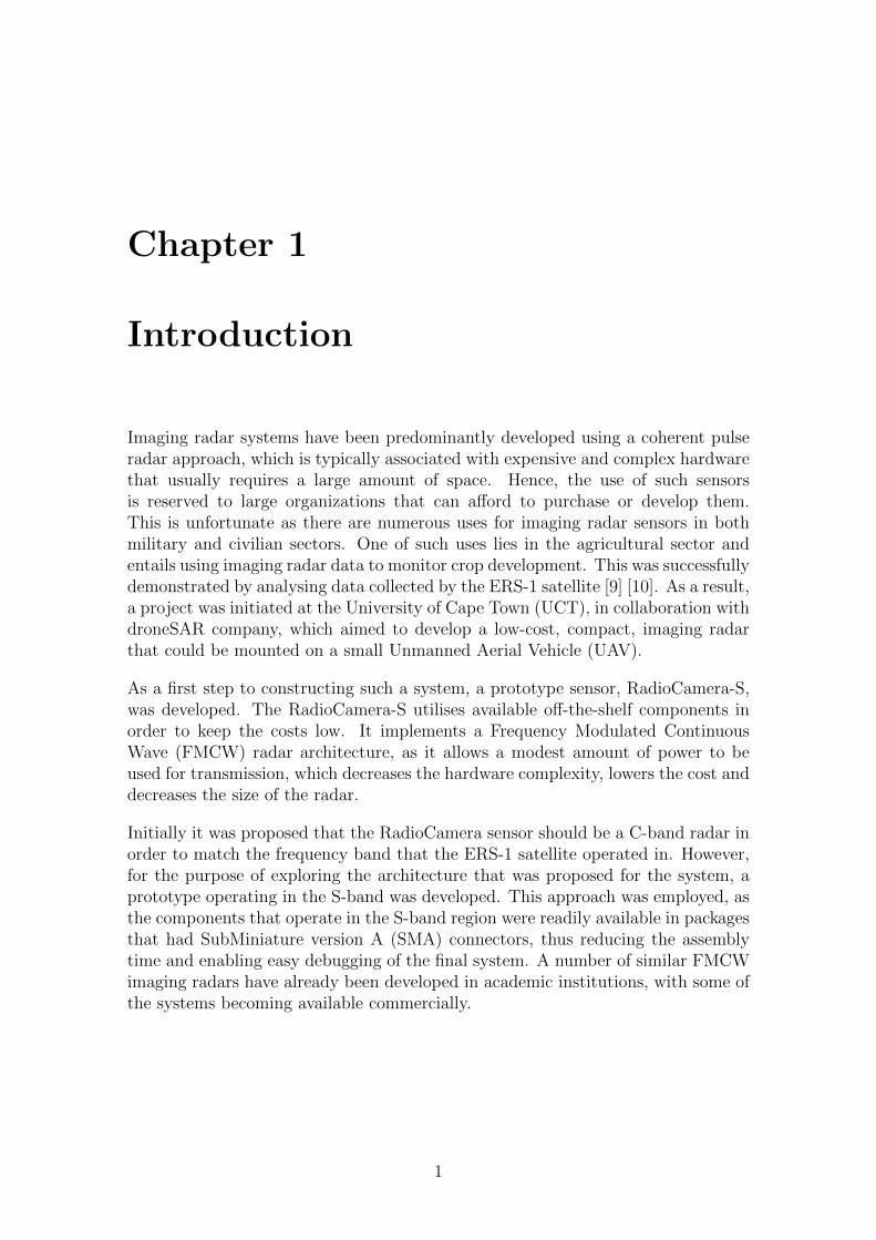
Furthermore, the system parameters had to be chosen in accordance with a prede-fined operational geometry, as shown in Figure 1.1. The altitude of a small-scaleairborne platform (h), was set to be 500 metres, with a propagation velocity of 30m/s. In this scenario the radar is set to point perpendicularly to the direction ofpropagation of the platform, which in the case of the figure provided is into thepage. The antenna beam is pointed towards the ground, with the requirement thata swath width (∆Y ) of a 1000 metres is illuminated and offset (Roffset) from nadirby 500 metres. The ground range resolution (δy) is required to be approximately 1metre mid-swath.
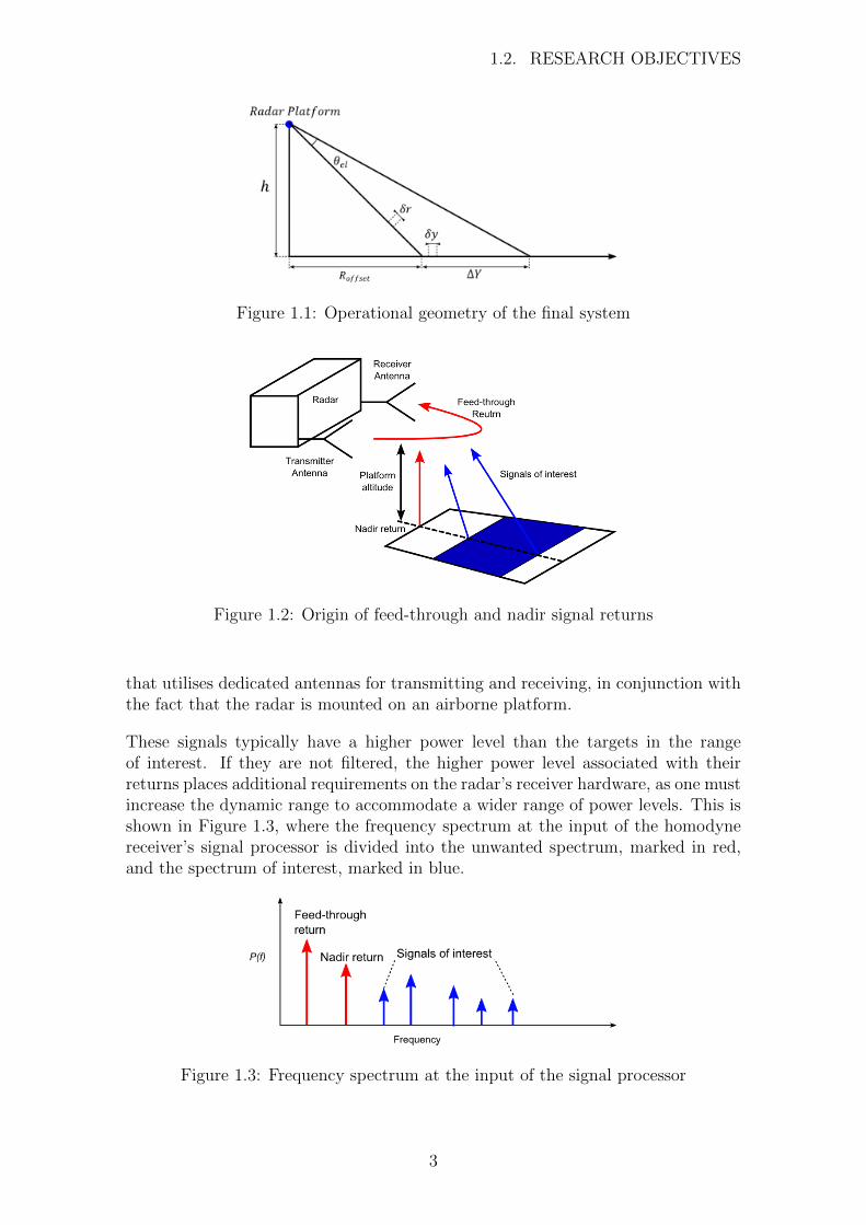
The second objective of this research project is to provide a solution for filteringthe feed-through and the nadir return signals. The two signals form a part of thereceived signal spectrum, which is produced when the received signal is mixed witha portion of the transmitted signal (See Appendix A). As Figure 1.2 shows, theseunwanted signals arise from the geometry associated with an imaging radar system
2
1.2. RESEARCH OBJECTIVES
Figure 1.1: Operational geometry of the final system
Figure 1.2: Origin of feed-through and nadir signal returns
that utilises dedicated antennas for transmitting and receiving, in conjunction withthe fact that the radar is mounted on an airborne platform.
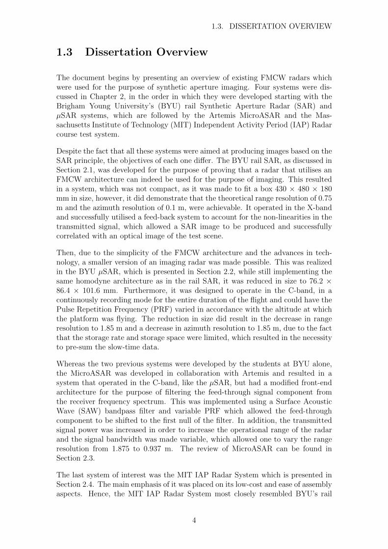
These signals typically have a higher power level than the targets in the rangeof interest. If they are not filtered, the higher power level associated with theirreturns places additional requirements on the radar’s receiver hardware, as one mustincrease the dynamic range to accommodate a wider range of power levels. This isshown in Figure 1.3, where the frequency spectrum at the input of the homodynereceiver’s signal processor is divided into the unwanted spectrum, marked in red,and the spectrum of interest, marked in blue.
Figure 1.3: Frequency spectrum at the input of the signal processor
3
1.3. DISSERTATION OVERVIEW
1.3 Dissertation Overview
The document begins by presenting an overview of existing FMCW radars whichwere used for the purpose of synthetic aperture imaging. Four systems were dis-cussed in Chapter 2, in the order in which they were developed starting with theBrigham Young University’s (BYU) rail Synthetic Aperture Radar (SAR) andµSAR systems, which are followed by the Artemis MicroASAR and the Mas-sachusetts Institute of Technology (MIT) Independent Activity Period (IAP) Radarcourse test system.
Despite the fact that all these systems were aimed at producing images based on theSAR principle, the objectives of each one differ. The BYU rail SAR, as discussed inSection 2.1, was developed for the purpose of proving that a radar that utilises anFMCW architecture can indeed be used for the purpose of imaging. This resultedin a system, which was not compact, as it was made to fit a box 430 × 480 × 180mm in size, however, it did demonstrate that the theoretical range resolution of 0.75m and the azimuth resolution of 0.1 m, were achievable. It operated in the X-bandand successfully utilised a feed-back system to account for the non-linearities in thetransmitted signal, which allowed a SAR image to be produced and successfullycorrelated with an optical image of the test scene.
Then, due to the simplicity of the FMCW architecture and the advances in tech-nology, a smaller version of an imaging radar was made possible. This was realizedin the BYU µSAR, which is presented in Section 2.2, while still implementing thesame homodyne architecture as in the rail SAR, it was reduced in size to 76.2 ×86.4 × 101.6 mm. Furthermore, it was designed to operate in the C-band, in acontinuously recording mode for the entire duration of the flight and could have thePulse Repetition Frequency (PRF) varied in accordance with the altitude at whichthe platform was flying. The reduction in size did result in the decrease in rangeresolution to 1.85 m and a decrease in azimuth resolution to 1.85 m, due to the factthat the storage rate and storage space were limited, which resulted in the necessityto pre-sum the slow-time data.
Whereas the two previous systems were developed by the students at BYU alone,the MicroASAR was developed in collaboration with Artemis and resulted in asystem that operated in the C-band, like the µSAR, but had a modified front-endarchitecture for the purpose of filtering the feed-through signal component fromthe receiver frequency spectrum. This was implemented using a Surface AcousticWave (SAW) bandpass filter and variable PRF which allowed the feed-throughcomponent to be shifted to the first null of the filter. In addition, the transmittedsignal power was increased in order to increase the operational range of the radarand the signal bandwidth was made variable, which allowed one to vary the rangeresolution from 1.875 to 0.937 m. The review of MicroASAR can be found inSection 2.3.
The last system of interest was the MIT IAP Radar System which is presented inSection 2.4. The main emphasis of it was placed on its low-cost and ease of assemblyaspects. Hence, the MIT IAP Radar System most closely resembled BYU’s rail
4
1.3. DISSERTATION OVERVIEW
SAR. It operated in the S-band and consisted of six coaxial microwave parts inthe front-end and two metallic cans for the transmitter and receiver antennas. Thereceiver utilised a homodyne architecture, similar to the rail SAR and the µSAR,with the output of the receiver digitised by a computer sound card, which placed alimit on the beat frequency signal spectrum, which in turn resulted in limiting therange of the radar to 272 m (in accordance with the operational parameters chosenfor the practical tests). This system provided a simple framework for a FMCWradar that could be used for Doppler and FMCW ranging, as well as for crude SARimaging.
Chapter 3 presents the design considerations that had to be accounted for in orderto satisfy the limitations of the user required hardware. Some of the more notableconstraints are imposed by the LMX2492EVM waveform generator, as it determinesthe bandwidth of the signal, as well as the minimum and maximum PRI rates, andthe Red Pitaya, which was used to digitise the data.
Then the geometry constraints are outlined in Section 3.2. The airborne geometryconstraints are explained, with reference to the signal bandwidth requirements, PRIand the antenna elevation beamwidth. Transmitted waveform parameters are thenproposed for the use in such an operating geometry. This is followed by a briefdescription of the ground based radar parameter requirements.
The two-channel filtering method is expanded on in Section 3.3, where two modes ofoperation are presented and explained graphically. A model is then derived for oneof the modes of operation. This is followed by a derivation of a system specificationfor a RadioCamera-S radar system.
Once the limitations and architecture overview is provided, a look at the hardwareimplementation is given in Chapter 4. The system was divided into three modules,namely: the transmitter, antenna and the receiver. Each module is examined in aseparate section.
The transmitter module is discussed from the point of its two main functionalities,which are to generate a waveform and amplify the modulated waveform to a desiredlevel. The antenna module presents the design procedure that was followed toimplement circular waveguide antenna designs, with the return loss and isolationplots demonstrated to verify the produced antennas.
The receiver module is described from the point of view of two channels. The mainchannel is analysed in more detail, as the input saturation power, the noise figure aswell as the receiver sensitivity parameters are derived. Then a brief overview of thehousing that is used to hold the three modules together is given. Chapter 5 focuseson the testing procedures, results and discussion of results for the RadioCamera-Sradar. First the transmitter module was tested by referring to the waveform gen-eration and the properties of the generated waveforms that allow one to determineif the synthesiser is indeed producing a correct waveform. Then the power level ofthe two transmitter and the two receiver channels were displayed.
After the two modules were tested separately the system tests were carried out.
5
1.3. DISSERTATION OVERVIEW
First, a delay-line testing procedure demonstrates the frequency components thatare produced when two waveforms with a PRI of 2 µs are offset from one anotherand how the Red Pitaya can be used to sample a particular region. Then the systemis completely assembled and tested in a known environment in order to be able tocorrelate the acquired data with the actual distances to targets.
After a number of tests that examine a single signal return are carried out, aRange-Time-Intensity plot is generated that demonstrates the movement of a singlereflector in the scene of interest.
Mode One filtering technique was used successfully to demonstrate the attenuationof the feed-through signal by utilising the properties of the video amplifiers gainresponse.
Chapter 6 is the last chapter of the dissertation, which draws conclusions by pro-viding a cross examination of the requirements that were set out at the start of theresearch project with the results that were obtained through theoretical analysisand testing. This is demonstrated in Section 6.1, Section 6.2 is focused on therecommendations for future work that can be carried out on the RadioCamera-Sprototype, as well as the future RadioCamera revisions.
There are two Appendices, Appendix A introduces the reader to the architecture ofa basic FMCW radar setup and gives a brief outline of the imaging radar operation.This is followed by Appendix B, which aims to provide an overview of the designconsiderations that one needs to account for when designing an FMCW radar.
6
Chapter 2
Overview of Existing FMCWImaging Radar Systems
During the last 14 years, the use of FMCW radar architecture for the purpose ofimaging has received close attention in academic circles. A number of researchprojects showed promising results and in some cases lead to the development ofcommercial imaging radar systems. This chapter aims to summarise the specifica-tions, design decisions and the performance of a number of those systems startingwith the Brigham Young University’s (BYU) rail Synthetic Aperture Radar (SAR)and µSAR, in Sections 2.1 and 2.2, respectively. The commercial system that wasthe successor to the first two BYU systems, the Artemis MicroASAR is discussedin Section 2.3, with the MIT IAP radar course test system examined last in Sec-tion 2.4. The chapter ends with a short summary in Section 2.5
2.1 BYU rail SAR
In 2002 a radar rail system was developed by Ryan L.Smith at the Brigham YoungUniversity, with the purpose of demonstrating that a radar that utilizes an FMCWarchitecture, can be used for the purpose of synthetic aperture imaging [1]. Thedimensions of the system were tailored to the size of YINSAR, which was a pulsedairborne SAR system developed at BYU and was made to fit a rack-mountable boxof 430×480×180 mm in size [12].
2.1.1 Specifications
The specifications of the radar are provided in Table 2.1. The operation frequencyrange is found in the X-band region and centred on 9.8 GHz, with a bandwidthof 200 MHz. The bandwidth of the transmitted signal as shown in [13] and [6]determines the range resolution of the radar, in accordance with Equation 2.1,
7

2.1. BYU RAIL SAR
δr =c
2∆f, (2.1)
where ∆f is the bandwidth and c is the speed of electromagnetic propagation infreespace. Hence, the maximum range resolution of this system is 0.75 m. As theplatform operates at 0 m elevation this corresponds with the effective ground rangeresolution and no further correction needs to be made.
Table 2.1: BYU rail SAR SpecificationsRadar Parameters
Frequency Band X-BandTx Centre Frequency 9.8 GHzTx Power 16 dBmChirp Period 1 ms (500 µs for bench tests)Minimum PRF 700 Hz (2.93 Hz for bench tests)Bandwidth 200 MHzDimensions 430×480×180 mmReceiver Noise Figure 4 dBChirp Generation VCOModulation Saw-tooth
Antenna ParametersAntenna Type Slotted Waveguide3-dB Beamwidth 10◦ azimuth × 45◦ elevationAntenna Gain 17 dBCenter Frequency 9.9 GHz
Operating SpecificationsRange Resolution 0.75 mTheoretical Azimuth Resolution 0.1 mPlatform Velocity 0.327 m/sNominal Platform Elevation 0 m
In order for the calculated range resolution to be achieved, one must ensure thatthe two-way propagation delay that is associated with an illuminated target at aparticular range is much smaller than the chirp period (PRI) of the radar. This isshown in [14] and can be expressed as:
tdelay =2× rc� PRI, (2.2)
where tdelay is the two-way propagation delay and r is the distance to target. There-fore, with the rail SAR PRI of 500 µs, the two-way propagation delay that will resultin a 80 percent overlap of the transmitted waveform with the received waveform is100 µs. This corresponds to a range of 15 km. However, the true range of the radar
8
2.1. BYU RAIL SAR
will also be limited by the power of the transmitted signal and additional param-eters that can be seen in the Radar Range Equation for a FMCW SAR system asderived in [5].
The velocity (v) of the rail SAR platform is 0.327 m/s, this parameter, in conjunc-tion with the wavelength (λ) of the transmitted signal and the antenna azimuthbeamwidth (θaz), determines the azimuth bandwidth (∆faz) of the system [1] ac-cording to:
∆faz =2vθazλ
. (2.3)
The azimuth bandwidth can then be used to determine the resolution of the radarin the azimuth direction (δx), according to Equation 2.4, which in this case is 0.1 m.This is partially determined by the 10 degree 3-dB bandwidth of the antennas, whichwere employed. Two antennas were employed, where one was transmitting and theother receiving. This configuration was realised in order to increase the isolationbetween the transmitter and receiver. The antennas were of slotted waveguide typewith a gain of 17 dB.
δx =v
∆faz=Daz
2(2.4)
Azimuth resolution of the radar is also used to determine the minimum value of thePulse Repetition Frequency (PRF), as the bandwidth needs to satisfy the Nyquistcriterion, hence the minimum PRF of the radar is [1]:
PRFmin = 2× 2vθazλ
. (2.5)
In the case where the above criterion is not accounted for and a lower PRF valueis utilised, the antenna mainlobe patterns as transmitted from different locationsalong the propagation trajectory of the radar, may overlap and cause Doppler am-biguity [15], this is explained in more detail in Appendix B.1.1.
2.1.2 Radar Design
The radar front-end of the rail SAR resembles a homodyne (direct conversion)architecture that mixes a replica of the transmitted signal with the received signaldirectly to baseband. A simplified block diagram can be seen in Figure 2.1(a),which shows that it has two receiver channels. The two channel design adds theability to carry out interferometry. A photo of the assembled system can be seenin Figure 2.1(b).
During the design phase, the radar system was divided into seven modules, whichare the Main Driver/Power Plane module, Radio Frequency (RF) Transmitter, Low
9

2.1. BYU RAIL SAR
(a) Simplified Block Diagram (b) Assembled System
Figure 2.1: BYU rail SAR System [1]
Noise Amplifier (LNA), RF mixer, Baseband module, Power Supply Unit (PSU) andDigitiser/Image Processor module. The FMCW Source, which is divided betweenthe Driver/Power Plane module and the RF Transmitter module, consists of aPIC16 microcontroller with a 14 bit Digital-to-analogue Converter (DAC), a lowpassfilter and a Voltage Controlled Oscillator (VCO).
The microcontroller together with the lowpass filter produces an analogue controlsignal for the VCO, which outputs a saw-tooth modulated waveform. In order toensure linearity of the output waveform, a feedback system is implemented thattunes the VCO control signal in order to account for the non-linearities of theVCO (more details on the feedback system can be found in Appendix B.1.2). Thelinearity of the waveform influences projected range resolution and range ambiguityof the radar, as was shown in [14] and explained in more detail in Appendix B.1.1.
The output of the VCO is fed into a ring coupler, which splits the signal into four,with two ports at 16 dBm and the other two at 26 dBm. One 16 dBm signal is sentdirectly to the transmitter antenna and the other one is left for testing purposes.The 26 dBm signals are fed to the LO port of the RF mixer.
The LNA module is designed to have a 50 dB Gain and 4 dB Noise Figure (NF). Thenoise figure of the LNA is required to be low as it is the main component that influ-ences the overall receiver NF. This is explained in more detail in Appendix B.3.1.The module consists of a four stage amplifier, where the first stage is designed forlow noise, stage two and three are designed for maximum gain and stage four isdesigned for maximum gain and maximum output power.
Once the received signal is amplified by the LNA, a HMC220S08 RF mixer isemployed for the purpose of de-chirping the received signal in the RF mixer module.The RF and LO ports operating frequency range is 5.9 to 10 GHz, with the outputfrequency range of DC to 3.5 GHz at the IF port. In order to ensure that theexpected performance, as outlined by the documentation, is achieved, the LO port
10

2.2. BYU µSAR
must be driven by a signal with a power level of 10 dBm.
The IF gain module consists of two amplifiers: a 26 dB gain LM7121 video opera-tional amplifier and a variable AD8321 amplifier that has variable gain in range of-28 to 26 dB. The gain of AD8321 amplifier was designed to be set by the PIC16microcontroller using an SPI interface. The bandwidth of the IF gain stage was 120MHz, this places a limitation on the beat frequency spectrum that can be analysedand thus on the range of the radar.
Prior to digitisation the output of the gain stage was passed through a lowpassfilter. The design of the system allowed the filter to be removed in order to enablethe operator to change the cut-off frequency of the spectrum of interest. This allowsone to account for the sampling rate of the digitiser without resulting in aliasing.
2.1.3 Performance
The performance analysis of the rail SAR system was initially carried out in theinverse SAR configuration, where a corner reflector was used as a target that wasmoving with a velocity of 0.327 m/s. The resultant range and azimuth resolutionthat was obtained corresponded to the theoretically calculated range resolution of0.75 m and azimuth resolution of 0.1 m.
Then a rail SAR test was carried out, where the sensor was moved along a rail atconstant velocity. The collected data was processed to form an image which showedconsistency with the optical image of the scene.
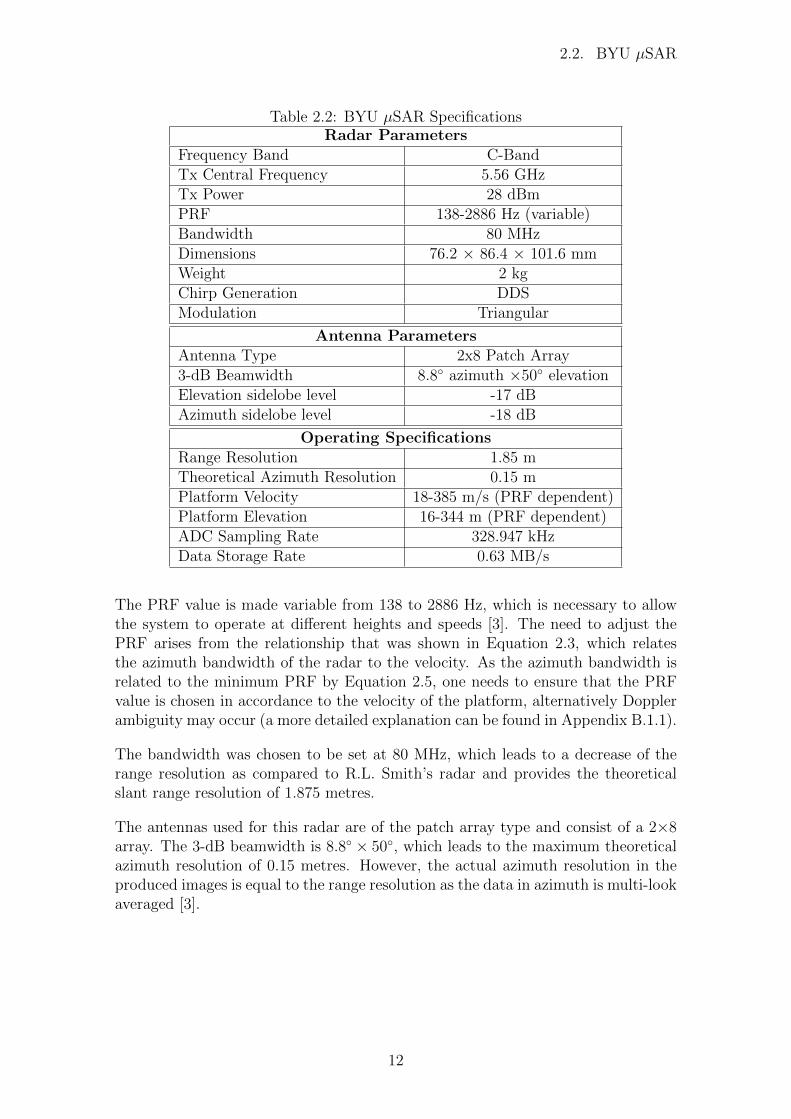
2.2 BYU µSAR
BYU µSAR system was developed in 2006 and essentially builds upon the previoussystem that was designed by R. L. Smith. The radar was designed to fit on a smalllow-altitude UAV with a wing span of six feet for the purpose of imaging the Arcticsea ice. The use of a FMCW architecture, allowed the costs to be kept low, relativeto the costs associated with more traditional pulsed imaging radars[3]. Subsequentsections will cover the specifications of the system, as well as the design aspects ofthe radar.
2.2.1 Specifications
Table 2.2, shows the specification of the radar system. The frequency band chosenfor this design was the C-Band and the center frequency of operation is 5.56 GHz,which falls into the unlicensed Wi-Fi band. The transmitted signal power is 28dBm, which is higher than the transmitter power of rail SAR (Section 2.1). Theincrease in transmitted power leads to the increase of the operational range, inaccordance with the Radar Range Equation [5].
11
2.2. BYU µSAR
Table 2.2: BYU µSAR SpecificationsRadar Parameters
Frequency Band C-BandTx Central Frequency 5.56 GHzTx Power 28 dBmPRF 138-2886 Hz (variable)Bandwidth 80 MHzDimensions 76.2 × 86.4 × 101.6 mmWeight 2 kgChirp Generation DDSModulation Triangular
Antenna ParametersAntenna Type 2x8 Patch Array3-dB Beamwidth 8.8◦ azimuth ×50◦ elevationElevation sidelobe level -17 dBAzimuth sidelobe level -18 dB
Operating SpecificationsRange Resolution 1.85 mTheoretical Azimuth Resolution 0.15 mPlatform Velocity 18-385 m/s (PRF dependent)Platform Elevation 16-344 m (PRF dependent)ADC Sampling Rate 328.947 kHzData Storage Rate 0.63 MB/s
The PRF value is made variable from 138 to 2886 Hz, which is necessary to allowthe system to operate at different heights and speeds [3]. The need to adjust thePRF arises from the relationship that was shown in Equation 2.3, which relatesthe azimuth bandwidth of the radar to the velocity. As the azimuth bandwidth isrelated to the minimum PRF by Equation 2.5, one needs to ensure that the PRFvalue is chosen in accordance to the velocity of the platform, alternatively Dopplerambiguity may occur (a more detailed explanation can be found in Appendix B.1.1).
The bandwidth was chosen to be set at 80 MHz, which leads to a decrease of therange resolution as compared to R.L. Smith’s radar and provides the theoreticalslant range resolution of 1.875 metres.
The antennas used for this radar are of the patch array type and consist of a 2×8array. The 3-dB beamwidth is 8.8◦ × 50◦, which leads to the maximum theoreticalazimuth resolution of 0.15 metres. However, the actual azimuth resolution in theproduced images is equal to the range resolution as the data in azimuth is multi-lookaveraged [3].
12
2.2. BYU µSAR
2.2.2 Radar Design
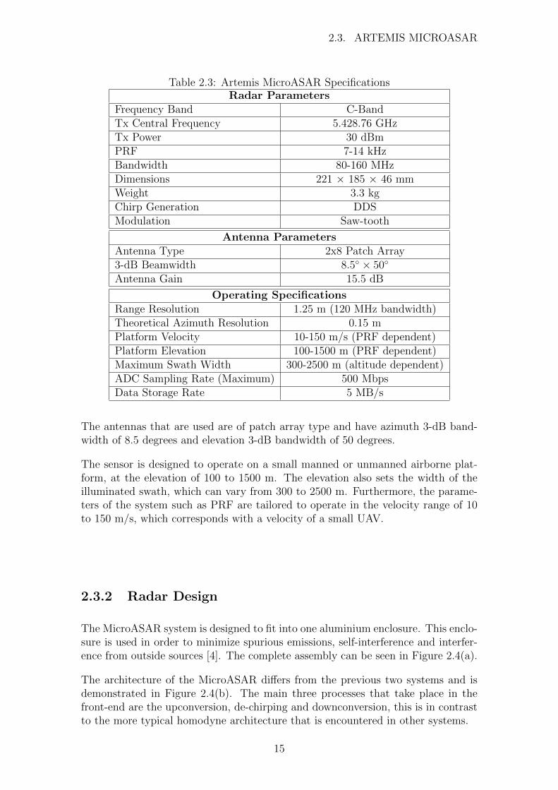
The system architecture is divided into five modules, which are the transmitter,receiver, power, digital and the Analogue-to digital converter (ADC).
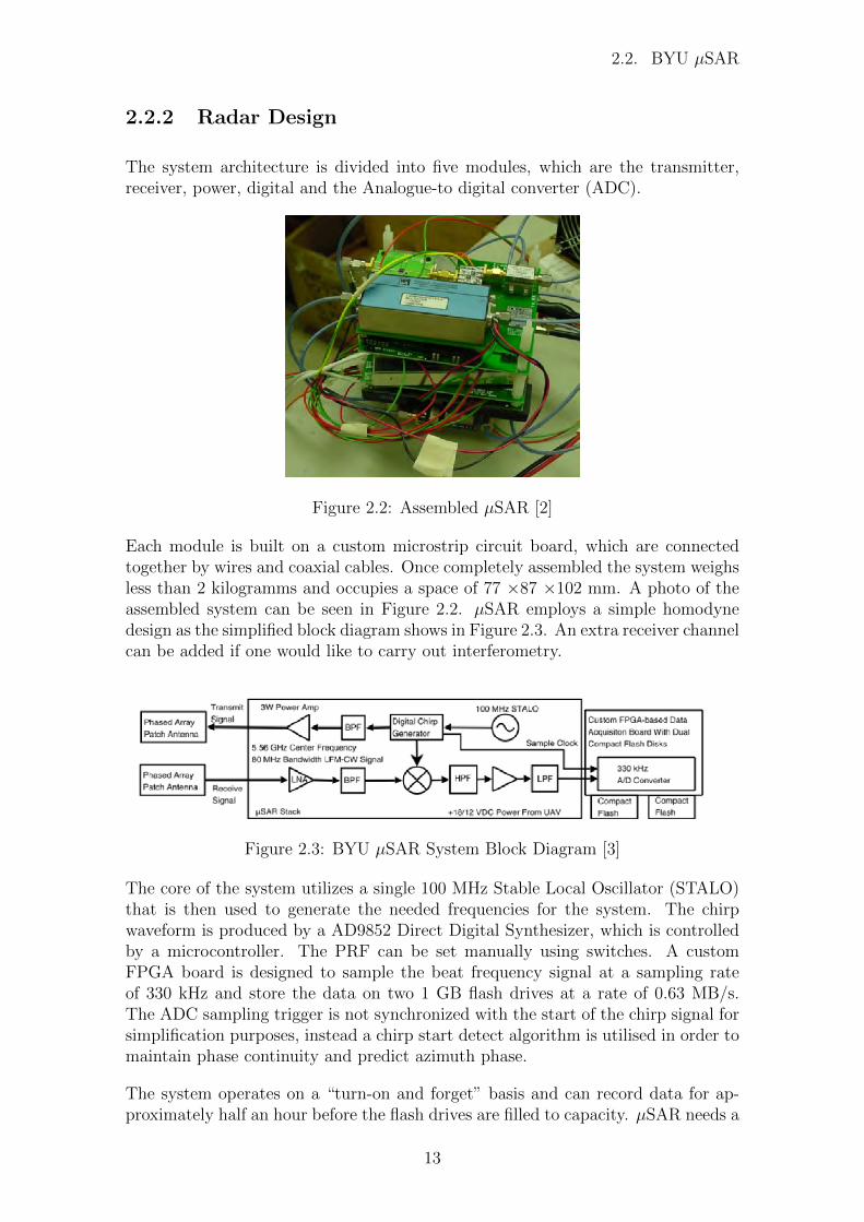
Figure 2.2: Assembled µSAR [2]
Each module is built on a custom microstrip circuit board, which are connectedtogether by wires and coaxial cables. Once completely assembled the system weighsless than 2 kilogramms and occupies a space of 77 ×87 ×102 mm. A photo of theassembled system can be seen in Figure 2.2. µSAR employs a simple homodynedesign as the simplified block diagram shows in Figure 2.3. An extra receiver channelcan be added if one would like to carry out interferometry.
Figure 2.3: BYU µSAR System Block Diagram [3]
The core of the system utilizes a single 100 MHz Stable Local Oscillator (STALO)that is then used to generate the needed frequencies for the system. The chirpwaveform is produced by a AD9852 Direct Digital Synthesizer, which is controlledby a microcontroller. The PRF can be set manually using switches. A customFPGA board is designed to sample the beat frequency signal at a sampling rateof 330 kHz and store the data on two 1 GB flash drives at a rate of 0.63 MB/s.The ADC sampling trigger is not synchronized with the start of the chirp signal forsimplification purposes, instead a chirp start detect algorithm is utilised in order tomaintain phase continuity and predict azimuth phase.
The system operates on a “turn-on and forget” basis and can record data for ap-proximately half an hour before the flash drives are filled to capacity. µSAR needs a
13

2.3. ARTEMIS MICROASAR
+12 V or +18 V input from the UAV and utilizes 18 W of power during operation.
2.2.3 Performance
The performance of the radar was tested during a test campaign, which includedinitial ground testing, where the system was mounted on a side of a car and drivenaround to record data, as well as further airborne tests, which entailed mountingthe radar on a Cessna 185 and flying over the Arctic Ocean. Another test flightwas carried out in Provo, Utah region to record images of rural landscapes.
The data which was presented in the available literature did not explicitly state theexact resolution that was achieved by the system. However, the testing campaignsdid show that an image of a scene could be reconstructed and the approximateposition of the corner reflectors that were set up in the test scene was determined.
The major aspect of the testing campaign for this system was related to evaluatingthe performance of the chirp start detection, auto-focusing and interference filteringalgorithms that are performed after the data was collected, as this dissertation isfocused on the development of the hardware for a FMCW radar, the analysis ofthose algorithms is omitted, but can be found in [2].
2.3 Artemis MicroASAR
Artemis MicroASAR is a successor to the BYU µSAR and was developed in collab-oration with Artemis in 2008 [4]. It is more flexible than the previous two systemsin that it can vary the signal bandwidth to achieve various range resolutions andcan carry out filtering of the feed-through signal by varying the PRF. This filteringtechnique is of particular interest as the second objective of this dissertation is tocarry out filtering of the feed-through and nadir return signals.
2.3.1 Specifications
The specifications of this system are summarised in Table 2.3. MicroASAR is alarger system than the µSAR and requires more power, this is a trade-off that needsto be made as transmission power level is increased to 30 dBm. The transmittedsignal is in the C-band region, centred at 5428.76 MHz. The bandwidth of thesystem can be varied between 80 to 160 MHz, which can provide a maximum rangeresolution of 0.93 m.
The PRF can be varied between the values of 7 to 14 kHz. This is utilized in orderto account for the change in velocity and altitude of the platform, as in the µSARcase. However, the change in PRF is also used to carry out feed-through signalfiltering, as will be shown in Section 2.3.3.
14
2.3. ARTEMIS MICROASAR
Table 2.3: Artemis MicroASAR SpecificationsRadar Parameters
Frequency Band C-BandTx Central Frequency 5.428.76 GHzTx Power 30 dBmPRF 7-14 kHzBandwidth 80-160 MHzDimensions 221 × 185 × 46 mmWeight 3.3 kgChirp Generation DDSModulation Saw-tooth
Antenna ParametersAntenna Type 2x8 Patch Array3-dB Beamwidth 8.5◦ × 50◦
Antenna Gain 15.5 dB
Operating SpecificationsRange Resolution 1.25 m (120 MHz bandwidth)Theoretical Azimuth Resolution 0.15 mPlatform Velocity 10-150 m/s (PRF dependent)Platform Elevation 100-1500 m (PRF dependent)Maximum Swath Width 300-2500 m (altitude dependent)ADC Sampling Rate (Maximum) 500 MbpsData Storage Rate 5 MB/s
The antennas that are used are of patch array type and have azimuth 3-dB band-width of 8.5 degrees and elevation 3-dB bandwidth of 50 degrees.
The sensor is designed to operate on a small manned or unmanned airborne plat-form, at the elevation of 100 to 1500 m. The elevation also sets the width of theilluminated swath, which can vary from 300 to 2500 m. Furthermore, the parame-ters of the system such as PRF are tailored to operate in the velocity range of 10to 150 m/s, which corresponds with a velocity of a small UAV.
2.3.2 Radar Design
The MicroASAR system is designed to fit into one aluminium enclosure. This enclo-sure is used in order to minimize spurious emissions, self-interference and interfer-ence from outside sources [4]. The complete assembly can be seen in Figure 2.4(a).
The architecture of the MicroASAR differs from the previous two systems and isdemonstrated in Figure 2.4(b). The main three processes that take place in thefront-end are the upconversion, de-chirping and downconversion, this is in contrastto the more typical homodyne architecture that is encountered in other systems.
15

2.3. ARTEMIS MICROASAR
(a) Complete assembly ofArtemis microASAR
(b) System block diagram
Figure 2.4: Artemis MicroASAR System [4]
The upconversion process is required as the DDS produces the saw-tooth modulatedwaveform at baseband and requires it to be stepped up to the carrier frequency,this technique is also used in µSAR. The de-chirping process is carried out in themixer, where a received signal is mixed with a frequency shifted version of thetransmitted signal. The transmitted signal is frequency shifted in order to place thebeat frequency spectrum in the bandpass filters pass band, with the feed-throughcomponents at the null of the bandpass filter, which is found at 1.1 MHz.
The output of the band pass filter is then downconverted to an offset video fre-quency where it is sampled by the ADC. In order to synchronise all the signalgeneration and the sampling at the ADC, a single Temperature Controlled CrystalOscillator (TCXO) is used.
A Virtex 4 FPGA is used to control the DDS and perform pre-storage processing,that entails pre-summing and filtering of data.
The hardware capabilities of the MicroASAR were extended by improving the max-imum sampling rate of the system to 500 Msps and increasing the data storage rateto 5 MB/s. The increase in sampling rate allows to extend the beat frequency band-width of the receiver, as ADC hardware must be able to sample at twice the highestfrequency present in the beat frequency signal. Hence, an improvement from thesampling rate of 328.947 ksps to 500 Msps, increases the theoretically possible beatfrequency band from 164.475 kHz to 250 MHz.
Further considerations have to be made as the width of the beat frequency spectrumwill be limited by the PRF and the storage rate. The storage rate places a limitationon the amount of data that can be recorded and thus, increasing the amount of datato improve the quality of the image can only be carried out until the maximumstorage rate is not fully utilised.
The multi-look averaging that is employed in µSAR and MicroASAR are the directresult of the fact that the system storage rate is not sufficient to process all the datathat is provided by the high PRF rate and requires a set number of consecutive chirpreturns in slow-time to be added up, averaged and stored as a single chirp return,
16
2.3. ARTEMIS MICROASAR
thereby degrading the azimuth resolution [4].
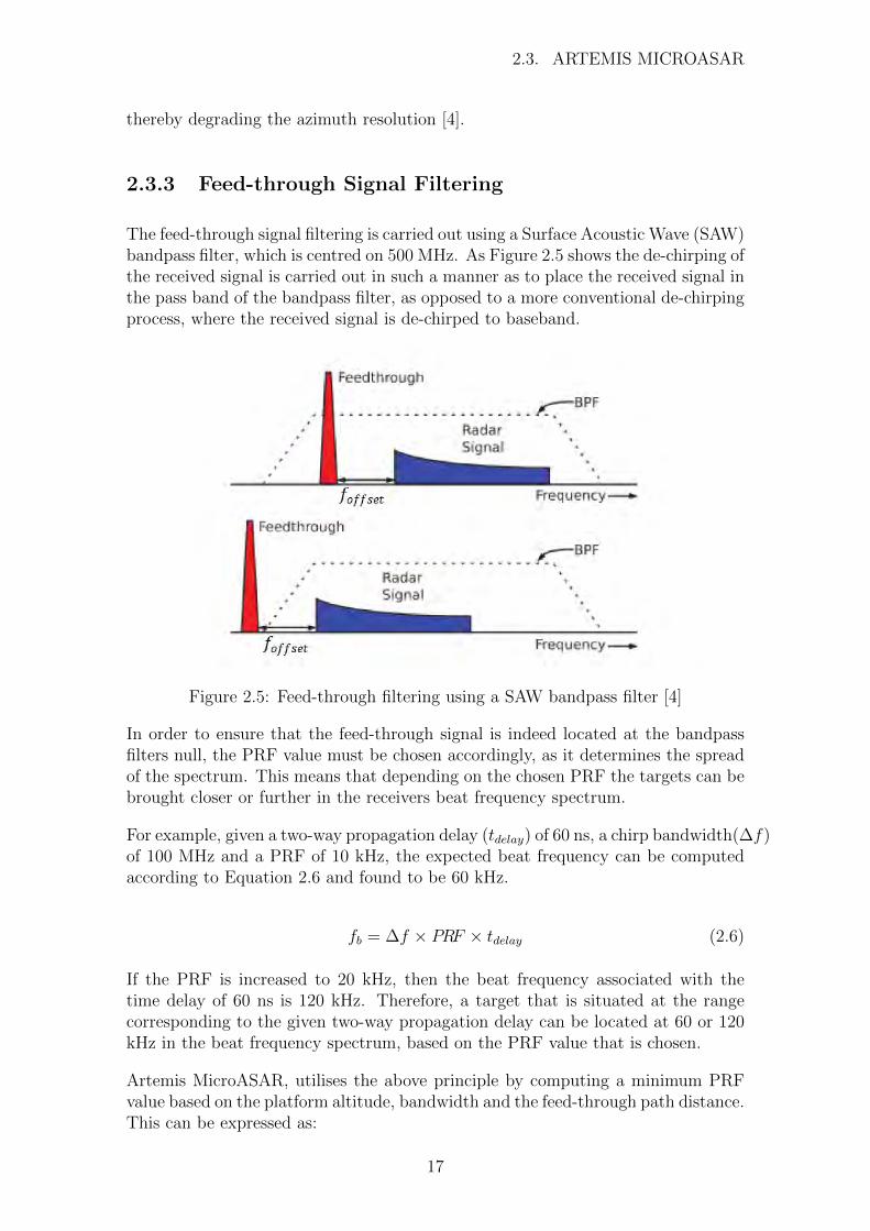
2.3.3 Feed-through Signal Filtering
The feed-through signal filtering is carried out using a Surface Acoustic Wave (SAW)bandpass filter, which is centred on 500 MHz. As Figure 2.5 shows the de-chirping ofthe received signal is carried out in such a manner as to place the received signal inthe pass band of the bandpass filter, as opposed to a more conventional de-chirpingprocess, where the received signal is de-chirped to baseband.
Figure 2.5: Feed-through filtering using a SAW bandpass filter [4]
In order to ensure that the feed-through signal is indeed located at the bandpassfilters null, the PRF value must be chosen accordingly, as it determines the spreadof the spectrum. This means that depending on the chosen PRF the targets can bebrought closer or further in the receivers beat frequency spectrum.
For example, given a two-way propagation delay (tdelay) of 60 ns, a chirp bandwidth(∆f)of 100 MHz and a PRF of 10 kHz, the expected beat frequency can be computedaccording to Equation 2.6 and found to be 60 kHz.
fb = ∆f × PRF × tdelay (2.6)
If the PRF is increased to 20 kHz, then the beat frequency associated with thetime delay of 60 ns is 120 kHz. Therefore, a target that is situated at the rangecorresponding to the given two-way propagation delay can be located at 60 or 120kHz in the beat frequency spectrum, based on the PRF value that is chosen.
Artemis MicroASAR, utilises the above principle by computing a minimum PRFvalue based on the platform altitude, bandwidth and the feed-through path distance.This can be expressed as:
17
2.3. ARTEMIS MICROASAR
PRFmin =cfoffset
2∆f(h− β), (2.7)
where foffset is the frequency that corresponds to the range difference between thefeed-through path and the nadir return, h is the platform height and β is the lengthof the effective free-space path that the feed-through signal takes [4].
Therefore, it can be seen that the minimum PRF value will vary, if the altitude ofthe platform is changing or the bandwidth of the signal is changed.
2.3.4 Performance
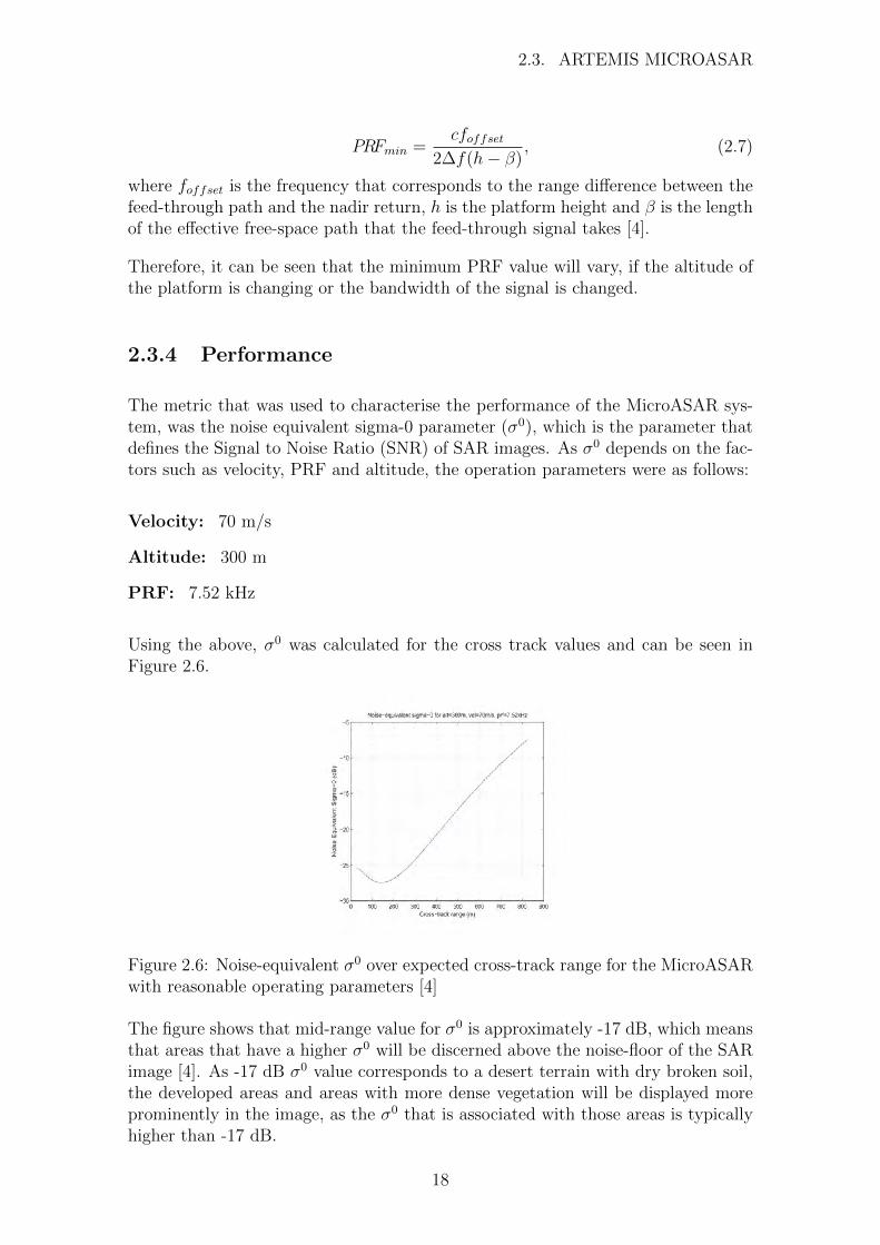
The metric that was used to characterise the performance of the MicroASAR sys-tem, was the noise equivalent sigma-0 parameter (σ0), which is the parameter thatdefines the Signal to Noise Ratio (SNR) of SAR images. As σ0 depends on the fac-tors such as velocity, PRF and altitude, the operation parameters were as follows:
Velocity: 70 m/s
Altitude: 300 m
PRF: 7.52 kHz
Using the above, σ0 was calculated for the cross track values and can be seen inFigure 2.6.
Figure 2.6: Noise-equivalent σ0 over expected cross-track range for the MicroASARwith reasonable operating parameters [4]
The figure shows that mid-range value for σ0 is approximately -17 dB, which meansthat areas that have a higher σ0 will be discerned above the noise-floor of the SARimage [4]. As -17 dB σ0 value corresponds to a desert terrain with dry broken soil,the developed areas and areas with more dense vegetation will be displayed moreprominently in the image, as the σ0 that is associated with those areas is typicallyhigher than -17 dB.
18
2.4. MIT IAP RADAR SYSTEM
2.4 MIT IAP Radar System
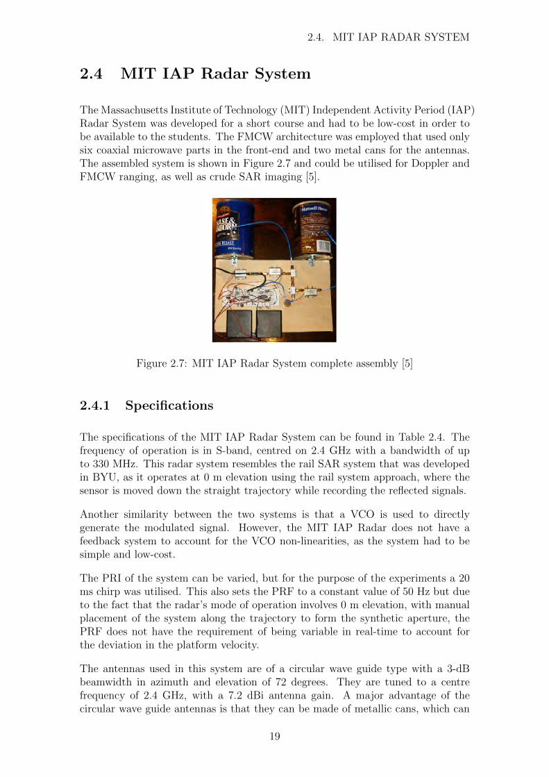
The Massachusetts Institute of Technology (MIT) Independent Activity Period (IAP)Radar System was developed for a short course and had to be low-cost in order tobe available to the students. The FMCW architecture was employed that used onlysix coaxial microwave parts in the front-end and two metal cans for the antennas.The assembled system is shown in Figure 2.7 and could be utilised for Doppler andFMCW ranging, as well as crude SAR imaging [5].
Figure 2.7: MIT IAP Radar System complete assembly [5]
2.4.1 Specifications
The specifications of the MIT IAP Radar System can be found in Table 2.4. Thefrequency of operation is in S-band, centred on 2.4 GHz with a bandwidth of upto 330 MHz. This radar system resembles the rail SAR system that was developedin BYU, as it operates at 0 m elevation using the rail system approach, where thesensor is moved down the straight trajectory while recording the reflected signals.
Another similarity between the two systems is that a VCO is used to directlygenerate the modulated signal. However, the MIT IAP Radar does not have afeedback system to account for the VCO non-linearities, as the system had to besimple and low-cost.
The PRI of the system can be varied, but for the purpose of the experiments a 20ms chirp was utilised. This also sets the PRF to a constant value of 50 Hz but dueto the fact that the radar’s mode of operation involves 0 m elevation, with manualplacement of the system along the trajectory to form the synthetic aperture, thePRF does not have the requirement of being variable in real-time to account forthe deviation in the platform velocity.
The antennas used in this system are of a circular wave guide type with a 3-dBbeamwidth in azimuth and elevation of 72 degrees. They are tuned to a centrefrequency of 2.4 GHz, with a 7.2 dBi antenna gain. A major advantage of thecircular wave guide antennas is that they can be made of metallic cans, which can
19
2.4. MIT IAP RADAR SYSTEM
be easily procured at a lower-cost than the other antenna types that were mentionedin this chapter.
The MIT IAP Radar System is low-cost and as a result does not aim to achievevery high performance in terms of ranging and image resolution.
Table 2.4: MIT IAP Radar System SpecificationsRadar Parameters
Frequency Band S-BandTx Central Frequency 2.4 GHzTx Power 13 dBmPRI 20 msBandwidth up to 330 MHzReceiver Noise Figure 1.2 dBChirp Generation VCOModulation Saw-tooth
Antenna ParametersAntenna Type Circular Waveguide3-dB Beamwidth 72◦
Antennae Coupling -39 dBAntenna Gain 7.2 dBiCenter Frequency 2.4 GHz
Operating SpecificationsEstimated Range Resolution 0.41 mTheoretical Azimuth Resolution 0.35 mPlatform elevation 0 mSampling rate 48 kHz
2.4.2 Radar Design
The system block diagram of the MIT IAP Radar System is provided in Figure 2.8,where a homodyne architecture can be seen.
The chirp waveform is generated by a VCO, which is driven by a XR-2206 rampgenerator. The signal is amplified by a ZX60-272LN-S+ amplifier, which is alsoused as the LNA in the receiver due to its low Noise Figure (NF) of 1.1 dB. Theoutput of the amplifier is connected to a ZX10-2-42+ two-way splitter, which feedsthe transmitter antenna and the LO port of the ZX-05-43MH+. This is a level 13mixer, hence the power of the signal at the the LO port is required to be 13 dBm.
The RF port of the mixer is connected to the output of the LNA, which amplifiesthe signal that is received by the receiver side antenna. The output of the mixer isa signal in the baseband region, which is filtered and amplified prior to digitisationby a computer sound card using the right audio channel of the 3.5 mm audio plug.
20

2.5. SUMMARY
Figure 2.8: MIT IAP Radar System Design [5]
In order to avoid phase errors the transmitted signal is synchronised with the re-ceived signal by recording a synchronisation pulse that the ramp generator producesat the start of every ramp. This is implemented using the left audio channel on a3.5 mm audio plug.
2.4.3 Performance
The performance of the MIT IAP Radar system is characterised by the expectedrange and imaging resolution. The range was calculated using the Radar RangeEquation [5], to yield a maximum range of 829 m for a target with a Radar CrossSection (RCS) of 10 m2 in the FMCW ranging mode and a maximum range of 2.2km in the SAR imaging mode for the same target.
The discrepancy between the two ranges can be explained by the fact that the SARprocessing adds an additional gain factor that corresponds to the number of profilesrecorded in azimuth to synthesise the aperture.
In either case, as the radar system has a limit on the highest beat frequency that itcan record, which is set to 15 kHz by the lowpass filter at the output of the videoamplifier. Given the PRI of 20 ms and a bandwidth of 330 MHz, the maximumrange that can be achieved is 272 m [5].
2.5 Summary
This chapter provided an overview of four distinct systems in the order in which theywere developed. All four systems utilised an FMCW architecture for the purpose ofimaging, however, each one had a different objective. The rail SAR system aimed atdemonstrating that the FMCW architecture can be used for the purpose of imaging,with the µSAR building on the developed framework and realising them in a smallerform factor. The MicroASAR, was a commercial system, that incorporated all thefeatures of the µSAR and implemented a method of feed-through signal removalby modifying the front-end architecture. Lastly, the MIT IAP Radar System wasexamined due to its emphasis on developing a low-cost FMCW radar that wascapable of SAR imaging.
21

Chapter 3
RadioCamera-S Design Criteria
The design procedure of the RadioCamera-S begins with the analysis of the con-straints that are related to the hardware requirements that were user defined. Thisis explained in Section 3.1. The effects of the operational geometry are discussed inSection 3.2, which is followed by the explanation of the two channel approach thatwas used to carry out the filtering of the feed-through and nadir return componentsin Section 3.3. Next, a ground based radar system specification that was developedas the result of the analyses performed in each section of this chapter is provided inSection 3.4, with a brief summary of the contents of the chapter in Section 3.5.
3.1 Hardware Considerations
The user requirements that were defined for this project included the followinghardware design considerations:
• S-Band operation
• Incorporate the LMX2492, 500 MHz to 14 GHz Low Noise Fractional Phase-locked Loop for ramp/chirp generation
• Implement a low-cost solution for antenna design
• Utilise the LMH6521 IF amplifier in the receiver
• Employ the Red Pitaya open source platform to acquire data
The reason for the above component selection is that: the LMX2492 ramp generator,LMH6521 IF amplifier and the Red Pitaya were relatively cheap, readily availableand came in a development board form factor with SMA connectors at all therequired ports. This simplified the testing procedure by reducing the time it tookto test different components and configurations, as well as enabled the author tomeet the project budget. Unfortunately, this component selection also placed someconstraints on the system, which are discussed next.
22

3.1. HARDWARE CONSIDERATIONS
3.1.1 Frequency of Operation and Waveform Generation
The waveform generator that was employed in the RadioCamera-S design was theLMX2492 evaluation module from Texas Instruments. The evaluation module com-prises of the LMX2492 Fractional Phase Locked Loop (PLL) with ramp generationcapabilities, a loop filter and a RFVC1843DS Voltage Controlled Oscillator.
The characteristics of the VCO essentially define the band of operation. It has threeoutputs which operate in three distinct bands: the S-band, C-band and X-band.Hence, it satisfies the S-band operation criterion, as it can produce a modulatedwaveform centred on 2.4125 GHz. An additional advantage is that it can also beintegrated into further RadioCamera prototypes, due to the fact that it offers aC-band output.
The evaluation module is restricted to a bandwidth of 175 MHz at the S-bandoutput and has a limit on the length of the PRI. The former is determined by theamplitude of the tuning voltage that the PLL can provide, whereas the latter isdetermined by a number of factors.
The maximum length of a single repetition of the waveform that can be achievedis determined by the LMX2492 method of programming the modulated waveform.It is capable of generating a configurable piecewise linear FM modulation profileof up to 8 segments [16], each segment can span a maximum of 1.31 ms in length.Hence, the absolute maximum PRI that is achievable is 10.48 ms. This is largelydetermined by the 100 MHz oscillator that is used to clock both PLL boards. Theoscillator defines the frequency of the phase detector in the PLL, which in turnrelates to the maximum length of each programmable segment.
Following that, the minimum PRI that can be achieved using the required hardwarewas determined experimentally to be 75 µs for a triangular ramp that ramps upand down over a 175 MHz bandwidth. If a faster sweep rate is attempted, a loss oflock occurs. The sweep rate of the system depends on the loop filter characteristics.Hence, should a faster ramp rate be desired a different loop filter configuration canbe utilised.
The type of modulation that can be produced using the given waveform generatorcan be varied. However, if a saw-tooth waveform with a direct return from the endto the start frequency is attempted, a loss of lock occurs due to the need to carryout a sweep of 175 MHz in almost no time. As a result a variation of a triangularwaveform is required.
3.1.2 Antenna Requirements
The low-cost requirement for the antenna resulted in the consideration of employingthe MIT IAP Radar System’s circular waveguide antenna design. Those antennasalready have defined parameters for the 3-dB elevation and azimuth beamwidth,which are 72 degrees. This leads to further constraints on the design if considered in
23

3.1. HARDWARE CONSIDERATIONS
conjunction with the velocity of the platform and the wavelength of the transmittedsignal, which define the azimuth bandwidth of the radar, according to Equation 2.3.
In order to avoid aliasing, the Nyquist criterion needs to be met, therefore theazimuth bandwidth needs to be sampled at twice the highest frequency. This placesa limit on the minimum PRF value, which can be calculated by using Equation 2.5.
Given the velocity of the platform to be 30 m/s, as pre-defined by the requirementfor the airborne geometry, the wavelength of 0.124 m, which corresponds to thecentre frequency of 2.4125 GHz, and the azimuth 3-dB beamwidth to be 72 degrees,the minimum PRF value is 1.216 kHz.
3.1.3 Video Amplifier
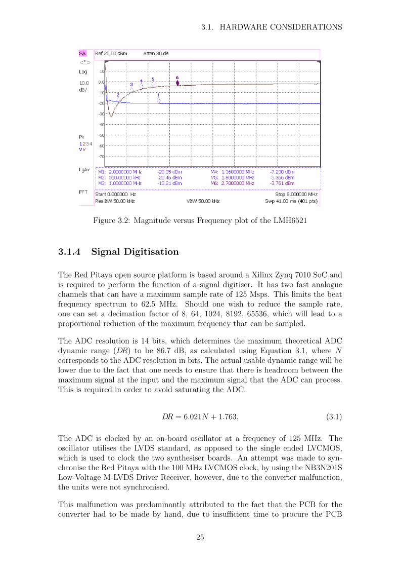
The LMH6521 IF amplifier was the video amplifier which was selected for theRadioCamera-S receiver chain. It is a Dual Digitally Controlled Variable GainAmplifier (DVGA), which is limited to a 26 dB maximum voltage gain. It has a3 dB Bandwidth of 1200 MHz. However, upon inspection of the Gain versus Fre-quency plot in the datasheet [17], which can be seen in Figure 3.1, it was foundthat signals in the frequency range from DC to approximately 1 MHz, are atten-uated and the actual gain of the amplifier only reaches the expected value fromapproximately 10 MHz.
Figure 3.1: Gain versus Frequency plot of the LMH6521
This was also determined experimentally with the results presented in Figure 3.2,where the blue trace is the -20 dBm input and the black trace is the amplifieroutput. It can be seen that below 500 kHz, the input signal from a signal generatoris attenuated by 10 dB, despite the fact that the gain setting of the amplifier is setto 20 dB. This places a limitation on the band of frequencies that can be used inthe baseband section of the receiver, as actual target returns that are below the -20dBm level tend to be filtered in the DC-500 kHz region.
24
3.1. HARDWARE CONSIDERATIONS
Figure 3.2: Magnitude versus Frequency plot of the LMH6521
3.1.4 Signal Digitisation
The Red Pitaya open source platform is based around a Xilinx Zynq 7010 SoC andis required to perform the function of a signal digitiser. It has two fast analoguechannels that can have a maximum sample rate of 125 Msps. This limits the beatfrequency spectrum to 62.5 MHz. Should one wish to reduce the sample rate,one can set a decimation factor of 8, 64, 1024, 8192, 65536, which will lead to aproportional reduction of the maximum frequency that can be sampled.
The ADC resolution is 14 bits, which determines the maximum theoretical ADCdynamic range (DR) to be 86.7 dB, as calculated using Equation 3.1, where Ncorresponds to the ADC resolution in bits. The actual usable dynamic range will belower due to the fact that one needs to ensure that there is headroom between themaximum signal at the input and the maximum signal that the ADC can process.This is required in order to avoid saturating the ADC.
DR = 6.021N + 1.763, (3.1)
The ADC is clocked by an on-board oscillator at a frequency of 125 MHz. Theoscillator utilises the LVDS standard, as opposed to the single ended LVCMOS,which is used to clock the two synthesiser boards. An attempt was made to syn-chronise the Red Pitaya with the 100 MHz LVCMOS clock, by using the NB3N201SLow-Voltage M-LVDS Driver Receiver, however, due to the converter malfunction,the units were not synchronised.
This malfunction was predominantly attributed to the fact that the PCB for theconverter had to be made by hand, due to insufficient time to procure the PCB
25
3.2. SYSTEM GEOMETRY CONSIDERATIONS
from the manufacturer. As a result the track width and spacing that is required bythe LVDS standard were not achieved, which resulted in signal degradation to thepoint where the ADC could not be clocked effectively.
The system could still operate asynchronously when a single shot FMCW rangingradar setup is employed. However, problems will arise if the system will operate inan imaging mode due to pulse to pulse phase errors.
The available data acquisition routines limit the number of samples that can berecorded continuously to 16384 samples. This places limitations on the time framethat can be sampled, as if 16384 samples are sampled at 125 Msps, then a maximumof 131 µs can be recorded. If the sample rate is decimated by a factor of 8, to 15.6Msps, this can be extended to a time period of 1.05 ms at the expense of thebandwidth. This time period will essentially be referred to as the maximum PRI,as the Red Pitaya is currently unable to digitise a longer PRI.
Lastly, as the Red Pitaya is a new system, which does not have a large user commu-nity supporting it, the application development time is extended, due to the lack ofdocumentation and previous user expertise. The above limitation of the number ofsamples that can be acquired at any one time is a fitting example, as it will requiretime and resources to modify the existing routines.
3.2 System Geometry Considerations
As was mentioned in Chapter 1, the RadioCamera project is aimed at designing aradar that will be compact enough to fit on a small UAV and operate in the C-band.The RadioCamera-S prototype on the other hand is a ground based system, thatis utilised to test the hardware and the architecture for the future revision thatwill be implemented in a small form factor. As a result there will be differencesin the expected operational range, waveform design criteria and the beat frequencyspectra of the airborne and ground based systems. This section aims to addressboth of the operational geometries and provide a framework for understanding theparameter variations due to the difference in operational conditions.
3.2.1 Airborne System Geometry Considerations
The geometry of the airborne system that was utilised to define the radar parameterscan be seen in Figure 3.3. The elevation of a small-scale airborne platform (h), wasset to be 500 metres. In this scenario the radar is set to point perpendicularly to thedirection of propagation of the platform, which in the case of the provided figureis into the page and has a velocity equal to 30 m/s. The antenna beam is pointedtowards the ground, with the requirement that a swath width (∆Y ) of a 1000 metresneeds to be illuminated and offset (Roffset) from nadir by 500 metres. The groundrange resolution (δy) is required to be approximately 1 metre mid-swath.
26

3.2. SYSTEM GEOMETRY CONSIDERATIONS
Figure 3.3: Operational geometry of the final system
The termsRs near andRs far correspond to the distance from the radar to the nearestpoint in the swath and to the furthest point in the swath in meters, respectively.Given the geometrical dimensions of the system, the range can be computed usingthe following equation:
Rs =√h2 +R2
ground, (3.2)
where h is the height (elevation) of the platform and Rground is the distance from thenadir to the point of intersection of the slant range with the ground plane. Usingthis equation the two ranges can be computed:
Rs near =√
5002 + 5002 = 707.1 (3.3)
Rs far =√
5002 + 15002 = 1581.1 (3.4)
Hence, the range profile that will be seen at the receiver can be illustrated byFigure 3.4, where the length (β) of the effective free space path that the feed-through signal takes is approximately 2 m (in accordance with [4]) and the radarelevation (h) is equal to 500 m.
The range values in the range profile are related to the frequency components of thebeat frequency spectrum through the two-way propagation delay that they produce.The associated time delays can be computed by using Equation 2.2. The resultsare presented in Table 3.1.
Once the two-way propagation delay for the targets of interest was computed itcan be related to the frequency components of the beat frequency spectrum by thefollowing relationship [18]:
27

3.2. SYSTEM GEOMETRY CONSIDERATIONS
Figure 3.4: RadioCamera-S typical range profile
Table 3.1: Relationship between range and two-way propagation delay of the returnsof interest
Return Range Time Delaym µs
Feed-through 2 0.0013Nadir return 500 3.333Near Swath 707.1 4.714Far Swath 1581.1 10.541
fbeat =∆f
∆ttdelay, (3.5)
where ∆f is the bandwidth of the signal and ∆t is the duration of the ramp (PRI).As the two-way propagation delay is constant for the target at the given range, thebeat frequency signal can be varied by changing the values of the bandwidth of thetransmitted signal and the ramp duration (PRI) of the waveform. However, thoseparameters are also responsible for additional factors that affect the performanceof the radar:
• Bandwidth of the signal needs to be high enough to satisfy the range resolutioncondition
• Two-way propagation delay of the furthest target must be much smaller thanthe PRI [14]
Furthermore, the geometry of the system also places a minimum requirement on theelevation beamwidth of the antenna. The above mentioned design considerationswill now be explained in more detail.
28

3.2. SYSTEM GEOMETRY CONSIDERATIONS
Signal Bandwidth
As the resolution requirements of the system dictate that the range resolution shouldbe approximately 1 m mid-swath, the slant resolution can be computed by usingthe following expression [1]:
δr =δy√
1 + h2
R2ground
, (3.6)
where δr is the slant range, δy is the ground range, h is the elevation of the platformand Rground is the ground range distance from nadir to the point of intersection ofthe slant range line of sight with the ground plane.
Given the geometry, the mid-swath point is located 1000 m away from nadir, takinginto account the 1 m ground resolution, the slant resolution is equal to 0.89 m.Hence, the minimum bandwidth (∆fmin) of the transmitted signal that can be usedto satisfy this slant range resolution can be computed by the following equation:
∆fmin =c
2δr, (3.7)
which results in ∆fmin equal to 168.5 MHz. As the maximum bandwidth of thetransmitter is 175 MHz, this criterion is satisfied.
Two-way Propagation Delay and PRI
According to [14], the two-way propagation delay of the furthest target needs to bemuch smaller than the PRI of the chirp signal. The exact ratio between the two isnot specified in literature, hence for the purpose of this dissertation, an assumptionwill be made that the two-way propagation delay must not be longer than 20% ofthe PRI.
Due to the fact that the furthest target that is to be illuminated by the radar islocated at 1581.1 m, with the corresponding two-way propagation delay of 10.541µs. The minimum PRI that can be employed by the system is computed by usingthe following equation:
PRImin =max(tdelay)× 100%
20%, (3.8)
and is equal to 52.66 µs. However, this is below the minimum PRI that theLMX2492EVM can generate, as it limits the PRI value at 75 µs. Hence, the minimusystem PRI is 75 µ. Furthermore, as the PRI and PRF are related according to theexpression:
PRF =1
PRI, (3.9)
29
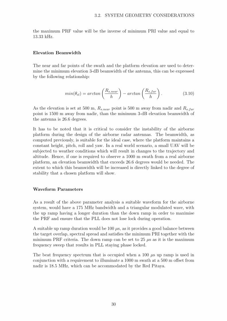
3.2. SYSTEM GEOMETRY CONSIDERATIONS
the maximum PRF value will be the inverse of minimum PRI value and equal to13.33 kHz.
Elevation Beamwidth
The near and far points of the swath and the platform elevation are used to deter-mine the minimum elevation 3-dB beamwidth of the antenna, this can be expressedby the following relationship:
min(θel) = arctan
(Rs near
h
)− arctan
(Rs far
h
). (3.10)
As the elevation is set at 500 m, Rs near point is 500 m away from nadir and Rs far
point is 1500 m away from nadir, than the minimum 3-dB elevation beamwidth ofthe antenna is 26.6 degrees.
It has to be noted that it is critical to consider the instability of the airborneplatform during the design of the airborne radar antennas. The beamwidth, ascomputed previously, is suitable for the ideal case, where the platform maintains aconstant height, pitch, roll and yaw. In a real world scenario, a small UAV will besubjected to weather conditions which will result in changes to the trajectory andaltitude. Hence, if one is required to observe a 1000 m swath from a real airborneplatform, an elevation beamwidth that exceeds 26.6 degrees would be needed. Theextent to which this beamwidth will be increased is directly linked to the degree ofstability that a chosen platform will show.
Waveform Parameters
As a result of the above parameter analysis a suitable waveform for the airbornesystem, would have a 175 MHz bandwidth and a triangular modulated wave, withthe up ramp having a longer duration than the down ramp in order to maximisethe PRF and ensure that the PLL does not lose lock during operation.
A suitable up ramp duration would be 100 µs, as it provides a good balance betweenthe target overlap, spectral spread and satisfies the minimum PRI together with theminimum PRF criteria. The down ramp can be set to 25 µs as it is the maximumfrequency sweep that results in PLL staying phase locked.
The beat frequency spectrum that is occupied when a 100 µs up ramp is used inconjunction with a requirement to illuminate a 1000 m swath at a 500 m offset fromnadir is 18.5 MHz, which can be accommodated by the Red Pitaya.
30
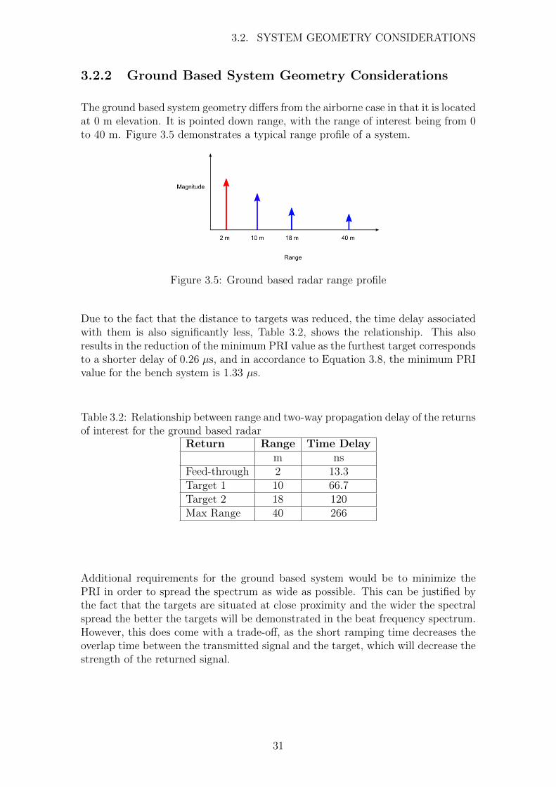
3.2. SYSTEM GEOMETRY CONSIDERATIONS
3.2.2 Ground Based System Geometry Considerations
The ground based system geometry differs from the airborne case in that it is locatedat 0 m elevation. It is pointed down range, with the range of interest being from 0to 40 m. Figure 3.5 demonstrates a typical range profile of a system.
Figure 3.5: Ground based radar range profile
Due to the fact that the distance to targets was reduced, the time delay associatedwith them is also significantly less, Table 3.2, shows the relationship. This alsoresults in the reduction of the minimum PRI value as the furthest target correspondsto a shorter delay of 0.26 µs, and in accordance to Equation 3.8, the minimum PRIvalue for the bench system is 1.33 µs.
Table 3.2: Relationship between range and two-way propagation delay of the returnsof interest for the ground based radar
Return Range Time Delaym ns
Feed-through 2 13.3Target 1 10 66.7Target 2 18 120Max Range 40 266
Additional requirements for the ground based system would be to minimize thePRI in order to spread the spectrum as wide as possible. This can be justified bythe fact that the targets are situated at close proximity and the wider the spectralspread the better the targets will be demonstrated in the beat frequency spectrum.However, this does come with a trade-off, as the short ramping time decreases theoverlap time between the transmitted signal and the target, which will decrease thestrength of the returned signal.
31

3.3. THE TWO-CHANNEL FILTERING APPROACH
3.3 The Two-Channel Filtering Approach
The proposed two channel filtering architecture is illustrated in Figure 3.6. Thewaveform generators S1 and S2 produce identical L-FMCW waveforms but have atime offset (toffset) between them. The “S1” with its respective signal St1 and “S2”,which produces the signal St2, is the notation that is employed in this dissertationto refer to the respective waveform generators when discussing the precedence ofwaveforms in the radar transmitter.
Figure 3.6: Simplified signal block diagram that demonstrates the main signal pathsassociated with the two channel filtering approach
The offset time can be related to a shift in frequency in the beat frequency spectrumat the output of the mixers. Based on the precedence of waveforms, two modes ofoperation can be identified:
Mode One - Signal St1 from waveform generator S1 is lagging signal St2
Mode Two - Signal St1 from waveform generator S1 is leading signal St2
Once the spectrum is shifted a high pass filter can be used to filter the unwantedsignals in the case of Mode One and a low pass filter can be used to filter theunwanted signals in Mode Two. The exact description of the two modes and howthey can be used to aid the filtering of the unwanted echoes is demonstrated usinga graphical approach and then followed by a mathematical model derivation.
3.3.1 Graphical Description
Figure 3.7 illustrates the two modes of operation as they were described above.
Mode One
In the main receiver channel the signal that contains the target information is mixedtogether in MXR2 with a copy of the signal produced in waveform generator S2,
32

3.3. THE TWO-CHANNEL FILTERING APPROACH
Figure 3.7: Two modes of operation of RadioCamera-S radar system
hence the time delay to target increases from the the value of tdelay to a value oftdelay + toffset. Hence, the frequency components that usually associate with thetdelay, will be translated in the frequency spectrum by a factor that is proportionalto toffset in the frequency domain. The conversion from the time to frequencydomain can be carried out using Equation 2.6 or 3.5. This process is illustrated inFigure 3.8.
Figure 3.8: Graphical representation of Mode One
Meanwhile, in the reference channel of the receiver, the two waveforms that were
33
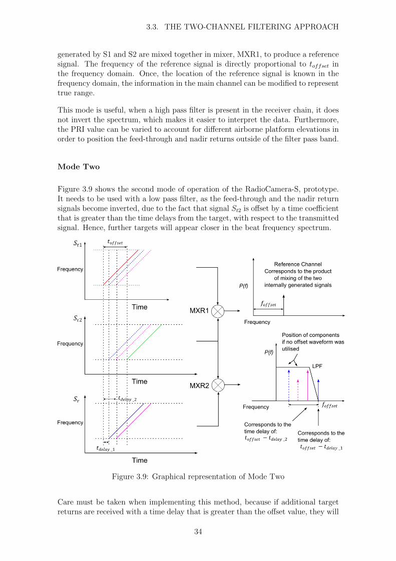
3.3. THE TWO-CHANNEL FILTERING APPROACH
generated by S1 and S2 are mixed together in mixer, MXR1, to produce a referencesignal. The frequency of the reference signal is directly proportional to toffset inthe frequency domain. Once, the location of the reference signal is known in thefrequency domain, the information in the main channel can be modified to representtrue range.
This mode is useful, when a high pass filter is present in the receiver chain, it doesnot invert the spectrum, which makes it easier to interpret the data. Furthermore,the PRI value can be varied to account for different airborne platform elevations inorder to position the feed-through and nadir returns outside of the filter pass band.
Mode Two
Figure 3.9 shows the second mode of operation of the RadioCamera-S, prototype.It needs to be used with a low pass filter, as the feed-through and the nadir returnsignals become inverted, due to the fact that signal St2 is offset by a time coefficientthat is greater than the time delays from the target, with respect to the transmittedsignal. Hence, further targets will appear closer in the beat frequency spectrum.
Figure 3.9: Graphical representation of Mode Two
Care must be taken when implementing this method, because if additional targetreturns are received with a time delay that is greater than the offset value, they will
34

3.3. THE TWO-CHANNEL FILTERING APPROACH
fold over the targets that are located at a time delay, which is less than the offsetvalue by the same margin.
3.3.2 Model Derivation
The method of filtering the signals which are located at a known range can alsobe expressed mathematically. This will be demonstrated by deriving the modelfor Mode One. If the waveform that is produced by waveform generator S1 isrepresented as:
St1 = ej(2πfct+µt2
2), (3.11)
where fc is the carrier frequency, t is the variation in time and µ is the chirprate (∆f
∆t). Then the waveform that is generated by waveform generator S2 and
triggered at a time offset of toffset from St1 can be expressed as:
St2 = ej(2πfc(t+toffset)+µ(t+toffset)
2
2). (3.12)
The amplitude coefficients of the waveforms are left out of this analysis for thepurpose of simplification. Those two waveforms are mixed together to producea reference channel of the receiver. The mixing process can be modelled as themultiplication of signal St1 by the complex conjugate of the time offset signal St2,the result of the mixing process is shown in Equation 3.13.
Sref = ej(−2πfctoffset−µ×t×toffset−µt2offset
2). (3.13)
The derivative of the phase corresponds to the frequency value of the signal, hence,the derivative of the Sref signal will yield the following:
fSref = −µtoffset. (3.14)
This can be used at a later stage to derive the range to target, once the beatfrequency of the target signal from the main receiver channel is known.
The signal at the receiver can be expressed as:
Srx = ej(2πfc(t−tdelay)+µ(t−tdelay)
2
2). (3.15)
where tdelay is the two-way propagation delay that corresponds to range to target.Srx signal contains the information from one target, if multiple targets were present,one would require to add all the exponential terms that correspond to each target.
35
3.4. SYSTEM SPECIFICATION
The signal at the main receiver channel is a result of mixing operation of signalsSt2 and signal Srx. Only the phase information of the output signal is presented inEquation 3.16 for ease of presentation:
φ(t) = 2πfc(tdelay − toffset) + µt(tdelay − toffset)−µ
2(t2delay − µtoffset) (3.16)
In order to determine what the resultant beat frequency component is, a derivativewith respect to time of the phase can be found:
fSmain = µ(tdelay + toffset). (3.17)
Equation 3.17 shows that the relationship between toffset and tdelay determines thebeat frequency of the target in the beat frequency spectrum of the main receiverchannel.
In order to obtain the true beat frequency value that corresponds to the actualrange to target the beat frequency components need to be added, this is shown inEquation 3.18.
fbeat = fSmain + fSref , (3.18)
if the values for the two beat frequencies are substituted from Equations 3.17and 3.14, Equation 3.18 becomes:
fbeat = µ(tdelay + toffset)− µtoffset = µtdelay. (3.19)
This essentially allows one to derive the true two-way propagation delay that cor-responds to the target position using a reference and a main receiver channel, whilefiltering the unwanted signals out. Mode Two operates on the similar premise,however, the signs change in the above equation as the spectrum is inverted due tothe fact that signal St2 is offset by a factor of −toffset from the target return andby the factor of −tdelay − toffset from the transmitted signal.
3.4 System Specification
After the analysis of the hardware limitations, as well as the predefined geometry, asystem specification can be proposed for the RadioCamera-S prototype that will berefined after the practical testing is carried out. Table 3.3 demonstrates the radar,antenna and operational parameters for the ground based system.
36
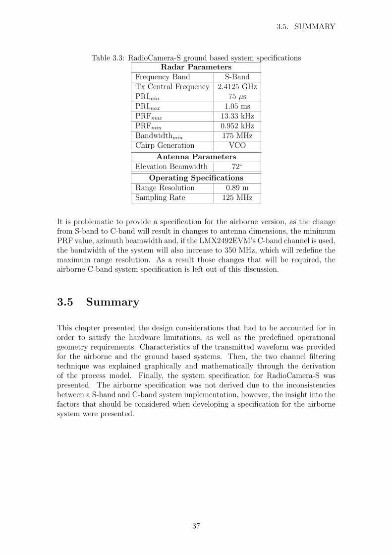
3.5. SUMMARY
Table 3.3: RadioCamera-S ground based system specificationsRadar Parameters
Frequency Band S-BandTx Central Frequency 2.4125 GHzPRImin 75 µsPRImax 1.05 msPRFmax 13.33 kHzPRFmin 0.952 kHzBandwidthmin 175 MHzChirp Generation VCO
Antenna ParametersElevation Beamwidth 72◦
Operating SpecificationsRange Resolution 0.89 mSampling Rate 125 MHz
It is problematic to provide a specification for the airborne version, as the changefrom S-band to C-band will result in changes to antenna dimensions, the minimumPRF value, azimuth beamwidth and, if the LMX2492EVM’s C-band channel is used,the bandwidth of the system will also increase to 350 MHz, which will redefine themaximum range resolution. As a result those changes that will be required, theairborne C-band system specification is left out of this discussion.
3.5 Summary
This chapter presented the design considerations that had to be accounted for inorder to satisfy the hardware limitations, as well as the predefined operationalgeometry requirements. Characteristics of the transmitted waveform was providedfor the airborne and the ground based systems. Then, the two channel filteringtechnique was explained graphically and mathematically through the derivationof the process model. Finally, the system specification for RadioCamera-S waspresented. The airborne specification was not derived due to the inconsistenciesbetween a S-band and C-band system implementation, however, the insight into thefactors that should be considered when developing a specification for the airbornesystem were presented.
37
Chapter 4
Hardware Implementation
The specification that was developed in Section 3.4 predominantly relates to thewaveform design aspect. The limitations that were related to the pre-defined hard-ware components were also discussed. However, not all of the components that formthe RF front-end were mentioned.
The RF front-end design for the prototype was flexible, as the main objective of theprototype is to demonstrate the implementation of the two channel filtering schemeutilising low-cost, readily available components. Therefore, the components thatwere used to assemble the RadioCamera-S prototype were similar to the componentsemployed by the MIT IAP Radar System, which was reviewed in Section 2.4.
RadioCamera-S system was divided into three modules: transmitter, antenna andreceiver, which are examined in Sections 4.1, 4.2 and 4.3,respectively. Then a de-scription of the complete system assembly is provided in Section 4.4. The chaptercloses with a brief summary in Section 4.5.
4.1 Transmitter
Figure 4.1 illustrates the transmitter module of the RadioCamera-S. It consists oftwo channels. Channel one is connected to the antenna, meanwhile the secondchannel is used in conjunction with channel one to provide a zero range referencewhen the radar is operated in feed-through filtering mode. A detailed descriptionof this mode of operation can be found in Section 3.3. Additionally, the secondchannel is used to de-ramp the signal which comes from the receiver side antenna.
The transmitter module is powered by a 5 Volt power supply and can be dividedinto two distinct sub-modules, based on functionality:
• Waveform Generator
• Amplification Stage
38
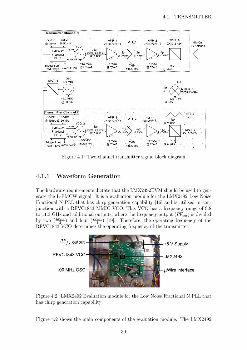
4.1. TRANSMITTER
Figure 4.1: Two channel transmitter signal block diagram
4.1.1 Waveform Generation
The hardware requirements dictate that the LMX2492EVM should be used to gen-erate the L-FMCW signal. It is a evaluation module for the LMX2492 Low NoiseFractional N PLL that has chirp generation capability [16] and is utilised in con-junction with a RFVC1843 MMIC VCO. This VCO has a frequency range of 9.8to 11.3 GHz and additional outputs, where the frequency output (RFout) is dividedby two (RFout
2) and four (RFout
4) [19]. Therefore, the operating frequency of the
RFVC1843 VCO determines the operating frequency of the transmitter.
Figure 4.2: LMX2492 Evaluation module for the Low Noise Fractional N PLL thathas chirp generation capability
Figure 4.2 shows the main components of the evaluation module. The LMX2492
39

4.1. TRANSMITTER
controls the output of the VCO by providing a tuning voltage that is in range of 0to 4.8 Volts. However, the VCO tuning voltage has a range of 0 to 15 Volts, hencethe full range that the VCO can provide is not accessible.
Furthermore, the specified frequency range of the LMX2492EVM is in the rangeof 9.4 to 10.1 GHz [20] for the undivided output channel, 4.7 to 5.05 GHz forthe RFout
2output and 2.35 to 2.525 GHz for the RFout
4output. As the system is
specified to operate at S-Band, the output of interest is the RFout4
. The maximumsignal bandwidth of that output channel is 175 MHz, which satisfies the bandwidthrequirements, as stated in Section 3.2.1.
It has to be noted that the specified operating frequency ranges for the evaluationboards and the VCO differ, this can be explained by referring to Figure 4.3(a),where the Frequency versus Tuning voltage of the undivided VCO output is shown.It can be seen that the frequency range from 9.8 to 11.3 GHz has a linear responseto the tuning voltage, where as the region in the frequency band below includ-ing the proposed 9.4 to 10.1 GHz, is non-linear. The same applies to the divideby four, RFout
4, output, as shown in Figure 4.3(b). Hence, the evaluation module
operates in the non-linear region of the VCO.
In order to compensate for the non-linearity, the PLL and VCO are connected ina closed loop configuration. This configuration allows a tuning voltage, which isproduced by the PLL, to be varied in accordance with the non-linear frequency-voltage response of the VCO and ensure that the output frequency ramp is linear,as described in Appendix B.1.1.
(a) Frequency versus Tuning voltage relationship forthe undivided (RFout) VCO output
(b) Frequency versus Tuning voltage relationship forthe divided by four (RFout
4 ) VCO output
Figure 4.3: Frequency versus Tuning voltage relationship of the RFVC1843VCO [19]
The power output of the VCO at the RFout4
channel, is defined to be -2 dBm, however,one also needs to consider the possible losses that may occur in the transmissionline that connect the given output to the SMA connector at the edge of the PrintedCircuit Board (PCB).
In addition to that, the default configuration of the evaluation board has a 6 dB
40
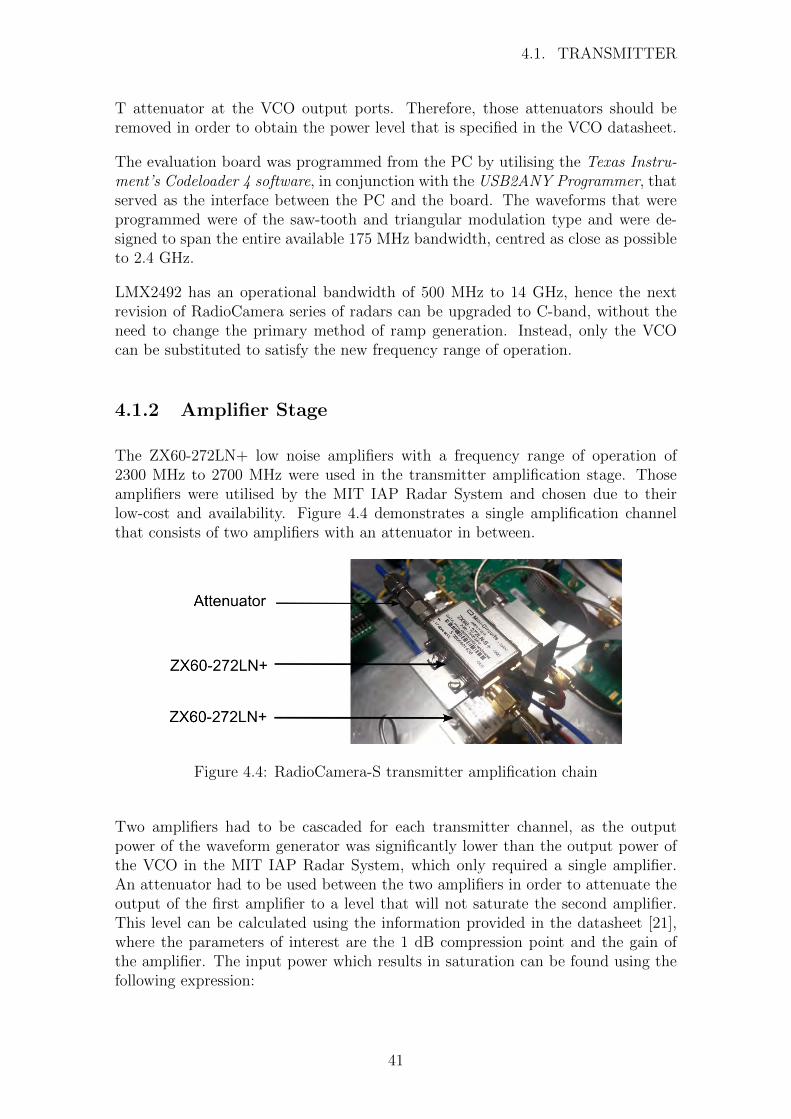
4.1. TRANSMITTER
T attenuator at the VCO output ports. Therefore, those attenuators should beremoved in order to obtain the power level that is specified in the VCO datasheet.
The evaluation board was programmed from the PC by utilising the Texas Instru-ment’s Codeloader 4 software, in conjunction with the USB2ANY Programmer, thatserved as the interface between the PC and the board. The waveforms that wereprogrammed were of the saw-tooth and triangular modulation type and were de-signed to span the entire available 175 MHz bandwidth, centred as close as possibleto 2.4 GHz.
LMX2492 has an operational bandwidth of 500 MHz to 14 GHz, hence the nextrevision of RadioCamera series of radars can be upgraded to C-band, without theneed to change the primary method of ramp generation. Instead, only the VCOcan be substituted to satisfy the new frequency range of operation.
4.1.2 Amplifier Stage
The ZX60-272LN+ low noise amplifiers with a frequency range of operation of2300 MHz to 2700 MHz were used in the transmitter amplification stage. Thoseamplifiers were utilised by the MIT IAP Radar System and chosen due to theirlow-cost and availability. Figure 4.4 demonstrates a single amplification channelthat consists of two amplifiers with an attenuator in between.
Figure 4.4: RadioCamera-S transmitter amplification chain
Two amplifiers had to be cascaded for each transmitter channel, as the outputpower of the waveform generator was significantly lower than the output power ofthe VCO in the MIT IAP Radar System, which only required a single amplifier.An attenuator had to be used between the two amplifiers in order to attenuate theoutput of the first amplifier to a level that will not saturate the second amplifier.This level can be calculated using the information provided in the datasheet [21],where the parameters of interest are the 1 dB compression point and the gain ofthe amplifier. The input power which results in saturation can be found using thefollowing expression:
41
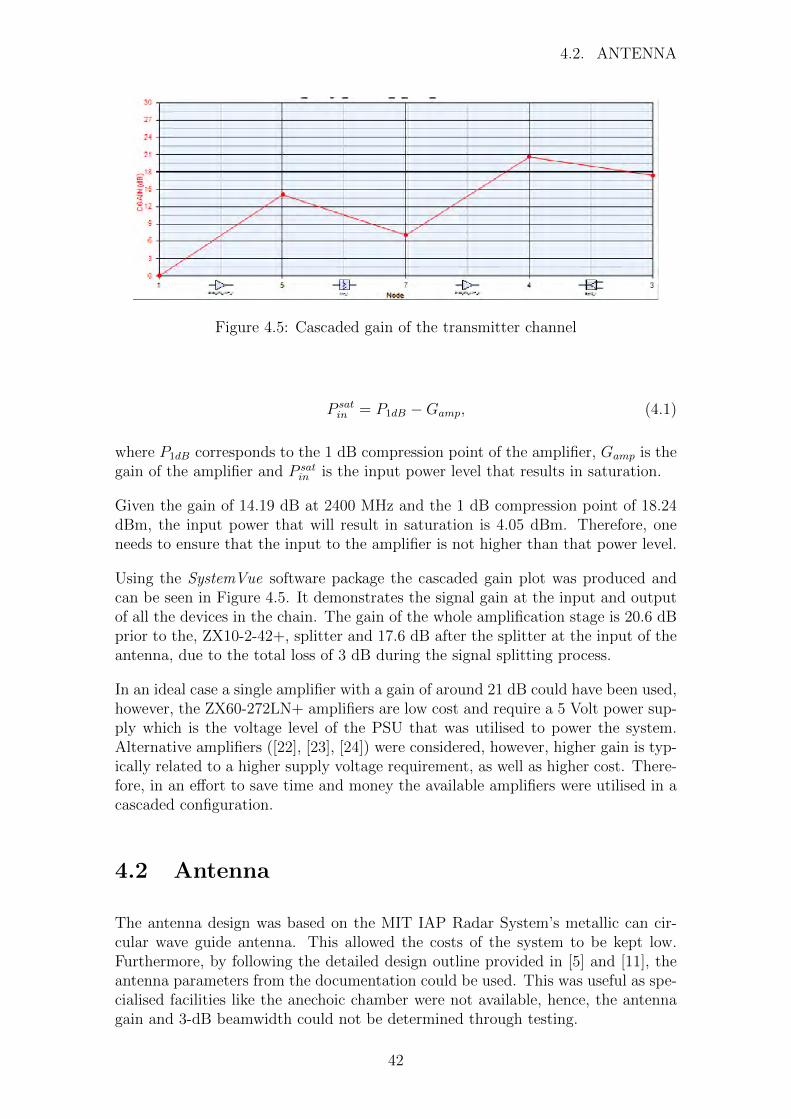
4.2. ANTENNA
Figure 4.5: Cascaded gain of the transmitter channel
P satin = P1dB −Gamp, (4.1)
where P1dB corresponds to the 1 dB compression point of the amplifier, Gamp is thegain of the amplifier and P sat
in is the input power level that results in saturation.
Given the gain of 14.19 dB at 2400 MHz and the 1 dB compression point of 18.24dBm, the input power that will result in saturation is 4.05 dBm. Therefore, oneneeds to ensure that the input to the amplifier is not higher than that power level.
Using the SystemVue software package the cascaded gain plot was produced andcan be seen in Figure 4.5. It demonstrates the signal gain at the input and outputof all the devices in the chain. The gain of the whole amplification stage is 20.6 dBprior to the, ZX10-2-42+, splitter and 17.6 dB after the splitter at the input of theantenna, due to the total loss of 3 dB during the signal splitting process.
In an ideal case a single amplifier with a gain of around 21 dB could have been used,however, the ZX60-272LN+ amplifiers are low cost and require a 5 Volt power sup-ply which is the voltage level of the PSU that was utilised to power the system.Alternative amplifiers ([22], [23], [24]) were considered, however, higher gain is typ-ically related to a higher supply voltage requirement, as well as higher cost. There-fore, in an effort to save time and money the available amplifiers were utilised in acascaded configuration.
4.2 Antenna
The antenna design was based on the MIT IAP Radar System’s metallic can cir-cular wave guide antenna. This allowed the costs of the system to be kept low.Furthermore, by following the detailed design outline provided in [5] and [11], theantenna parameters from the documentation could be used. This was useful as spe-cialised facilities like the anechoic chamber were not available, hence, the antennagain and 3-dB beamwidth could not be determined through testing.
42

4.2. ANTENNA
Figure 4.6: Circular waveguide antenna design parameters
4.2.1 Design Procedure
In order to successfully implement a circular wave guide antenna design, the pa-rameters shown in Figure 4.6 need to be chosen based on the required frequencyband of operation and a suitable mode of electromagnetic propagation.
The mode of signal propagation through the waveguide that was chosen is theTE11 circular waveguide mode. In order for other modes of propagation to notinterfere, a 100 mm diameter (D) is chosen for the circular waveguide. Given thediameter, the TE11 circular waveguide mode cut-off wavelength is found to be 170mm, which corresponds to a cut-off frequency of 1.8 GHz [11]. TE21 and TE01modes of propagation have cut-off frequencies at 2.9 and 3.6 GHz, respectively,which makes the above mentioned waveguide diameter suitable for operation in the2.4 GHz range.
As RadioCamera-S transmits a signal that is centred at the frequency of 2.4125GHz, which corresponds to the wavelength (λ) of 124 mm, the antenna’s probeneeds to be one quarter wavelength in order to excite the TE11 mode, which isapproximately 31 mm.
Another important parameter that places a requirement on the antenna design isimpedance matching, which determines the amount of power that is transferred. Inorder to achieve a satisfactory impedance match the position of the probe needsto be a quarter of the guide wavelength from the back wall of the waveguide [25].Therefore, given a guide wavelength (λg) of 185 mm at 2.4 GHz, the probe needsto be positioned 46 mm from the back wall of the waveguide.
Figure 4.7 shows the RadioCamera-S antennas, that were produced according tothe above requirements.
43
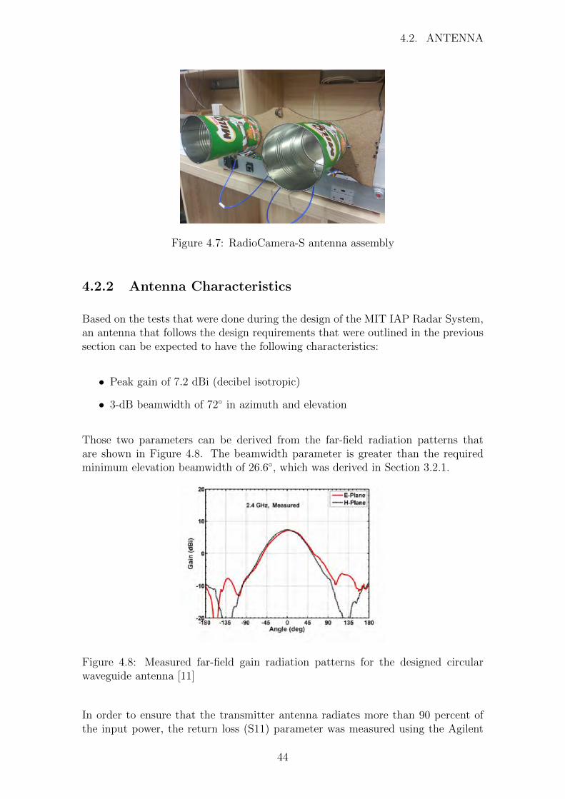
4.2. ANTENNA
Figure 4.7: RadioCamera-S antenna assembly
4.2.2 Antenna Characteristics
Based on the tests that were done during the design of the MIT IAP Radar System,an antenna that follows the design requirements that were outlined in the previoussection can be expected to have the following characteristics:
• Peak gain of 7.2 dBi (decibel isotropic)
• 3-dB beamwidth of 72◦ in azimuth and elevation
Those two parameters can be derived from the far-field radiation patterns thatare shown in Figure 4.8. The beamwidth parameter is greater than the requiredminimum elevation beamwidth of 26.6◦, which was derived in Section 3.2.1.
Figure 4.8: Measured far-field gain radiation patterns for the designed circularwaveguide antenna [11]
In order to ensure that the transmitter antenna radiates more than 90 percent ofthe input power, the return loss (S11) parameter was measured using the Agilent
44

4.2. ANTENNA
E5071B Network Analyser that was calibrated using Agilent’s 85033E CalibrationKit. The band of interest is 2.3 GHz to 2.5 GHz, where the return loss should beless or equal to -10 dB in order to ensure that the required amount of power istransmitted. This can be shown by first calculating the reflected power (Pr) usingthe following equation:
Pr = 10Return Loss
10 , (4.2)
where if a return loss of -10 dB is achieved Pr is equal to 0.1. The percentage oftransmitted power (Ptx)can then be calculated using Equation 4.3 [26].
Pt = 1− Pr, (4.3)
which results in Pt equal to 0.9 or 90 percent. The return loss measurement of thetransmitter antenna can be seen in Figure 4.9, which also shows that the bandwidthof the antenna is 2.31 GHz to 2.76 GHz.
Figure 4.9: Transmitter antenna return loss measurement
The return loss of the receiver antenna was also measured and utilised for thepurpose of tuning the antenna to the correct frequency band. The return loss plotfor the receiver antenna can be seen in Figure 4.10, which shows that the bandwidthof the receiver’s antenna is 2.18 GHz to 2.52 GHz wide.
Due to the fact that a dedicated antenna is used for the transmitter and for thereceiver, the isolation between the antennas in this configuration, determines theisolation between the transmitter and the receiver channels of the radar, as well
45
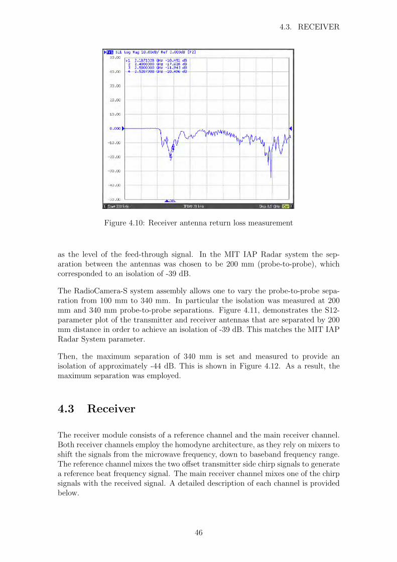
4.3. RECEIVER
Figure 4.10: Receiver antenna return loss measurement
as the level of the feed-through signal. In the MIT IAP Radar system the sep-aration between the antennas was chosen to be 200 mm (probe-to-probe), whichcorresponded to an isolation of -39 dB.
The RadioCamera-S system assembly allows one to vary the probe-to-probe sepa-ration from 100 mm to 340 mm. In particular the isolation was measured at 200mm and 340 mm probe-to-probe separations. Figure 4.11, demonstrates the S12-parameter plot of the transmitter and receiver antennas that are separated by 200mm distance in order to achieve an isolation of -39 dB. This matches the MIT IAPRadar System parameter.
Then, the maximum separation of 340 mm is set and measured to provide anisolation of approximately -44 dB. This is shown in Figure 4.12. As a result, themaximum separation was employed.
4.3 Receiver
The receiver module consists of a reference channel and the main receiver channel.Both receiver channels employ the homodyne architecture, as they rely on mixers toshift the signals from the microwave frequency, down to baseband frequency range.The reference channel mixes the two offset transmitter side chirp signals to generatea reference beat frequency signal. The main receiver channel mixes one of the chirpsignals with the received signal. A detailed description of each channel is providedbelow.
46

4.3. RECEIVER
Figure 4.11: Antenna isolation with a 200 mm probe-to-probe separation
Figure 4.12: Antenna isolation with a 340 mm probe-to-probe separation
4.3.1 Receiver Reference Channel
The reference channel is a product of the two offset ramp signals and consists of aZX05-43MH+ mixer and a VLFX-105 lowpass filter, with the Red Pitaya which isused to digitise the signal. Those components, as well as the signal levels can beseen in Figure 4.13.
47
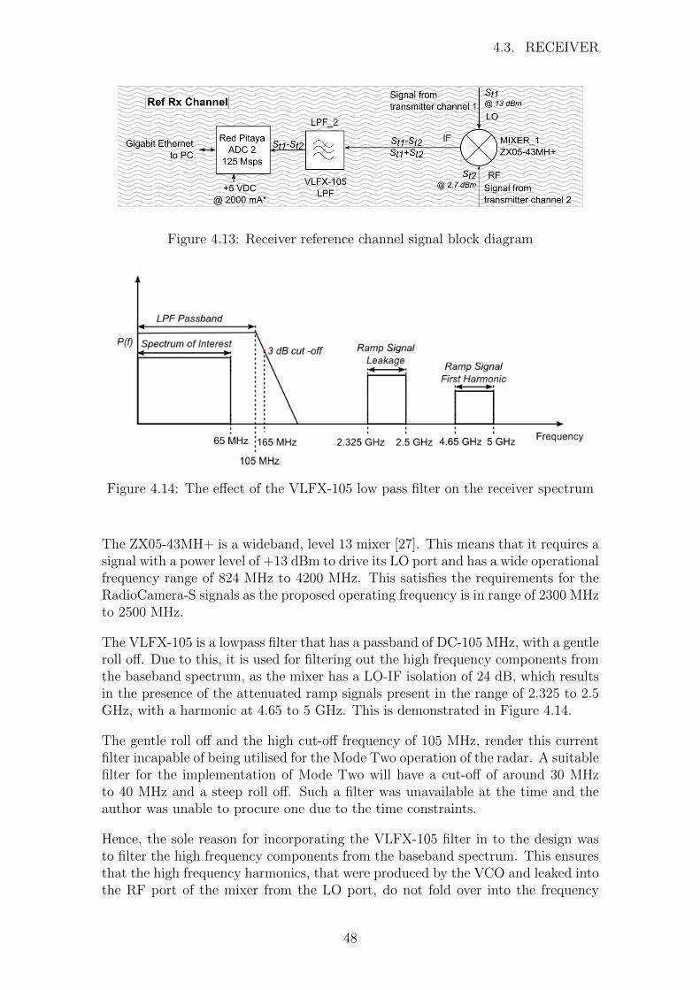
4.3. RECEIVER
Figure 4.13: Receiver reference channel signal block diagram
Figure 4.14: The effect of the VLFX-105 low pass filter on the receiver spectrum
The ZX05-43MH+ is a wideband, level 13 mixer [27]. This means that it requires asignal with a power level of +13 dBm to drive its LO port and has a wide operationalfrequency range of 824 MHz to 4200 MHz. This satisfies the requirements for theRadioCamera-S signals as the proposed operating frequency is in range of 2300 MHzto 2500 MHz.
The VLFX-105 is a lowpass filter that has a passband of DC-105 MHz, with a gentleroll off. Due to this, it is used for filtering out the high frequency components fromthe baseband spectrum, as the mixer has a LO-IF isolation of 24 dB, which resultsin the presence of the attenuated ramp signals present in the range of 2.325 to 2.5GHz, with a harmonic at 4.65 to 5 GHz. This is demonstrated in Figure 4.14.
The gentle roll off and the high cut-off frequency of 105 MHz, render this currentfilter incapable of being utilised for the Mode Two operation of the radar. A suitablefilter for the implementation of Mode Two will have a cut-off of around 30 MHzto 40 MHz and a steep roll off. Such a filter was unavailable at the time and theauthor was unable to procure one due to the time constraints.
Hence, the sole reason for incorporating the VLFX-105 filter in to the design wasto filter the high frequency components from the baseband spectrum. This ensuresthat the high frequency harmonics, that were produced by the VCO and leaked intothe RF port of the mixer from the LO port, do not fold over into the frequency
48

4.3. RECEIVER
Figure 4.15: Receiver main channel signal block diagram
spectrum of interest when the ADC samples the received signal.
As the reference receiver channel only consists of two components, the input satu-ration point is determined by the mixer. Hence, the RF input of the mixer mustnot be higher than 9 dBm in order to avoid saturating the channel.
It has to be noted that it is good practice to operate atleast 5 dB below this point.Hence, if an input of about 4 dBm is fed to the RF port, the output at the IF portshould be approximately -2.3 dBm, as the mixer has a typical conversion loss of 6.3dB.
4.3.2 Receiver Main Channel
The main receiver channel, consists of a ZX60-272LN+ LNA, ZX05-43MH+ mixer,LMH6521 IF amplifier, VLFX-105 lowpass filter and the Red Pitaya board fordigitising the signal. Figure 4.15 demonstrates the signal block diagram.
The analysis of the main receiver channel entails the derivation of the input satu-ration point, the cascaded Noise Figure (NF), sensitivity and the dynamic range,which are carried out in following sections.
Main Channel Input Saturation Analysis
In order to ensure that the receiver is not saturated, an analysis of the receivercomponent properties needs to be carried out and the saturation power of eachcomponent needs to be determined. Table 4.1 summarises the gain, conversionlosses, insertion losses, as well as the 1 dB compression points of the main receiverchannel components, which will be used to determine the receiver saturation point.
49
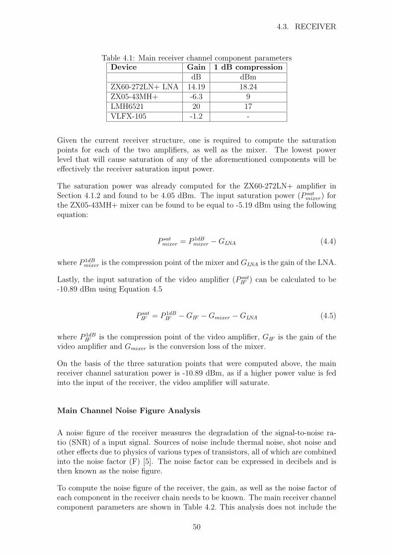
4.3. RECEIVER
Table 4.1: Main receiver channel component parametersDevice Gain 1 dB compression
dB dBmZX60-272LN+ LNA 14.19 18.24ZX05-43MH+ -6.3 9LMH6521 20 17VLFX-105 -1.2 -
Given the current receiver structure, one is required to compute the saturationpoints for each of the two amplifiers, as well as the mixer. The lowest powerlevel that will cause saturation of any of the aforementioned components will beeffectively the receiver saturation input power.
The saturation power was already computed for the ZX60-272LN+ amplifier inSection 4.1.2 and found to be 4.05 dBm. The input saturation power (P sat
mixer) forthe ZX05-43MH+ mixer can be found to be equal to -5.19 dBm using the followingequation:
P satmixer = P 1dB
mixer −GLNA (4.4)
where P 1dBmixer is the compression point of the mixer and GLNA is the gain of the LNA.
Lastly, the input saturation of the video amplifier (P satIF ) can be calculated to be
-10.89 dBm using Equation 4.5
P satIF = P 1dB
IF −GIF −Gmixer −GLNA (4.5)
where P 1dBIF is the compression point of the video amplifier, GIF is the gain of the
video amplifier and Gmixer is the conversion loss of the mixer.
On the basis of the three saturation points that were computed above, the mainreceiver channel saturation power is -10.89 dBm, as if a higher power value is fedinto the input of the receiver, the video amplifier will saturate.
Main Channel Noise Figure Analysis
A noise figure of the receiver measures the degradation of the signal-to-noise ra-tio (SNR) of a input signal. Sources of noise include thermal noise, shot noise andother effects due to physics of various types of transistors, all of which are combinedinto the noise factor (F) [5]. The noise factor can be expressed in decibels and isthen known as the noise figure.
To compute the noise figure of the receiver, the gain, as well as the noise factor ofeach component in the receiver chain needs to be known. The main receiver channelcomponent parameters are shown in Table 4.2. This analysis does not include the
50

4.3. RECEIVER
losses associated with the cable that connects the receiver antenna to the receiveritself. Hence, the following analysis determines the noise figure of the radar receiverand not that of the whole radar system.
Table 4.2: Main receiver channel component parametersDevice Gain Noise Figure
dB dBZX60-272LN+ 14.19 1.1ZX05-43MH+ -6.3 6.3LMH6521 20 7.3VLFX-105 -1.2 1.2
The noise figure of the receiver can be calculated using Equation 4.6, where FLNA,Fmixer, FIF , FLPF are the noise factors of the LNA, mixer, IF amplifier and the lowpass filter respectively. GLNA corresponds to the gain of the LNA, Gmixer is theconversion loss that is associated with the mixer and GIF is the gain of the videoamplifier. Those values are all required to be expressed in linear units. Hence,taking into considerations the component parameters and by utilising the providedequation, the main receiver channel noise figure is found to be 5.14 dB.
NF = 10×(FLNA +
Fmixer − 1
GLNA
+FIF − 1
GLNAGmixer
+FLPF − 1
GLNAGmixerGIF
)(4.6)
A more detailed description of the noise figure is provided in Appendix B.3.1.
Receiver Sensitivity
Receiver sensitivity defines the weakest signal that can be detected by the radarreceiver. This is also known as the Minimum Detectable Signal (MDS) and ismeasured in dBm [13] [5]. The noise that is associated with the radar receiveressentially sets the limit on the MDS, as is shown by Equation B.20.
MDS = 10log10
(kT0
1mW
)+NFsys + 10log(BWrec) + SNRout, (4.7)
where k is the Boltzmann’s constant (1.38×10⁻²³ joules/Kelvin), T0 is the standardtemperature equal to 290◦, BWrec is the receiver bandwidth (Hz) and SNRout is theminimum required SNR for detection.
Hence, in order to calculate the MDS, the receiver bandwidth can be approximatedto be 62.5 MHz, based on the sampling rate of the Red Pitaya and a signal-to-noiseratio that can be set to 13.4 dB, which corresponds to the gold standard of radar
51

4.4. SYSTEM HOUSING
performance providing the probability of detection of 95 percent and a probabilityof false alarm of 10−6 [5]. Finally, given the noise figure of 5.14 dB, the MDS ofthe RadioCamera-S receiver can be approximated to be -77.5 dBm. Similarly tothe noise figure analysis, this receiver sensitivity analysis derives the MDS for theRadioCamera-S receiver and not the radar system. This occurs because the powerloss of the cable that attaches the receiver antenna to the RadioCamera-S receiveris not taken into consideration in this analysis.
Receiver Dynamic Range
The dynamic range of the receiver is defined to be the difference between the peaksignal that can be processed by the receiver without the receiver saturating and theMDS. Additionally, this dynamic range should be facilitated by the ADC that wasused to digitise the signal.
The maximum signal that the receiver can process was computed for the RadioCamera-S receiver and found to be approximately -10.89 dBm. The MDS of the receiverwas found to be -77.48 dBm. Therefore, the dynamic range of the receiver is 66.59dB. This dynamic range should be able to be processed by the receiver as it is lessthan the expected theoretical maximum dynamic range of Red Pitaya’s ADC (86.7dB, as mentioned in Section 3.1.4).
4.4 System Housing
The system housing that was required to provide a base for the three system moduleswas designed in accordance with the following requirements:
• Enable easy access to the components for debugging
• Provide a neat layout and wiring distribution
• Portable housing that can be easily transported
• Neat front panel design for external connections
• Aluminium body in order to provide a common ground for the components
All the above requirements were implemented in a system housing, which was de-signed using SolidWorks CAD software package. The complete system assemblyis shown in Figure 4.16, which demonstrates the placement of the main systemcomponents.
52
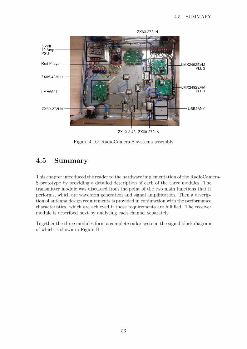
4.5. SUMMARY
Figure 4.16: RadioCamera-S systema assembly
4.5 Summary
This chapter introduced the reader to the hardware implementation of the RadioCamera-S prototype by providing a detailed description of each of the three modules. Thetransmitter module was discussed from the point of the two main functions that itperforms, which are waveform generation and signal amplification. Then a descrip-tion of antenna design requirements is provided in conjunction with the performancecharacteristics, which are achieved if those requirements are fulfilled. The receivermodule is described next by analysing each channel separately.
Together the three modules form a complete radar system, the signal block diagramof which is shown in Figure B.1.
53
Chapter 5
RadioCamera-S Testing andResults
The test procedures that are outlined in this chapter relate to the performance anal-ysis of the transmitter and the receiver modules, as well as, the performance of thecompletely integrated system. The transmitter tests can be seen in Section 5.1, withthe receiver module testing provided in Section 5.2. The system tests are dividedinto delay-line tests in Section 5.3 and the fully integrated system tests as describedin Section 5.4.
Each section aims to describe the testing procedures, demonstrate the results andprovide a brief discussion.
5.1 Transmitter Testing
The transmitter tests are divided into the waveform generation tests and the am-plification stage power level verification.
5.1.1 Waveform Generation
In order for RadioCamera-S to operate as a FMCW ranging and imaging radar, theoutput of the waveform generator is required to span the bandwidth of interest andfollow a correct modulation scheme. As was proposed in Section 3.2.1 and 3.2.2,the two waveforms that will be examined are:
Waveform 1 - 175 MHz bandwidth, 50 µs up ramp with a 25 µs down ramp
Waveform 2 - 175 MHz bandwidth, 100 µs up ramp with a 25 µs down ramp
The output of the LMX2492EVM module is connected to the Agilent Technolo-gies Field Fox Spectrum Analyser in order to examine the spectrum of the output
54
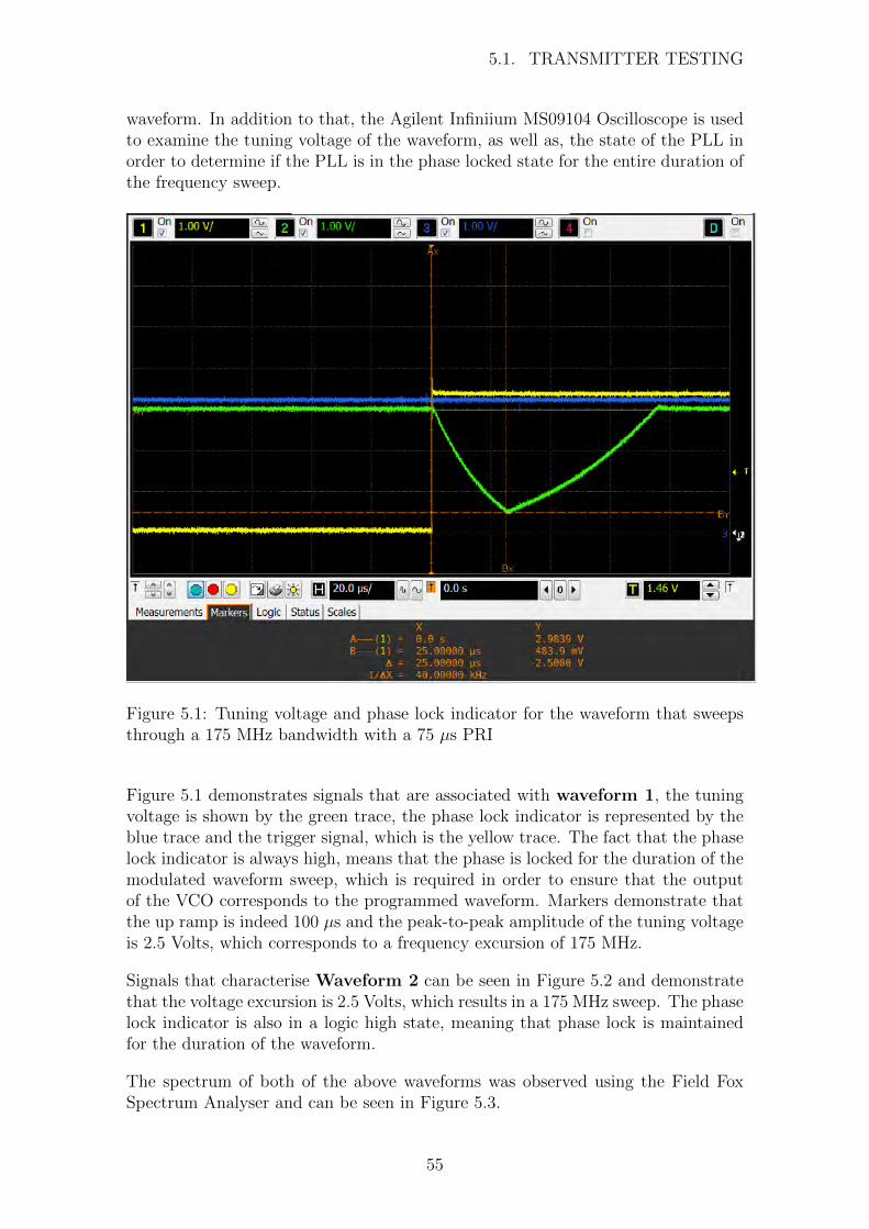
5.1. TRANSMITTER TESTING
waveform. In addition to that, the Agilent Infiniium MS09104 Oscilloscope is usedto examine the tuning voltage of the waveform, as well as, the state of the PLL inorder to determine if the PLL is in the phase locked state for the entire duration ofthe frequency sweep.
Figure 5.1: Tuning voltage and phase lock indicator for the waveform that sweepsthrough a 175 MHz bandwidth with a 75 µs PRI
Figure 5.1 demonstrates signals that are associated with waveform 1, the tuningvoltage is shown by the green trace, the phase lock indicator is represented by theblue trace and the trigger signal, which is the yellow trace. The fact that the phaselock indicator is always high, means that the phase is locked for the duration of themodulated waveform sweep, which is required in order to ensure that the outputof the VCO corresponds to the programmed waveform. Markers demonstrate thatthe up ramp is indeed 100 µs and the peak-to-peak amplitude of the tuning voltageis 2.5 Volts, which corresponds to a frequency excursion of 175 MHz.
Signals that characterise Waveform 2 can be seen in Figure 5.2 and demonstratethat the voltage excursion is 2.5 Volts, which results in a 175 MHz sweep. The phaselock indicator is also in a logic high state, meaning that phase lock is maintainedfor the duration of the waveform.
The spectrum of both of the above waveforms was observed using the Field FoxSpectrum Analyser and can be seen in Figure 5.3.
55
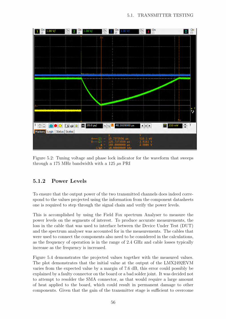
5.1. TRANSMITTER TESTING
Figure 5.2: Tuning voltage and phase lock indicator for the waveform that sweepsthrough a 175 MHz bandwidth with a 125 µs PRI
5.1.2 Power Levels
To ensure that the output power of the two transmitted channels does indeed corre-spond to the values projected using the information from the component datasheetsone is required to step through the signal chain and verify the power levels.
This is accomplished by using the Field Fox spectrum Analyser to measure thepower levels on the segments of interest. To produce accurate measurements, theloss in the cable that was used to interface between the Device Under Test (DUT)and the spectrum analyser was accounted for in the measurements. The cables thatwere used to connect the components also need to be considered in the calculations,as the frequency of operation is in the range of 2.4 GHz and cable losses typicallyincrease as the frequency is increased.
Figure 5.4 demonstrates the projected values together with the measured values.The plot demonstrates that the initial value at the output of the LMX2492EVMvaries from the expected value by a margin of 7.6 dB, this error could possibly beexplained by a faulty connector on the board or a bad solder joint. It was decided notto attempt to resolder the SMA connector, as that would require a large amountof heat applied to the board, which could result in permanent damage to othercomponents. Given that the gain of the transmitter stage is sufficient to overcome
56
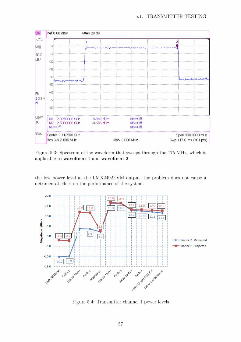
5.1. TRANSMITTER TESTING
Figure 5.3: Spectrum of the waveform that sweeps through the 175 MHz, which isapplicable to waveform 1 and waveform 2
the low power level at the LMX2492EVM output, the problem does not cause adetrimental effect on the performance of the system.
Figure 5.4: Transmitter channel 1 power levels
57

5.2. RECEIVER POWER LEVEL VERIFICATION
The rest of the power levels are sufficiently close to the projected values, except forthe output of the front-panel connector and the cable connecting the antenna tothe output port. These two values are down by approximately 1 dB, which can beattributed to measurement error, as the Spectrum Analyser typically has a +/- 0.5dB amplitude accuracy. Another possible cause for this fault could be damage tothe cable, that was caused by excessive bending.
Figure 5.5: Transmitter channel 2 power levels
Transmitter channel 2 power levels can be examined in Figure 5.5, where the worstdisparity is equal to 0.7 dB, which occurs at the output of the first amplifier. Thiscan be explained by the fact that the gain of the amplifier is not flat across the wholeband and the projected value could be off by a small amount. That, in conjunctionwith the measurement uncertainty of the equipment could be the result of thedisparity.
Overall the power levels conform with the expected values and the outputs aresufficiently high to drive the LO ports of the mixers and provide the needed powerto the transmitter antenna.
5.2 Receiver Power Level Verification
The power levels of the two receiver channels were analysed using a similar procedureto that outlined in Section 5.1.2.
The input power to the receiver was set to a power level of -26.2 dBm. Thiscorresponds to the maximum output power of the transmitter with the antenna
58

5.3. DELAY-LINE TESTS
isolation added to it, which is the power level of the direct coupling, or feed-throughsignal.
The actual calculation determined the maximum signal to be at a level of -27.5dBm, however, as the attenuators that were used, had a +/- 0.5 dB variance theresultant input signal was higher than expected. This explains the disparity in theprojected and measured values in Figure 5.6.
Figure 5.6: Main receiver channel power levels
The power levels associated with the reference channel of the receiver can be exam-ined in Figure 5.7. The projected values conform to that of the measured ones, itshould be noted that the loss associated with the cable that connects the spectrumanalyser with the DUT reduces greatly at baseband frequencies, this was accountedfor, for components at the IF output port of the mixer.
The projected values conform to the measured values for the receiver channels. Theexpected power levels at the input of the signal digitiser are 0.4 dBm for the mainchannel and -3.3 for the reference channel. The lower power level of the referencechannel can be tolerated, as there are no signal returns that can interfere with it,as the reference channel is a product of two internally generated waveforms.
5.3 Delay-Line Tests
The delay-line test makes use of two LMR400 cables that have a 50 ohm impedance,with the associated delays of:
Cable 1 - 59.96 ns
59
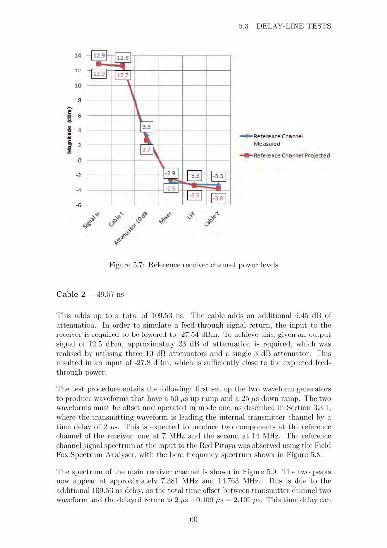
5.3. DELAY-LINE TESTS
Figure 5.7: Reference receiver channel power levels
Cable 2 - 49.57 ns
This adds up to a total of 109.53 ns. The cable adds an additional 6.45 dB ofattenuation. In order to simulate a feed-through signal return, the input to thereceiver is required to be lowered to -27.54 dBm. To achieve this, given an outputsignal of 12.5 dBm, approximately 33 dB of attenuation is required, which wasrealised by utilising three 10 dB attenuators and a single 3 dB attenuator. Thisresulted in an input of -27.8 dBm, which is sufficiently close to the expected feed-through power.
The test procedure entails the following: first set up the two waveform generatorsto produce waveforms that have a 50 µs up ramp and a 25 µs down ramp. The twowaveforms must be offset and operated in mode one, as described in Section 3.3.1,where the transmitting waveform is leading the internal transmitter channel by atime delay of 2 µs. This is expected to produce two components at the referencechannel of the receiver, one at 7 MHz and the second at 14 MHz. The referencechannel signal spectrum at the input to the Red Pitaya was observed using the FieldFox Spectrum Analyser, with the beat frequency spectrum shown in Figure 5.8.
The spectrum of the main receiver channel is shown in Figure 5.9. The two peaksnow appear at approximately 7.381 MHz and 14.763 MHz. This is due to theadditional 109.53 ns delay, as the total time offset between transmitter channel twowaveform and the delayed return is 2 µs +0.109 µs = 2.109 µs. This time delay can
60
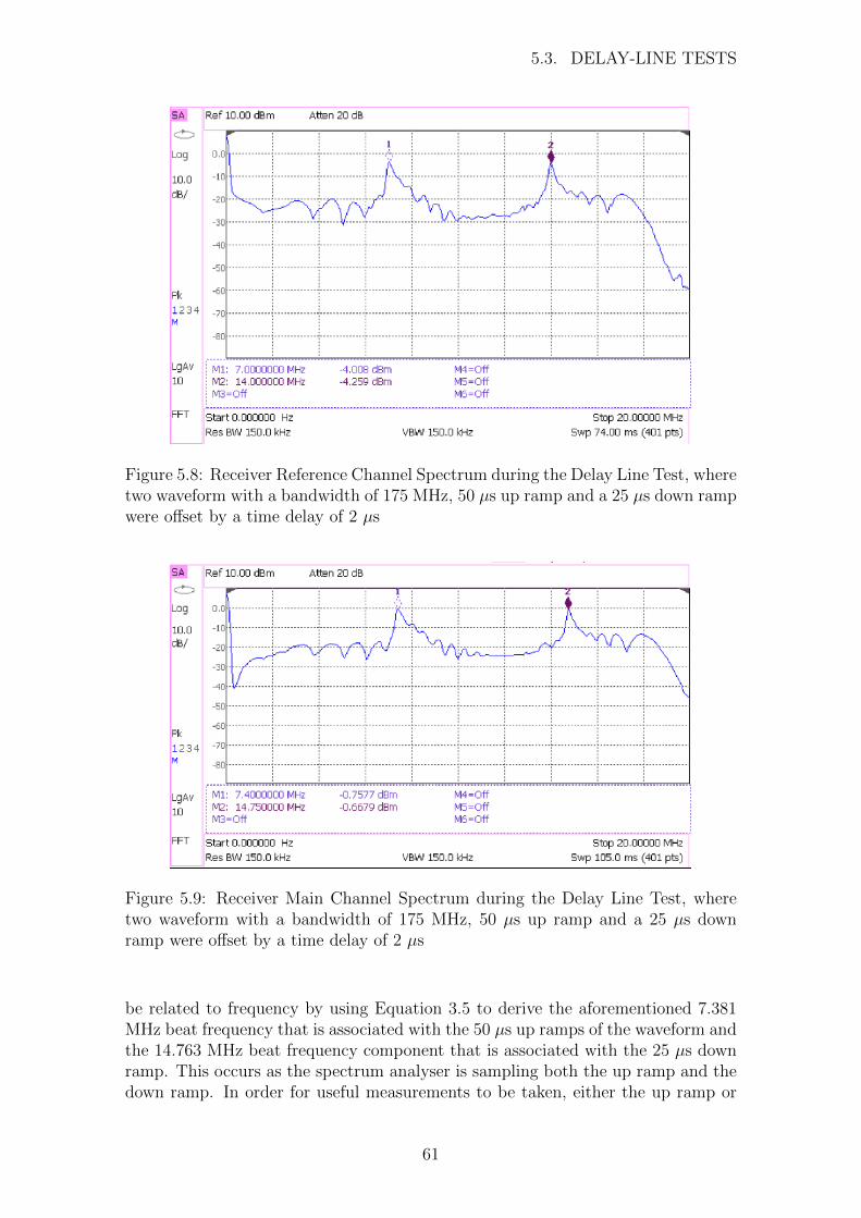
5.3. DELAY-LINE TESTS
Figure 5.8: Receiver Reference Channel Spectrum during the Delay Line Test, wheretwo waveform with a bandwidth of 175 MHz, 50 µs up ramp and a 25 µs down rampwere offset by a time delay of 2 µs
Figure 5.9: Receiver Main Channel Spectrum during the Delay Line Test, wheretwo waveform with a bandwidth of 175 MHz, 50 µs up ramp and a 25 µs downramp were offset by a time delay of 2 µs
be related to frequency by using Equation 3.5 to derive the aforementioned 7.381MHz beat frequency that is associated with the 50 µs up ramps of the waveform andthe 14.763 MHz beat frequency component that is associated with the 25 µs downramp. This occurs as the spectrum analyser is sampling both the up ramp and thedown ramp. In order for useful measurements to be taken, either the up ramp or
61

5.4. INTEGRATED SYSTEM TESTS
the down ramp must be sampled. This can be achieved with the Red Pitaya, as isshown in Figure 5.10, where only the 50 µs up ramp is sampled, which results inthe absence of 14 and 14.763 MHz components from the spectrum.
Figure 5.10: Reference and Main Receiver Spectrums Acquired by the Red Pitaya,where two waveform with a bandwidth of 175 MHz, 50 µs up ramp and a 25 µsdown ramp were offset by a time delay of 2 µs and only the 50 µs up ramp wassampled
5.4 Integrated System Tests
The tests in this section aim to demonstrate that the radar can be operated in theFMCW ranging mode, as well as implement operation mode number one for thepurpose of the feed-through signal filtering.
The waveform that was used for the purpose of the tests has a bandwidth of 175MHz and a total PRI of 75 µs, with a up ramp of 50 µs and a down ramp of 25 µs.The part of the waveform that was digitised by the Red Pitaya is the down ramp.This was utilised due to the fact that a shorter sweep corresponds to a greaterspectral spread and as the scene is limited to 40 m, it is advantageous to spread thetargets as broadly as possible across the beat frequency spectrum.
The series of tests starts by obtaining a return from a scene without the presence ofa reference reflector. The scene is shown in Figure 5.11, which is a 40 m corridor.The transmitter is setup in a way that the transmitter channel 2 is lagging thewaveform at channel 1 by 560 ns. This places the feed-through component at 4MHz in the main receiver channel, with the reference channel having a peak of 3.93MHz. The raw signal returns can be seen in Figure 5.12.
A Matlab program is implemented to search for the peak in the reference channeland use it to determine the true range of the targets in the scene. The output of thisprocess is demonstrated in Figure 5.13, where the feed-through is the component
62

5.4. INTEGRATED SYSTEM TESTS
Figure 5.11: Test scene for the RadioCamera-S integration tests
Figure 5.12: The two receiver channels in the frequency domain
that has the highest power and a return from the far wall of the corridor can beseen at approximately 39 m.
Next, a trolley with a reflector, which can be seen in Figure 5.14, was placed at4.5 m, 16 m and 28.8 m away from the radar. The return signals were recordedand overlaid on a same graph, which can be seen in Figure 5.15, where the red plotshows the reflection when the trolley was placed at 4.5 m, the black plot shows thereturn when the trolley was located 16 m away from the radar and the blue plotcorresponds to the trolley located 28 m down the passage.
63

5.4. INTEGRATED SYSTEM TESTS
Figure 5.13: Receiver main channel Magnitude-Range plot
In most cases, unless the target is located very close to the radar the feed-throughcomponent is the most prominent signal in the spectrum, in order to reduce it, thecharacteristics of the video amplifier can be utilised. Figure 5.16 demonstrates theamplification profile, the markers show that if a component is placed at 1 MHz,the signal level will be approximately 3 dB lower than the component at 1.3 MHz,hence operation mode one can be utilised and the feed-through component can beplaced at 1 MHz by setting a 130 ns delay between the transmitted waveforms, withtransmitter channel 2 leading channel 1.
The results of this operation can be seen in Figure 5.17, where the blue plot cor-responds to the return signals if one places the components in the frequency bandwhere video amplifier has a flat gain response and the red plot corresponds to thecase when the feed-through is placed at 1 MHz.
The result of this manipulation also causes the nearby components to be attenuated,however, the overall effect results in a decrease in the dynamic range requirement,atleast by a factor of 4 dB. In an ideal case a highpass filter with a steep cut-offshould be used, but due to the fact that such a filter was unavailable during testing,the amplifier response was adapted to demonstrate the concept of the feed-throughremoval using the two-channel approach.
Lastly, the Range-Time-Intensity (RTI) plot was produced, which consists of 100
64
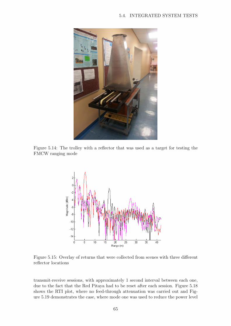
5.4. INTEGRATED SYSTEM TESTS
Figure 5.14: The trolley with a reflector that was used as a target for testing theFMCW ranging mode
Figure 5.15: Overlay of returns that were collected from scenes with three differentreflector locations
transmit-receive sessions, with approximately 1 second interval between each one,due to the fact that the Red Pitaya had to be reset after each session. Figure 5.18shows the RTI plot, where no feed-through attenuation was carried out and Fig-ure 5.19 demonstrates the case, where mode one was used to reduce the power level
65
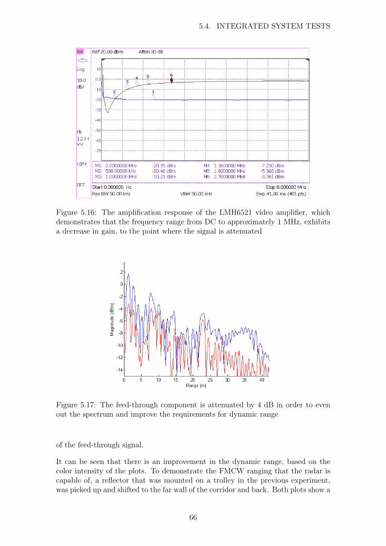
5.4. INTEGRATED SYSTEM TESTS
Figure 5.16: The amplification response of the LMH6521 video amplifier, whichdemonstrates that the frequency range from DC to approximately 1 MHz, exhibitsa decrease in gain, to the point where the signal is attenuated
Figure 5.17: The feed-through component is attenuated by 4 dB in order to evenout the spectrum and improve the requirements for dynamic range
of the feed-through signal.
It can be seen that there is an improvement in the dynamic range, based on thecolor intensity of the plots. To demonstrate the FMCW ranging that the radar iscapable of, a reflector that was mounted on a trolley in the previous experiment,was picked up and shifted to the far wall of the corridor and back. Both plots show a
66
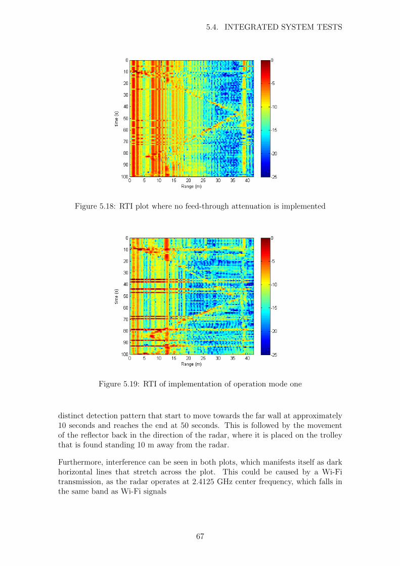
5.4. INTEGRATED SYSTEM TESTS
Figure 5.18: RTI plot where no feed-through attenuation is implemented
Figure 5.19: RTI of implementation of operation mode one
distinct detection pattern that start to move towards the far wall at approximately10 seconds and reaches the end at 50 seconds. This is followed by the movementof the reflector back in the direction of the radar, where it is placed on the trolleythat is found standing 10 m away from the radar.
Furthermore, interference can be seen in both plots, which manifests itself as darkhorizontal lines that stretch across the plot. This could be caused by a Wi-Fitransmission, as the radar operates at 2.4125 GHz center frequency, which falls inthe same band as Wi-Fi signals
67
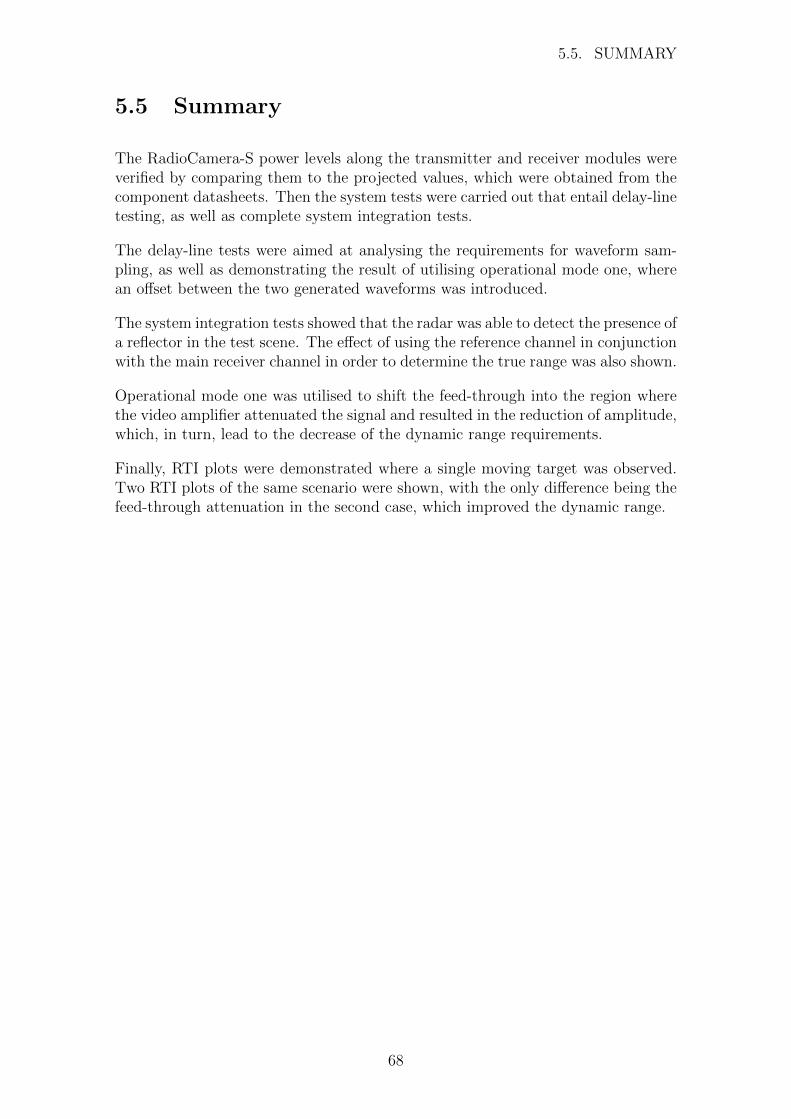
5.5. SUMMARY
5.5 Summary
The RadioCamera-S power levels along the transmitter and receiver modules wereverified by comparing them to the projected values, which were obtained from thecomponent datasheets. Then the system tests were carried out that entail delay-linetesting, as well as complete system integration tests.
The delay-line tests were aimed at analysing the requirements for waveform sam-pling, as well as demonstrating the result of utilising operational mode one, wherean offset between the two generated waveforms was introduced.
The system integration tests showed that the radar was able to detect the presence ofa reflector in the test scene. The effect of using the reference channel in conjunctionwith the main receiver channel in order to determine the true range was also shown.
Operational mode one was utilised to shift the feed-through into the region wherethe video amplifier attenuated the signal and resulted in the reduction of amplitude,which, in turn, lead to the decrease of the dynamic range requirements.
Finally, RTI plots were demonstrated where a single moving target was observed.Two RTI plots of the same scenario were shown, with the only difference being thefeed-through attenuation in the second case, which improved the dynamic range.
68
Chapter 6
Conclusions andRecommendations
6.1 Conclusions
In the context of hardware implementation, the RadioCamera-S prototype achievedthe following objectives:
• Operates in S-Band
• LMX2492EVM was used to generate custom L-FMCW waveforms
• Successfully implemented the LMH6521 IF amplifier in the main channel ofthe receiver
• Red Pitaya was used to trigger the waveform generator boards
• Red Pitaya was used to acquire data while using an external trigger to startacquisition
• Low-cost antennas were made and tested
Hence, it can be said that the hardware requirements were fulfilled.
The proposed airborne system geometry was analysed and the effect on the designparameters was discussed and a waveform type was proposed for the implementationin the airborne scenario. However, due to the many discrepancies between the futureairborne implementation which will operate in C-band, it was found problematic torelate the current prototype specification to the airborne scenario.
This resulted in a specification being developed for the ground based system only.The refined version of that specification can be seen in Table 6.1. Additional pa-rameters, which come as a result of testing, are added to the existing specification.
69
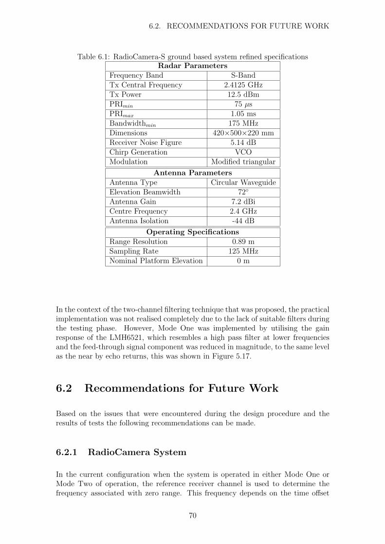
6.2. RECOMMENDATIONS FOR FUTURE WORK
Table 6.1: RadioCamera-S ground based system refined specificationsRadar Parameters
Frequency Band S-BandTx Central Frequency 2.4125 GHzTx Power 12.5 dBmPRImin 75 µsPRImax 1.05 msBandwidthmin 175 MHzDimensions 420×500×220 mmReceiver Noise Figure 5.14 dBChirp Generation VCOModulation Modified triangular
Antenna ParametersAntenna Type Circular WaveguideElevation Beamwidth 72◦
Antenna Gain 7.2 dBiCentre Frequency 2.4 GHzAntenna Isolation -44 dB
Operating SpecificationsRange Resolution 0.89 mSampling Rate 125 MHzNominal Platform Elevation 0 m
In the context of the two-channel filtering technique that was proposed, the practicalimplementation was not realised completely due to the lack of suitable filters duringthe testing phase. However, Mode One was implemented by utilising the gainresponse of the LMH6521, which resembles a high pass filter at lower frequenciesand the feed-through signal component was reduced in magnitude, to the same levelas the near by echo returns, this was shown in Figure 5.17.
6.2 Recommendations for Future Work
Based on the issues that were encountered during the design procedure and theresults of tests the following recommendations can be made.
6.2.1 RadioCamera System
In the current configuration when the system is operated in either Mode One orMode Two of operation, the reference receiver channel is used to determine thefrequency associated with zero range. This frequency depends on the time offset
70

6.2. RECOMMENDATIONS FOR FUTURE WORK
between the two ramp signals that are produced by the two waveform generators.Since the time offset is determined by the radar operator, there is no need to recordthis channel given that the two waveforms are triggered at the exact time that theoperator specified.
RadioCamera-S prototype was used to investigate the operation of the Red Pitaya,as well as the LMX2492 ramp generator module and the time delays that wereassociated with triggering the ramp generators. Therefore, the reference signal wassampled for verification of the zero range and to ensure that the Red Pitaya platformcould sample the two channels at the same time without a time delay between thetwo.
The future revisions of the RadioCamera system, could utilise the second channelto:
• Record a copy of the signal at the transmitter antenna to determine the timedelay due to the transmit antenna cable
• Interferometry, where by an additional receiver antenna will be added to thesetup. The de-ramped return of which could be sampled by the second channel
6.2.2 Transmitter
LMX2492EVM
The two waveform generators are currently synchronised using a single-ended 100MHz Oscillator. As the Red Pitaya requires a differential clock signal that utilisesthe LVDS standard and the waveform generator boards also can be clocked usinga differential clock source, it might be of interest to switch from the single-endedoscillator to a differential source that can provide a clock signal to all three devices,thereby keeping them synchronised.
Amplification stage
During the design process of RadioCamera-S, it was found that a single ZX60-272LN+ amplifier was not sufficient and as a result, two amplifiers were cascadedto provide sufficient gain. In order to improve on this a single amplifier can beutilised.
The amplifier is required to have a gain of approximately 21 dB. Additional con-straints are that the current setup operates from a 5 Volt PSU, should an amplifierthat has more gain and requires more power be chosen, the PSU that powers theRadioCamera-S prototype will have to be redesigned.
71
6.2. RECOMMENDATIONS FOR FUTURE WORK
6.2.3 Antenna
The isolation between the two antennas was measured to be approximately -44 dBwhen a maximum probe-to-probe separation was utilised. The methods of improv-ing the isolation through the use of Radar Absorbing Material (RAM) betweenthe antennas or alternatively the use of choke rings around the antennas could beinvestigated.
The antenna isolation determine the level of the feed-through signal, which thecurrent study aims to filter, if the isolation could be improved and the level of thesignal attenuated, the problem of filtering could be simplified.
6.2.4 Receiver
Filters
During the testing phase of this research project, low pass filters with a steep cut-off and a cut-off frequency in the order of 20 to 30 MHz, were unavailable. Hence,Mode Two for feed-through signal filtering was not implemented.
Furthermore, an actual high pass filter could also be tested and the two modesof filtering the signals out compared. The gain response of the video amplifierthat was used to demonstrate the operation of Mode One filtering technique, diddemonstrate, the attenuation of the feed-through signal by 4 dB, however, this hasto be implemented with a stand alone filter in order to see if the feed-through canbe filtered completely.
Red Pitaya
If the Red Pitaya will be used on future revisions of the RadioCamera radars it willneed to be able to:
• Program and send control signals to the LMX2492 ramp generator
• Store data on the SD card or on an alternative source
• Store data continuously (more than 16384 samples at a time)
• Control the gain on the LMH6521 video amplifier
Hence, the development of any of those aspects will be beneficial to the final designof the airborne FMCW imaging sensor.
72
Bibliography
[1] R. Smith, “Micro Synthetic Aperture Radar Using FM/CW Technology,”Master’s thesis, Brigham Young University, 2002.
[2] M. Duersch, “BYU Micro-SAR: A Very Small, Low-Power LFM-CW Syn-thetic Aperture Radar,” Master’s thesis, Brigham Young University, Decem-ber 2004.
[3] E. Zaugg, D. Hudson, and D. Long, “The BYU microSAR: A Small,Student-Built SAR for UAV Operation,” in Proceedings of the InternationalGeoscience and Remote Sensing Symposium, August 2006.
[4] M. Edwards et al., “MicroASAR: A Small, Robust LFM-CW SAR for Oper-ation on UAVs and Small Aircraft,” in Proceedings of the International Geo-science and Remote Sensing Symposium, July 2008.
[5] G. Charvat, Small and Short-Range Radar Systems. CRC Press, 2014.
[6] H. Griffiths, “New ideas in FM radar,” Electronics Communication Engineer-ing Journal, vol. 2, pp. 185–194, Oct 1990.
[7] E. Murphy and C. Slattery, “All About Direct Digital Synthesis,” August2004.
[8] Mini-Circuits, “Amplifier Terms Defined.” [Online].http://www.minicircuits.com/app/AN60-038.pdf [Accessed: 8 February2015], October 2010.
[9] M. Inggs and R. Lord, “Applications of Satellite Imaging Radar,” in SouthAfrican Institute of Electrical Engineering, 2000.
[10] M. Inggs and R. Lord, “Current Applications of Imaging Radar,” in Interna-tional Conference on Advanced Remote Sensing for Earth Observation Sys-tems, Techniques and Applications, vol. XXXVI-1/w12, May 2005.
[11] G. Charvat, A. Fenn, and B. Perry, “The MIT IAP radar course: Build aSmall Radar System Capable of Sensing Range, Doppler, and SyntheticAperture (SAR) Imaging,” in IEEE Radar Conference, 2012, May 2012.
[12] D. Thompson, D. Arnold, and D. Long, “YINSAR: a compact, low-cost in-terferometric synthetic aperture radar,” in Geoscience and Remote SensingSymposium, 1999. IGARSS ’99 Proceedings. IEEE 1999 International, vol. 1,pp. 598–600 vol.1, 1999.
73
BIBLIOGRAPHY
[13] M. Skolnik, Introduction to Radar Systems. McGraw-Hill Kogakusha, LTD,second edition ed., 1980.
[14] G. Charvat, “A Unique Approach to Frequency-modulated Continuous-waveRadar Design,” Master’s thesis, Michigan State University, 2003.
[15] G. Stimson, Introduction to Airborne Radar. SciTech Publishing Inc., 1998.
[16] Texas Instruments, “LMX2492 14 GHz Low Noise Frac-tional N PLL with Ramp/Chirp Generation.” [Online].http://www.ti.com/lit/ds/symlink/lmx2492.pdf [Accessed: 16 February2015].
[17] Texas Instruments, “LMH6521 High Performance Dual DVGA.” [Online].http://www.ti.com/general/docs/lit/getliterature.tsp?genericPartNumber̄lmh6521&fileTypep̄df[Accessed: 23 March 2015].
[18] A. Meta, Signal Processing of FMCW Synthetic Aperture Radar Data. PhDthesis, Delft University of Technology, 2006.
[19] RFMD, “RFVC1843.” [Online].http://www.rfmd.com/store/downloads/dl/file/id/28192/rfvc1843 -data sheet.pdf [Accessed: 8 February 2015].
[20] Texas Instruments, “LMX2492 Evaluation Instructions.” [Online].http://www.ti.com/lit/ug/snau160c/snau160c.pdf [Accessed: 8 February2015].
[21] Mini-Circuits, “ZX60-272LN+ Low Noise Amplifier.” [Online].http://www.minicircuits.com/pdfs/ZX60-272LN+.pdf [Accessed: 16 Febru-ary 2015].
[22] Mini-Circuits, “ZVE-3W-83+ High Power Amplifier.” [Online].http://www.minicircuits.com/pdfs/ZVE-3W-83+.pdf [Accessed: 16 Febru-ary 2015].
[23] Mini-Circuits, “ZHL-30W-262+ High Power Amplifier .” [Online].http://www.minicircuits.com/pdfs/ZHL-30W-262+.pdf [Accessed: 16 Febru-ary 2015].
[24] Mini-Circuits, “ZVE-2W-272+ High Power Amplifier.” [Online].http://www.minicircuits.com/pdfs/ZVE-2W-272+.pdf [Accessed: 16 Febru-ary 2015].
[25] W. Lee and E. Yung, “The input impedance of a coaxial line fed probe in acylindrical waveguide,” Microwave Theory and Techniques, IEEE Transac-tions on, vol. 42, pp. 1468–1473, Aug 1994.
[26] S. Paine, “Design and Implementation of Dual Polarised L-Band Antennawith 10 Degree Azimuth Beamwidth,” tech. rep., October 2014.
74

BIBLIOGRAPHY
[27] Mini-Circuits, “ZX05-42MH+ Frequency Mixer.” [Online].http://www.minicircuits.com/pdfs/ZX05-43MH+.pdf [Accessed: 23 March2015].
[28] H. Griffiths and B. Purseyyed, “A Radar Altimeter with Synthetic ApertureProcessing,” in Microwave Conference, 1989. 19th European, pp. 281–286,Sept 1989.
[29] M. Richards, Fundamentals of Radar Signal Processing. McGraw-Hill, firstedition ed., 2005.
[30] M. Richards, J. Scheer, and W. Holm, Principles of Modern Radar - BasicPrinciples. SciTech Publishing Inc., first ed., 2010.
[31] E. Murphy and C. Slattery, “Direct Digital Synthesis Controls Waveforms inTest, Measurement, and Communications,” August 2005.
[32] C. Balanis, Antenna Theory Analysis and Design. John Wiley I& Sons, Inc.,third edition ed., 2005.
[33] Mini-Circuits, “ZHL-20W-13+ High Power Amplifier.” [Online].http://www.minicircuits.com/pdfs/ZHL-20W-13+.pdf [Accessed: 8 Febru-ary 2015].
[34] S. Levy, H. Moalem, D. Ackerman, and H. Matzner,“Experiment 3 - High Frequency Amplifiers.” [Online]http://www.hit.ac.il/.upload/engineering/microwave-experiment4-highfrequencyamplifiers.pdf [Accessed: 10 February 2015], February 2009.
[35] D. Pozar, Microwave Engineering. John Wiley I& Sons, Inc., third edi-tion ed., 2005.
[36] W. Stutzman, Antenna Theory and Design. John Wiley I& Sons, Inc., thirdedition ed., 2014.
[37] C. Bowrick, RF Circuit Design. Elsevier Inc., second edition ed., 2008.
[38] C. Slattery and M. McCarthy, “Oversampled ADC andPGA Combine to Provide 127-dB Dynamic Range.”[Online]http://www.analog.com/library/analogDialogue/archives/45-12/dynamicrange.pdf[Accessed: 10 February 2015], December 2011.
75
Appendix A
FMCW Radar and SARBackground
Despite the fact that a more conventional approach dictates the use of a pulsed radarfor SAR systems, recent research has shown that FMCW radar can also be used [1].FMCW radar demonstrates a number of advantages over pulsed radar when pre-sented with an application that requires low power and low cost. These advantageshave been discussed in [6] and as a result, will be omitted in this report. Instead,Section A.1 will focus on the principles of operation of FMCW radar by introducingthe reader to the nature of the waveforms that are associated with this approach, aswell as explain how a simple FMCW system operates. Then, Section A.2 will illus-trate the basic principles behind a SAR system, by addressing the system geometryand how it can be used to achieve an improvement in azimuth resolution [18].
A.1 FMCW Radar Principles
As the FMCW acronym suggests, the radar sensor transmits a signal continuouslywith varying frequency and at constant amplitude. The change in frequency duringtransmission is known as Frequency Modulation(FM), which makes it possible toextract range information from the received signal [13]. There are various typesof FM techniques but for the purpose of this dissertations a Linear-FMCW (L-FMCW) saw-tooth and triangular waveforms will be used. A triangular modulationscheme essentially resembles the saw-tooth modulation in that the range data canbe obtained from the up ramp, however, it also makes it possible to determine theDoppler frequency of the target by only using a single sweep. Meanwhile a singlesweep of a saw-tooth waveform can only provide the range information. To obtainthe Doppler frequency multiple sweeps will have to be analyzed.
The time domain representation of the saw-tooth and the triangular waveforms canbe seen in Figure A.1(a) and A.1(b) respectively. The frequency change with timefor both cases is demonstrated in Figure A.2(a) and A.2(b).
76

A.1. FMCW RADAR PRINCIPLES
(a) Magnitude-Time plot of asaw-tooth waveform
(b) Magnitude-Time plot of thetriangular waveform
Figure A.1: Typical FMCW waveforms in magnitude-time representation
(a) Frequency-Time plot of asaw-tooth waveform
(b) Frequency-Time plot of thetriangular waveform
Figure A.2: Typical FMCW waveforms in frequency-time representation
A typical FMCW radar front-end, that produces the L-FMCW signal, is shownin Figure A.3(a) and consists of a homodyne or direct-conversion receiver(DCR)and transmitter block. This is a mono-static system, which means that a singleantenna is used to transmit and receive signals. The circulator performs the functionof isolating the transmitter from the receiver. The isolation of the two blocks isrequired as the transmitter produces a signal that is significantly higher in powerthan the received signal. Therefore, if sufficient isolation is not provided, the receivercould be either damaged or contaminated by the higher power - transmitter signal.An alternative to using a circulator would be to use a bi-static arrangement, asshown in Figure A.3(b), where a dedicated antenna is used for the transmitter andthe receiver channels [13].
In the two provided configurations, the transmitter consists of a chirp generatorblock, which produces an L-FMCW signal that is then transmitted from the an-tenna. Once the transmitted signal encounters a target, it gets reflected back to theantenna, resulting in a time delayed and scaled version of the transmitted signalat the receiver. The time delay, tdelay, is proportional to the distance, r from theantenna to the target. The relationship is as follows:
r =c× tdelay
2, (A.1)
where c is the velocity of electromagnetic wave propagation in free space and is equalto approximately 3×10⁸ m/s. In order to be able to detect the time delay, a processof de-chirping, also known as deramping or stretch processing, takes place. Thisprocess requires the use of a mixer. A mixer is a non-linear device that is typicallyused to convert Radio Frequency(RF) energy to Intermediate Frequency(IF) energy,
77
A.1. FMCW RADAR PRINCIPLES
(a) Mono-static setup (b) Bi-static setup
Figure A.3: FMCW Radar front-end - high level representation
Equation A.2 shows what the output of the mixer is, given the input RF signal atfrequency fRF and Local Oscillator (LO) input signal at frequency fLO.
fIF =
{fRF + fLO
fRF − fLO.(A.2)
As Equation A.2 shows, there are two frequency components in the ideal case, hencea filter is required to select the component of interest. In the FMCW radar systemcase, the inputs to the mixer are the replica of the original transmitted signal andthe received signal. The output of the mixer is known as the beat frequency signal.The process of mixing the two signals in the FMCW radar receiver is demonstratedin Figure A.4(a). First, the transmitted and received waveforms are shown, whichare offset by a time delay, tdelay. Each of the signals has a bandwidth of ∆f Hertzand a period of ∆t seconds. The beat-frequency signal is shown in the Frequency-Time plot and then again in the Magnitude-Frequency plot (Figure A.4(b)) in orderto better illustrate the two frequency components associated with it. In most casestdelay is much smaller than ∆t, hence the frequency component fb2 is much smallerin magnitude than fb1 and can thus be excluded from further calculations for thesake of simplification.
The range resolution, as shown in [6], refers to the minimum distance between twotargets that can be distinguished by the radar and depends on the width of the mainlobe of the sinc function centered at frequency fb1. The width of the main lobe isinversely proportional to the duration of the signal, as shown in Figure A.4(b).Hence, the resolution in the frequency domain is 1
∆t(provided that ∆t >> tdelay),
which corresponds to the range resolution being
δr =c
2∆f. (A.3)
From the equation above, one can see that the range resolution of the L-FMCWradar depends on the bandwidth of the signal, therefore the higher the bandwidth,the better the range resolution. A more detailed derivation of the above can be
78
A.2. SYNTHETIC APERTURE RADAR OVERVIEW
(a) Shows the mixing process of the transmitted and received signals toproduce a beat frequency signal
(b) Magnitude frequency plot of the beat frequency signal
Figure A.4: Mixing process in the FMCW radar front end[6]
seen in [1] and [18], which also provides some insight on how moving targets andthe associated Doppler frequency component influence the received signal.
A.2 Synthetic Aperture Radar Overview
The main limiting factor of Real Aperture Radar (RAR) is the azimuth resolutionwhich depends on the antenna aperture length and the range. As was shown in [2]the azimuth resolution δx of a RAR is:
δx ≈ rθaz ≈rλ
Daz
, (A.4)
where r is the range to target, θaz is the 3-dB beamwidth of the antenna in az-imuth, λ is the wavelength and Daz is the antenna length in azimuth. Therefore, ifone is required to have a compact system the azimuth resolution will be limited bythe size of the antenna. In addition to this, the azimuth resolution will also degradewith range. Hence, a different approach needs to be utilized in order to achievehigher resolution.
79
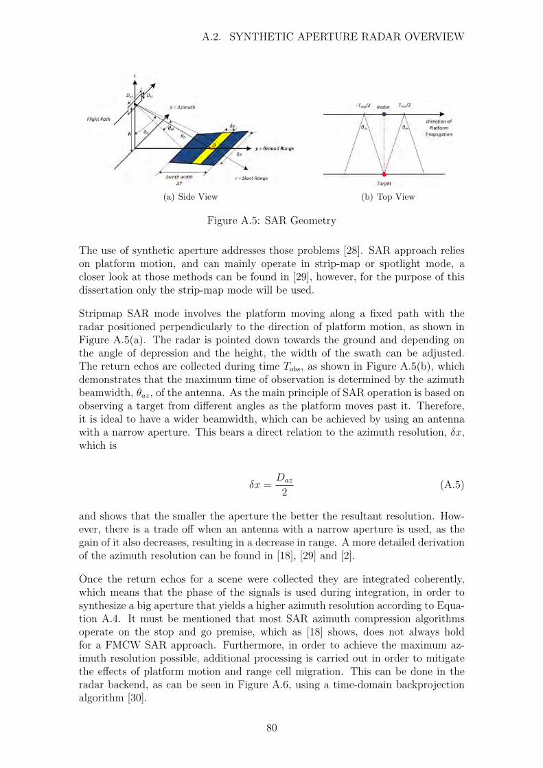
A.2. SYNTHETIC APERTURE RADAR OVERVIEW
(a) Side View (b) Top View
Figure A.5: SAR Geometry
The use of synthetic aperture addresses those problems [28]. SAR approach relieson platform motion, and can mainly operate in strip-map or spotlight mode, acloser look at those methods can be found in [29], however, for the purpose of thisdissertation only the strip-map mode will be used.
Stripmap SAR mode involves the platform moving along a fixed path with theradar positioned perpendicularly to the direction of platform motion, as shown inFigure A.5(a). The radar is pointed down towards the ground and depending onthe angle of depression and the height, the width of the swath can be adjusted.The return echos are collected during time Tobs, as shown in Figure A.5(b), whichdemonstrates that the maximum time of observation is determined by the azimuthbeamwidth, θaz, of the antenna. As the main principle of SAR operation is based onobserving a target from different angles as the platform moves past it. Therefore,it is ideal to have a wider beamwidth, which can be achieved by using an antennawith a narrow aperture. This bears a direct relation to the azimuth resolution, δx,which is
δx =Daz
2(A.5)
and shows that the smaller the aperture the better the resultant resolution. How-ever, there is a trade off when an antenna with a narrow aperture is used, as thegain of it also decreases, resulting in a decrease in range. A more detailed derivationof the azimuth resolution can be found in [18], [29] and [2].
Once the return echos for a scene were collected they are integrated coherently,which means that the phase of the signals is used during integration, in order tosynthesize a big aperture that yields a higher azimuth resolution according to Equa-tion A.4. It must be mentioned that most SAR azimuth compression algorithmsoperate on the stop and go premise, which as [18] shows, does not always holdfor a FMCW SAR approach. Furthermore, in order to achieve the maximum az-imuth resolution possible, additional processing is carried out in order to mitigatethe effects of platform motion and range cell migration. This can be done in theradar backend, as can be seen in Figure A.6, using a time-domain backprojectionalgorithm [30].
80
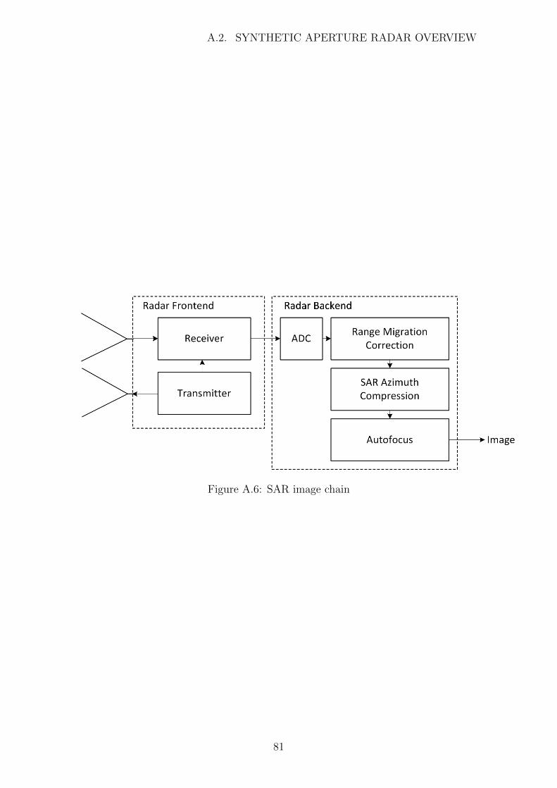
A.2. SYNTHETIC APERTURE RADAR OVERVIEW
Figure A.6: SAR image chain
81

Appendix B
FMCW Radar DesignConsiderations
In its most basic form an FMCW radar consists of a transmitter, antenna andthe receiver. As Figure B.1 suggests each of the three subsystems can be furtherdivided into their respective components. The characteristics of those componentshave a direct effect on the performance of the radar. Hence, in order to be able todesign a system to a particular specification one must understand how the componentparameters effect the performance. This appendix provides the analysis of each ofthe subsystems.
Figure B.1: FMCW imaging radar system diagram
B.1 Transmitter
An FMCW transmitter is a device that produces a signal that has frequency varyingover a set time interval, upon the expiration of which, the cycle repeats. Thisrepetition produces a continuous waveform that is amplified to a power level thatis defined by the desired range of the radar. The higher the signal power, thefurther the theoretical range of detection of the radar. One can distinguish two
82

B.1. TRANSMITTER
processes that occur in the transmitter, which are: waveform generation and signalamplification. However, prior to discussing those two processes, one needs to addressthe parameters that define the waveform.
B.1.1 Waveform Design
During the waveform design phase one must consider a number of parameters thatdefine an L-FMCW waveform. Those parameters are:
• Pulse Repetition Interval (PRI) and Pulse Repetition Frequency (PRF)
• Bandwidth
• Waveform non-linearity
• Chirp rate
• Doppler ambiguity
• Waveform type
PRI and PRF
The waveform can be characterized by the duration of a single cycle, referred toas the Pulse Repetition Interval (PRI), and the number of these cycles over aone second interval, known as the Pulse Repetition Frequency (PRF). The termsPRI and PRF are usually associated with the pulsed radar architecture, however,here they are applied to a continuous wave system. Therefore, the duty cycle ofthe pulse in an FMCW system is said to be set to 100%. Figure B.2(a)and B.2(b),demonstrate these characteristics of the FMCW waveforms using the saw-tooth andthe triangular waveforms as an example and Equation B.1 shows the relationshipbetween the two parameters.
(a) Saw-tooth waveform (b) Triangular waveform
Figure B.2: FMCW waveform design parameters
PRF =1
PRI. (B.1)
83
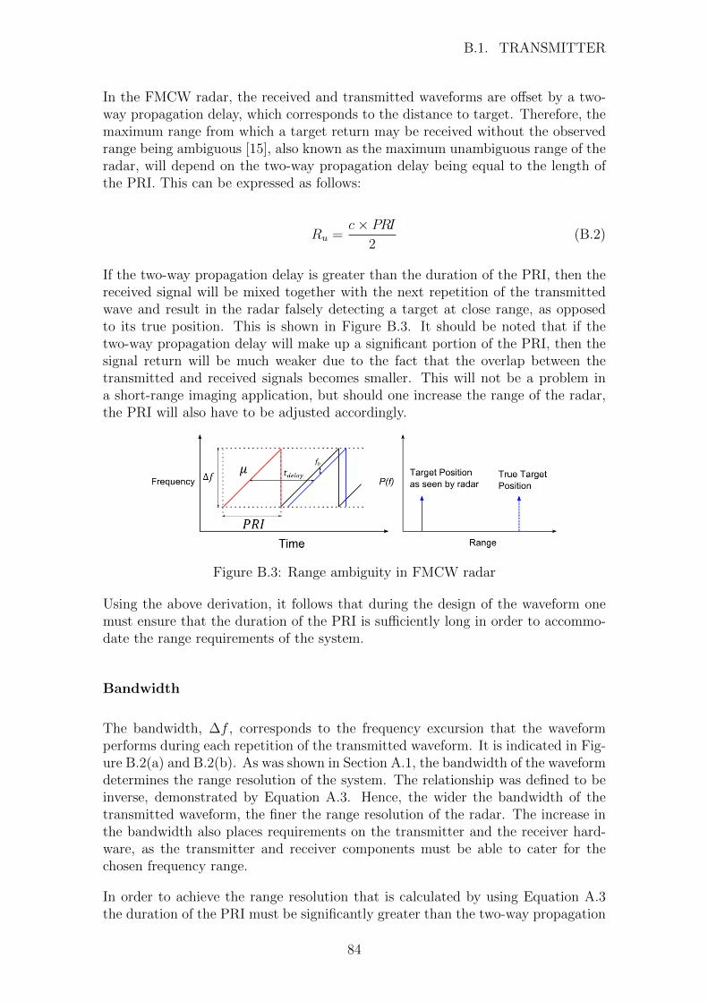
B.1. TRANSMITTER
In the FMCW radar, the received and transmitted waveforms are offset by a two-way propagation delay, which corresponds to the distance to target. Therefore, themaximum range from which a target return may be received without the observedrange being ambiguous [15], also known as the maximum unambiguous range of theradar, will depend on the two-way propagation delay being equal to the length ofthe PRI. This can be expressed as follows:
Ru =c× PRI
2(B.2)
If the two-way propagation delay is greater than the duration of the PRI, then thereceived signal will be mixed together with the next repetition of the transmittedwave and result in the radar falsely detecting a target at close range, as opposedto its true position. This is shown in Figure B.3. It should be noted that if thetwo-way propagation delay will make up a significant portion of the PRI, then thesignal return will be much weaker due to the fact that the overlap between thetransmitted and received signals becomes smaller. This will not be a problem ina short-range imaging application, but should one increase the range of the radar,the PRI will also have to be adjusted accordingly.
Figure B.3: Range ambiguity in FMCW radar
Using the above derivation, it follows that during the design of the waveform onemust ensure that the duration of the PRI is sufficiently long in order to accommo-date the range requirements of the system.
Bandwidth
The bandwidth, ∆f , corresponds to the frequency excursion that the waveformperforms during each repetition of the transmitted waveform. It is indicated in Fig-ure B.2(a) and B.2(b). As was shown in Section A.1, the bandwidth of the waveformdetermines the range resolution of the system. The relationship was defined to beinverse, demonstrated by Equation A.3. Hence, the wider the bandwidth of thetransmitted waveform, the finer the range resolution of the radar. The increase inthe bandwidth also places requirements on the transmitter and the receiver hard-ware, as the transmitter and receiver components must be able to cater for thechosen frequency range.
In order to achieve the range resolution that is calculated by using Equation A.3the duration of the PRI must be significantly greater than the two-way propagation
84

B.1. TRANSMITTER
delay [14]:
PRI � tdelay =2× rc
, (B.3)
where tdelay is the two-way propagation delay and r is the distance to target.
Waveform non-linearity
According to the above definitions one needs to select a suitable duration (PRI) andbandwidth of a single repetition of the waveform in order to determine the maximumunambiguous range and the range resolution. However, this would only apply if thewaveform is perfectly linear. In a practical case the linearity of the waveform woulddeviate. This will depend on the quality of the hardware that is employed.
To account for the expected non-linearity one can use the following relationship [14]:
δf
∆f=δr
Ru
= Waveform non−linearity, (B.4)
where δf is the deviation from the linear waveform. Hence, if the non-linearity factoris exceeded the radar performance that is derived using Equations A.3 and B.2 cannot be expected.
Chirp rate
The chirp rate of the waveform is the ratio of the change in frequency ,∆f , to thechange in time, ∆t, and can be expressed as:
µ =∆f
∆t, (B.5)
where µ is the chirp rate. This essentially represents the slope of the up ramp ofthe waveform. The slope of the up ramp determines the relationship between thebeat frequency signal and the two-way propagation delay. This can be expressedas:
fb = µtdelay (B.6)
In turn, the propagation delay is related to the range to target according to equa-tion A.1. Using this relationship the beat frequency can be related to the range:
fb =2µr
c, (B.7)
85
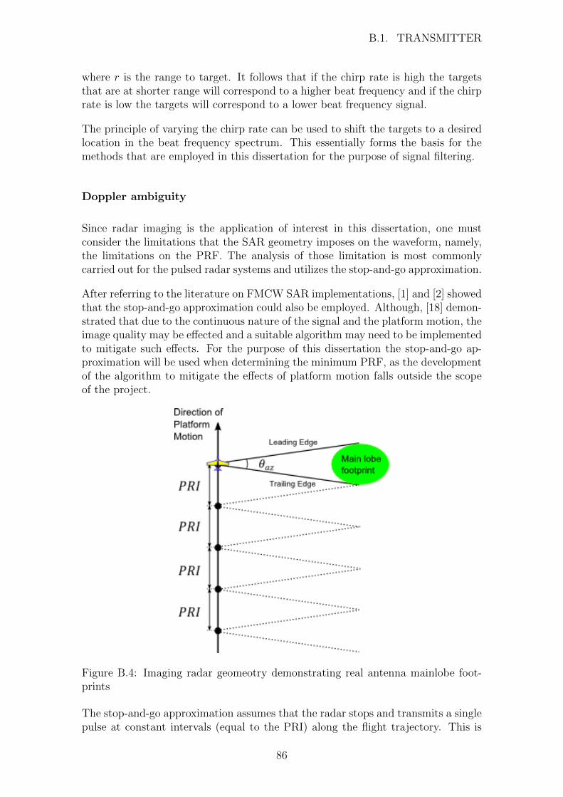
B.1. TRANSMITTER
where r is the range to target. It follows that if the chirp rate is high the targetsthat are at shorter range will correspond to a higher beat frequency and if the chirprate is low the targets will correspond to a lower beat frequency signal.
The principle of varying the chirp rate can be used to shift the targets to a desiredlocation in the beat frequency spectrum. This essentially forms the basis for themethods that are employed in this dissertation for the purpose of signal filtering.
Doppler ambiguity
Since radar imaging is the application of interest in this dissertation, one mustconsider the limitations that the SAR geometry imposes on the waveform, namely,the limitations on the PRF. The analysis of those limitation is most commonlycarried out for the pulsed radar systems and utilizes the stop-and-go approximation.
After referring to the literature on FMCW SAR implementations, [1] and [2] showedthat the stop-and-go approximation could also be employed. Although, [18] demon-strated that due to the continuous nature of the signal and the platform motion, theimage quality may be effected and a suitable algorithm may need to be implementedto mitigate such effects. For the purpose of this dissertation the stop-and-go ap-proximation will be used when determining the minimum PRF, as the developmentof the algorithm to mitigate the effects of platform motion falls outside the scopeof the project.
Figure B.4: Imaging radar geomeotry demonstrating real antenna mainlobe foot-prints
The stop-and-go approximation assumes that the radar stops and transmits a singlepulse at constant intervals (equal to the PRI) along the flight trajectory. This is
86

B.1. TRANSMITTER
shown in Figure B.4. The area that the transmitted signal covers is defined by thedimensions of the real antenna. If one knows the characteristics of the antenna’smain-lobe in azimuth, specifically the difference between the leading and trailingedges of the antenna beam, one can determine the minimum PRF that can be setin order to avoid ambiguity in the azimuth direction. This ambiguity is known asthe Doppler ambiguity.
Figure B.5: In order to avoid Doppler ambiguities the PRF must exceed the dif-ference between the Doppler shifts at the leading and trailing edges of the realantenna’s mainlobe [15]
The leading and trailing edges of the main-lobe of the real antenna are demonstratedin Figure B.4. The case where a suitable PRF was chosen in order to avoid overlapof the main-lobes is shown in Figure B.5. If the antenna main-lobe footprints willoverlap, Doppler ambiguity will occur. Hence, the minimum PRF that can bechosen must abide by the following expression:
PRFmin = fdL − fdT , (B.8)
where fdL and fdT are the Doppler frequencies at the main-lobe’s leading and trailingedges [15].
In a case where the real antenna has a narrow azimuth beamwidth, the minimumPRF can be calculated by using the following expression:
PRFmin =2vθNNaλ
, (B.9)
where v is the velocity of the radar, θNNa is the null-to-null azimuth beamwidthof the real antenna in radians and λ is the wavelength of the transmitted signal.Equation B.9 makes the assumption that the radar is perpendicular to the directionof platform motion.
87
B.1. TRANSMITTER
Waveform type
The two types of waveforms that have been used in the above design discussion arethe saw-tooth and the triangular modulated waveforms. They are widely used inpractice, however they are not the only modulations that can be used.
The saw-tooth waveform has an advantage over the triangular waveform, in thatone can achieve a higher PRF. This is apparent if one compares Figure B.2(a) andFigure B.2(b), the chirp rates are the same for both cases, but since the triangularwaveform also has a down ramp of the same duration the PRI is effectively doubled.
As was mentioned in Section A.1, the down ramp of the triangular waveform allowsone to determine the Doppler frequency shift, as well as the range information froma single sweep. In addition to that an advantage of the triangular waveform is thatthe return from a high frequency to the lower frequency occurs smoothly due to thefact that there is a up ramp and down ramp. The saw-tooth waveform modulationtechnique might result in an undershoot between repetition as the change from thehigh frequency to low frequency occurs in a very short period of time.
B.1.2 Waveform Generation
The waveform generator is the part of the transmitter that is responsible for generat-ing the frequency modulated continuous waveform. The waveform that is producedalso has to be centred at the desired carrier frequency. Two methods of waveformgeneration have been encountered in the literature:
• Direct Digital Synthesizer (DDS)
• Voltage Controlled Oscillator (VCO) driven by a tuning voltage
Direct Digital Synthesizer (DDS) approach
The DDS approach entails generating a frequency modulated signal at basebandand then stepping up the frequency to the desired carrier frequency. This approachwas utilizes in Brigham Young University’s (BYU) µSAR [3] and microASAR [4]systems.
The DDS generates a discrete-time signal, which it then converts to its analog formby using the Digital-to-analog converter (DAC). The output frequency of the DDSdepends on the reference clock of the system and the binary number or tuningword [7]. Basic components of a DDS device can be seen in Figure B.6 and theyare the phase accumulator, phase-to-amplitude converter and the DAC.
The tuning word is typically stored in a frequency register and can be seen at theinput of the phase accumulator. The phase accumulator computes a phase addressfor the look-up table and the corresponding phase is converted to an amplitude
88

B.1. TRANSMITTER
Figure B.6: Components of a direct digital synthesizer [7]
in the phase-to-amplitude converter. This amplitude is a digital value, which isthen converted to an analog signal using the DAC. The rate at which the phaseaccumulator steps through the phase look-up table determines the frequency ofthe output signal. If a slow rate is chosen to step through the look-up table, asinusoidal wave at a low frequency is produced. In a case where a fast rate is used,a higher frequency sinusoidal wave is produced. Finally, if the rate at which thephase accumulator steps through the look-up table is varied, a frequency modulatedsignal can be produced.
The advantage of the DDS approach lies in the fact that they operate at low power,can provide fast switching between output frequencies, fine frequency resolutionand are available at a low cost [31]. Furthermore, the output waveform can bereprogrammed and the properties of the output waveform can be easily changed.This was employed in BYU microASAR, where the PRF of the output waveformwas variable in order to account for the altitude of the platform.
Possible disadvantages of the DDS approach include the fact that since a DAC isused to produce the analog output, Nyquist images are also produced and therefor areconstruction lowpass filter needs to be added to the system. Another disadvantageis the fact that the output frequency is limited to baseband and needs to be steppedup to the desired carrier frequency.
Voltage Controlled Oscillator (VCO) approach
Voltage Controlled Oscillator (VCO) outputs a frequency in linear proportion toits input control voltage. This method of producing the modulated waveform wasused in the rail SAR setup in [1], TU Delft’s demonstrator system [18] and theMassachusetts Institute of Technology (MIT) Independent Activity Period (IAP)radar setup [11].
The main issue with this approach is the fact that the VCOs tend to have a non-linear response to a linear tuning voltage. This can be illustrated by Figure B.7(a),where a linear tuning voltage would result in the demonstrated non-linear responseof the VCO. To solve this problem, a tuning voltage profile that is shown in Fig-ure B.7(b) will be required to compensate for the VCO non-linearity.
The linearity of the output waveform determines the performance of the radar, aswas shown in Section B.1.1, therefore the above mentioned voltage profile that com-pensates the non-linearity is required. This can be done using a feedback system,
89

B.1. TRANSMITTER
where the output of the VCO is compared to the expected frequency as determinedby the tuning voltage.
(a) VCO response (b) Compensation tuning volt-age
Figure B.7: An exaggerated non-linear response of the VCO with the correspondingtuning voltage that is required for compensations [1]
For example, if a DAC is used to produce a tuning voltage, an output of the VCO canbe fed back to the micro-controller or the computer that is responsible for producingthe waveform and determine the disparity between the expected and the actualoutput of the VCO. After that the tuning voltage profile is changed to account forthe non-linearities and fixed to that tuning profile for all the subsequent waveforms,as was done in [1]. Alternatively, the algorithm can carry out the adjustment on apulse to pulse basis, continually improving the profile of the tuning voltage, as wasdone in [18].
Recently, complete systems on a chip that in conjunction with a VCO can carry outhigh frequency ramp generation started to emerge. A PLL that can be frequencymodulated by varying the feedback signal from the VCO is one of them. Thisprovides an alternative to the above mentioned approach, where the non-linearityof the VCO output is compensated using a predetermined algorithm that is executedon the micro-controller or any other processing unit.
The advantage of the VCO approach lies in the fact that a VCO that operates inthe frequency range of interest can be chosen and the waveform can be producedat the carrier frequency, with out the need to step it up to the carrier frequency asis required when using a DDS.
B.1.3 Signal Amplification
The methods of generation that were explained in the previous section produce amodulated waveform at a relatively low power level. The Friis transmission equa-tion, which is used to estimate the performance of radio communication and broad-cast stations [32], shows that the power of the transmitted signal influences theexpected range of signal propagation. The relationship is expressed as follows:
90

B.1. TRANSMITTER
Prx = Ptx
(λ
4πR
)2
GtxGrx, (B.10)
where, Prx is the power received at the receiver antenna and Ptx is the powertransmitted. Gtx and Grx are the transmitter and receiver antenna gains and R isthe range between the antennas.
The relationship between transmitted and received power demonstrates that if thetransmitted power is increased, so will the power at the receiver antenna. However,if the range between antennas increases, the power at the receiver decreases.
Despite the fact that in the case of radar, the range of interest is typically double therange in the above equation, as the signal needs to travel to the target and returnback to the radar. The relationship between transmitter and receiver power levelsis directly proportional, as in Equation B.10. Therefore, given a specified rangethat the radar must operate in, one needs to ensure that the transmitter power issufficiently high in order to receive a satisfactory power level at the receiver antenna.
To accomplish this the output of the waveform generator is fed into a power ampli-fier, which can be characterized by the following parameters:
• Operating frequency range
• Gain and gain flatness
• Output power at 1 dB compression point
• Output third-order intercept point (OIP3)
Operating frequency range
When choosing an amplifier for a particular application one needs to ensure that itis able to operate in the frequency range of interest. Given the imaging applicationof the radar, the bandwidth of the transmitted signal is desired to be wide dueto the fact that it is responsible for determining range resolution. Hence, oneneeds to ensure that the amplifier of choice can operate predictably across the widefrequency range. This means that the parameters, such as gain, gain flatness andoutput third-order intercept points should be stable across the desired range.
Amplifier gain and gain flatness
The gain of the amplifier is the ratio of output power to the input power, specifiedin small-signal linear gain region [8]. It is measured in decibels (dB) and is relativelyconstant across the frequency range of the amplifier. The variance in the gain ofthe amplifier across the frequency range of operation is characterized by the gainflatness parameter.
91
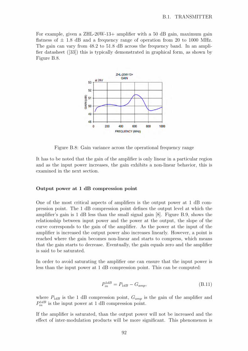
B.1. TRANSMITTER
For example, given a ZHL-20W-13+ amplifier with a 50 dB gain, maximum gainflatness of ± 1.8 dB and a frequency range of operation from 20 to 1000 MHz.The gain can vary from 48.2 to 51.8 dB across the frequency band. In an ampli-fier datasheet ([33]) this is typically demonstrated in graphical form, as shown byFigure B.8.
Figure B.8: Gain variance across the operational frequency range
It has to be noted that the gain of the amplifier is only linear in a particular regionand as the input power increases, the gain exhibits a non-linear behavior, this isexamined in the next section.
Output power at 1 dB compression point
One of the most critical aspects of amplifiers is the output power at 1 dB com-pression point. The 1 dB compression point defines the output level at which theamplifier’s gain is 1 dB less than the small signal gain [8]. Figure B.9, shows therelationship between input power and the power at the output, the slope of thecurve corresponds to the gain of the amplifier. As the power at the input of theamplifier is increased the output power also increases linearly. However, a point isreached where the gain becomes non-linear and starts to compress, which meansthat the gain starts to decrease. Eventually, the gain equals zero and the amplifieris said to be saturated.
In order to avoid saturating the amplifier one can ensure that the input power isless than the input power at 1 dB compression point. This can be computed:
P 1dBin = P1dB −Gamp, (B.11)
where P1dB is the 1 dB compression point, Gamp is the gain of the amplifier andP 1dBin is the input power at 1 dB compression point.
If the amplifier is saturated, than the output power will not be increased and theeffect of inter-modulation products will be more significant. This phenomenon is
92

B.1. TRANSMITTER
Figure B.9: 1 dB compression point of a typical amplifier [8]
addressed in the following section.
Output third-order intercept point
The non-linear behavior of a amplifier results in the formation of output harmon-ics [34]. The harmonic responses are undesired and need to be removed from theoutput signal. Given single frequency input at frequency f1,the harmonics will beformed at n× f1, where n is the order of the harmonic. Figure B.10 demonstratesthe presence of harmonics at a output of the amplifier that has an input signallocated at 2.4 GHz. It can be seen that given a high frequency input signal, theharmonic responses are located relatively far from the original signal. Hence, a filtercan be used to filter the unwanted harmonics out.
Figure B.10: nFirst order harmonics of a 2.4 GHz signal at the output of the amplifier
In the case where there are two signals at the input of the amplifier located atfrequencies f1 and f2 within the operational range of the amplifier, the harmonicswill appear at m× f1 +n× f2, with the order of the harmonics equal to the sum of
93
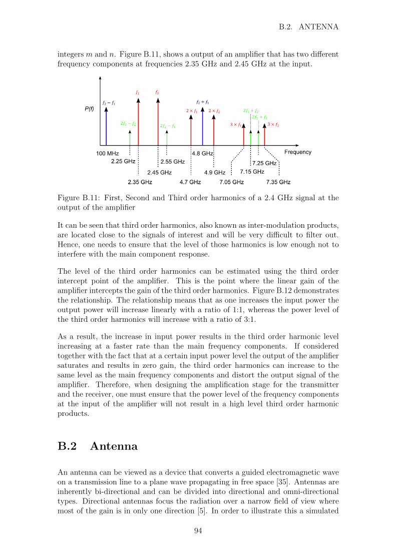
B.2. ANTENNA
integers m and n. Figure B.11, shows a output of an amplifier that has two differentfrequency components at frequencies 2.35 GHz and 2.45 GHz at the input.
Figure B.11: First, Second and Third order harmonics of a 2.4 GHz signal at theoutput of the amplifier
It can be seen that third order harmonics, also known as inter-modulation products,are located close to the signals of interest and will be very difficult to filter out.Hence, one needs to ensure that the level of those harmonics is low enough not tointerfere with the main component response.
The level of the third order harmonics can be estimated using the third orderintercept point of the amplifier. This is the point where the linear gain of theamplifier intercepts the gain of the third order harmonics. Figure B.12 demonstratesthe relationship. The relationship means that as one increases the input power theoutput power will increase linearly with a ratio of 1:1, whereas the power level ofthe third order harmonics will increase with a ratio of 3:1.
As a result, the increase in input power results in the third order harmonic levelincreasing at a faster rate than the main frequency components. If consideredtogether with the fact that at a certain input power level the output of the amplifiersaturates and results in zero gain, the third order harmonics can increase to thesame level as the main frequency components and distort the output signal of theamplifier. Therefore, when designing the amplification stage for the transmitterand the receiver, one must ensure that the power level of the frequency componentsat the input of the amplifier will not result in a high level third order harmonicproducts.
B.2 Antenna
An antenna can be viewed as a device that converts a guided electromagnetic waveon a transmission line to a plane wave propagating in free space [35]. Antennas areinherently bi-directional and can be divided into directional and omni-directionaltypes. Directional antennas focus the radiation over a narrow field of view wheremost of the gain is in only one direction [5]. In order to illustrate this a simulated
94

B.2. ANTENNA
Figure B.12: Linear gain of the amplifier vs. the gain of the third order intermod-ulation products [8]
pattern of a main beam can be seen in Figure B.14. This figure demonstrates the3-dimensional antenna pattern for a horn antenna and shows that most of the poweris focused in the direction of the z-axis.
In contrast to the directional antennas, omni-directional antennas radiate equallyin all directions. An example of omni-directional antenna is the dipole antenna.
For the purpose of this dissertation only the directional type of antennas will beanalyzed, as that is the type of antenna that is required for an imaging radarapplication. Furthermore, the details of electromagnetic theory will be omitted,instead the properties that directly relate to the operational aspects of the antennaswill be examined, namely:
• Frequency of Operation
• Half-Power Beamwidth
• Gain
• Aperture Efficiency
• Bi-static radar and Imaging Application Design Considerations
B.2.1 Frequency of Operation
As the signal that is produced at the transmitter is centered at a particular carrierfrequency, the antenna must be designed so that it is capable to radiate efficiently
95

B.2. ANTENNA
Figure B.13: 3D antenna pattern of a standard gain horn [5]
across the required signal bandwidth. The antenna bandwidth is the region wherethe key antenna parameters are within a desired range [26]. A parameter that is ofparticular interest, is the return loss, which is typically required to be below -10 dB.The -10 dB return loss implies that the power at that point is 90% of the maximumpower of the main beam [26].
The bandwidth of the antenna can be represented by a percentage, where the upperand lower cut-off frequencies correspond to a region where the return loss is -10 dB.The expression for the antenna bandwidth is as follows:
BWant =fU − fLfo
× 100[%], (B.12)
where BWant is the antenna bandwidth, fU and fL is the upper and lower cut-offfrequencies and fo is computed as:
fo =fU − fL
2. (B.13)
B.2.2 Half-Power Beamwidth
In order to define the half-power beamwidth or 3-dB beamwidth, the antenna pat-tern must be examined. This is shown in Figure B.14, where a 2-dimensionalrepresentation of a typical antenna pattern is demonstrated. The antenna patternconsists of a main beam (main lobe) and additional minor lobes (side lobes), thehalf power beamwidth of the antenna is defined as the angle in degrees between the
96

B.2. ANTENNA
points on the left and right side of the main beam where the transmitted power isdecreased by half of its peak value.
Figure B.14: Radiation pattern of a directional antenna indicating the left and righthalf-power points used to calculate the antenna beamwidth [36]
If one uses the decibel scale, the half-power beamwidth is called the 3-dB beamwidth,as a 3 decibel decrease in power level corresponds to decrease in power by a factorof 2.
Therefore, if the antenna is said to have a 3-dB beamwidth of 8 degrees, the poweris reduced to half its maximum value 4 degrees to the left and right of the centreof the main lobe.
B.2.3 Gain
The gain of an antenna is defined as 4π times the ratio of maximum radiationintensity to the net input power into the antenna [26]. This can be expressed as:
G =4πUmaxPmax
, (B.14)
where Umax is the maximum radiation intensity and Pmax is the antenna inputpower. A usefull approximation of this formula is found in [32] and can be usedwhen the half-power beamwidth of the directional antenna are known:
G ' 10 · log(ρ
4π
ΘHΘE
), (B.15)
97
B.3. RECEIVER
where ρ is the antenna efficiency, ΘH and ΘE are the orthogonal half-power beamwidthscorresponding to the magnetic and electric field planes [5].
Antenna efficiency is usually greater than 90% for the antennas that have a goodimpedance match. A good impedance match is responsible for efficient power trans-fer as is shown in [37], which in turn effect the antenna efficiency. Other factors, suchas polarization mismatch with the receiver antenna can also effect the efficiency.
B.2.4 Aperture Efficiency
An antenna aperture largely determines the direction of propagation of the electro-magnetic radiation in the antenna and is responsible for intercepting the incomingelectromagnetic radiation when operating as a receiver. The effective cross-sectionof the antenna can be used to determine the antenna performance.
Aperture efficiency, which is the effective cross-section area of the antenna, is di-rectly proportional to the gain of the antenna, therefore a higher gain will yield alarger effective aperture. The relationship between the two parameters is as follows:
Aeff =Gλ2
4π, (B.16)
where G is measured in linear units and not decibels. This relationship was usedin Section A.2 to explain the reason behind not employing an antenna with a smallaperture to obtain a higher azimuth resolution in a SAR system, as the gain willalso decrease and reduce the maximum range of the system.
B.3 Receiver
The receiver of a homodyne (direct conversion) type consists of a Low Noise Am-plifier, a frequency mixer, an IF amplifier and a filter stage prior to the ADC thatconverts the analogue signal data into the digital domain for processing. The pa-rameters that one should consider when specifying the receiver are:
• Noise Figure
• Receiver Sensitivity
• Dynamic Range
• ADC Sampling Frequency
• Storage Rate
98

B.3. RECEIVER
B.3.1 Noise Figure
Noise figure is a measure of how much a given two-port device, such as an amplifier,degrades the signal-to-noise (SNR) of a given input signal. Sources of noise includethermal noise, shot noise and other effects due to the physics of various types oftransistors, all of which are combined into the noise factor (F ) [5].
The noise factor can be defined as the ratio between the SNR of the input signal(Si/Ni)to the SNR of the output signal (So/No):
F =Si/Ni
So/No
. (B.17)
The noise figure, which is the parameter that is typically used to characterize thenoise associated with the LNA is equal to:
NF = 10× log10F, (B.18)
where NF is the noise figure in decibels [5].
To compute the noise figure for the receiver of the radar, one needs to considerthe contributions of all the components in the chain and derive the cascaded noisefigure.
The first element of the receiver is the LNA, which is designed to have a low noisefigure. This is crucial, as it contributes the most to the overall noise figure of thereceiver due to the fact that it is the first element of the receiver chain.
Other components in the receiver, apart from the IF amplifier, do not have a noisefigure specification, instead their insertion loss parameter. As a result a receiverthat consists of n elements will have the following cascaded noise figure [5]
NFsys = 10×(F1 +
F2 − 1
G1
+F3 − 1
G1G2
+F4 − 1
G1G2G3
...Fn − 1
G1G2G3...Gn−1
), (B.19)
where Fn is the noise factor and Gn is the gain of each stage of a receiver chain.
B.3.2 Receiver Sensitivity
Receiver sensitivity defines the weakest signal that can be detected by the radarsetup. This is also known as the Minimum Detectable Signal (MDS) and is measuredin dBm [13] [5]. The noise that is associated with the radar receiver essentially setsthe limit on the MDS, as is shown by Equation B.20.
99
B.3. RECEIVER
MDS = 10log10
(kT0
1mW
)+NFsys + 10log(BWrec) + SNRout, (B.20)
where k is the Boltzmann’s constant (1.38 × 10⁻²³ joules/Kelvin), BWrec is thereceiver bandwidth (Hz) and SNRout is the minimum required SNR for detection.
B.3.3 Dynamic Range
The dynamic range of the receiver is defined as the ratio of the maximum signalthat can be handled to the smallest signal capable of being detected. The smallestsignal is the MDS as determined by the receiver noise and the maximum signalis that which causes a specified degree of intermodulation or a specified deviationfrom linearity of the output-vs.-input curve [13].
As was mentioned in Section B.1.3, an amplifier becomes saturated when the inputpower is higher than the difference between power at 1 dB compression and theamplifier gain (Equation B.11). When the amplifier is saturated the third-orderintermodulation products can severely effect the signal at the output. Hence, theupper limited of the dynamic range can be said to be the input power level that isfound just before the input amplifiers gain starts to compress.
Automatic gain control (AGC) can be used in a superheterodyne receiver to decreasethe gain when strong signals can cause overload or distortion, although there maybe trade-offs for the SNR performance [37].
B.3.4 ADC Sampling Frequency and Dynamic Range
The sampling frequency of the ADC essentially determines the frequency band thatcan be processed by the receiver. For example, if the sampling rate of the systemis 125 Megasamples per second (Msps), then the highest frequency of a real signalthat can be sampled is 62.5 MHz, according to the Nyquist sampling theorem.
Furthermore, the dynamic range of the ADC, which is defined to be the ratio ofthe rms value of the full scale to the rms noise. It indicates the range of signalamplitude that the ADC can resolve and can be calculated by using the followingequation [38]:
DR = 6.021N + 1.763, (B.21)
where N is the number of bits that the ADC uses to store the digitized analogsignal.
100
B.3. RECEIVER
B.3.5 System Storage Rate
If a radar system that is to be mounted on a small airborne platform is designedto operate on the “turn on and forget” basis, where the radar is switched on andthe system records the data until the storage space is filled, the storage rate of thesystem can place a limitation on the other design parameters. This was the case inmicroASAR [4], where due to the high PRF, the amount of data that needed to bestored required a storage rate of 48 Mbytes/s. The hardware that was available tothe designers was only capable of a storage rate of 5 MBytes/s. Hence, pre-summingof data that lead to a decrease in azimuth resolution had to be done.
One can calculate the required storage rate by considering the frequency range atthe input to the ADC and doubling it in order to comply with the Nyquist samplingtheorem, this will correspond to the number of samples per second that need to bestored.
Sample Rate = Maximum Frequency × 2 (B.22)
Then knowing that number of bits that the ADC uses to store the data, one cancalculate the data rate in bits per second.
Data Rate = Sample Rate× Bits per Sample (B.23)
This corresponds to the storage rate that the system will require to store the in-coming data.
101