design and implementation of a grid connected solar micro...
TRANSCRIPT

Design and Implementation of a Grid Connected Solar Micro-inverter
Prepared for: ECE 4600
Prepared by: Raveen Gunarath
Luo Liu Sarin Rajapakse Ella Thomson
Advisor:
Dr. Carl Ho
Department of Electrical and Computer Engineering University of Manitoba
Winnipeg, Manitoba, Canada
March 2017
© Raveen Gunarath, Luo Liu, Sarin Rajapakse, Ella Thomson

Abstract The purpose of this project was to design a grid connected solar micro inverter. Solar
microinverters convert the power from a photovoltaic panel to power that can be injected into the
grid. In this project, the solar micro inverter was designed using a DC-DC converter stage and a
DC-AC inverter stage. Maximum power point tracking was used to maximize the power drawn
from the photovoltaic panel in the DC-DC converter stage. Controllers were also designed for the
DC-AC inverter stage. A simulation of the system was completed on Plexim. The simulation
realized all design specifications. These specifications were a 200 V DC link voltage, a
output voltage and maximum power point tracking. A prototyping stage was20 V rms %1 ± 5
completed using perf board fabricated circuits. This stage was completed to validate the design of
the physical system. The final project deliverables were a fully populated PCB and a complete set
of microcontroller code. The DC link voltage was 200 Volts. The output AC voltage was 116 V
rms, which was within the specification of . The efficiency of the DC-DC20 V rms %1 ± 5
converter stage was 91%. The efficiency of the DC-AC inverter stage was 93%. The overall
efficiency was 85%, which met the specification of efficiency greater than 80%.

Acknowledgements We would like to thank our supervisor, Professor Carl Ho, for his guidance and assistance
with the project. We would also like to thank several graduate students in the power systems
group at the University of Manitoba, including Mandip Pokharel, Dong Li, Isuru Jayawardana,
King Man Siu and Yang Zhou. We would also like to thank Professor Card for his technical
assistance with the project. We would like to thank Erwin Dirks for allowing us to borrow several
power circuit components. We also thank Glen Kolansky and all other lab technicians in ECE for
their assistance in providing us with the required circuit components. Additionally, we would like
to thank VITEC for providing us with the flyback transformer.

Contribution Page The work was evenly shared amongst all team members. The project was divided into 5
design stages. Each design stage was assigned one primary lead and one secondary lead, to
provide redundancy. The design leads were responsible for dividing work amongst themselves
and assigning tasks to other team members. Each team member acted as primary lead for one
design stage, and secondary lead for another design stage. The final implementation and testing
stage required the expertise and background knowledge of all team members. Therefore, the work
for this stage was divided equally amongst the team. The design stages are bolded. Individual
tasks are specified under each design stage. The work completed by each team member is
summarized below.
Task Raveen Gunarath
Luo Liu Sarin Rajapakse
Ella Thomson
Topology X
Simulation O X O O
Prototyping O O O X
PCB Design X O
Control Development
O X O
Implementation O O O O
Legend X = Team Lead O = Contributed

Table of Contents Abstract…………………………………………………………………………………….i
Acknowledgements………………………………………………………………………..ii
Contribution Page………………………………………………………………………...iii
Table of Contents………………………………………………………………………....iv
List of Figures…………………………………………………………………………….vi
List of Tables……………………………………………………………………………viii
Nomenclature…………………………………………………………………………….ix
1.1 Project Purpose………………………………………………………………………………...1
1.2 Overview of Document………………………………………………………………………...1
1.3 Background…………………………………………………………………………………….1
1.3.1 Overview of Solar Energy in Canada
1.3.2 Advantages and Disadvantages of Solar Energy
1.3.3 Microinverters versus Inverters
1.3.4 Function of Solar Microinverters
1.3.5 Extracting MAximum Power from a Solar Microinverter
2.1 Design Specifications…………………………………………………………………………..5
2.2 Design Methodology and Staging……………………………………………………………...5
3.1 DC-DC Converter……………………………………………………………………………...7
3.2 DC-AC Inverter………………………………………………………………………………...9
3.3 Filter Design…………………………………………………………………………………..11
4.1 Design and Validation on Plecs …………………………………………………...…...…….12
4.2 Simulation Design Process…………………………………………………………………....14
4.3 Maximum Power Point Tracking Results- Simulation……………………………………….14
4.4 DC Link Voltage Results- Simulation ……………………………………...……...………...15
4.5 Output of DC-AC Inverter Stage Simulation………………………………………………....16
4.6 Summary of Simulation Results……………………………………………………………...17
5.1 Physical Testing of the DC-DC Converter Stage…………………………………………….18
5.2 Physical Testing of DC-AC Inverter Stage…………………………………………………...20
5.3 Design of Step Down Circuits………………………………………………………………..22
5.4 Summary of Physical Builds………………………………………………………………….24
6.1 Trace Width Design ……………………………………………………………......………...30
6.2 Selection of Components Style and Placement of Components……………………………...30
6.3 Selection of Number of Boards……………………………………………………………….30

6.4 Complete PCB………………………………………………………………………………...31
7.1 Maximum Power Point Tracking……………………………………………………………..33
7.2 DC-AC Current Control (inner loop)........................................................................................34
7.3 Deadband Circuit……………………………………………………………………………..35
7.4 DC Link Voltage Control (outer loop)......................................................................................36
8.1 DC-DC Converter with Maximum Power Point Tracking ……………...……………...…....38
8.2 DC-AC Converter with Open Loop Controls………………………………………………...41
8.3 DC-AC Converter with Closed Loop Current Control……………………………………….45
8.4 DC Link Voltage Regulation and Grid Connection…………………………………………..46
9.1 Summary of Design Specifications…………………………………………………………...48
9.2 Added Value Features………………………………………………………………………...49
9.3 Future Work………………………………………………………………………...,..............49
9.4 Conclusions ……………………………………………………………...…………………...49
Bibliography……………………………………………………………………………..50

List of Figures
Figure 1-1: Parallel Connection of Micro-Inverters……………………………………...………..2
Figure 1-2: Simple circuit model for a photovoltaic cell………………………………...……..….3
Figure 1-3: IV curve for a solar panel……………………………………………………....……...4
Figure 3-1: Block diagram of grid connected solar micro-inverter………………………...……...7
Figure 3-2. Fly-back DC-DC converter………………………………………………………...….7
Figure 3-3: Flyback DC to DC converter operation…………………………………………...…..8
Figure 3-4: H bridge full inverter………………………………………………………………......9
Figure 3-5: Gate driver circuit………………………………………………………………...….10
Figure 3-6. Full bridge IGBT Inverter………………………………………………………...….10
Figure 4-1: Complete simulation schematic………………………………………………….......13
Figure 4-2: Output of maximum power point tracking ……………………………………...…..15
Figure 4-3: DC link voltage in simulation time in seconds ………………………………….......16
Figure 4-4: Current, voltage and power outputs of the DC-AC inverter stage……………....…...16
Figure 5-1: DC-DC converter stage physical testing schematic……………………………....….18
Figure 5-2: Setup for DC-DC converter testing …………………………………………....…....19
Figure 5-3: 15 Volts at the output of the DC-DC converter……………………...…………........19
Figure 5-4: MOSFET switching signals……………………………………………………...…..20
Figure 5-5: Setup for testing DC-AC inverter stage……………………………………………...20
Figure 5-6: Output of DC-AC converter using signal generator and NOT Gate……………........21
Figure 5-7: Output of DC-AC converter with microcontroller programming……………....…....22
Figure 5-8: DC voltage step down circuits…………………………………………………....….23
Figure 5-9: AC step down circuit………………………………………………………….……...23
Figure 5-10: Output of AC control circuits………………………………………………….........24
Figure 6-1: DC-DC schematic for PCB……………………………………………………....…..25
Figure 6-2: DC-AC PCB schematic……………………………………………………....……....26
Figure 6-3: DC step down circuit…………………………………………………………....…....27
Figure 6-4: AC step down and shifter circuit……………………………………………....……..27
Figure 6-5: Output connector PCB schematic………………………………………………...….28
Figure 6-6: Complete PCB schematic………………………………………………………....….29
Figure 6-7: Completed PCB Design………………………………………………………....…...31
Figure 6-8: Fully populated PCB………………………………………………………….……...31

Figure 7-1: DC-DC converter close loop code …………………………………………....……..34
Figure 7-2: MPPT control block………………………………………………………....……….34
Figure 7-3: Flyback gate controller block………………………………………………....……...34
Figure 7-4: Hysteresis control loop……………………………………………………....……….35
Figure 7-5: Deadband circuit……………………………………………………………………..35
Figure 7-6. Output of dead time circuit yellow is V1 and the green is V2…………………....….36
Figure 7-7: Outer loop DC link voltage controller…………………………………………...…..37
Figure 8-1: Block diagram for DC-DC converter test with MPPT……………………………....38
Figure 8-2: Setup for DC-DC converter test with maximum power point tracking……………...39
Figure 8-3: Maximum Power Point tracking at varying irradiance levels…………………...…..40
Figure 8-4: Simulated PV curves at varying inductance levels……………………………...…...40
Figure 8-5: DC-AC converter test with open loop controls...........................................................42
Figure 8-6: 330 V peak to peak output voltage with open loop controls…………………...…....43
Figure 8-7: Output current with open loop controls………………………………………...…....43
Figure 8-8: Input voltage and current………………………………………………………...…..44
Figure 8-9: Output voltage and current for open loop DC-AC testing……………………....…...44
Figure 8-10: AC current control testing setup…………………………………………………....45
Figure 8-11: Output for testing grid current control……………………………………………...46
Figure 8-12: Setup for testing DC link voltage control…………………………………………..47
Figure 8-13: Output of DC link voltage testing…………………………………………………..47

List of Tables
Table 2-1: Design Specifications………………………………………………………………..…5
Table 4-1: DC- DC Converter Parameter Values ………………………………………………..12
Table 4-2: DC-AC Inverter Parameter Values ……………………………………………….…..14
Table 7-1: PI Parameters for MPPT ………………………………………………………….…..33
Table 7-2: Parameters for PI controller in outer loop DC link voltage control ………...……......37
Table 8-1: PI parameters in Simulink for maximum power point tracking………………….…...39
Table 8-2: Differences in measured and simulated maximum power…………………………….41
Table 8-3: Output filter parameters………………………………………………………….…...42
Table 9-1: Final design results……………………………………………………...…………….46

Nomenclature Page
Symbol Description Use
A Amperes Unit for current
V Volts Unit for voltage
rms root mean square value Used to describe AC voltages and currents
W Watts Unit for power
p-p peak to peak Used to describe AC voltages and currents
MPPT Maximum Power Point Tracking
A method used to find the maximum power point of a PV panel output voltage and current
D Duty Cycle
The fraction of one period in which a signal or system is active
PWM Pulse Width Modulation A modulation technique to control the duty cycle of a square wave
AC Alternating Current An electric current that reverses its direction with certain frequency
DC Direct Current An electric current that has fixed direction
PCB Printed Circuit Board A board that electrically connects components
PV Photovoltaic A method for generating electric power by using solar energy

Chapter 1- Introduction This section includes the project purpose, and an overview of the document. Background
information about solar energy and microinverters is also discussed.
1.1 Project Purpose
The purpose of this project was to design and implement a grid connected solar
micro-inverter. The project deliverables were divided into three subsections. The first deliverable
was a simulation, completed using the Plecs design and simulation tool. The simulation included
both the DC-DC converter , DC-AC converter and also the closed loop controls. The second
deliverable was physical builds of the DC-DC and DC-AC converters, to verify the circuit
topology and then PCB design and for the full power circuits. The third deliverable was
microcontroller programming for closed loop control and maximum power point tracking. The
input to the converter was a solar panel, modeled using a lab volt PV simulator. The output of the
converter was connected to the grid (120 Vrms and 60 Hz). The purpose of the project was to
design an inverter with an overall efficiency of over 80%.
1.2 Overview of Document
This document includes all major design goals, methodology and results for the design
and implementation of a solar micro-inverter. Background information related to solar panels is
presented. The design methodology and specifications are then stated. The simulation design
process and results are discussed, followed by the physical build results, the design process for
the PCB and the microcontroller programming methodology. The results of the subsystem
integration are presented, and the overall success of the project is evaluated, as it relates to the
design goals.
1.3 Background
This section includes background information regarding solar energy, micro-inverters,
and the purpose and implementation of maximum power point tracking.
1.3.1 Overview of Solar Energy in Canada
The purpose of this project was to design and implement a single-phase grid connected
solar micro-inverter. The design of a solar micro-inverter is relevant as renewable energy is
becoming more popular due to an interest in replacing fossil fuels and in slowing the progression
1

of climate change. As of 2013, over 63% of Canada’s energy usage was considered renewable
[1]. Hydro power alone accounts for approximately 60% of energy usage [1]. Solar energy
currently comprises a small portion of energy production in Canada. However, solar energy usage
in Canada has grown by 13.8% from 2004-2014 [2].
1.3.2 Advantages and Disadvantages of Solar Energy
Solar panels have several advantages. Solar energy is fully renewable. Additionally, the
panels require little maintenance, in comparison to other forms of renewable energy such as wind
energy, or hydro power [3].
One disadvantage of solar energy is the high initial cost. A large area is also required for
the solar panels. One additional challenge is maintaining overall efficiency when coupling the
system to the grid [3]. This project focused on addressing these challenges, by developing a low
cost microinverter (with the budget specified in Appendix A). The microinverter also had a small
size.
1.3.3 Micro-inverters versus Inverters
Solar micro-inverters are used to convert the electric energy from one photovoltaic panel
to electric energy that can be injected to the grid [4][5]. In contrast, a conventional inverter
connects to multiple solar panels. Microinverters are more resilient to small changes in cloud
covering, or in sunlight [5]. The overall system efficiency is increased because each inverter
panel can act on its own. Each solar panel has its own microinverter, and they are connected in
parallel to the grid, as shown in figure 1-1.
Figure1-1: Parallel Connection of Micro-Inverters [6]
1.3.4 Function of Solar Micro-Inverters
Solar panels act as a DC current source with a parallel diode [7]. Therefore, the purpose
of a solar micro-inverter is to convert this DC current to AC current. The output from the
2

micro-inverter can then be fed to the grid. This is commonly accomplished using two separate
stages: a DC-DC converter and a DC-AC inverter.
1.3.5 Extracting Maximum Power from a Solar Micro-Inverter
A typical photovoltaic cell is a p-n junction diode with a cover that is optically
transparent. When light falls onto the photovoltaic cell the light is converted to a photocurrent
(IPV). A simple circuit model for a photovoltaic cell is a current source equal to the photocurrent
in parallel with the p-n junction diode with parasitic series and parallel resistances. Therefore, the
photovoltaic cell cannot be simply modeled as either a current or a voltage source [7]. In order to
produce maximum efficiency, a system is needed to couple the photovoltaic cell to the load with
maximum power transfer. The system must have the ability to adjust the coupling to the load such
that the power is extracted at the maximum power point. This type of DC-DC converter is called
a maximum power point tracking converter, shown in figure 1-2 [8].
Figure 1-2: Simple circuit model for a photovoltaic cell. [8]
Maximum power point tracking is employed in the DC-DC converter stage to maximize
power extraction from the panel. The relationship between I and V for a solar panel is shown in
figure 1.3. The grey line (indicated with a red arrow) represents the maximum power point for
various irradiation (current) levels. As the light intensity changes, the IPV will change. Due to the
nonlinear behavior of the system, the maximum power point tracking circuit has to adjust the
coupling between the so that the power is extracted at the maximum power point [9].
3

Figure 1-3: IV curve for a solar panel [9]
Maximum power point tracking can be achieved by modifying the duty cycle of the
DC-DC converter. This change in duty cycle modifies the impedance of the inverter, as seen by
the solar panel [9]. As the IPV decreases, the voltage at which the power coupling in maximized
will also decrease due to the diode behavior of the photovoltaic cell. In this work the photovoltaic
cell is simulated using an electronic system that simulates the behaviour of a photovoltaic cell.
4

Chapter 2- Purpose and Design
Methodology
The purpose and design methodology section includes the design specifications, and an
overview of the design stages.
2.1 Design Specifications
The required design specifications are shown in table 2-1.
Table 2-1: Design Specifications
Feature Target Value
Maximum Power 100 W or more
Minimum Power 50 W or less
Temperature Range -30°C to 50°C (operating temperature range for components)
Maximum Power Point Tracking
Extract maximum output power from the solar panel at different sunlight and temperature conditions
DC Voltage Controls DC Voltage output to the microcontroller must not exceed 3.3 V
AC Voltage Controls AC Voltage output to the microcontroller must not exceed 3.3 Vp-p
Voltage Requirements
DC link voltage
The nominal value of the voltage link the DC-DC and DC-AC stage must be 200 V
Grid voltage at 60Hz20 V rms %1 ± 5
Current Requirements Output current must be sinusoidal and in phase with output voltage
Efficiency Average efficiency of >80%
2.2 Design Methodology and Staging
The design and validation had five main stages. The subsequent chapters are reflective of
these stages:
Simulation on Plecs
Physical testing of topology at low power
PCB design
Microcontroller programming
Integration of subsystems
The first stage was completing a topology design and a simulation on Plecs. The purpose
5

of the simulation was to design and test the DC-DC converter stage and the DC-AC inverter stage
topology. Plecs was also used to design the controllers for the DC-DC and DC-AC converter
stages. The Plexim design was iterated until all design goals, specified in table 2-1, were met.
The second design stage was physical testing of the topology of the converters. In this
stage, the DC-DC and DC-AC converters were built on perfboard. The two stages were tested
separately using open loop controls with signal levels similar to the voltages available from the
microcontrollers and digital signal processors used for the controls. During the second stage,
control circuits were also designed to step down the DC link voltage, DC current, grid current and
grid voltage so that the voltages were compatible with the voltage levels of the microcontrollers
and digital signal processors used for the controls.
The third stage of the project was to complete a printed circuit board (PCB) design. The
PCB design was completed in Altium Designer. The board housed all the power circuit
components for both the DC-DC and DC-AC stages. The control voltage step-down circuits were
also included on the PCB. A connector was also added for all outputs to the PCB.
The fourth stage of the project was development of the control algorithms for the
microcontrollers and digital signal processors. Additional dead band circuitry was also developed.
Microcontrollers and digital signal processor programs were developed for the maximum power
point tracking, AC current control and DC link voltage control. In order to facilitate individual
subunit testing, microcontroller programs were also developed for open loop controls of the
DC-DC and DC-AC converter stages. These programs were designed using blocks in Simulink
and were then compiled and exported to the microcontrollers and digital signal processors.
The fifth stage of the project was the integration of all the subunits. The first stage of
integration was testing the DC-DC converter with the MPPT code. The next stage was testing the
DC-AC inverter with close loop controls. Finally, the DC-DC converter and DC-AC converter
were tested together, and the output of the system was connected to the grid.
6

Chapter 3- Topology
The solar micro-inverter design included two stages; the DC-DC converter stage and the
DC-AC inverter stage. The DC-DC stage receives an input from the solar panels, and the DC-AC
stage is output to the grid. The topology is shown in figure 3-1.
Figure 3-1: Block diagram of grid connected solar micro-inverter [10]
3.1 DC-DC Converter
The DC-DC converter stage is a flyback converter, which converts the voltage at the solar
panels to a stable 200V DC link voltage at the output the DC-DC converter. The fly-back DC-DC
converter also provides isolation for the converter when it connects to the electric grid [8]. The
voltage of the solar panel is normally in the range of 25~50V. The use of a flyback converter with
a step up transformer serves two purposes. It provides isolation, while also reducing the current at
the output of the DC-DC converter stage [11]. Consequently, this reduces the ripple current
across the DC link capacitor. The schematic of the DC-DC converter stage is shown in figure 3-2.
Figure 3-2. Fly-back DC-DC converter [11]
7

The fly-back circuit is able to produce output voltages that are greater than the input
voltages. This is important as the photovoltaic panels produce voltages lower than that required
for the DC-AC converter using a bridge topology, which produces no voltage gain. The operation
of a flyback converter is shown in figure 3-3. With the switch on the current flows through the
transformer and the load. In the off state the induced current flows through the diode to the
capacitor and the load. This current continues to flow until the diode become reverse biased and
shuts off the flow of current.
Figure 3-3: Flyback DC to DC converter operation [12]
During the on state (top), the current flows through the transformer, the power flows to
the load from the capacitor and the diode prevents power from flowing back through the
transformer. In the off state (bottom), the induced current from the transformer forward biases the
diode and current flows through the diode onto the capacitor and the load. This continues until the
voltage on the capacitor falls to the point when the diode becomes reverse biased and shuts off the
flow of current. This circuit can produce output voltages that exceed the input voltages by many
times. If the losses in the circuit elements are minimized, the efficiency of the circuit can be very
high [13].
The flyback converter consists of a panel side capacitor to stabilize the voltage from the
panel. A MOSFET acts as a switch, and receives a PWM signal. The transformer of the flyback
converter boosts the voltage and also provides isolation from the grid. Additionally, the diode is
used to block the negative voltage cycle from the secondary side of the transformer. A DC link
8

capacitor is placed at the output of the flyback converter. Under a constant switching duty cycle, a
flyback converter is similar a buck-boost converter with an additional transformer [13]. The
output of the flyback converter follows the equation:
− · ·VV out = n1
n2 D1−D in
In this equation, is the voltage on the panel side, is the ratio of the transformer,V in n1
n2
and D is the duty cycle of the PWM signal going to the MOSFET gate [13]. The polarity of the
voltage output depends on the direction of the diode connected after the secondary side of the
transformer.
3.2 DC-AC Inverter
There are many ways to convert a DC voltage into an AC voltage. One commonly used
method makes use of switches to periodically switch the direction of current flow from a DC
source through a load, to produce an AC voltage across the load, as shown in figure 3-4. This is
often referred to as an H-bridge or full bridge inverter [14]. The frequency of the output voltage
can be controlled by the frequency of the switching and flow of power can be controlled using
pulse width modulation of switching signals [14]. In this project the load is replaced by the grid.
Pulse width modulation is used to control the flow of power into the grid.
Figure 3-4: H bridge full inverter [14]
In this project, the DC-AC inverter consisted of four IGBT’s, which acted as the
switches. The input to the DC-AC inverter stage was a 200 V DC link voltage. The switching
frequency for this project was 20 kHz and was provided by the Concerto F28M35X
microcontroller. This switching frequency was selected to reduce the inductance required for the
filter, as this inductor is one of the higher power and costlier components. Using higher
frequencies allowed a lower inductance value to be used, thus reducing the cost of the inductor.
Pulses were sent to the IGBT’s by the microcontroller. Gate drivers were used to drive the
9

IGBT’s. The gate driver circuit is shown in Fig 3-5 and ensures the low signal levels from the
microcontroller can produce voltages large enough to turn the switches fully on and also
electrically isolates the low voltage control signals from the high voltage IGBT’s. The low signal
level from the microcontroller is used to turn on a transistor, which drives an LED. The LED
optical output couples into a phototransistor and switches a higher voltage to the drive the gate of
the IGBT. The optical separation provides electrical isolation between the two circuits.
Figure 3-5: Gate driver circuit
The pulse to IGBT’s 1&4 is always opposite the pulse to IGBT’s 2&3. In practice, a dead
band is required to ensure that the switches are never closed at the same time to avoid short
circuiting. The circuit used to accomplish is described in section 7.3. A filter is used to connect
the full bridge inverter to the grid. This filter consists of a coil powder inductor. The inductor
filters out the higher order harmonics of the output signal, to produce a smooth sinusoidal wave.
The second stage of the solar micro inverter is a full bridge IGBT inverter, as shown in figure 3-6.
Figure 3-6: Full bridge inverter
10

3.3 Filter Design
An inductor filter was designed and connected between the output of the full bridge
IGBT inverter and the load/grid. The inductor was used to remove the higher order current
harmonics caused by the IGBTs switching. The inductor also provided continuous current to the
load or grid. The inductor and resistor can also perform as a low pass filter. The impedance of the
resistive load can be estimated as:
.7.6ΩR = Pmax
V 2grid, rms = 250W
(120V )2= 5
The inductance of the low pass filter was calculated based on a chosen cut-off frequency
of 2kHz at the output of the filter. The actual switching frequency of the IGBTs in the inverter
was 10 times higher than 2kHz. Therefore, referring to the Fourier spectrum distribution of
SPWM switching, the higher order current harmonic can be filtered out by an inductor with a
value of:
.6mHL = R2πf cutoff
= 4
This means that the inductance should be at least to filter out the high order.6mH4
current harmonics under the maximum power condition. The inductance of the filter can be
smaller when the output of the inverter is connected to the grid. This is because the output voltage
of the inverter can be fixed to by the grid voltage. Therefore, the output current20V rms1
delivered to the grid can be controlled by switching the gates. However, the actual value of the
inductor cannot be precisely calculated, since it is affected by many conditions, such as control
technique. Therefore, the actual inductance was designed in the simulation, and is discussed in the
next chapter. A custom inductor was designed for the filter, and is discussed in appendix B.
11

Chapter 4- Simulation and Design An initial design was completed on plecs to validate the selected topology and to develop
control algorithms. This section covers an overview of the plecs design, and the simulation results
from maximum power point tracking, AC current control and DC link voltage control.
4.1 Design and Validation on Plecs
The DC-DC and DC-AC converter were both designed using the Plecs simulation
software. Plecs software was selected because it is designed specifically for power electronics
simulation [15]. Plecs also allows for custom blocks to be designed using c code [15]. This
feature was employed for developing the maximum power point tracking algorithm. The purpose
of the simulation was to design each of the converter stages, as well as the required controls and
maximum power point tracking. The complete simulation schematic is shown in figure 4-1.
In figure 5, the DC-DC converter includes the panel voltage, panel capacitor, transformer,
diode and DC link capacitor. The DC-AC inverter contains 4 IGBT’s. The filter is a 7.3 mH
inductor was used for the simulation. Using a first order filter simplified the design process, while
still sufficiently eliminating the harmonics. The first set of controllers (left most controllers), were
used for the maximum power point tracking. A PI controller was used to change the duty cycle
sent to the MOSFET. The second set of controllers (right most controllers) controlled the DC-AC
inverter stage. The inner control loop employed a PI controller to control the current being
injected to the grid. The outer loop ensured that the DC link voltage remained steady at 200 Volts.
The PI controllers were tuned to provide optimum results. The final values of components for the
DC-DC converter stage are shown in table 4-1.
Table 4-1: DC- DC Converter Parameter Values
Parameter Value
Input Capacitance 360 uF
DC Link Capacitance 360 uF
Transformer Step Up Ratio 1:5 step up ratio, lossless
MOSFET Characteristics Ideal MOSFET
12

13

The final values of the components for the DC- AC inverter are shown in table 4-2.
Table 4-2: DC-AC Inverter Parameter Values
Parameter Value
MOSFET Characteristics Ideal MOSFET
Filter Inductance 7.3 mH
4.2 Simulation Design Process
The simulation was successfully completed after performing 10 iterations of the design.
The values of the capacitors were changed to achieve optimum results. The step up ratio of the
transformer was also altered. Several different filters were tested. The initial design utilized a
third order filter with two series inductors and a shunt capacitor. However, a similar result was
achieved using a first order filter. Using the first order filter with one series inductance also
helped to simplify the design and parameter calculation process, while also reducing overall cost.
Several design changes were made to the controls. Two different types of controls were
tested for the DC-AC current and voltage controls. Hysteresis control was initially used.
However, two PI controllers were ultimately selected due to the ability to tune the parameters to
change the speed and steady state error of the system. Many iterations of the PI parameters were
tested in order to optimize the results. The control design is described in further detail in chapter
7.
4.3 Maximum Power Point Tracking Results- Simulation
The simulation design was able to successfully identify the maximum power point for
varying irradiance levels. The output of the maximum power point tracking is shown in figure
4-2.
14

Figure 4-2: Output of maximum power point tracking
In figure 4-2, the transition from the green circle to the red circle represents a change in
irradiance from 50%-100% of maximum irradiance. To test the maximum power point, several
solar panels were connected in parallel and series. The maximum voltage level was 90 Volts. The
maximum power point is boxed in red. The maximum power was 240 Watts, and occurred when
the voltage was 65 Volts, or approximately 72% of the maximum voltage.
4.4 DC Link Voltage Results- Simulation
The design goal was to produce a DC link voltage of 200 V nominal. This voltage level is
sufficiently high to produce a 120 Vrms signal at the output of the DC-AC inverter. The DC link
voltage in the plexim simulation was 200 V with a ripple of 4 V, as shown in figure 7. This result
met the design specification for the DC link voltage. The DC link voltage starts at 0 volts,
immediately climbs to 340 volts and then settles at 200 volts after approximately 0.1 seconds. The
results in figure 4-3 were obtained for an input voltage of 65 Volts from the solar panel.
15

Figure 4-3: DC link voltage in simulation time in seconds
4.5 Output of DC-AC Inverter Stage- Simulation
The current output of the DC-AC inverter stage was sinusoidal, and in phase with the grid
voltage, as shown in figure 4-4. The output was the grid voltage (120 Vrms). This matches the
design criteria for the DC-AC inverter stage. The results in figure 4-4 were obtained for an input
voltage of 65 Volts from the panel. The output current was sinusoidal and in phase with the
output voltage, which matched the design specifications.
Figure 4-4: Current, voltage and power outputs of the DC-AC inverter stage
16

4.6 Summary of Simulation Results
The simulation was used to validate the DC-DC and DC-AC converter designs. The
maximum power point tracking, DC link voltage and output voltage and current criteria were all
met. Therefore, the simulation successfully validated the design of the converter stages and the
controllers.
17

Chapter 5- Low Power Physical Testing
After successfully completing design and simulation, the DC-DC and DC-AC converter
stages were tested by completing perf board builds. The purpose of these physical builds was to
validate the design (and component selection) of each converter stage. The designs were initially
tested at low power. The DC-DC and DC-AC converter stages were tested separately. Each stage
was also tested with open loop microcontroller code. This section outlines the design process and
results from this perf board testing. The testing of both stages was successful and the designs
were validated.
5.1 Physical Testing of DC-DC Converter Stage
The DC-DC converter stage was tested on perfboard using a low voltage DC input (5
volts). The low voltage DC input was used instead of the solar panel output, for testing purposes.
The output of the DC-DC converter stage was connected to a 138 ohm load, in lieu of the DC-AC
converter. The leads were kept as short as possible to minimize parasitic inductance. The
schematic used for testing the DC-DC converter stage is shown in figure 5-1.
Figure 5-1: DC-DC converter stage physical testing schematic
For this stage of the testing, the parameter values for the capacitors and transformer were
the same as listed in table 4-1. However, a transformer with a step up ratio of 4.75 was selected.
This change was due to the fact that VITEC sponsored a transformer with a step up ratio of 4.75.
The complete setup of the DC-DC converter testing is shown in figure 5-2. This test was
used to validate the overall topology. The selected transformer had a step up ratio of 4.75.
18

Figure 5-2: Setup for DC-DC converter testing
The perf board testing was initially completed by driving the MOSFET with a square
wave output from a signal generator. Open loop microcontroller code was then used to drive the
MOSFET with a constant pulse width modulation. The perf board test validated the design of the
DC-DC converter. The 5 Volt DC input voltage produced a 15 Volt DC voltage at the output. The
output of the DC-DC converter test is shown in figure 5-3.
Figure 5-3: 15 Volts at the output of the DC-DC converter
19

The DC-DC converter test also served to validate the functionality of the MOSFETs at
the appropriate switching frequency, as shown in figure 5-4.
Figure 5-4: MOSFET switching signals
5.2 Physical Testing of DC-AC Inverter Stage
The DC-AC converter was also tested using perf board, to validate the design, prior to
PCB implementation. A DC voltage was connected to the input of the DC-AC converter. The DC
voltage source was connected in order to simplify the testing process. The output of the DC-AC
converter was measured across a load, in lieu of the grid. The complete setup of the DC-AC
converter testing is shown in figure 5-5.
Figure 5-5: Setup for testing DC-AC inverter stage
20

The DC-AC converter stage was initially tested using a signal generator, and a NOT gate
to drive the MOSFETs, rather than microcontroller programming. This test served to validate the
DC-AC converter, prior to introducing the microcontroller programming. The output of the test
using the NOT gate is shown in figure 5-6. The test was successful, producing a sinusoidal output
of 2 Vp-p as shown in figure 5-6. The output waveform had a frequency of 60 Hz, as was
expected.
Figure 5-6: Output of DC-AC converter using signal generator and NOT Gate
The signal generator and NOT gate were then replaced with the microcontroller
controlled digital signals to provide pulse width modulation to the MOSFET’s. This test produced
an output with peak to peak voltage of 3.44 Volts and frequency 60 Hz. The perf board test
validated both the DC-AC converter design, and the microcontroller code for pulse width
modulation. The output of the DC- AC converter is shown in figure 5-7.
21

Figure 5-7: Output of DC-AC converter with microcontroller programming
5.3 Design of Step Down Circuits
The control blocks in the simulation took their inputs directly from the DC link voltage,
panel voltage and grid voltage. However, for the physical design the control blocks were
implemented using a microcontroller. The maximum input voltage the microcontroller can accept
is 3.3 Volts. Due to this constraint, the microcontroller was unable to directly read in 200 V for
the DC link voltage, 50 Volts for the panel voltage or 120 Vrms for the grid voltage. Therefore,
step down circuits were implemented to step down these voltages to levels that are within the
acceptable range of the microcontroller.
Control circuits were designed for the DC-DC and DC-AC converters to step down
measured voltages to levels that are within the acceptable range of the microcontroller. Control
circuits were used to step down the solar panel voltage (~50 volts), the DC link voltage (200
volts) and the grid voltage (120 Vrms). These voltages had to be stepped down to values within
the range of 0 to 3.3 Volts. The measured currents were also detected using a current sensor.
For the DC voltage signals (panel voltage and DC link voltage), a resistive divider was
used to step down the voltage levels to approximately 2 volts. The initial design only included the
resistive divider. However, the signal ground (microcontroller ground), and power ground are
separate. Therefore, an isolator was also used to provide isolation between the power ground
(floating ground) and signal ground (earth ground). The schematic is shown in figure 5-8. Diode
clamps were also used for safety, to ensure that the output voltage did not exceed the 3.3 Volts
22

(the maximum voltage of the microcontroller).
Figure 5-8: DC voltage step down circuits
The AC voltage control circuit had to scale down, and provide a DC offset, to the AC
grid voltage signal. Since the microcontroller was unable to read in negative voltage levels, the
DC offset circuit was implemented. The voltage was stepped down from 170 Vp-p to 2.48 Vp-p
using a resistive divider. Then, an amplifier was used to provide a 1.65 Volt DC offset to the
voltage signal. The design is shown in figure 5-9. As in the DC step down circuits, an isolator
(AD202JN) was used to separate the power ground and signal ground.
Figure 5-9: AC step down circuit
23

The output of testing the AC grid voltage control circuit is shown in figure 5-10.
Figure 5-10: Output of AC control circuits
As shown in figure 10, the output of the circuit was 2.48 Volts p-p. This is within the
acceptable range of the microcontroller of 0-3.3 Volts. Therefore, the control circuits met the
specified design criteria.
Step down circuits were also designed for the current controllers. Current sensors were
used to detect the DC panel current and the AC grid current. The current sensor for the DC
current converted 1 A into a 0.28 V. The AC current sensor converted 1 A rms into 0.64 V. For
the AC current, the same DC offset circuit was used to ensure that the signal being sent to the
microcontroller was always positive.
The control circuits met all necessary design criteria. The outputs for both the DC step
down circuits and the AC step down circuits were within the acceptable range of the
microcontroller.
5.4 Summary of Physical Builds
Physical builds of the DC-DC converter and DC-AC converter were successfully
completed on perf board. These tests validated the design topology and the simulation at low
power. Additionally, step down circuits were designed which met the design specifications. After
successfully completing the physical tests, a PCB was designed to facilitate high power testing.
24

Chapter 6- Printed Circuit Board Design After the design topology was successfully validated using the physical builds, a PCB
was developed to facilitate the high power testing. This chapter provides an overview of the
power and control circuits on the PCB as well as the design decisions that were made as part of
the PCB development process.
The printed circuit board design was completed on Altium Designer [16]. The printed
circuit board was used to house the components for both the DC-DC converter and DC-AC
inverter. The PCB also included the components for the control step down circuits. A connector
was added to provide outputs for the microcontroller. Prior to designing the board layout and
traces, a schematic was developed on the Altium Designer software. The schematic was divided
into three main sections: the power circuit, the control step down circuits and the output
connector.
The power circuit included the DC-DC converter and the DC-AC converter. The DC-DC
converter schematic is shown in figure 6-1. The DC link capacitor and the input capacitor values
were both 360 µF. Two 180 µF capacitors were placed in parallel to produce 360 µF total.
Banana cables were used for the input from the solar panel. A gate driver was used to drive the
MOSFET. A custom footprint was developed for the transformer, which had a step up ratio of
4.75. A current sensor was included in the main power circuit, to measure the input panel current.
Figure 6-1: DC-DC schematic for PCB
The DC-AC inverter is shown in figure 6-2 The DC-AC inverter includes four IGBT’s
25

(for the full bridge inverter). These IBGT’s are driven by gate drivers and are placed directly next
to heat sinks. A 33.7 mH inductor then acts as a filter. The output of the DC-AC converter is
connected to banana cable outputs. In the final stage of testing, these banana cable outputs were
connected to the grid. A current sensor is included to measure the output grid current. A step
down control circuit was also used to step down the grid voltage.
Figure 6-2: DC-AC PCB schematic
The second main section in the PCB schematic was the control circuits. This includes DC
step down circuits and AC step down circuits. The DC step down circuits were used to step down
the panel voltage and the DC link voltage to a level under 3.3 volts (the maximum level of the
microcontroller). The schematic for the DC step down circuit was the same for the panel voltage
and the link voltage, although the resistor values differed. The schematic for the DC step down
circuits is shown in figure 6-3. The DC step down circuit includes a resistive divider, followed by
an isolator (to isolate the signal ground from the power ground). The isolator had a differential
input, and was capable of providing an isolated 7.5 V supply to the circuit if necessary.
26

Figure 6-3: DC step down circuit
The AC step down circuit schematic for the PCB is shown in figure 7.4. The AC circuits
served to step down the peak to peak voltage to under 3.3 volts and to provide a 1.65 V DC offset.
This ensured that the final output voltage did not exceed the range of 0-3.3 Volts. The circuit
includes three stages. The first stage was a resistive divider to reduce the peak to peak voltage.
The second stage was an isolator, to separate the signal ground from the power ground. The final
stage was a level shifter circuit, which added a DC offset to the signal. The level shifter circuit
used an AD820AN amplifier. The offset provided by this circuit was equal to half of the voltage
input to R14, as shown in figure 6-4.
Figure 6-4: AC step down and shifter circuit
27

The next section of the PCB was the output connector. The output connector is shown in
figure 6-5. The output connector was used to receive and send signals to and from the
microcontroller. The pulse width modulation pins on the microcontroller are coupled to the “gate”
pins, shown in figure 6-5. The SGND pin is the signal (earth) ground. The AC_I, AC_VOL,
DC_I, PAVEL_V and DC_LINK pins output the sensed voltage and current levels to the
microcontroller.
Figure 6-5: Output connector PCB schematic
The completed PCB schematic is shown in figure 6-6.
28
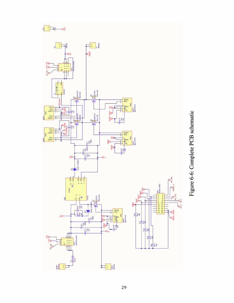
29

6.1 Trace Width Design
The maximum expected current in the power circuit was 10 A. Therefore, the minimum
acceptable trace width (accounting for a tolerance in current of 15%) for 1 oz copper with 200 C
temperature rise was calculated to be 4.63 mm.To meet this minimum requirement for power
circuit, polygons traces were used to supply power. This minimum was met for the core traces in
the power circuit. For traces with 5 A of current, the minimum trace width was 1.79 mm. The
control circuits carry significantly less current (due to the large values of the step down resistors).
The calculations for the trace width are shown in Appendix C.
6.2 Selection of Component Style and Placement of Components
During the PCB design process, attention was paid to the selection of components, and
their placement on the board. These design decisions are outlined in this section.
Through hole components were selected, as opposed to surface mount. Through hole
components are significantly easier to desolder. This provided the freedom to remove and replace
components such as resistors, capacitors and IGBT’s, which simplified the testing process.
Custom footprints were designed for several components, including the IGBT’s, power
capacitors, transformer, current sensor, isolators, heat sinks, gate drivers, and the inductor. These
footprints are shown in appendix D.
Attention was paid to the placement of components relative to each other. The trace
lengths were kept as short as possible to minimize the effects of parasitic inductances. Heat sinks
were placed directly next to each IGBT/ MOSFET to allow proper heat dissipation. Sufficient
space was also provided between each IGBT/Heat Sink pair, as well as between the IGBT’s and
gate drivers. This was done in an effort to prevent the IGBT’s and gate drivers from overheating.
Two planes of signal ground were placed in both layers to reduce the supplied gate signal
noise. Capacitors were placed in parallel with low power inputs to maintain input power to
devices. A 15 V supply was used to supply power to the board. Two voltage regulators were used
to supply 3.3V and 5V.
Several additional pads were added to the PCB to allow for testing and debugging.
6.3 Selection of Number of Boards
All components and design stages were included on one PCB. One alternative considered
was housing the power circuits on one PCB and the control circuits on a second PCB. However,
this required transmitting high power signals from one board to another. The design with one
PCB also provided a more compact design, with a lower cost.
30

6.4 Completed PCB
The completed PCB design is shown in figure 6-7.
Figure 6-7: Completed PCB Design
The fully populated PCB is shown in figure 6-8. The DC-DC converter is boxed in red.
The DC-AC inverter is boxed in cyan. The DC link capacitor is boxed in green. The control
circuits are boxed in pink. The input (panel) is boxed in purple. The output (grid) is boxed in
black. The components not included in any of the boxes are the current sensors and the isolators
(all blue components).
Figure 6-8. Fully populated PCB
31

Modifications were made to the PCB after it was received. The inductor value was
modified after the PCB design was completed. Therefore the inductor was soldered to perf board,
which was subsequently connected to the PCB. Additionally, two of the traces burnt out so
external jumpers were added.
32

Chapter 7- Controls and Microcontroller Programming
Prior to testing the high power design on the PCB, microcontroller code had to be
developed to implement the control algorithms. This sections describes the algorithms used to
develop the microcontroller code. There were three firmware based controllers used for this
project. The first controller was the maximum power point tracking. The second controller was
for the DC-AC current control and the third controller was used to regulate the DC link voltage at
200 Volts. A physical circuit was also developed to add dead band time to the pulse edges for the
pulse width modulation outputs. All the controller code was developed using blocks in Simulink.
The code was then exported to the microcontroller.
7.1 Maximum Power Point Tracking
The irradiance on solar panels changes with the time of day and amount of cloud cover,
among other factors. The microcontroller needs to be able to accommodate for these changes and
keep the system operating at the maximum power point. Maximum power point tracking code
was used to adjust the system parameters to the maximum power point out of the PV panel
simulator, and keep the output panel voltage steady at that level. This was accomplished by the
microcontroller reading in the panel voltage and current (PANEL_V and DC_I from the PCB
connector). The panel power and the panel voltage were then compared to the respective values
from the previous time point. The change in power over the change in voltage (dP/dV) was used
to determine whether to increase or decrease the voltage. dP/dV was then integrated, which gave
an updated voltage reference. The voltage reference was then fed to a PI controller, which output
an updated duty cycle for the pulse width modulation. The final parameter set for the PI controller
is shown in table 7-1.
Table 7-1: PI Parameters for MPPT
Parameter Value
Proportional Gain (Kp) 0.008
Integral Gain (Ki) 10
Derivative Gain (Kd) 0
The overall code for the maximum power point tracking is shown in figure 7-1.
33
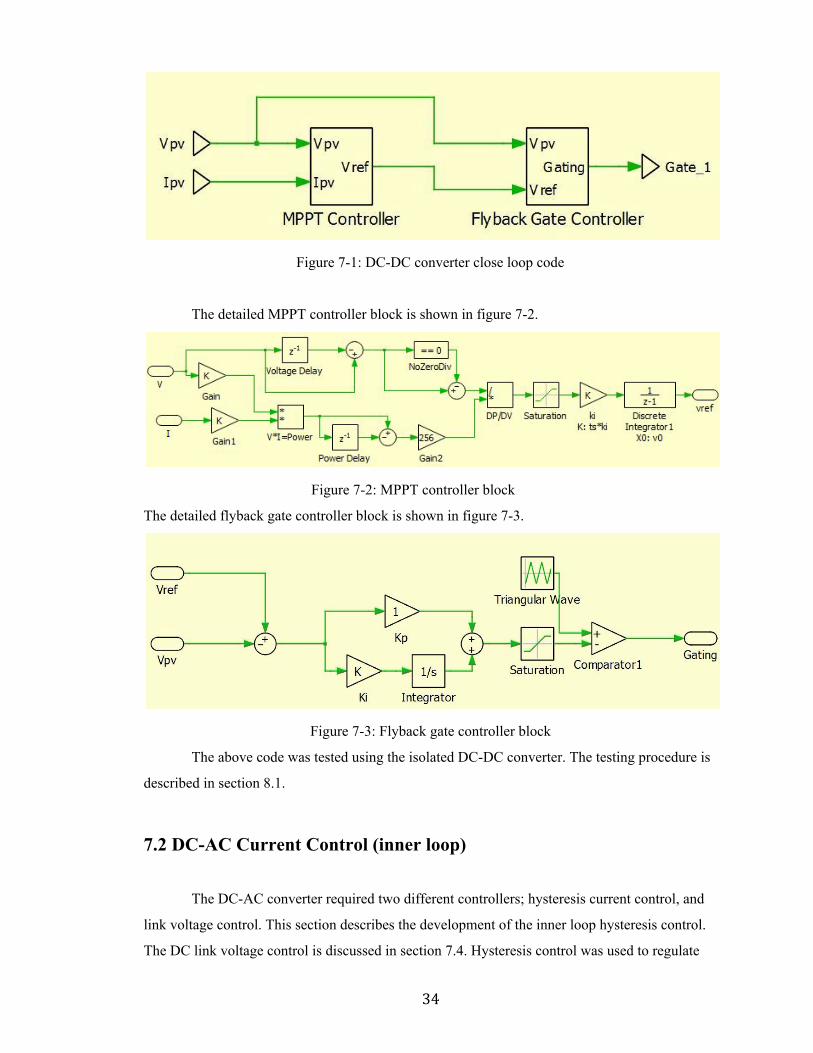
Figure 7-1: DC-DC converter close loop code
The detailed MPPT controller block is shown in figure 7-2.
Figure 7-2: MPPT controller block
The detailed flyback gate controller block is shown in figure 7-3.
Figure 7-3: Flyback gate controller block
The above code was tested using the isolated DC-DC converter. The testing procedure is
described in section 8.1.
7.2 DC-AC Current Control (inner loop)
The DC-AC converter required two different controllers; hysteresis current control, and
link voltage control. This section describes the development of the inner loop hysteresis control.
The DC link voltage control is discussed in section 7.4. Hysteresis control was used to regulate
34

the current sent to the grid, at the output of the DC-AC inverter stage. Hysteresis control, also
known as bang-bang control, is a closed loop control method that switches between two limits
[17]. Hysteresis control was selected, as opposed to PID control, in order to eliminate the need to
tune the parameters of the PID controller. A sine wave acted as the current reference signal in the
MCU internally, to compare the I_out and I_ref. The control program used for hysteresis control
is shown in figure 7-4. The gate signal output is then sent to the deadband circuit described in
section 7.3.
Figure 7-4: Hysteresis control loop
The hysteresis current control was tested using the DC-AC converter. The testing
procedure is described in section 8.2.
7.3 Deadband Circuit
The current controller code for the DC-AC inverter required pulse width modulation
signals (with varying duty cycles) to be sent to the four IGBT’s. Dead time had to be added to the
pulses to ensure that the four IGBT’s were not on simultaneously. A circuit was used to produce
the required dead band [18]. The circuit schematic is shown in figure 7-5.
Figure 7-5: Deadband circuit [18]
A 74LS14 was used for the inverter. The 74LS14 is a Schmitt trigger. The Schmitt trigger
35

produced sharp edges and was resistant to bouncing on the edges, which helped to produce
smooth pulses. The resistor values were 820 Ω and 1 kΩ, and the capacitor values were both 2.7
nF. The different resistor values were required to produce even deadbands on both the rising and
the falling edge. These values produced dead time of 1 us on each edge. The results can be seen in
the scope trace in Fig 7-6.
Figure 7-6. Output of dead time circuit yellow is V1 and the green is V2
In Figure 7-5, Vin was the output from the microcontroller. V1 and V2 were the two
output signals, which have dead time between them. V2 is the inverse of V1. This difference is
due to the fact that two inverters were used at the output of V1, while only one inverter was used
at the output of V2. V1 was then sent to two of the IGBT’s, and V2 were sent to the other two
IGBT’s.
7.4 DC Link Voltage Control (outer loop)
A PID controller was used for the DC link voltage control. The DC link voltage was read
into the microcontroller, after being stepped down by the circuit described in section 5.3. This
voltage level was then compared to the scaled reference level of 200 V. The difference was fed
into a PID controller. The schematic is shown in figure 7-7.
36
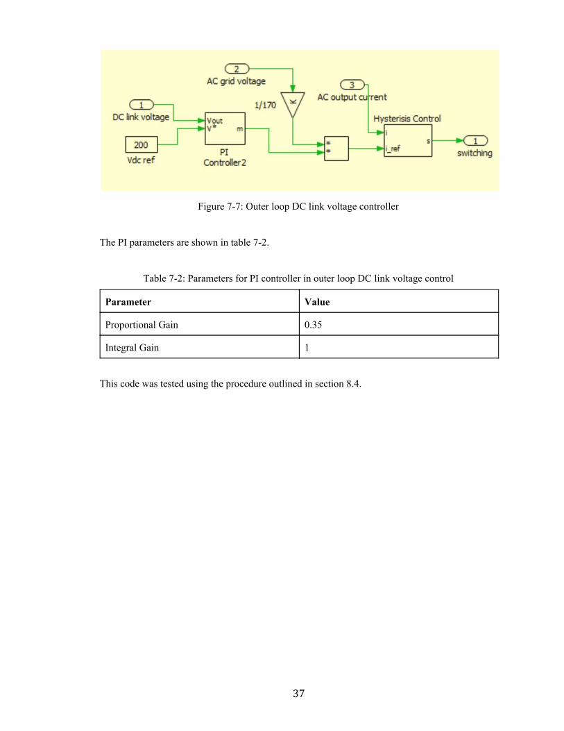
Figure 7-7: Outer loop DC link voltage controller
The PI parameters are shown in table 7-2.
Table 7-2: Parameters for PI controller in outer loop DC link voltage control
Parameter Value
Proportional Gain 0.35
Integral Gain 1
This code was tested using the procedure outlined in section 8.4.
37

Chapter 8- Integration of Subsystems This chapter discusses the procedures that were used to test the PCB (described in chapter
6) in conjunction with the microcontroller code (described in chapter 7). The integration of
subsystems was broken down into four main stages: testing the DC-DC converter with maximum
power point tracking, testing the DC-AC converter with open loop controls, testing the DC-AC
converter with current control, and testing the DC-AC converter with DC link control. These tests
are described in this chapter.
8.1 DC-DC Converter with Maximum Power Point Tracking
For this test, the DC-DC converter was tested with the maximum power point tracking
microcontroller code. The DC-DC converter components (including the input capacitor,
transformer, MOSFET, diode and link capacitor) were soldered to the PCB. In order to test the
DC-DC converter in isolation from the DC-AC inverter, a 200 ohm load was connected in
parallel with the DC link capacitors. A PV simulator was connected to the input of the DC-DC
converter. This testing setup is shown in the block diagram in figure 8-1.
Figure 8-1: Block diagram for DC-DC converter test with MPPT
The complete system setup is shown in figure 8-2. The load is boxed in green. The
DC-DC converter is boxed in pink. The PV simulator is boxed in blue and the DC link voltage is
boxed in yellow.
38

Figure 8-2: Setup for DC-DC converter test with maximum power point tracking
The final set of parameters used for the PI controller are shown in table 5. The D controller was
not used.
Table 8-1: PI parameters in Simulink for maximum power point tracking
Parameter Value
Proportional Gain 0.08
Integral Gain 10
The maximum power point tracking was tested for irradiance levels ranging from
50%-100% of maximum irradiance. The output plots of the maximum power point tracking is
shown in figure 8-3. The three data points represent irradiance levels of 50%, 75% and 100% of
maximum irradiance. The maximum voltage in this case was 28 Volts. The voltage at the
maximum power point was approximately 75% of the maximum voltage, which is consistent with
the expected voltage level at the maximum power point.
39

Figure 8-3. Measured maximum power point tracking at varying irradiance levels
This testing stage verified that the design requirement for maximum power point tracking
was successfully met. This test was also used to calculate the efficiency of the DC-DC converter
stage, which was 91%.
A simulation was completed in matlab which utilized the diode equation to model the
solar panel emulator. The parameters in the diode equation were estimated based on the
characteristics measured from the PV emulator. The Matlab code is shown in appendix E. The
simulated PV curves for irradiance levels of 100%, 75% and 50% are shown in figure 8-4.
Figure 8-4: Simulated PV curves at varying irradiance levels
40

The measured and simulated maximum powers (and their accompanying voltage level)
for each irradiance level are summarized in table 8-2. The average percent difference between the
measured and simulated maximum powers was 3.4%. The average percent difference between the
voltage levels at the maximum powers was 7.6%. Some sources of discrepancies are likely due to
limitations of the model that was used to represent the solar panel, and as well as the
measurement equipment.
Table 8-2: Differences in measured and simulated maximum power
Irradiance Level (%)
Measured Maximum Power (W)
Simulated Maximum Power (W)
Percent Difference (Power)
Measured Voltage at Max Power (V)
Simulated Voltage at Max Power (V)
Percent Difference (Voltage)
100 21.61 21.90 1.33% 24.00 23.61 1.64%
75 15.10 16.4 8.25% 22.50 23.04 2.37%
50 8.50 8.54 0.47% 18.19 22.00 18.95%
The close match between the measured maximum power points and the simulated PV
curves indicates that the maximum power point tracking algorithm was successful.
8.2 DC-AC Converter with Open Loop Controls
After completing testing of the DC-DC converter with closed loop controls (for
maximum power point tracking), the DC-AC inverter was tested with open loop controls. The
open loop code provided a sinusoidal pulse width modulated signal to the four MOSFET’s in the
full bridge inverter. This test served two functions. The first purpose was to verify functionality of
the DC-AC converter at high power. The second function was to test the filter. For this test the
diode connecting the DC-DC converter to the DC-AC inverter was removed (to isolate the
DC-AC stage). The input (DC link voltage) to the DC-AC inverter was 200 Volts, and the output
was connected to a 230 ohm load. This testing setup is shown in figure 8-4.
41

Figure 8-5. DC-AC converter test with open loop controls
The initial test with MOSFET’s resulted in the MOSFET’s overheating. Therefore, the
MOSFET’s were replaced with IGBT’s, which have a reverse diode. The IGBT’s had the same
pin out as the MOSFET’s and could be driven using the same gate drivers. This simplified the
replacement process. The filter was also changed to a third order filter, instead of a first order
filter. The third order filter used two series inductors and a shunt capacitor. The final parameters
for the filter are shown in table 8-3.
Table 8-3: Output filter parameters
Parameter Value
First Series Inductor 1 mH
Shunt Capacitor 2.2 uF
Second Series Inductor 1 mH
With a 200 Volt DC input, the output voltage (measured across the 230 ohm load) was
330 volts peak-peak, as shown in figure 20. 330 volts peak to peak is equivalent to 116 volts rms,
as shown in figure 8-6. This falls within the acceptable range of 120 Vrms ± 5% (the range is 112
Vrms – 126 Vrms). The output voltage specification was met.
42

Figure 8-6: 330 V peak to peak output voltage with open loop controls
The output current was sinusoidal, as shown in figure 8-7. The spikes in the figure are
most likely due to the current sensor that was used to acquire the measurement, and not due to the
actual current value.
Figure 8-7: Output current with open loop controls
This test successfully met two design specifications: output voltage level, and sinusoidal
output current. Additionally, the frequency is 62 Hz. This matches the required output frequency
of approximately 60 Hz.
This test was also used to test the maximum power and the efficiency of the DC-AC
inverter stage. For the efficiency test, the input voltage and current are shown in figure 8-8. The
the input power was 178.4 Watts.
43

Figure 8-8: Input voltage and current
The output voltage and current are shown in figure 8-9.
Figure 8-9: Output voltage and current for open loop DC-AC testing
As seen from figure 8-9 the output voltage was 114 Vrms, and the output current was
1.46 A rms (note that the probe had 10x magnification). Therefore, the output power was 166.44
Watts. This measurement met the design specification for maximum power over 100 W. The
efficiency was 93%. Combined with the DC-DC efficiency of 91%, this resulted in an overall
44

efficiency of 85% which met the design specification of efficiency over 80%.
8.3 DC-AC Converter with Closed Loop Current Control
After testing the DC-AC Inverter with open loop controls, it was tested with closed loop
hysteresis controls. The goal of the hysteresis control loop was to ensure that the current injected
to the grid was sinusoidal. The hysteresis control loop was tested by connecting a 200 V DC
source to the input of the DC-AC converter. A 200 ohm resistor was connected to the output of
the load, rather than the grid. In this stage, the Hysteresis control for the DC-AC inverter stage
was implemented and tested. The setup is shown in figure 8-10.
Figure 8-10: AC current control testing setup
An external 1.65V DC was provided to bias the output current signal from the AC current
sensor (the current sensor output a voltage sine wave). Therefore, the output signal was always in
the range of 0-3.3V. In order to ensure that the output current was always the same as the
reference signal, the output of the relay was the gate signals being sent to the IGBTs. The system
was tested with a range of input voltages from 20 Volts to 200 Volts. The system produces a
sinusoidal output current for input voltages ranging from 60 Volts- 200 Volts. This is due to the
fact that the delta I is fixed, and if the current is not big enough, the control was not accurate.
However the target value for the DC link voltage was 200 Volts, so this test met all necessary
design specifications. The output current was measured using a current sensor, for input DC link
voltages ranging from 60 Volts to 200 Volts. The output current for a DC link voltage of 120
Volts is shown in figure 8-11. The output current is shown in blue, and was 2.1 A peak-peak. The
output voltage is shown in green and was 104.7 V peak-peak. As is seen in the image, the output
current is a regulated sinusoid. This test indicated that the current controller was functioning
properly. The goal of the controller was to produce a sinusoidal current, that is in phase with the
45

output voltage. Both of these criteria are met. Therefore, this test successfully met the output
current control design requirement.
Figure 8-11: Output for testing grid current control
8.4 DC Link Voltage Regulation and Grid Connection
The final stage of testing was regulating the DC link voltage. For this stage of testing, a
200 ohm load was applied to the input of the DC-AC converter (the DC link voltage was then
measured across the load). The grid was connected to the output of the DC-AC inverter. the
current control code and the DC link voltage control code were then applied to the DC-AC
converter. The purpose of this test was to ensure that the outer loop DC-AC controls successfully
regulated the DC link voltage. The complete setup for this test is shown in figure 8-12. The load
is boxed in purple, the DC-AC converter is boxed in blue and the grid voltage is boxed in green.
The microcontroller is not shown in the photo.
46

Figure 8-12: Setup for testing DC link voltage control
The DC link voltage controller was able to regulate the voltage at 15 Volts. The output
from this test is shown in figure 8-13. In this figure, the green waveform is the DC link voltage
which is stable at 15 V nominal.
Figure 8-13: Output of DC link voltage testing
This test validated the algorithm used for testing the DC link voltage control at low
voltage levels. This test also demonstrated that the microinverter can be successfully connected to
the grid. The integrated control system was not tested. However, all design requirements were
met through the subsystem tests.
47

Chapter 9- Summary of Results and Conclusions 9.1 Summary of Design Specifications
The final design results are shown in table 9-1.
Table 9-1: Final design results
Feature Target Value Actual Results Specification
Met Maximum Power 100 W or more 166 W Yes (exceeded)
Minimum Power 50 W or less 18 W Yes (exceeded)
Temperature Range
-30°C to 50°C (operating temperature range for components)
All components have operating temperatures in range of -40°C to 85°C (Appendix F)
Yes (exceeded)
Maximum Power Point Tracking
Extract maximum output power from the solar panel at different sunlight and temperature conditions
Implemented using microcontroller
Yes
DC Voltage Step Down Output Voltage< 3.3 V
Max output voltage of 2 V
Yes
AC Voltage Step Down Output Voltage < 3.3 Vp-p
Max output voltage of 2.4 V p-p
Yes
Voltage Requirements
DC link voltage
The nominal value of the voltage link the DC-DC and DC-AC stage will be 200 V
200 V with open loop controls
Yes
Grid voltage 120 Vrms +/-5% at 60Hz
116 Vrms (120 Vrms – 3.3%)
Yes (exceeded)
Current Control Grid current must be sinusoidal and in phase with grid voltage
Sinusoidal and in phase with grid voltage
Yes
Efficiency Average efficiency of >80%
DC-DC efficiency= 91% DC-AC efficiency = 93% Overall efficiency= 85%
Yes (exceeded)
48

9.2 Added Value Features
This project had several added value features not included in the original design
specifications. The original design required two PCB’s: one for the power circuit and one for the
control circuit. The final design used only one PCB, which housed both the power and control
circuits. This added feature reduced the size of the microcontroller, while also decreasing the
production cost. Another value added feature was testing the complete design with a PV
simulator. The original plan was to use an input DC voltage source. In addition to designing the
main power circuit (DC-DC converter, DC-AC inverter) and the controls circuits, a circuit for
adding dead time was also designed, which can be applied to future projects. 9.3 Future Work
Several possible expansions for the projects were identified. Testing of the microinverter
was completed by connecting a PV simulator to the input of the DC-DC converter. The complete
microinverter design could also be tested using a physical solar panel. Several potential
improvements were also identified for the overall system. Additionally, a protective case could be
designed for the microinverter. This would be useful if the inverter was being used outside, where
it would be exposed to elements such as snow, rain and extreme temperatures.
9.4 Conclusion
All design specifications, except for efficiency, were successfully achieved in both
simulation, and physical testing with a PCB and microcontroller code. The maximum and
minimum power were within the acceptable ranges, the maximum power point tracking was
successful, and the output voltage and current requirements were met. Additionally, all core
components had operating temperatures within the acceptable range. Several added value
features were also included in the design. The final project deliverables were a complete set of
microcontroller code and a fully populated PCB.
49

Bibliography 1. Canada- A Global Leader in Renewable Energy. Energy and Mines Ministers
Conference. Yellowknife, August 2013. 2. About Renewable Energy. Natural Resources Canada. June, 2016. 3. Nate Damaschke. Solar Power . University of Manitoba 4. Rezaei. M et al. A High Efficiency Flyback Micro-Inverter With a New Adaptive Snubber
for Photovoltaic Applications. IEEE Transactions on Power Electronics. Volume 21, Issue 1. Pages 318-327. 2016.
5. Cha Woo-Jun et al. Highly Efficient Microinverter With Soft Switching Step-Up Converter and Single Switch Modulation Inverter. IEEE Transactions on Industrial Electronics. Volume 62, Issue 6. Pages 3516-3523. 2015.
6. Dino Green. Microinverters vs String Inverters. Renewable Green Energy Power. March 2013.
7. S. Saravanan and S. Thangavel. A Simple Power Management Scheme with Enhanced Stability for a Solar PV/Wind/Fuel Cell/Grid Fed Hybrid Power Supply Designed for Industrial Loads. Journal of Electrical and Computer Engineering, Volume 2014, Article ID 319017, 18 pages
8. Meneses. D. et Al. Grid-Connected Forward Microinverter With Primary Parallel Secondary Series Transformer. IEEE Transactions on Power Electronics. Volume 30, Issue 9. Pages 4819-4830. 2015.
9. Maximum Power Point Tracking. Wikimedia. 2017 10. User’s Guide for Digitally Controlled Solar Micro Inverter Design using C2000 Piccolo
Microcontroller. Texas Instruments . Page 3. February, 2016. 11. Navigating the Boost Converter’s Vulnerability with Alternative Power Conversion
Topologies. All About Circuits. November, 2015. 12. Flyback Converter. Wikimedia. 2017. 13. Flyback Converter. Plexim . 2016. 14. H Bridge Operation. Wikimedia. 2017 15. Plexim User Manual. 4th edition. PLECS- The Simulation Platform for Power Electronic
Systems. Switzerland, 2016. 16. Altium Designer Tutorial. Altium Designer. 2016. 17. C. Ho, V. Cheung and H. Chung, “Constant-frequency hysteresis current control of
grid-connected VSI without bandwidth control”, IEEE Trans. on Power Electronics, Vol. 24, No. 11, pp. 2484 – 2495, Nov. 2009.
18. External PCB Max Current. EEWeb. 2017.
50

Appendix A- Complete Team Budget The completed team budget is shown in table A-1.
Table A-1: Final budget
Note:
1. The microcontroller and magnetic core were borrowed from Dr. Carl Ho. They will be
returned after the project presentation.
2. The Flyback transformer (58PR6962) was sponsored by VITEC Electronics
Corporation.
3. Other small components, such as wires, connectors, and low power passive
components were provided by the tech shop.
51

Appendix B- Inductor Design
It was difficult to find an inductor with the specifications required for this inverter.
Therefore, a inductor was custom made. The design procedure is included in this appendix.
The selected magnetic core was AMCC 10, which has a high current saturation limit and
a relatively small size. The wire type was AWG 16. This wire was selected because of its’ high
current carrying ability and small cross section area. The data sheet for AMCC10 is shown in
figure B-1.
Figure B-1: Data sheet of AMCC10
The specifications for AWG 16 are shown in table B-1.
Table B-1: Data table of AWG 16
Parameter Value
Diameter 1.291mm
Cross Section Area 1.31 mm2
Resistance per length 13.17 mΩ per meter
The required design specifications are shown in table B-2.
52

Table B-2: Required inductor design specifications
Variables Specifications
Inductance 4mH
Frequency 20kHz
Designed Current 2A
Current Ripple 25%
Turns Less than 150 turns
Filling Factor Slightly less than 0.4
Loss Under 5W under maximum current condition
The calculations used to determine the inductor parameters are shown below.
ean T urn Length ×(a b) .114 m M = 2 + d + 2 = 0 [1]
I ×I ×Current Ripple .707 A ∆ = √2 max = 0 [2]
Choose the length of airgap being 1mm, the number of turns, N, can be calculated as:
20 turns N = √ 4π×10 ×a×d−7Airgap Length×L = 1 [3]
The filling factor
.303Kcu = NCorss Section Area of the Wire×Wa = 0 [4]
The flux density is given by:
Bac = Airgap Length4π×10 ×N×∆I−7
[5]
The maximum core loss is:
.5×f ×B ×W eight of the Core .448W P core = 6 1.51ac1.74 = 2 [6]
The maximum copper loss is:
×MT L×N×Resistance per Meter .722W P cu = I2 = 0 [7]
Maximum power loss is:
.17W P loss = P core + P cu = 3 [8]
53

The actual inductance produced was 3.7 mH, the power loss of the inductor was 3.17W under the
worst condition, and the filling factor is about 0.303 which is close to the standard value of 0.4.
54

Appendix C- Calculation of Trace Width The calculations for the trace width are shown in figure C-1.
Figure C-1: Trace width calculation [18]
55

Appendix D- Custom PCB Footprints
Several components used in the design did not have available footprints and schematics in the Altium library. Several of the custom component footprints and schematics are shown in this appendix.
The current sensor used in the design was 398-1007-ND. It had nine pins with 0.7mm pin width. The component had dimensions of 14.93x33.2. The current sensor footprint design and schematic design are shown in figure D-1.
Figure D-1 : Current sensor footprint and schematic
Four power capacitors were used in the design. The Altium footprint was created to match the size of the capacitor. The hole diameter was 3.048mm and the pad diameter was 4.064mm. These dimensions were selected to accommodate wider capacitor pins. The capacitor footprint is shown in figure D-2.
Figure D-2 : Power capacitor footprint
The flyback transformer used in the design had 3.57mm diameter pins on the low voltage side. As a result, larger holes with pads were selected for the design of the footprint. The transformer footprint and schematic are shown in figure D-3.
56

Figure D-3 : Transformer footprint and schematic
The gate drivers in the design were custom built gate drivers. Measurements were taken with a ruler to measure pin diameters and the space between them. The gate drivers were mounted vertically. The gate driver schematic and footprint are shown in figure D-4.
Figure D-4: Gate driver footprint and schematic
Two different isolators were used in the design. Both of them had different pin maps and footprints. As a result, two sets of Altium footprints and schematics were designed. The isolator footprints and schematics are shown in figure D-5.
57

Figure D-5: Voltage isolator footprint and schematic
Five heat sinks were used in the design. The heat sink footprint was designed in Altium. The size of the heat sinks were selected to fit around the IGBT footprint. The heat sinks were selected to match the outer dimensions of the IGBT. The heat sink footprint is shown in figure D-6.
Figure D-6: Heat sink footprint
58

Appendix E- Simulated PV Curves The code used to simulate PV curves are shown in figure E-1.
Figure E-1: Code to simulate PV curves at varying irradiance levels
59

Appendix F- Operating Temperatures of
Components The design specification was to have an operating temperature range for the core
components in the main power circuit of -30 degrees Celsius to 50 degrees Celsius. Table F-1
summarizes the operating temperature ranges for each component in the main power circuit. All
components have an operating range of at least -40 to 80 degrees Celsius.
Table F-1: Operating range of core components
Component Minimum Temperature (degrees Celsius)
Maximum Temperature (degrees Celsius)
Transformer -40 125
DC Link Capacitor -40 85
Diode Not specified 225
MOSFET Not specified 260
IGBT -55 150
60