design and implementation of a decompression engine...
TRANSCRIPT

Chapter 1 Introduction
Design and implementation of a decompression
engine for a Huffman-based compressed data cache
Master’s Thesis in Embedded Electronic System Design
LI KANG
Department of Computer Science and Engineering
CHALMERS UNIVERSITY OF TECHNOLOGY
Gothenburg, Sweden, 2014

2
The Author grants to Chalmers University of Technology and University of Gothenburg
the non-exclusive right to publish the Work electronically and in a non-commercial
purpose make it accessible on the Internet.
The Author warrants that he/she is the author to the Work, and warrants that the Work
does not contain text, pictures or other material that violates copyright law.
The Author shall, when transferring the rights of the Work to a third party (for example a
publisher or a company), acknowledge the third party about this agreement. If the Author
has signed a copyright agreement with a third party regarding the Work, the Author
warrants hereby that he/she has obtained any necessary permission from this third party
to let Chalmers University of Technology and University of Gothenburg store the Work
electronically and make it accessible on the Internet.
Design and implementation of a decompression engine for a Huffman-based compressed
data cache
Li Kang
© Li Kang January 2014.
Supervisor & Examiner: Angelos Arelakis, Per Stenström
Chalmers University of Technology
Department of Computer Science and Engineering
SE-412 96 Göteborg
Sweden
Telephone + 46 (0)31-772 1000
[Cover: Pipelined Huffman-based decompression engine, page 8.
Source: A. Arelakis and P. Stenström, “A Case for a Value-Aware Cache”, IEEE
Computer Architecture Letters, September 2012.]
Department of Computer Science and Engineering
Göteborg, Sweden January 2014

i
Abstract
This master thesis studies the implementation of a decompression engine for Huffman
based compressed data cache. Decoding by traversing a Huffman tree bit by bit from the
root is straightforward but has many implications. In order to store a Huffman tree, it
requires too much memory resources, and the compressed memory content needs to be
decompressed and recompressed when encoding changes. Besides, it may be slow and
has varying decoding rate. The latter problem stems from that there is no specific
boundary for each Huffman codeword. Among Huffman coding variations, Canonical
Huffman coding has numerical features that facilitate the decoding process. Thus, by
employing Canonical Huffman coding and pipelining, the performance of the
decompression engine is promising. In this thesis, the specific design and implementation
of the decompression engine is elaborated. Furthermore, the post-synthesis verification,
time and power analyses are also described to show its validity and performance. Finally,
the decompression engine can operate at 2.63 GHz and the power consumption is 51.835
mW, which is synthesized with 28nm process technology with -40℃ and 1.30V.

ii

iii
Acknowledgements
I am very grateful for all the support and advices I have received. This project could not
have been realized were it not for the help and support of a great many people.
First and foremost, I would like to appreciate my advisors, PhD Candidate Angelos
Arelakis and Professor Per Stenström. They are very pleasant to work with and helped
me a lot with invaluable feedback.
I would like to acknowledge the helps of Professor Per Larsson-Edfors, Docent Lars
Svensson, Alen, Dmitry, Kasyab, Bhavishya, and Madhavan, who shared many technical
knowledge and experience with me. Also, I greatly appreciate many IT supports from
Peter Helander, Rune Ljungbjörn
A special thanks to my parents and girlfriend, who helped me out of many
difficulties in life and provided me with warm encouragement.
I highly appreciate for the effort that our thesis opponents, Roozbeh Soleimanifard
and Reza Zakernejad made. Their criticism and their questions opened our eyes for weak
points in our work that we had missed.
Li Kang, Gothenburg Jan, 2014

iv

v
Content
Abstract ................................................................................................................................ i
Acknowledgements ............................................................................................................ iii
Content ................................................................................................................................ v
List of abbreviations .......................................................................................................... ix
1 Introduction ................................................................................................................. 1
2 Theory .......................................................................................................................... 3
2.1 Huffman coding.................................................................................................... 3
2.1.1 Information entropy ...................................................................................... 3
2.1.2 Huffman coding ............................................................................................ 3
2.1.3 Canonical Huffman coding ........................................................................... 4
2.2 Design Process ..................................................................................................... 5
2.3 Summary .............................................................................................................. 6
3 Design .......................................................................................................................... 7
3.1 Related work ........................................................................................................ 7
3.2 Huffman decompression engine ........................................................................... 8
3.2.1 Algorithm ...................................................................................................... 8
3.2.2 Impact of table sizes ...................................................................................... 9
3.2.3 An example ................................................................................................. 10
3.3 Summary ............................................................................................................ 11
4 Implementation .......................................................................................................... 13
4.1 Block diagram of the decompression engine ..................................................... 13
4.2 Decompression process ...................................................................................... 13
4.3 FIFO stage .......................................................................................................... 14
4.4 CD stage ............................................................................................................. 14
4.4.1 Address controller ....................................................................................... 15
4.4.2 Buffer unit ................................................................................................... 15
4.4.3 Barrel shifter ............................................................................................... 15
4.4.4 Comparator ................................................................................................. 17

vi

vii
4.5 VR stage ............................................................................................................. 17
4.6 Summary ............................................................................................................ 18
5 Synthesis and verification .......................................................................................... 19
5.1 RTL Synthesis .................................................................................................... 19
5.2 Verification Process ........................................................................................... 20
5.2.1 Testbench .................................................................................................... 20
5.2.2 Static timing analysis .................................................................................. 21
5.2.3 Stimulus generation .................................................................................... 21
5.2.4 Check the response ..................................................................................... 22
5.2.5 Configuration of the FIFO .......................................................................... 24
5.3 Summary ............................................................................................................ 24
6 Performance and Power Evaluation .......................................................................... 25
6.1 Performance ....................................................................................................... 25
6.1.1 Static timing analysis .................................................................................. 25
6.1.2 Critical paths ............................................................................................... 25
6.1.3 Design Variation ......................................................................................... 26
6.2 Power Analysis ................................................................................................... 27
6.2.1 Power definition .......................................................................................... 27
6.2.2 Test vectors setup ........................................................................................ 28
6.2.3 Power analysis based real and corner cases ................................................ 28
6.2.4 Power distribution among three stages ....................................................... 30
6.2.5 Power consumption for different DeLUT sizes .......................................... 31
6.2.6 Design variation .......................................................................................... 32
6.3 Energy Analysis ................................................................................................. 32
6.4 Summary ............................................................................................................ 33
7 Conclusion ................................................................................................................. 35
Bibliography ..................................................................................................................... 37

viii

ix
List of abbreviations
CD code detection
CHC Canonical Huffman coding
CT codewords table
CW codeword
DeLUT decode look up table
DIT decode information table
DUT design under test
FCW first codeword
FIFO first in first out
HDL hardware description language
LUT look up table
RAM random access memory
ROM read only memory
RTL register transfer level
SDF standard delay format
STA static timing analysis
VFT value frequency table
VR value retrieve


1
1 Introduction
Computer system performance depends on the memory system as well as the
processor microarchitecture. Conventionally, the optimization of the memory hierarchy is
focused on the average memory access time. However, power is a design constraint with
growing importance. In the work stations, the high end computers use powerful multi-
core processors with on-chip cache on the order of 10MBs and large off-chip memory on
the order of dozens of GBs, consuming considerable power. The problem is more severe
for the processors in mobile devices, like smartphones and tablets. In these devices, CPUs
are less performance-oriented, while the battery life is equally important for the users‟
experience. In such cases, 25% to 50% of the total power is consumed by the cache [1].
Thus, more attention should be drawn on both performance and power trade-off.
The power dissipation can be reduced by keeping the memory resources in a small
size. One way to do this while the performance is little or not affected is to employ data
compression. Therefore, the cache data are compressed before being stored and
decompressed before being accessed. The former operation is executed by an encoder
and the latter by a decoder. Therefore, an encoder and a decoder are required to be
integrated in the cache. Since decompression is on the critical path (requested cache data
by the processor must be decompressed) and may affect the cache hit time, the decoder‟s
design is highly constrained in terms of speed. In addition, the power dissipation
overheads caused by the encoder and decoder must be kept in low levels. Thus, the
architectural support for cache compression is highly constrained in both terms of
performance and power dissipation.
Several cache compression approaches have been proposed in the past: 1) Pattern-
based approaches that replace common patterns with fixed-width encodings [2] and 2)
dictionary-based approaches that keep commonly appeared values in a dictionary and
instead save a pointer to the dictionary [3]. Both pattern-based and dictionary-based
approaches have the characteristics of a simple design, relatively low decompression
latency but mediocre compression efficiency.
On the other hand, statistical-based approaches [4][5], such as Huffman coding,
have high compression potential at the cost of more complex design and possibly higher
decompression latency. The Huffman coding algorithm replaces data symbols (also
referred as data values) by variable-length codewords: short codewords are assigned to
more frequent values and longer codewords to less frequent values. Huffman coding is
generated by building the Huffman tree based on the frequency of occurrence of the data
values.

Chapter 1 Introduction
2
This thesis project targets design and implementation of a decompressor for a
Huffman-based compressed cache approach because decompression is more complex and
designing a decompressor without significantly penalizing the cache hit time is
challenging.
Decoding is a reverse process of encoding which traverses the Huffman tree bit by
bit starting from the root using the compressed data stream. Unfortunately, it has many
implications. In order to store a Huffman tree, it requires much memory resource, and the
memory needs to be updated when encoding changes. Besides, it is slow and has varying
decoding rate. This inefficiency stems from the fact that there is no specific boundary for
each codeword (CW), due to the variable length codeword nature of Huffman coding.
The approach is the following. The decoding problem can be divided in two phases:
1) Codeword Detection: a valid codeword is detected; 2) Value Retrieve: Using the
detected codeword, the associated value is retrieved. Canonical Huffman coding, can be
utilized instead to facilitate this two-phase process, as the generated codewords have the
numerical sequence property and can be more efficiently detected in the first phase. In
addition, these two phases can run independently concluding that the decoding process
can be actually pipelined in at least two stages, each one of which runs one decoding
phase. Consequently, by employing Canonical Huffman coding and pipelining, the
performance of the decompression engine is promising.
The methodological approach taken in the project to evaluate the design is the
following. The logic simulation and post-synthesis verification tool is Modelsim. The
synthesis and timing and power analysis tool is Synopsys Design Compiler. The process
technology employed is 28nm, provided by STMicroelectronics.
In the project, the following main results are found. The decompression engine can
operate at 2.63 GHz and the power consumption is 51.835 mW. In other words, in each
380 ps, it can derive a 32-bit decompressed value from the decompression engine.
In Chapter 2, the thesis firstly describes the theory behind Huffman-based data
compression. That is vital for the understanding of the decompress engine‟s structure.
Then, Chapter 3 introduces the design of the decompression engine, including the details
of the decompression algorithm. In Chapter 4, the specific implementation of the
decompression engine is represented. After the implementation, its synthesis and
verification process will be illustrated in Chapter 5. In order to verify the performance
and power dissipation of the design, the timing and power analysis are elaborated in
Chapter 6. Finally, in Chapter 7, the findings and insights from the thesis work will be
reviewed.

3
2 Theory
This chapter will provide the theoretical background that is necessary to understand
the Huffman coding process. It first introduces the entropy theory to understand the
superiority of Huffman coding. Then, it explains the Huffman encoding and decoding
process and presents the properties of Canonical Huffman coding. Finally, it describes the
compression process and the structure of the compressed cache block.
2.1 Huffman coding
2.1.1 Information entropy
In information theory, the Entropy [6] is used to express the uncertainty of a random
variable U that takes values in the setu . It is defined as
supp(P )
(U) ( ) log ( )U
U b U
u
H P u P u
(2.1)
where ( )UP denotes the probability mass function (PMF) of the U, b is only a unit
change, in this thesis, let it be 2, and where the support of ( )UP is defined as
supp( ) : ( ) 0U UP u P uu .
Take a symbol sequence as an example.
{ , , , , , , , , , , , , }u v w w x x y y y z z z z
There are five different letters; so that 3 bits are needed to describe each letter
originally in a fixed-width representation. By using equation (2.1), we can get its
Shannon entropy.
2 2 2 2
1 1 2 2 3 3 4 4( ) ( 1) (2 log 2 log log log ) 2.4116
13 13 13 13 13 13 13 13H u
It means at least 2.4116 bits are required for each letter to express such a sequence
without any loss. So the data compression ratio is 3 / 2.4116 = 1.244.
2.1.2 Huffman coding
Huffman coding is a lossless data compression algorithm with variable length codes
[7]. Given a set of data symbols and their occurrence frequency, the algorithm constructs
a set of variable length codewords (CW) with the shortest average length and assigns
them to the symbols. The shorter CWs are assigned to more frequent symbols, while

Chapter 2 Theory
4
longer CWs for less frequent symbols. Huffman coding is widely used in the multimedia
codec, like the MP3 and JPEG files.
Huffman coding is generated by building a Huffman tree according to the data
symbols‟ frequency distribution. Take the same symbol sequence in section 2.1.1 as an
example. The binary tree is constructed bottom-up and left-to-right. Firstly, the symbols
are sorted in ascending order of their probabilities. In every step, two leaves (symbols)
with the least probabilities are placed in the tree. Their parent node has the sum of the
probabilities of the two leaves. This step should be repeated until the root node, which
has the probability of 1. Figure 2.1 shows the process of the construction of Huffman tree
and its Huffman CWs.
u1/13
1 0
1 0
1 0
2/13
5/13
00:
(b) Huffman tree (c) Huffman code
z
1 0
4/13
v1/13
w2/13
x2/13
y3/13
z4/13
8/13
1 0
10:y
010:x
011:w
110:v
111:u
4/13:
(a) Probability
z
3/13:y
2/13:x
2/13:w
1/13:v
1/13:u
Figure 2.1 The construction of Huffman tree and Huffman codeword
After the tree is completed, ones and zeros are assigned to left and right branches
respectively. The ones and zeros can be assigned to right and left branches, respectively,
as well, but the assignment must be consistent. Then the coding for each value-symbol is
generated by traversing the tree from the root to the respective leaf. The CWs for the
symbols u, v, w, x, y and z are 1111, 1110, 110, 10, 0 respectively, as it is also depicted
in Figure 2.1(c). The average size of the code is 3 × 1 / 13 + 3 × 1 / 13 + 3 × 2 / 13 + 3 ×
2 / 13 + 2 × 3 / 13 + 2 × 4 / 13 = 2.4615 bit / symbol. It is close to the entropy.
Huffman coding generates prefix-free code words. That is to say, there is not any
CW is a prefix of another CW. The prefix property is crucial for the code detection, as it
would be impossible for the decompression engine to detect a valid codeword otherwise.
2.1.3 Canonical Huffman coding
Among many alternatives in Huffman coding, Canonical Huffman coding (CHC) is
a particular type with unique properties which facilitate both encoding and decoding
processes. Before generating the Canonical Huffman codewords, their length must be
first calculated. This information is provided by the Huffman tree by counting the number
of pointer jumps from the root to each leaf when traversing the Huffman tree [5]. Then

Chapter 2 Theory
5
the value-symbols are sorted in ascending order according to their code-length. The
Canonical Huffman codewords are generated in the following steps:
(1) The first value-symbol is assigned to codeword 0 (numerical value of the CW is
zero), represented by as many bits, as its code-length (say „len‟) determines.
(2) CWs with the same length are numerically consecutive.
(3) The first code word (FCW) of the length “len+1” can be calculated from the last
code word (LCW) of the previous length “len” by using the formula
FCW[len+1]=(LCW[len]+1)×2. If there is no valid codewords for this length, use
the formula FCW[len+1] = LCW[len]×2, and FCW[len+1] = LCW[len+1].
The CWs in Figure 2.1 can be transferred to be Canonical Huffman codewords by
following steps. The process is shown in Figure 2.2. The first value-symbol is z, its
length is 2 so its CW is “00” and the CW of y is “01”. Then the CW length increases by 1,
the FCW of length 3 is “100”, and it is assigned to x. Finally, w, v and u are assigned
with “101”, “110” and “111”.
00:
(a) Generic Huffman coding
z
10:y
010:x
011:w
110:v
111:u
00:
(b) Canonical Huffman coding
z
01:y
100:x
101:w
110:v
111:u
Figure 2.2 The transform from generic to Canonical Huffman code
2.2 Design Process
Architecture Behavior RTL Gate Place & Route
synthesis
Figure 2.3 Design levels for VLSI design
There are five levels in the digital integrated circuit design shown in Figure 2.3.
Firstly, architecture level determines the skeleton according to the demand analysis. At
this level, some structure parameters are defined, such as the number of stages will be
employed in the pipeline. Then, at the behavior level|, the design is prototyped to test its
feasibility. In order to accelerate this process, the behavior hardware description language
(HDL) is used in the prototype, without regard of the circuit. At the register transistor
level (RTL), structure HDL is used and it is synthesizable. From the RTL design
description, a synthesis tool is used to implement the design in the target process

Chapter 2 Theory
6
technology to generate a gate level netlist. The designs were iterated until functional,
performance, timing, area and power requirements were met. The final level is place and
route. It includes floor planning, power routing, clock tree synthesis routing and post-
route optimization and so on [8]. In this thesis, I will present the design at architecture
level, RTL level and gate level.
2.3 Summary
This chapter provided the essential background knowledge for the thesis.
(1) The Huffman code length is varying. No explicit CWs boundaries exist.
(2) The Canonical Huffman encoding will be used in the design.
(3) The design will be presented in architectural, RTL and gate level.

7
3 Design
This chapter will introduce the design of the decompression engine. Firstly, it
describes the related work about the Huffman decoder and discusses the algorithm used
in this thesis. Then, the algorithm is illustrated by an example of the codeword table and a
pipelined organization. Finally, the impact of the table size and the compression process
are presented.
3.1 Related work
The variable length decoding is more difficult to implement than the encoding
because the input to the decoder is a bit stream without explicit word boundaries.
Existing decoders can be classified into three approaches as follows:
(1) Serial Decoders: They traverse a Huffman tree to detect and retrieve each symbol.
This method has two problems. Firstly, since the input coded data stream is
compared to a binary tree bit by bit; the decoding rate is extremely low. Secondly,
Due to the variable CW lengths, the serial processing causes a variable output rate
[9].
(2) Parallel Decoders: For a constant output rate, the number of bits to be decoded at a
time should be equal to the longest CW length resulting in bit-parallel processing,
which guarantees that one CW is detected at each cycle. The variable length decoder
has to decode a codeword, determine its length, and shift the input data stream by a
specific number of bits that corresponds to the decoded code length, before decoding
the next CW. These are recursive operations that cannot be pipelined [10].
(3) Multiple-Symbol Decoders: Due to the variable CW length, a block of encoded data
stream may contain more than one code word. Multiple-symbol decoders employ
this property for short CWs [7]. However, the exponentially increasing control and
hardware complexity set constraints to implementations, especially, when large code
word tables are used [11].
In this thesis, we propose a decoder scheme which is (1) parallel and, (2) pipelined.
In addition, it deals with uncompressed codewords due to the fact that the symbol set (in
other words the number of possible cache values) is very large while the Value
Frequency Table (VFT) that establishes the frequency distribution of the values has
limited size, thus only a subset of values is actually compressible.

Chapter 3 Design
8
3.2 Huffman decompression engine
3.2.1 Algorithm
Figure 3.1 shows the pipelined organization of the decompression engine [4]. It
consists of two stages: Code Detection (CD) and Value Retrieve (VR).
In the CD part, a First Codeword Table (FCW) is used to detect a valid CW. The
numerical property defines that a CW of a specific length is valid, if it has a larger or
equal numerical value than the FCW of that length and smaller than the FCWs of any
larger length. This is done in the comparators while the priority encoder outputs the
matched length.
On the other hand, in the VR part, the valid CW is subtracted by a corresponding
item in Decompression Information Table (DIT). The result of the subtraction is used as
an index to derive the associated value from the Decompression Look Up Table (DeLUT).
≥
≥
≥
…...
…...FCW(3)
FCW(2)
FCW(1)Matched
Codeword
Priority
Encoder
Barrel
Shifter
Matched
Length
Decompression
Information
Table(DIT)
Value
Matching
Code RegDe-LUT
++
-
Figure 3.1 Pipelined organization of the decompression engine
The values are saved in consecutive locations of the DeLUT in code-length
ascending order and the detected CW is used to retrieve the value. The CWs are listed in
a codeword table (CT) with relevant lengths to indicate the FCW and DIT items. CT is
used during compression while all those tables (CT, FCW and DIT) are generated during
encoding generation. The generation of these tables is out of the scope of this thesis.
Table 3.1 shows an example of the DeLUT and CT. The DeLUT is on the left side, and
the CT is on the right side. The CWs in CT are not always listed with length ascending
orders.

Chapter 3 Design
9
Table 3.1 A small part of DeLUT and CT
Value Address Value CT
FCW DIT Codeword Length
A 000 A 0 1 0 0
B 001 B 10 2 10 01
C 010 C 110000 6 110000 101110
D 011 D 110001 6 110000 101110
E 100 E 110010 6 110000 101110
F 101 F 1100110 7 1100110 1100001
G 110 G 1100111 7 1100110 1100001
For example, there is a sequence 1100010…. The first valid CW is 1100012 because
it holds that 12>02, 112>102, 1100012 >1100002, 11000012<11001102. The matched CW
is 1100012, but 1100012 cannot be used as an index to retrieve the value. Since in the
DeLUT, the symbol D is stored in location 0112(3), the corresponding DIT item 1011102
(46) should be subtracted from 1100012 (49). Since the consecutive binaries are assigned
to the CWs with the same length, the same offset is subtracted from the CW with the
same length. The offsets are calculated during code generation and saved in the DIT.
Therefore, for Canonical Huffman codes, in addition to a DeLUT, a FCW table and a
DIT are required in decompression.
3.2.2 Impact of table sizes
Because the Huffman coding is based on occurrence frequency, a value frequency
table (VFT) is needed to keep record of the frequency of values in the cache. In the study
of Arelakis and Stenström[4], the optimum size for the VFT is obtained by comparing the
compression factor and the VFT size. From the results, the compression starts to degrade
when using a VFT of 16 KB or more. It means that the overhead to keep the values with
low frequencies in VFT is larger than the gain in compression. The Geometric-mean
curve shows that the VFT of 4 KB can achieve the highest compression rate. Therefore,
A VFT of 4KB is used in my design. Accordingly, the DeLUT is also 4KB. So the data
with low frequency will not be compressed. For the uncompressed data, a unique code
will be added as a prefix to be different from the encoded data. The unique code should
be short enough to decrease the overhead of the uncompressed data and prefix-free to
promise the correct decoding. This is the reason why this unique code is also generated
by the Huffman tree.

Chapter 3 Design
10
3.2.3 An example
0,0,0,0,0,0,2289,0,5695728,0,17276160,0,324,0,17241840,0
0 02289 1110111101
5695728 111011001017276160 uncompressed
324 110011017241840 11111011101010
1110111101 0 1110110010 1001
0 0 0 0 0 0 0 1 0 0 0 0 0 1 1 1 1 0 0 1 1 1 0 1 0 0 0 0 0 0 0 0
0
0 1 1 0 0 1 1 0 0 11111011101010 0 0 0 0 0 0 00
0 0 00 0 0
value codewords
(a)
(b)
(c)
Figure 3.2 The compression process of a cache block
Figure 3.2 illustrates coding generation and compression of a compressed cache
block. Part (a) is the 16 values in a cache block. Part (b) is the mapping from the original
values to Huffman encoded data. The values of (a) are replaced by the codewords of part
(b) and are concatenated to form part (c). Emphasis must be given in two points: 1) “1001”
at the end of first line in (c) is the unique code, indicating the next value is
uncompressed,(i.e. 17276160); 2) Zero filling is used at the end of the third line, “000000”
to specify boundaries between compressed blocks. Figure 3.3 shows the decompression
process of the compressed cache block.
00000011101111010111011001001001 00000001000001111001110100000000
00000011101111010111011001001001 00000001000001111001110100000000
00000011101111010111011001001001 00000001000001111001110100000000
00000011101111010111011001001001 00000001000001111001110100000000
00000011101111010111011001001001 00000001000001111001110100000000
00000011101111010111011001001001 00000001000001111001110100000000
00000011101111010111011001001001 00000001000001111001110100000000
00000011101111010111011001001001 00000001000001111001110100000000
00000011101111010111011001001001 00000001000001111001110100000000
Barrel-Shifter
Output
matched length = 1
matched length = 1
matched length = 1
matched length = 1
matched length = 1
matched length = 1
matched length = 10
matched length = 1
00000011101111010111011001001001 00000001000001111001110100000000
00000011101111010111011001001001 00000001000001111001110100000000
00000001000001111001110100000000
matched length = 10
matched length = 1
matched length = 32 01100110011111011101010000000000
D0 D1
New data is filled in D1Transfer D1 to D0
00000011101111010111011001001001 00000001000001111001110100000000unique code
Figure 3.3 Example of the decompression operations

Chapter 3 Design
11
At least two registers, D0 and D1 are required to store the input data. Then, the input
data are used by the barrel shifter. The number of bits for the barrel shifter is dependent
on the previous matched length. So the first output of the shifter is the D0. The matched
length on the left side belongs to the barrel shifter output in the diagram on the right side.
When a unique code is detected, the consecutive 32-bit is an uncompressed CW. When
D0 is used up, the data in D1 is transferred to D0, and a new data line is loaded in D1.
3.3 Summary
(1) Three tables are required for the decompression, FCW, DIT and DeLUT.
(2) Both of the FCW and DIT are 512 bytes, and the DeLUT is 4KB.
(3) Decompression is divided in two phases: code detection and value retrieve.

Chapter 3 Design
12

13
4 Implementation
This chapter elaborates the design and implementation of the decompression engine
in details. The example in the previous chapter (section3.2.3) is used to illustrate the
principles. Figure 4.1 shows the decompression engine which employs a three-stage
pipeline, i.e. FIFO, Code Detection (CD) and Value Retrieve (VR). Among there stages,
the CD is most important.
dataout
validre validwr
datain
re we
dataout datain
validre validwr
length length
dataoutdatain
we
clkrst
FI/CD CD/VR
Register in
pipeline
datain
wen
dataout
lineend lineend
validre validre
U1
FIFO
U2
CD
U3
VR
Figure 4.1 Pipelined design of the decompression engine
4.1 Block diagram of the decompression engine
The FIFO stage is actually a buffer that saves compressed bit sequence and controls
the transmission rate to the CD stage so that it will always has input and never suffers
from starvation due to different input and output rate. In the CD stage, a valid CW in the
encoded data from the FIFO stage is detected. Then, the matched length is given into the
VR. The VR uses the length and encoded data to retrieve the original value. During the
retrieve process, the FCW, DIT and DeLUT are employed, which have been explained in
Chapter 3. Between two consecutive stages, there are pipeline registers named by the two
stages. All ports for data transmission, like datain and dataout are 32-bit, the length is 5-
bit, and other flags are 1-bit.
4.2 Decompression process
Figure 4.2 shows a compressed cache block stored in a buffer with 32-bit rows.
1110111101 0 1110110010 1001
0 0 0 0 0 0 0 1 0 0 0 0 0 1 1 1 1 0 0 1 1 1 0 1 0 0 0 0 0 0 0 0
0
0 1 1 0 0 1 1 0 0 11111011101010 0 0 0 0 0 0 00
0 0 00 0 0
Figure 4.2 One compressed cache block for decompress

Chapter 4 Implementation
14
At the beginning, the upper line of the compressed cache block (see Figure 4.2) is
stored in the FIFO buffer, and then it is sent to the CD stage. In the CD stage, the first
step is to detect the valid CW. The first bit „0‟ is a valid CW and its length is 1. The
second step is to use the matched length to get offset and calculate the index. By using
the index, the original value can be retrieved. Then the rest 31 bits in the upper line
should be concatenated with the first bit in the second line to construct a new line and be
decoded. When it encounters the unique code, (can be any code of any length but “1001”
is the unique code assumed in all the examples of this thesis), the unique code should be
discarded, and the consecutive 32 bits constitute the uncompressed value. The process
continues until the cache block is decoded completely. Then the rest bits of the
compressed cache block will be discarded. In this example, the discarded bit sequence is
“0000000”. Afterwards, the decompression engine can start decompressing another cache
block. The three cases mentioned are marked with gray color, and they will be
specifically demonstrated in following parts.
4.3 FIFO stage
Since the length of the Huffman codes are varying, that is to say, in each cycle, the
matched length derived from the CD stage is less than or equal to 32 bits. So a FIFO
stage is needed to adjust the data imbalance.
The FIFO stage contains 8 rows and 32 bits for each row. The reason why 8 rows
are chosen will be explained in section 5.2.5. Among those interfaces, U1/validre
indicates the validity of the data in the FI/CD, and U1/re is the read request from the CD
to the FIFO. The data transition from FIFO to CD depends both on the FIFO and the
CD‟s states. The FIFO should have valid data stored in buffer rows, and the CD should
have the data request for further process. Otherwise, U1/validre becomes „0‟.
4.4 CD stage
The CD stage generates the matched length for a valid CW from the input data. Both
the CD and the VR stages are dependent on such length. Figure 4.3 shows the block
diagram of the CD stage.
Comparator
(FCW)
Address Controller
datain
dataout
length
validrewe
Buffer
Unit
(4×32)
Barrel
Shifter
Unique
Code
Detector
Figure 4.3 Block diagram of the CD stage

Chapter 4 Implementation
15
The CD stage works according to the following steps.
(1) After initialization, check buffer unit. If it is not full, the input data is written in it.
(2) The buffer unit should have at least two valid rows before it is readable. Then,
according to the read address, by using two rows in buffer unit and the previous
matched length, a new row is constructed in the barrel shifter.
(3) Check the constructed data row from barrel shifter, if it does not contain the unique
code, the row is used by the comparator to derive the matched length, and also be
sent out to the VR stage. If the unique code is found, the prefix will be discarded,
and the consecutive 32 bits become the new row and bypass the comparator. In this
case, the matched length is 32.
(4) Finally, the write, read address of buffer unit and shift length are adjusted according
to the matched length. If the buffer unit is not full, „U2/we‟ becomes „1‟, indicating
the buffer unit can accept more rows from FIFO stage. Otherwise, it is „0‟. If there is
a valid row offered to VR stage, „U2/validre’ is „1‟. Otherwise, it is „0‟.
4.4.1 Address controller
In the CD stage, the number of bits consumed is varying at each cycle. One row in
the buffer unit may be used for many cycles or used for only one cycle before the read of
next row. By using the matched length of the previous cycle, the address controller is to
coordinate the write and read address of buffer unit, and to calculate the shift length.
After each decoding process, it determines the status of the buffer unit.
4.4.2 Buffer unit
Since the length of the Huffman codes are varying, in each cycle, the length of bits
used by the decompression ranges from 1 to 36 (width of uncompressed value + 4-bit
unique code). Therefore a buffer unit is needed to adjust the data imbalance.
In Figure 3.3, two registers, D0 and D1 are used to store the input data. In the worst
case scenario, i.e. a series of uncompressed value, a 36-bit is parsed at each cycle. In
order to avoid buffer starvation, more than two register are used. It was found that a FIFO
structure with 4 registers is suitable. Besides, at least two rows in the buffer unit, in other
word, two registers should be valid before the decompression.
4.4.3 Barrel shifter
The FIFO and barrel shifter are used to construct a data row for unique code
detection and comparison. The shifter operation consists of one right shift, one left shift
and an OR logic.
(1) A variable named bitsadd is used to indicate the number of bits the row should be
shifted. It is calculated from the previous matched lengths.
(2) The radd indicates the read address. The shifter takes the row radd and radd + 1.The
row radd shifts left by bitsadd, and the row radd + 1 shifts right by 32 – bitsadd.

Chapter 4 Implementation
16
(3) Then these two rows are combined with OR logic. Figure 4.4 ~ Figure 4.7 show the
operations of the FIFO and the barrel shifter. The data in the Figure 4.2 is used here.
wadd radd 00000011101111010111011001001001radd
bitsadd=0
wadd
Initial 1st cycle
bitsadd=0
Figure 4.4 Initial status of the FIFO
Initially, the buffer unit is empty, and all addresses are zeros. At the first cycle, one
buffer row is written in the buffer unit, hence the write address wadd increases by 1.
00000011101111010111011001001001
00000001000001111001110100000000
radd
bitsadd=0
wadd
0
0000001000001111001110100000000
01100110011111011101010000000000
radd
bitsadd=1
wadd
0000011101111010111011001001001
0
3rd
cycle
dataout =
length = 12nd
cycle
dataout =
length = 1
00000011101111010111011001000101 00000011101111010111011001000101
Figure 4.5 2nd
and 3rd
cycle status of the FIFO
At the second cycle, the wadd continues increasing by 1, but the radd depends on
the result of the comparison. Since the bitsadd is 0, the barrel shift has no effect. The first
entire row is used by the comparator. After comparison, the matched length is 1. The
output is the first row, which is marked by gray color.
At the third cycle, the wadd continues increasing by 1 and the radd does not change.
The bitsadd increases by the matched length of the previous cycle, so it is 1. The first row
shifts left by 1 bit, and the second row shifts right by 31 bits. The gray color indicates the
barrel shifter‟s and CD‟s output. The matched length is still 1.
000000111011110101110110010
000000010000011110011101000
01100110011111011101010000000000
11010110000110000011011001001010
radd
bitsadd=27
wadd
11th
cycle
00000011101111010111011001001001
00000001000001111001110100000000
01100110011111011101010000000000
11010110000110000011011001001010
radd
bitsadd=0
wadd01001
00000
dataout =
length = 1 12th
cycle
dataout =
length = 32
0000000100000111100111010000000000000001000001111001110100000101
Figure 4.6 11th and 12th cycle status of the FIFO

Chapter 4 Implementation
17
At the 11th
cycle, wadd and radd keeps constant, the bitsadd is 27. The matched
length is 1. At the 12th
cycle, the bits address is 28. But a unique code “1001” is detected,
and it should be discarded. The consecutive 32 bits are the output and the matched length
is 32. In this case, the radd increases by 1, the bitsadd is 0.
00010001100101100000110100100000
11111100111010100101000001000001
01100110011111011101010
11010110000110000011011radd
bitsadd=23
wadd
17th
cycle
01100110011111011101010000000000
radd
bitsadd=0
wadd
18th
cycle
000000000
11010110000110000011011001001010
00010001100101100000110100100000
11111100111010100101000001000001
001001010
dataout = dataout =
length = 1
11010110000110000011011000000000 11010110000110000011011001001010
length = 8
Figure 4.7 17th
and 18th
cycle status of the FIFO
At the 17th
cycle, the last CW in the first cache block is 0. The rest of that row is
discarded, the radd increases by 1 and bitsadd is reset to be 0. At the 18th
cycle, the
decompression process starts from the fourth row of the buffer unit.
4.4.4 Comparator
The comparator executes a series of comparisons between the constructed data row
from barrel shifter and the FCWs. Figure 4.8 shows the comparison process at 8th
cycle.
In the figure, only effective bits are listed, where the MSB are zero-padded and omitted.
In fact, all of the FCWs and comparisons are 32-bit. Firstly, the left MSB compares with
FCW[1]. If it is larger than or equal to FCW[1], the most significant two bits will be
compared with FCW[2]. The comparison continues until the input is less than
FCW[len+1] and the length of valid CW is defined as len. In Figure 4.8, the matched
length is 10.
8th Cycle
110110100
1110100100
11110001100
FCW[9]
FCW[10]
FCW[11]
111011110
1110111101
11101111010
>
>
<
FCW[9]
FCW[10]
FCW[11]
…… ……
0
10
FCW[1]
FCW[2]
1
11
>
>
FCW[1]
FCW[2]
dataout = 11101111010111011001000101000000
Figure 4.8 Comparison process at 8th
cycle
4.5 VR stage
From the CD stage, VR obtained the matched length and constructed data row to
retrieve the original value from a LUT. Figure 4.9 shows the structure of the VR stage.

Chapter 4 Implementation
18
LUT
(DIT)
LUT
(DeLUT)+
-
+
length
datain
M
U
X
dataoutRight
Shifter
Counter lineend
Figure 4.9 Block diagram of VR stage.
At the beginning, it detects the length. If the length is 32, the VR directly transfer
the input data to output. Otherwise, the length is used by the right shifter and the DIT.
The length indicates the valid CW from the input data. After right shifting, where the
count is 32 – length, a valid CW with zero-padding MSB is generated, as it shown in
Figure 4.10. Besides, the length is used to get the offset from DIT. Then, the offset is
subtracted from the shifted data to obtain the index. Finally, the index is used to retrieve
the value from a LUT. The counter increases by 1 for each output. Each valid output will
set the validre to be „1‟. When it reaches 16, the lineend become 1 to indicate one cache
block has been decoded.
LUT
(DIT)
+
Right
Shifter
-
+
111011110101110110010001010000002
1010 88610
7110 LUT
(DeLUT)
……
71). 2289
72). 2003
……
228910
11101111010000000000000000000000 2=9571032-1010
1010
Figure 4.10 Operation of VR stage at 8th cycle
4.6 Summary
(1) The design is implemented in a three-stage pipeline, FIFO, CD and VR.
(2) FIFO is used to adjust the data imbalance caused by the varying codeword length.
(3) The most complex stage is CD, which includes a buffer unit, a barrel shift, a unique
code detector and a comparator. The output is the matched length.
(4) VR takes the matched length and the input data to retrieve the original value.

19
5 Synthesis and verification
This chapter firstly introduces the general ideas about synthesis and verification. It
describes the verification process at different levels and the major steps. Then, the
verification of my design is illustrated, including the stimulus generation, testbench
flowchart and response checking.
5.1 RTL Synthesis
The verification process includes logic simulation and post-synthesis verification.
The former one is to verify the logical design described in the source files. After the logic
simulation, the design must be synthesized. Otherwise, the source files should be refined
until they are synthesizable. Synthesis transfers the logic design in source files to real
circuits. In Figure 5.1, it consists of translation, logic optimization and gate mapping [12].
set_max_area …
create_clock …
set_input_delay ...
Constraints
...
sum = a xor b
cout = a and b
...
RTL source
1. Translate (read_vhdl)
3. Optimize + Map
(compile )
2. Constrain Generic Boolean Gates
(GTECH or Unmapped ddc format)
a
bxor
coutand
sum
a
bxor
coutand
sum
C12T32_LLS_XOR2X6
C12T32_LL_NAND2X7
Figure 5.1 Synthesis process
The translation is to map the RTL source code to generic technology. Then, based
on the constraints, the synthesis tool optimizes the logic and maps it to the target process
technology. After synthesis, a netlist file and a standard delay format (SDF) file are
generated. The netlist file describes logic by using the components in the target process
technology. The SDF file contains path delays, time constraints, interconnect delays, high
level technology parameters and etc. Besides the netlist file and SDF file, simulation
model files and testbench should be prepared.
During the thesis work, the 28nm process technology is used and the time constraint
is set to 380 ps (initially to 250 ps). Generally, there are three major kinds of libraries,
best, nominal and worst. The main variables are environment temperature and supply

Chapter 5 Synthesis and Verification
20
voltage. The best case has highest voltage and lowest temperature (1.30V, -40℃). The
worst case has the opposite (0.9V, 125℃) and the nominal has the medium (1.05V, 25℃)
configuration. I started synthesizing using the best case and continue through the nominal
and worst cases to explore the impacts of the voltage and temperature scaling in
performance and power.
5.2 Verification Process
5.2.1 Testbench
After RTL synthesis and static timing analysis, the produced netlist should be
verified to accomplish that task successfully, that is, the design meets the specifications
[13]. There are three levels for the verification.
Block level. Test each block to make sure each of them works according to the
specification separately.
Interface level. Test the neighboring blocks with the interface to look into the
interaction between blocks.
System level. Test the entire system.
Figure 5.2 shows the verification process, which begins with the stimulus generation,
or in other words the test-vector generation. Then, the stimulus is applied to the design
under test (DUT). After the execution of the DUT, the response is captured to check for
correctness. During the test, two kinds of test vectors are used. Firstly, a cache snapshot
is used as real cases. It is produced while running some benchmarks. Secondly, some
corner cases are manually made to work as extreme situations.
Design
Under
Test
Input Output
Testbench
(Stimulus) (Response)
Figure 5.2 Testbench
Real cases are created using L3 cache snapshots [5], while running omnetpp
SPECINT2006 benchmark. The CT, FCW, DIT, DeLUT and unique code were generated
based on the provided cache snapshots. Cache blocks are extracted from the cache
snapshot and are compressed using the generated CT. Since the code length of a
compressed data value is between 1-bit and 16-bit, both FCW and DIT are calculated to
be 32 × 16 = 512 bits. Figure 3.2 shows the process to compress a cache block.
In the used test cases, the unique code is always 4 bits and was found that a unique
one for all of them is ”1001” Therefore, it is expanded to 36 bits when a value is saved
uncompressed. In different cases, the unique code should be changed correspondingly.
Chapter 5 Synthesis and Verification
21
5.2.2 Static timing analysis
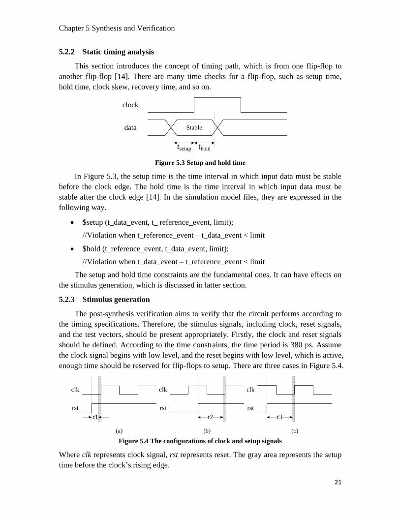
This section introduces the concept of timing path, which is from one flip-flop to
another flip-flop [14]. There are many time checks for a flip-flop, such as setup time,
hold time, clock skew, recovery time, and so on.
tsetup thold
Stable
clock
data
Figure 5.3 Setup and hold time
In Figure 5.3, the setup time is the time interval in which input data must be stable
before the clock edge. The hold time is the time interval in which input data must be
stable after the clock edge [14]. In the simulation model files, they are expressed in the
following way.
$setup (t_data_event, t_ reference_event, limit);
//Violation when t_reference_event – t_data_event < limit
$hold (t_reference_event, t_data_event, limit);
//Violation when t_data_event – t_reference_event < limit
The setup and hold time constraints are the fundamental ones. It can have effects on
the stimulus generation, which is discussed in latter section.
5.2.3 Stimulus generation
The post-synthesis verification aims to verify that the circuit performs according to
the timing specifications. Therefore, the stimulus signals, including clock, reset signals,
and the test vectors, should be present appropriately. Firstly, the clock and reset signals
should be defined. According to the time constraints, the time period is 380 ps. Assume
the clock signal begins with low level, and the reset begins with low level, which is active,
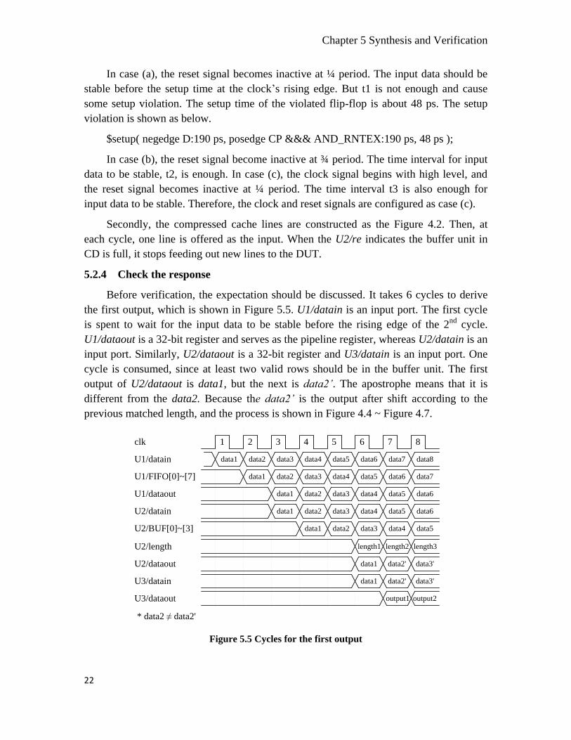
enough time should be reserved for flip-flops to setup. There are three cases in Figure 5.4.
clk
rst
clk
rst
clk
rst
t2 t3t1
(a) (b) (c)
Figure 5.4 The configurations of clock and setup signals
Where clk represents clock signal, rst represents reset. The gray area represents the setup
time before the clock‟s rising edge.
Chapter 5 Synthesis and Verification
22
In case (a), the reset signal becomes inactive at ¼ period. The input data should be
stable before the setup time at the clock‟s rising edge. But t1 is not enough and cause
some setup violation. The setup time of the violated flip-flop is about 48 ps. The setup
violation is shown as below.
$setup( negedge D:190 ps, posedge CP &&& AND_RNTEX:190 ps, 48 ps );
In case (b), the reset signal become inactive at ¾ period. The time interval for input
data to be stable, t2, is enough. In case (c), the clock signal begins with high level, and
the reset signal becomes inactive at ¼ period. The time interval t3 is also enough for
input data to be stable. Therefore, the clock and reset signals are configured as case (c).
Secondly, the compressed cache lines are constructed as the Figure 4.2. Then, at
each cycle, one line is offered as the input. When the U2/re indicates the buffer unit in
CD is full, it stops feeding out new lines to the DUT.
5.2.4 Check the response
Before verification, the expectation should be discussed. It takes 6 cycles to derive
the first output, which is shown in Figure 5.5. U1/datain is an input port. The first cycle
is spent to wait for the input data to be stable before the rising edge of the 2nd
cycle.
U1/dataout is a 32-bit register and serves as the pipeline register, whereas U2/datain is an
input port. Similarly, U2/dataout is a 32-bit register and U3/datain is an input port. One
cycle is consumed, since at least two valid rows should be in the buffer unit. The first
output of U2/dataout is data1, but the next is data2’. The apostrophe means that it is
different from the data2. Because the data2’ is the output after shift according to the
previous matched length, and the process is shown in Figure 4.4 ~ Figure 4.7.
data1 data2 data3 data4 data5 data6 data7
clk
U1/datain
U1/FIFO[0]~[7] data2 data3 data4 data5 data6 data7data1
U1/dataout
U2/datain
U2/BUF[0]~[3]
data1
1 2 3 4 5 6 7 8
data8
U2/dataout
U3/datain
U3/dataout
data2 data3 data4 data5 data6
data1 data2 data3 data4 data5 data6
data1 data2 data3 data4 data5
data1 data2'
output1
data1
output2
data2'
data3'
data3'
U2/length length1 length2 length3
* data2 ≠ data2'
Figure 5.5 Cycles for the first output

Chapter 5 Synthesis and Verification
23
The specific operations for each cycle are explained in Table 5.1. After the first
output, it generated one uncompressed value for each cycle. It takes 22 cycles to
decompress the first compressed cache block.
Table 5.1 Operations for the first output
Cycles Operations
1 Input compressed data is available and stable at U1/datain, i.e. data1.
2 Data1 is stored in the first row of U1/FIFO, i.e. U1/FIFO[0].
3 Data1 is read from the U1/FIFO[0], and present at U1/dataout and U2/datain..
4 Data1 is stored in the first row of U2/BUF, i.e. U2/BUF[0].
5 Data2 is stored in the second row of U2/BUF. i.e. U2/BUF[1].
6 Matched length and data1 are present at U2/dataout and U3/datain.
7 The value is retrieved from DeLUT and present at U3/dataout.
Figure 5.6 and Figure 5.7 show the verification waveforms from the beginning to
21st cycle. It takes 7 cycles to produce the first decoded value. It is 0. At that moment, the
sig_validre becomes „1‟ to indicate the validity of output. Since then, there is one
decompressed value in each cycle. At each cycle the output data is compared with the
original value. If there is a difference, a warning will be alerted.
Figure 5.6 Verification waveform from 1st to 11
th cycle
Figure 5.7 Verification waveform from 11th
to 21st cycle

Chapter 5 Synthesis and Verification
24
5.2.5 Configuration of the FIFO
As mentioned before, in order to avoid buffer starvation, a FIFO structure with 4
registers is suitable. The total sizes of the FIFO stage and buffer unit are 12 rows.
According to Figure 5.5, if the decompression engine does not work, the 12 rows should
be full at the 13th
cycle. However, the decompression engine begins to decompress after
the 6th
cycle. At the 13th
cycle, it will already have decoded 7 values, while the rest 9
compressed CWs are stored in the FIFO stage and the buffer unit. In the worst case, the 9
values can be uncompressed requiring 32 bits plus unique code. It was experimentally
found that the unique code never exceeds 9 bits (41 bits per uncompressed value), while
the analysis of the thesis assumes 4 bits for it, as the generated unique code has always a
length of 4 for the benchmark omnetpp. Therefore, 12 rows are enough to hold one
compressed cache block. However, if the unique code is as long as the longest CWs, i.e.,
16 bits, 2 more FIFO rows (10 rows in total) are required in the FIFO stage. The two
extra FIFO rows extend the delay of the FIFO stage by approximately 5ps, without
affecting the overall performance, as the critical paths are in CD and VR stages.
Sometimes, a series of uncompressed values appear consecutively. In such cases, the
number of bits consumed per cycle is more than 32 bits due to the unique code that
precedes an uncompressed value. This could cause a 1-cycle wait in the decompression
process, as the buffer unit must have at least two valid rows.
5.3 Summary
(1) The implementation is successfully verified under 380 ps.
(2) The library used to synthesize the implementation is 1.30V, -40℃.
(3) The first decoded value is available at the 7th
cycle.
(4) When a series of uncompressed values occur consecutively, it could cause a 1-cycle
wait in the decompression process.

25
6 Performance and Power Evaluation
This chapter firstly introduces the background knowledge of performance and power
analysis for VLSI design. Then, it evaluates the decompressor in terms of performance
and power dissipation/energy consumption varying the voltage thresholds, the
environment temperature as well as the DeLUT size.
6.1 Performance
6.1.1 Static timing analysis
After synthesis, an actual cycle time has to be met by a particular set of gates. A
timing analyzer is used to verify the timing [16]. Static timing analysis is a method to
verify the timing of a design by testing all possible paths for timing violations. It
considers the worst possible delay, but not the logical validity of the circuit [14].
Each path in the design has a timing slack, which is the result of data arrived time
subtract from data required time. It is a time value that can be positive, zero, or negative.
The positive value means the signal arrives earlier than necessary and the timing
constraint is met, where the zero slack means the timing constraint is barely fulfilled, and
the timing constraint is violated for negative slack. The path having the worst slack,
which means the longest latency, is called the critical path.
6.1.2 Critical paths
After static timing analysis, the critical paths are generated in a timing report. In my
design, there are two critical paths exist in CD and VR, respectively. In the CD stage, the
path from the read address of buffer unit (U2/radd[0]) to itself (U2/radd[0]) is the most
time consuming, whereas the path from the input length (U3/length[4]) to the output data
(U3/dataout_reg[12]) takes the longest time in VR stage.
The critical path in the CD stage indicates the logic for read address controller is
very complicated. The modification of the read address is triggered by clock rising edge,
so U2/radd[0] is synthesized to be a register. The read address depends on the matched
length of the previous cycle. After read, a new data row is produced by the barrel shifter
for the unique code detection and comparison. The detected and/or compared results are
used for next cycle. So the path for the read address control includes both the unique code
detection and comparison circuits. Besides, the comparison circuit is implemented with
priorities in a synchronized process. In the worst case, for a 16-bit compressed codeword,
it should execute 16 times comparison operations, hence increasing the path length.

Chapter 6 Performance and Power Analysis
26
In the VR stage, the input matched length is synchronized. After a subtraction and a
look-up operation, the decompressed value is available on the output port. So the critical
path in VR stage means the read speed of ROM is very slow.
6.1.3 Design Variation
There are two major design variations in the thesis, supply voltage and environment
temperature. Simply, the delay of a transistor can be defined as [16]
2
DD DSAT DD DD t/ / ( )t C V I k C V V V (6.1)
where, C is the load capacitance, VDD is the supply voltage, IDSAT is saturation current, k is
the gain factor, Vt is the threshold voltage. So the frequency is proportional to the supply
voltage. At the same voltage, frequency is proportional to the saturation current, which
can be influenced by temperature.
Temperature can affect transistor characteristics very much. With the increase of
temperature, Carrier mobility drops and may be approximated by [16]
μ( ) μ( )
k
r
r
TT T
T
(6.2)
where T is the absolute temperature, Tr is room temperature, and k is a fitting parameter
with a typical value of 1.5.
Besides, with the increase of temperature, the magnitude of the threshold voltage
decreases nearly linearly. An approximate relation is
( ) ( ) ( )t t r vt rV T V T k T T (6.3)
where a typical value of kvt is about 1-2 mV/K.
To conclude the temperature effects, with the increase of temperature, the saturation
current decreases, but the junction leakage increases exponentially [16]. Therefore, as the
environment temperature increases, the circuit‟s operational frequency drops and the
static power increase exponentially. The effects of temperature on power consumption
will be discussed in next section. By running a large number of experiments, the
maximum delay of each design variation for the synthesized circuits, which is also called
period, is shown in Table 6.1, where NA means the library (1.30V, 0℃) does not exist.
Table 6.1 Period of each design variation (Unit ps)
1.30V 1.15V 1.10V
-40℃ 380 444 467
0℃ NA 451 472
125℃ 399 465 477

Chapter 6 Performance and Power Analysis
27
In the power analysis described below, the VR stage is most power hungry. The
main task in VR stage is the looking-up operation to retrieve the value in DeLUT, so the
size of DeLUT may influence the performance and power. Further analysis of
performance and power with different sizes of DeLUT is elaborated in section 6.2.5.
6.2 Power Analysis
6.2.1 Power definition
Power consumption in CMOS circuits comes from two components, dynamic and
static consumption [16].
dynamic staticP P P (6.4)
Dynamic power consists of switching power and internal power. The switching
power is caused by charging load capacitance. The internal power is caused by charging
internal capacitance and short circuits.
load
2sw swDDP C V f (6.5)
21
2int int DD sw DD scP C V f V I (6.6)
Where is the activity factor indicating the probability that circuit node transitions from
0 to 1, Cload is the load capacitance, Cint is the internal capacitance, VDD is the supply
voltage, fsw is the switching frequency, Isc is the short circuit current.
Static power is caused when a transistor is not switching. It comes from
subthreshold, gate, and junction leakage currents [16]. In nanometer processes with low
threshold voltages and thin gate oxides, leakage power is comparable to dynamic power.
In some cases, it may even dominate the overall power consumption.
There are two ways for switching power analysis, simulation-based techniques and
probabilistic techniques [17]. In simulation-based power analysis, input test vectors
should be prepared. The idea behind the probabilistic technique is to derive switching
probabilities of all internal nodes by propagating the input signal switching activities. It is
just used in early development phases, when test vectors are not available. The designer
must understand the functionality deeply to predict the input signal probability. Since I
have already obtained the test vectors in previous chapters, the simulation-based
techniques will be used.
There are two ways to perform the statistical analysis. Either a value change dump
(VCD) or a switching activity interchange file (SAIF) file is generated. A VCD file
contains information of all signals that toggle, for every clock cycle. As a result, VCD
files can grow huge. In contrast, the SAIF file contains only the average switching
activity of all nodes.

Chapter 6 Performance and Power Analysis
28
6.2.2 Test vectors setup
Two power models are used to estimate the power:
(1) Real case, where a cache snapshot, with 16384 compressed cache blocks, is obtained
using architectural simulation of a system running particular benchmarks. The
modeled cache is a last-level cache (L3).
(2) Corner cases, cache blocks are built artificially to estimate power dissipation, which
may not appear in the cache snapshot. Table 6.2 summarizes all the test cases.
Table 6.2 Cache block cases used in power estimation
Cases Construction
1 Real cases from snapshot
2 12 uncompressed + 4 compressed (16-bit)
3 14 uncompressed + 2 compressed (1-bit)
4 8 uncompressed + 8 compressed(1-bit)
5 16 compressed (16-bit)
6 16 compressed (1-bit)
7 compressed CW with evenly distributed length
Case 1 is the real case, so the power dissipation should approximate a real value.
Cases 2 and 3 are lines that are compressed by a relatively small compression factor.
Their lengths are 496 bits and 506 bits respectively, while an original cache block has
512 bits but is not needed to be decompressed. Case 4 is a similar combination, but with
more values that are compressed by the highest factor (32/1). In case 5, the values are
compressed by a compression factor of 32/16 while in case 6, they are all compressed by
a factor of 32/1. Finally, case 7 has compressed CWs with evenly distributed length,
close to the real case.
The power analysis begins with post synthesis verification, where the switching
activity of the decompressor circuit is recorded in a VCD file. In the experiment of this
study, the VCD contains the circuit‟s switching activity for 1607 cycles, while
decompressing 100 cache blocks, where the cycle 380 ps.
6.2.3 Power analysis based real and corner cases
After a series of experiments, their power consumptions (in mW) are listed in Table
6.2. Since the library “1.30V, -40℃” is used, the static power dissipation of all cases are
kept in low levels.
Chapter 6 Performance and Power Analysis
29
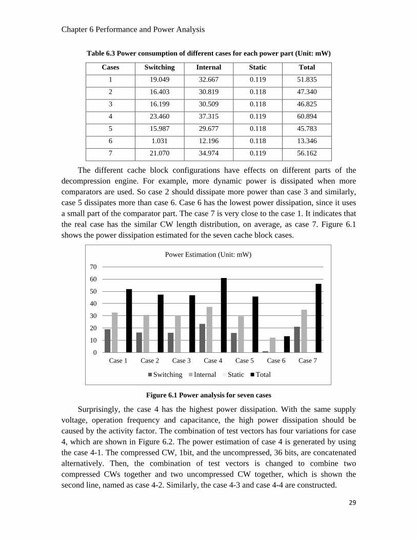
Table 6.3 Power consumption of different cases for each power part (Unit: mW)
Cases Switching Internal Static Total
1 19.049 32.667 0.119 51.835
2 16.403 30.819 0.118 47.340
3 16.199 30.509 0.118 46.825
4 23.460 37.315 0.119 60.894
5 15.987 29.677 0.118 45.783
6 1.031 12.196 0.118 13.346
7 21.070 34.974 0.119 56.162
The different cache block configurations have effects on different parts of the
decompression engine. For example, more dynamic power is dissipated when more
comparators are used. So case 2 should dissipate more power than case 3 and similarly,
case 5 dissipates more than case 6. Case 6 has the lowest power dissipation, since it uses
a small part of the comparator part. The case 7 is very close to the case 1. It indicates that
the real case has the similar CW length distribution, on average, as case 7. Figure 6.1
shows the power dissipation estimated for the seven cache block cases.
Figure 6.1 Power analysis for seven cases
Surprisingly, the case 4 has the highest power dissipation. With the same supply
voltage, operation frequency and capacitance, the high power dissipation should be
caused by the activity factor. The combination of test vectors has four variations for case
4, which are shown in Figure 6.2. The power estimation of case 4 is generated by using
the case 4-1. The compressed CW, 1bit, and the uncompressed, 36 bits, are concatenated
alternatively. Then, the combination of test vectors is changed to combine two
compressed CWs together and two uncompressed CW together, which is shown the
second line, named as case 4-2. Similarly, the case 4-3 and case 4-4 are constructed.
0
10
20
30
40
50
60
70
Case 1 Case 2 Case 3 Case 4 Case 5 Case 6 Case 7
Power Estimation (Unit: mW)
Switching Internal Static Total

Chapter 6 Performance and Power Analysis
30
1bit + 36bits +1bit + 36bits + 1bit + 36bits +……
1bit + 1bit + 36bits + 36bits +1bit + 1bit + ……
1bit + … + 1bit + 36bits + …… + 36bits +1bit +...
1bit + … + 1bit + 36bits + …… + 36bits
1
2
1
2
4 4
8 8
case 4-1
case 4-2
case 4-3
case 4-4
Figure 6.2 The different structure of test vectors
After analysis, their power dissipations are shown in Table 6.4. Since the case 4-1
always alternates between compressed and uncompressed CW, it increases the switching
probability and the glitch in the circuits, thus largely increasing the switching power. The
case 4-4 only alternates once per compressed cache block, so it consumes least power.
From case 4-1 to case 4-4, the dynamic power consumptions decrease gradually. Because
in case 2 and case 3 the alternation between compressed and uncompressed parts occur
once per cache block, case 4-4 is more representative therefore it is used in the following
comparisons.
Table 6.4 Power dissipation for different test vector structures (Unit: mW)
Switching Internal Static Total
Case 4-1 23.460 37.315 0.119 60.894
Case 4-2 20.298 34.051 0.118 54.468
Case 4-3 17.305 30.993 0.118 48.416
Case 4-4 15.408 29.017 0.118 44.543
6.2.4 Power distribution among three stages
In the previous analysis, the power distributions among three kinds of power are
described. It makes clear how the switching activity depends on the different cases, and
the combinations of test vectors. Another interesting topic is how the power consumption
is distributed among the three stages. From this analysis, the further optimization on
power is more accurately targeted. shows power consumption for each stage.
The power consumption of the FIFO is very stable, and it fluctuates between 6.520
mW to 9.110 mW. In the case 6, all of the compressed CW is „0‟, which uses only 1 bit in
the FIFO buffer row. 32 bits „0‟ constitute one FIFO buffer row which represent 32
values 010. Therefore, only one buffer row is read from the FIFO in the decompression of
each cache block, hence decrease the power dissipation. The case2 and case3 have the
comparatively low compression factor, so the read frequency of them is higher than other
cases, which cause the high power dissipation in FIFO stage.

Chapter 6 Performance and Power Analysis
31
Table 6.5 Power dissipation of different cases in each stage (Unit: mW)
Cases FIFO CD VR Total
1 8.015 11.051 32.769 51.835
2 9.110 11.630 26.600 47.340
3 8.935 11.282 26.608 46.825
4-4 7.979 10.913 25.654 44.543
5 8.359 10.859 26.565 45.783
6 6.520 5.769 1.056 13.346
7 8.352 12.226 35.585 56.162
In the CD stage, the power dissipation is also stable, except for the case 6. In the
comparator of the CD stage, there is a priority encoder and the length 1 has the highest
priority. In the case 6, all compressed CWs are „0‟s with length 1. So it uses the least
power. Other cases show that the normal range of the power dissipation in the CD stage
is from 10.913 mW to 12.226 mW.
The VR stage is the most power consuming. The major parts in the VR stage are two
LUTs, i.e. DIT, DeLUT, and a multiplex. A LUT is implemented by a couple of
multiplexers and a 2-input multiplexer consists of four transistors. The DIT is a 5-
inputand the DeLUT is a 10-input multiplexer. So the power dissipated in looking-up
operation dominates. According to the definition of dynamic power, the less switch
activity, the less power dissipation. The value 010 is located at the beginning of the
DeLUT. In the case 6, the value it looked up is fixed, so it contains the least switch
activity and least power dissipation. In the case 7, the compressed CWs are evenly
distributed, the switch activity is the highest hence the highest power dissipation. In the
case 1, there are some uncompressed values, so the power dissipation is lower than case 7.
According to the power analysis above, the VR stage should be optimized for power.
6.2.5 Power consumption for different DeLUT sizes
Since the VR stage is the power hungry, it is interesting to investigate how the
performance and power dissipation depends on the DeLUT size. As mentioned before,
the DeLUT is 4KB in the thesis, which is the baseline in this section‟s analysis. In order
to maintain the generality, the power consumptions with different VFT sizes, in other
words, different DeLUT sizes are shown in Table 6.6. The performance is represented by
the period the circuits can achieve, which is the reciprocal of the frequency. With the
increase of the DeLUT size the performance degrades, power dissipation and area
consumption increase.

Chapter 6 Performance and Power Analysis
32
Table 6.6 Performance, power and area varying with DeLUT size
1KB 2KB 4KB 8KB 16KB
Time (ps) 358 367 380 395 413
Power (mW) 44.821 46.578 51.835 84.932 118.511
Area (cell) 7807 8324 9223 14666 20955
6.2.6 Design variation
The effects of supply voltage and environment temperature have been analyzed in
section 6.1.3. By running the same testbench, with corresponding period, the power
consumption of each library are obtained and listed in Table 6.7
Table 6.7 Power consumptions of each design variation (Unit mW)
1.30V 1.15V 1.10V
-40℃
Switch Internal Static Switch Internal Static Switch Internal Static
19.049 32.667 0.119 11.921 20.186 0.056 10.746 17.856 0.046
51.835 32.162 28.648
0℃
Switch Internal Static Switch Internal Static Switch Internal Static
NA NA NA 12.306 21.178 0.336 11.311 18.504 0.296
NA 33.820 30.111
125℃
Switch Internal Static Switch Internal Static Switch Internal Static
18.476 36.101 11.898 11.942 23.625 6.921 10.523 20.914 6.760
66.475 42.488 38.198
The dynamic power, including the switching and internal power, mainly relies on
the supply voltage. On the other side, the static power is strongly dependent the
environment temperature. With the same temperature, the static power of each design
variation is in the same magnitude level. The high supply voltage, 1.30V, can increase the
static power for the same temperature.
6.3 Energy Analysis
In the VLSI design, the trade-off between performance and power is an important
consideration. If a library with lower voltage threshold, such as the (1.10V, -40℃), is
used to synthesize the implementation, the maximum frequency can be reached should be
lower. Besides, the power will be lower due to the lower supply voltage. The energy
consumed to decompress the certain quantity of cache blocks is used to assess the energy
efficiency. By using the results in Table 6.1 and Table 6.7, the energy consumption to
decompress one cache block is calculated in the corresponding position in Table 6.8 and
shown in Figure 6.3. The library of 1.10V and -40℃ has the lowest energy consumption
to derive one decompressed cache block.
DeLUT

Chapter 6 Performance and Power Analysis
33
Table 6.8 Energy of each design variation (Unit J)
1.30V 1.15V 1.10V
-40℃ 315.2 228.5 214.1
0℃ NA 244.0 235.0
125℃ 424.4 316.1 291.5
Figure 6.3 Energy of each design variation to decompress one cache block
6.4 Summary
(1) The power consumption includes dynamic power and static power.
(2) For the same circuit, it is the switch activity that affects the dynamic power, hence the
power consumption. The power estimation indicates that the real case has evenly
distributed CW length with uncompressed values
(3) The dynamic power mainly depends on the switch activity and supply voltage. The
different test vectors, even the different combinations of test vectors can have effects
on the dynamic power.
(4) The static power mainly depends on the environment temperature. Besides, the
increase of supply voltage can increase the static power a little for the same
temperature.
(5) The circuit frequency is proportional to the supply voltage. At the same voltage,
frequency is proportional to the saturation current, which can be influenced by
temperature.
(6) The library of 1.10V and -40℃ has the lowest energy consumption to derive one
decompressed cache block.
0
50
100
150
200
250
300
350
400
450
1.30V 1.15V 1.10V
Energy of each design variation
(Unit: pJ)
-40 C 0 C 125 C

Chapter 6 Performance and Power Analysis
34

35
7 Conclusion
In order to make full use of the smaller cache and therefore saving the consumed
power, a Huffman-based decompression engine is proposed by Arelakis and Stenström.
The thesis describes a detailed design and implementation of the decompression engine.
After design and implementation, the decompression engine has been synthesized and
verified and it fulfills the specifications. Finally, the power consumption of the engine
has been analyzed.
The decompression engine is implemented in a 3-stage pipeline structure, which
comprises FIFO buffer, Code Detection (CD) and Value Retrieve (VR). It takes 6 cycles
to obtain the first decompressed value. After that, it can derive one 32-bit uncompressed
value per cycle. It is successfully synthesized when the time constraint is 380 ps. In the
power analysis, firstly, 7 different cases, i.e. sets of test vectors, are used. Even in one
case, i.e. the case 4, which contains 8 uncompressed value and 8 compressed CWs with
length of 1-bit, the power consumption of 4 different test vectors‟ combinations are
compared. In this part, it is the switch activity that affects the dynamic power, hence the
power consumption. Secondly, by using the real case as the test vectors, the power
consumptions of different design variations are compared to investigate the influence of
the supply voltage and environment temperature.
The design is synthesized by the best library, 1.30 V and -40℃, of 28 nm process
technology. However, it should be synthesized and verified by using the worst library
before manufacture. Performance can be further improved in the future, taking into
consideration the following observations: firstly, the delay of the Code detection stage
can be improved, adjusting the sequential logic and combinational logic proportion to
make use of the parallelism. Secondly, more standard components in DesignWare IP
solutions provided by Synopsys should be inferred to reuse these optimized components.
Thirdly, the DIT and DeLUT in VR stage should be implemented by static RAM instead
of ROM to improve the performance further. Fourthly, the place and route should be
achieved to increase the accuracy of the timing.
In conclusion, the timing and power analyses of the implementation of this
Huffman-based decompressor have shown that the design can be clocked at 2.63 GHz
and dissipates maximum 51.835 mW, on average, while further enhancements are
possible. This thesis shows that the design of this Huffman decompressor is a strong
candidate among other decompression mechanisms targeting to statistical-based

Chapter 7 Conclusion
36
compressed cache/memories, thanks to its design simplicity and high efficiency in terms
of performance and power.

37
Bibliography
[1] John L. Hennessy, David A. Patterson. “Memory Hierarchy Design”, Computer
Architecture -- A quantitative approach, Morgan Kaufmann, 2011, pp.74.
[2] Alameldeen, A.R.; Wood, D.A., "Adaptive cache compression for high-
performance processors," Computer Architecture, 2004. Proceedings. 31st Annual
International Symposium on , vol., no., pp.212,223, 19-23 June 2004
[3] Xi Chen; Lei Yang; Dick, R.P.; Li Shang; Lekatsas, H., "C-Pack: A High-
Performance Microprocessor Cache Compression Algorithm," Very Large Scale
Integration (VLSI) Systems, IEEE Transactions on , vol.18, no.8, pp.1196,1208,
Aug. 2010
[4] A. Arelakis and P. Stenström, “A Case for a Value-Aware Cache”, IEEE Computer
Architecture Letters, September 2012.
[5] A. Arelakis, “Design Considerations of Value-aware Cache”, Licentiate degree
thesis, September 2013.
[6] Stefan M. Moser. “Shannon‟s Measure of Information”, Information Theory,
Lecture Notes. pp 6.
[7] Salomon, D. “Huffman Coding”, A concise introduction to Data compression,
Springer 2008,pp 63~64,75.
[8] L. Stok, D. Hathaway, K. Keutzer, D. Chinnery. “Design Flows”, EDA for IC
Implementation Circuit Design and Process Technology, CRC Press Taylor &
Francis Group, New York, 2006,pp. 1-1~3.
[9] R. Hashemian, “Design and hardware implementation of memory efficient
Huffman decoding,” IEEE Trans. Consumer Electron., vol. 40, pp. 345-352,
Aug.1994.
[10] S. M. Lei and M. T. Sun, “An Entropy Coding System for Digital HDTV
Applications,” IEEE Trans. Circuits and System For Video Technology, vol.1,
No.1, pp147-155, March.1991.
[11] J. Nikara, S. Vassiliadis, J. Takala and P. Liuha. ”Multiple-Symbol Parallel
Decoding for Variable Length Codes,” IEEE Trans. Very Large Scale Integration
(VLSI) Systems, vol.12, No.7, pp676-685, July 2004.
[12] Synopsys, Design Compiler User Guide, Ver. D-2010.03-SP2, June 2010

Bibliography
38
[13] C. Spear, SystemVerilog for Verification, A guide to learning the testbench
language features Springer, 2006
[14] Synopsys, Timing Constraints and Optimization User Guide, Ver. F-2011.09. Sept.
2011
[15] M. Arora, The Art of Hardware, Design Methods and Techniques for Digital
Circuits. 2011
[16] N. H.E. Weste, D. M. Harris, Integrated circuit design, 4th edition, Pearson,
2011,pp. 85, 142~143, 598.
[17] J. Monteiro, R. Patel, V. Tiwari. “Power Analysis and Optimization from Circuit to
Register-Transfer Levels”, EDA for IC Implementation Circuit Design and Process
Technology, CRC Press Taylor & Francis Group, New York, 2006,pp. 3-6~8.