design and development of an embedded homeplug green𝑃 web
TRANSCRIPT

Design and Development of an Embedded HomePlug
Green𝑃𝐻𝑌𝑇𝑀 Web Based System for Demand Side Management in
Smart Home Applications
By
Adeola Azeez Ogunleye
March 2016
Faculty of Engineering
Department of Electrical and Electronic Engineering
Supervisors: Dr PJ. Randewijk and Dr Riaan Wolhuter
Thesis presented in partial fulfilment of the requirements for the degree
Master of Science in Engineering
at Stellenbosch University

i
DECLARATION
By submitting this thesis electronically, I declare that the entirety of the work contained
therein is my own original work, that I am the sole author thereof (save to the extent
explicitly otherwise stated), that reproduction and publication thereof by Stellenbosch
University will not infringe any third party rights and that I have not previously in its entirety
or in part submitted it for obtaining any qualification.
Date: March 2016
Copyright © 2016 Stellenbosch University
All rights reserved
Stellenbosch University https://scholar.sun.ac.za

ii
ABSTRACT
This thesis provides an overview of the design of a web-based Power Line Communication
(PLC) interface. The communication system is a combination of various units such as a
webpage, a webserver, a power line communication module and a Relay and Power
Measuring Unit (RPMU). The aim of design is to encourage consumers to participate in a
Demand Side Management (DSM) since their home appliances can be controlled remotely.
Technological advancement are encouraging us to have smarter homes, offices and even cars
that reduce demand for energy derived from coal, gas or other energy substances causing
global warming. Necessary hardware was designed and the embedded software was
implemented. A communication protocol was created for data communication between the
HomePlug GreenPHY𝑇𝑀 nodes. The testing of the project was adequately documented in this
thesis. This project demonstrates a practical application of Internet of Things (IoT) due to the
fact that Internet is now ubiquitous and affordable.
Stellenbosch University https://scholar.sun.ac.za

iii
UITTREKSEL
.
Hierdie tesis bespreek die ontwerp van ‟n webgebaseerde kommunikasiekoppelvlak vir
kraglyne. Die kommunikasiestelsel bestaan uit verskeie eenhede soos ‟n webblad,
webbediener, Home plug greenPHY (HPGP) en ‟n relê en kragmeeteenheid (RPMU). Die
ontwerp moedig verbruikers aan om deel te hê aan die beheer van die vraag na krag,
aangesien die toestelle in die huis vanaf ‟n afstand beheer kan word. Tegnologiese
vooruitgang moedig ons aan om slimmer huise, kantore en motors te besit. Dit verminder die
vraag na krag wat afkomstig is van steenkool, gas en ander stowwe wat kweekhuisgasse
veroorsaak. Die ontwerp en implementering van die sagteware vir die toegewyde stelsel en
meegaande hardeware word bespreek. ‟n Kommunikasieprotokol is geskep vir die versending
van data tussen HPGP-eenhede. Toetspresedures en resultate is gedokumenteer. Die stelsel
verteenwoordig 'n praktiese en nuttige toepassing van die “Internet of Things”, aangesien die
Internet oral en goedkoop ingespan kan word.
Stellenbosch University https://scholar.sun.ac.za

iv
ACKNOWLEDGEMENTS
I want to specially thank God for making this day come to pass. He is most beneficent and
the most merciful.
I want to thank my parents, Mr and Mrs Ogunleye for the financial and moral support when I
faced adversity. Special thanks are due to my sister Ogunleye Alimot Adenike.
I want to thank my supervisors Dr PJ Randewijk and Dr Wolhuter for their guidance.
I want to thank Centre for Renewable and Sustainable Energy for the financial support.
Special thanks are due to Christianah Oyindamola Olojede for her tremendous support and
effort during the editing of the thesis.
I am also grateful to my friends Criag Omotoyosi, Odukoya Oluseye and Oladele Temitope.
I want to appreciate Mr. J. Arendse for soldering the PCB.
I am also grateful to Mr A.Barnard for his time and useful advice.
I want to thank Brother Muhammad Junaid for his assistance during my program.
Stellenbosch University https://scholar.sun.ac.za

v
TABLE OF CONTENTS
ABSTRACT ........................................................................................................................................... II
UITTREKSEL ...................................................................................................................................... III
ACKNOWLEDGEMENTS .................................................................................................................. IV
LIST OF FIGURES .............................................................................................................................. XI
LIST OF TABLES ............................................................................................................................. XIV
PUBLICATION .................................................................................................................................. XV
LIST OF ABBREVIATIONS ............................................................................................................ XVI
1 INTRODUCTION ........................................................................................................................ 1
1.1 OVERVIEW ................................................................................................................................. 1
1.2 PROBLEM STATEMENT ........................................................................................................... 1
1.3 PROJECT MOTIVATION ........................................................................................................... 2
1.4 AIM .............................................................................................................................................. 2
1.5 PROJECT DESCRIPTION .......................................................................................................... 2
1.6 TECHNICAL APPROACH ......................................................................................................... 3
1.7 REQUIRED SKILLS AND RESOURCES .................................................................................. 4
1.8 IMPORTANCE OF THE PROJECT ............................................................................................ 4
1.9 THESIS OUTLINE ...................................................................................................................... 5
2 LITERATURE REVIEW ............................................................................................................. 6
2.1 POWER LINE COMMUNICATION .......................................................................................... 6
2.2 BRIEF HISTORY OF POWER LINE COMMUNICATION ...................................................... 7
2.3 HOMEPLUG POWER LINE ALLIANCE .................................................................................. 7
2.4 HOMEPLUG VERSIONS AND USES ....................................................................................... 8
2.4.1 HOMEPLUG 1.0 ................................................................................................................... 8
2.4.2 HOMEPLUG GREENPHY𝑇𝑀 (HPGP) ................................................................................ 8
2.4.3 HOMEPLUG ACCESS BPL................................................................................................. 8
Stellenbosch University https://scholar.sun.ac.za

vi
2.4.4 HOMEPLUG AV .................................................................................................................. 9
2.4.5 HOMEPLUG AV2 ................................................................................................................ 9
2.4.6 OTHER POWERLINE MODULES ................................................................................... 10
2.4.6.1 G3-PLC ........................................................................................................................ 10
2.4.6.2 PRIME ......................................................................................................................... 10
2.5 PLC COMPARED TO WIRELESS SMART GRID TECHNOLOGIES .................................. 10
2.6 CLASSIFICATION OF POWER LINE COMMUNICATION NETWORK ............................ 10
2.7 HOME-CONTROL NARROW BAND ..................................................................................... 11
2.8 LOW-SPEED NARROW BAND ............................................................................................... 11
2.9 MEDIUM-SPEED NARROW BAND ....................................................................................... 11
2.10 BROAD-BAND ....................................................................................................................... 12
2.11 PLC MODULATION .............................................................................................................. 12
2.11.1 SINGLE–CARRIER MODULATION .............................................................................. 12
2.12 HOME PLUG GREENPHY‟S MODULATING TECHNIQUE (QPSK) ............................... 13
2.13 SPREAD-SPECTRUM MODULATION ................................................................................ 14
2.14 ORTHOGONAL FREQUENCY DIVISION MULTIPLEXING (OFDM) ............................ 15
2.15 COMMUNICATION STRATEGY ON THE MEDIUM ........................................................ 15
2.15.1 TOKEN PASSING ............................................................................................................ 16
2.15.2 CONTENTION .................................................................................................................. 16
2.15.3 POLLING .......................................................................................................................... 16
2.15.4 ALOHA ............................................................................................................................. 16
2.16 SMART GRID NETWORK .................................................................................................... 16
2.16.1 HOME AREA NETWORK (HAN) ................................................................................... 17
2.16.2 WIDE AREA NETWORK (WAN) ................................................................................... 17
2.16.3 NEIGHBOURHOOD AREA NETWORK (NAN) ........................................................... 18
2.17 NOISE HARMONICS IN A POWER LINE COMMUNICATION NETWORK .................. 18
2.17.1 SINGLE-EVENT IMPULSE NOISE ................................................................................ 19
Stellenbosch University https://scholar.sun.ac.za

vii
2.17.2 NOISE HAVING LINE COMPONENTS SYNCHRONOUS WITH POWER SYSTEM
FREQUENCY ................................................................................................................................. 19
2.17.3 A SMOOTH SPECTRUM NOISE .................................................................................... 19
2.17.4 NON-SYNCHRONOUS NOISE ....................................................................................... 20
2.18 ATTENUATION ON POWER LINE SYSTEM ..................................................................... 20
2.19 IMPEDANCE OF POWER LINE SYSTEM .......................................................................... 21
2.20 SIGNAL-TO-NOISE RATIO (SNR) ...................................................................................... 24
2.21 SUMMARY ............................................................................................................................. 24
3 HARDWARE DESIGN.............................................................................................................. 25
3.1 DESIGNING THE SYSTEM ..................................................................................................... 25
3.2 CS5490 ....................................................................................................................................... 26
3.2.1 SHUNT CALCULATION FOR THE CS5490 ................................................................... 28
3.2.2 VOLTAGE SENSING ........................................................................................................ 28
3.3 POWER SUPPLY UNIT ............................................................................................................ 30
3.4 LOAD SWITCHING WITH A RELAY .................................................................................... 31
3.5 ISOLATION ............................................................................................................................... 31
3.6 MOSFET AS A SWITCH .......................................................................................................... 32
3.7 FUSE .......................................................................................................................................... 33
3.8 CRYSTAL OSCILLATOR ........................................................................................................ 33
3.9 CONNECTOR AND PINHEADS ............................................................................................. 34
3.10 BEAGLEBONE BLACK ........................................................................................................ 34
3.10.1 UARTS ON THE BEAGLEBONE BLACK ..................................................................... 36
3.11 HOMEPLUG GREENPHY𝑇𝑀 (HPGP) MODULE ................................................................ 36
3.11.1 INTERFACING WITH THE HPGP MODULE ............................................................... 38
3.11.2 UART ON THE MK20DX256VMC7 ............................................................................... 39
3.11.2.1 UART SETTINGS ON THE MK20DX256VMC7 ................................................... 39
3.11.2.2 WORKING UART OF MK20DX256VMC7 ............................................................ 40
3.12 RELAY AND POWER MEASURING UNIT (RPMU) ......................................................... 41
Stellenbosch University https://scholar.sun.ac.za

viii
3.13 PCB DESIGN .......................................................................................................................... 41
3.14 SUMMARY ............................................................................................................................. 42
4 EMBEDDED SOFTWARE ........................................................................................................ 43
4.1 THE MAIN PROGRAM ON THE BEAGLEBONE BLACK................................................... 43
4.2 RTOS .......................................................................................................................................... 46
4.3 MASTER PLC STAMP1 EVALUATION BOARD .................................................................. 46
4.4 SLAVE PLC STAMP1 EVALUATION BOARD ..................................................................... 48
4.5 RECEIVING DATA VIA MK20DX256VMC7‟S UART ......................................................... 49
4.6 TRANSMITTING DATA VIA MK20DX256VMC7‟S UART ................................................. 50
4.7 BYTE COUNTER ...................................................................................................................... 51
4.8 PARSERS FOR PORT CONTROL ........................................................................................... 51
4.9 LOOP DRIVEN CRC ................................................................................................................. 52
4.10 SETTING UP THE CS5490 .................................................................................................... 54
4.10.1 COMMUNICATION OF CS5490 ..................................................................................... 54
4.10.2 HOST COMMANDS AND REGISTER FOR CS5490 .................................................... 55
4.10.3 CALIBRATION OF CS5490 ............................................................................................ 56
4.11 SUMMARY ............................................................................................................................. 57
5 WEB-BASED USER INTERFACE AND DATABASE ........................................................... 58
5.1 HTML5 AND THE USER INTERFACE .................................................................................. 59
5.2 CSS AND THE USER INTERFACE ......................................................................................... 59
5.3 JAVASCRIPT AND USER INTERFACE ................................................................................. 60
5.4 FREEBOARD.IO AND DWEET.IO.......................................................................................... 60
5.4.1 DOWNSIDE OF USING DWEET.IO AND FREEBOARD.IO ......................................... 60
5.5 RAPHAEL‟S JUSTGAGE LIBRARY ....................................................................................... 62
5.6 RANDEWOLT POWER INTERFACE ..................................................................................... 62
5.7 JSON ........................................................................................................................................... 64
5.8 DATABASE ............................................................................................................................... 64
5.9 CSV DATA LOGGING ............................................................................................................. 65
Stellenbosch University https://scholar.sun.ac.za

ix
5.10 SUMMARY ............................................................................................................................. 65
6 COMMUNICATION PROTOCOL AND STRATEGY ............................................................ 66
6.1 STARTING HEADER ............................................................................................................... 68
6.2 HPGP ADDRESSING ................................................................................................................ 68
6.3 CONTROL ................................................................................................................................. 68
6.4 DATA FIELD ............................................................................................................................. 69
6.5 NETWORK TOPOLOGY .......................................................................................................... 69
6.5.1 POINT-TO-POINT TOPOLOGY ....................................................................................... 70
6.5.2 BUS TOPOLOGY ............................................................................................................... 70
6.6 I2SE POWER LINE MME PROTOCOL ................................................................................... 71
6.7 RECEIVING DATA FROM THE POWER LINE ..................................................................... 73
6.8 SUMMARY ................................................................................................................................ 74
7 TESTING AND MEASUREMENT ........................................................................................... 75
7.1 EXPERIMENTAL SETUP ........................................................................................................ 75
7.2 SETTING UP THE OSCILLSCOPE FOR THE TESTING ...................................................... 76
7.3 THE DISTORTION ON THE MAINS FRQUENCY ................................................................ 77
7.4 ERROR PER DISTANCE WITH ONE HPGP SLAVE ............................................................ 79
7.4.1 RESULT .............................................................................................................................. 80
7.5 ERROR PER DISTANCE WITH TWO HPGP SLAVES ......................................................... 80
7.5.1 RESULT .............................................................................................................................. 80
7.6 TIMING OF THE PACKET SENT ON A POWER LINE COMMUNICATION NETWORK 81
7.7 CALCULATING THE DELAY THEORETICALLY ............................................................... 82
7.8 SUMMARY ................................................................................................................................ 85
8 CONCLUSION AND RECOMENDATIONS ........................................................................... 86
8.1 SUMMARY ................................................................................................................................ 86
8.2 CONTRIBUTIONS ITO PRACTICAL FEASIBILITY ............................................................ 87
8.3 RECOMMENDATION .............................................................................................................. 87
8.3.1 FIREWALL ......................................................................................................................... 87
Stellenbosch University https://scholar.sun.ac.za

x
8.3.2 MK20DX256VMC7 ............................................................................................................ 87
8.3.3 HPGP MODULE ................................................................................................................. 87
8.3.4 PCB DESIGN ...................................................................................................................... 88
8.3.5 PHASE ................................................................................................................................ 88
APPENDIX A. ...................................................................................................................................... 93
J-LINK .................................................................................................................................................. 93
J-LINK COMMANDER ....................................................................................................................... 94
HOST SYSTEM ................................................................................................................................... 94
TARGET SYSTEM .............................................................................................................................. 95
APPENDIX B. ...................................................................................................................................... 96
CODE WARRIOR ................................................................................................................................ 96
FEATURES OF CODE WARRIOR..................................................................................................... 96
SYSTEM REQUIREMENTS FOR CODE WARRIOR TO FUNCTION PROPERLY ...................... 97
HOST TARGET INTERFACES .......................................................................................................... 97
APPENDIX C. ...................................................................................................................................... 98
RELAY AND POWER MEASURING PCB ....................................................................................... 98
Stellenbosch University https://scholar.sun.ac.za

xi
LIST OF FIGURES
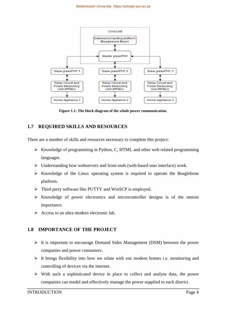
Figure 1.1: The block diagram of the whole power communication. ........................................ 4
Figure 2.1: Shows the relationships between HPGP, HPAV AND HPAV2 [12] ..................... 9
Figure 2.2: Constellation mapping [online]. ............................................................................ 13
Figure 2.3: Comparing PSK to QSPK [15] .............................................................................. 13
Figure 2.4: BER of QPSK and other modulation techniques [16]. .......................................... 14
Figure 2.5: Frequency ranges of NB-PLC and BB-PLC [online]. ........................................... 15
Figure 2.6: Explanation of HAN, NAN and WAN [21]. ......................................................... 18
Figure 2.7: Noise in a PLC [online]. ........................................................................................ 20
Figure 2.8: A setup to measure attenuation [26]. ..................................................................... 21
Figure 2.9: Attenuation in an urban area [26]. ......................................................................... 21
Figure 2.10: The Set up to measure Impedance [26]. .............................................................. 22
Figure 2.11: The modelling of impedance in a PLC [30]. ....................................................... 22
Figure 2.12: Impedance in an urban area [26]. ........................................................................ 23
Figure 2.13: Effect of household appliance over power line impedance [26]. ........................ 23
Figure 3.1: The over view of the power line communication system. .................................... 25
Figure 3.2: CS5490 Pin Description [32] ................................................................................ 26
Figure 3.3: Internal blocks making the CS5490 [32] ............................................................... 27
Figure 3.4: CS5490 and the current sensing resistors (422 KOhms) RPMU circuit. .............. 30
Figure 3.5: TRACO POWER [33] ........................................................................................... 31
Figure 3.6: 3.3V relay. ............................................................................................................. 31
Figure 3.7: SMD MOSFET [35] .............................................................................................. 32
Figure 3.8: MOSFET as a switch. ............................................................................................ 33
Figure 3.9: Cartridge fuse ........................................................................................................ 33
Figure 3.10: Crystal oscillator 4.096MHz. .............................................................................. 34
Stellenbosch University https://scholar.sun.ac.za

xii
Figure 3.11: Connector and Pinhead. ....................................................................................... 34
Figure 3.12: Beaglebone Black parts [40]. ............................................................................. 35
Figure 3.13: The frontal picture of HPGP. .............................................................................. 37
Figure 3.14: The Back of the HPGP. ....................................................................................... 37
Figure 3.15: Oscilloscope outputs a test character from the HPGP UART. ............................ 40
Figure 3.16: QCA7000 and MK20DX256VMC7 [42]. ........................................................... 40
Figure 3.17: Circuit board of RPMU. ...................................................................................... 41
Figure 4.1: Visual representation of the mains program on the Beaglebone Black. ............... 44
Figure 4.2: Beaglebone Black mains program flow diagram. ................................................. 45
Figure 4.3: Desktop OS versus RTOS [44]. ............................................................................ 46
Figure 4.4: Flow diagram of the program running in the master greenPHY. .......................... 47
Figure 4.5: Flow diagram of the program running in the slave HPGP. ................................... 48
Figure 4.6: HPGP‟s UART Rx flow chart. .............................................................................. 49
Figure 4.7: HPGP‟s UART TX flowchart. .............................................................................. 50
Figure 4.8: Byte counter flowchart .......................................................................................... 51
Figure 4.9: Parser to switch off devices. .................................................................................. 52
Figure 4.10: Flow chart of the Loop Driven CRC. .................................................................. 53
Figure 4.11: Data 8-bit byte frame. .......................................................................................... 54
Figure 4.12: The UART register on a CS5490 [32]................................................................. 54
Figure 4.13: Reading CS5490 registers. .................................................................................. 55
Figure 4.14: Diagram for writing and sending instruction to the CS5490 serially. ................. 55
Figure 5.1: First interface. ........................................................................................................ 59
Figure 5.2: Second designed interface using Freeboard.io and Dweet.io. ............................... 61
Figure 5.3: Raphael‟s Justgage. ............................................................................................... 62
Figure 5.4: Client server interactions. ...................................................................................... 63
Figure 5.5: Final designed interface using Tornado websocket, Javascript, HTML and CSS.63
Stellenbosch University https://scholar.sun.ac.za

xiii
Figure 5.6: Data in JSON format at the client-side (web-based user interface). ..................... 64
Figure 6.1: Various existing network structure [online]. ......................................................... 69
Figure 6.2: Point-to-point connection of one master and one slave greenPHY. ...................... 70
Figure 6.3: The bus topology in a home. ................................................................................. 71
Figure 6.4: MME data frame in relation to HDLC-like packet. .............................................. 72
Figure 6.5: Formation of MME and data messages on the HPGP module. ............................. 72
Figure 6.6: Data acquisition scheme from the power line. ...................................................... 73
Figure 7.1: The experimental setup for the testing. ................................................................. 75
Figure 7.2: The time domain measurements of the mains. ...................................................... 76
Figure 7.3: The frequency domain measurement of the mains. ............................................... 77
Figure 7.4: The distortion on the mains. .................................................................................. 78
Figure 7.5: A zoomed in version on the distortion in time domain. ........................................ 78
Figure 7.6: The frequency domain shows the sub-carriers of a HPGP. ................................... 79
Figure 7.7: The graph of error vs. distance for a slave HPGP module and the Command unit.
.................................................................................................................................................. 80
Figure 7.8: Error vs distance for two slave HPGP module and the command unit. ................ 81
Figure 7.9: Snippet of packet test result from PUTTY. ........................................................... 82
Figure 7.10: Arrival time for 40 packets. ................................................................................. 84
Figure 7.11: Communication system on the Power line. ......................................................... 85
Figure A.1: J-Link debugger .................................................................................................... 93
Figure A.2: Shell for J-Link ..................................................................................................... 94
Figure A.3: The connection between target, host and a debugger. .......................................... 95
Figure C.1: RPMU PCB Component layout. ........................................................................... 98
Figure C.2: Top layer of the RMPU PCB. ............................................................................... 98
Figure C.3: Bottom layer of the RPMU PCB. ......................................................................... 99
Figure C.4: Schematic of the RPMU. .................................................................................... 100
Stellenbosch University https://scholar.sun.ac.za

xiv
LIST OF TABLES
Table 1: Comparing NB-PLC to BB-PLC ............................................................................... 11
Table 2: The pin out of CS5490. .............................................................................................. 29
Table 3: UART on Beaglebone Black ..................................................................................... 36
Table 4: Serial Wire Debug (SWD) Connector on (HPGP Module) ....................................... 38
Table 5: Client Side Connector on PLC Stamp 1 evaluation board. ....................................... 38
Table 6: UART on the PLC Stamp 1 evaluation board (HPGP Module). ............................... 39
Table 7: CS5490 useful commands. ........................................................................................ 56
Table 8: Table for CS5490 useful parameters. ........................................................................ 57
Table 9: Structure of HDLC-like packet. ................................................................................. 67
Table 10: The data fields in the data packet for different events. ............................................ 67
Stellenbosch University https://scholar.sun.ac.za

xv
PUBLICATION
A. Ogunleye, P.J Randewijk , R. Wolhuter , “Design and Implementation of a Power Line
Carrier Communication System using Home Plug GreenPHY𝑇𝑀 for Demand Side
Management (DSM)”, “ Smart grid SAIEE conference Johannesburg”, Feburary, 2015.
Stellenbosch University https://scholar.sun.ac.za
xvi
LIST OF ABBREVIATIONS
AC Alternating Current
AMR Automatic Meter Reading
API Application Peripheral Interface
AVLN Audio and Video Logical Network
BBB Beaglebone Black
BER Bit Error Rate
BJT Bipolar Junction Transistor
BPL Broad band over Power Line
CAN Controller Area Network
CMOS Complementary Metal Oxide Semiconductor
CRC Cyclic Redundancy Check
CSS Cascading Style Sheet
DC Direct Current
DSM Demand Side Management
DSSS Direct Sequence Spread Spectrum
EMI Electromagnetic Interference
GPIO General Purpose Input and Output
HAN Home Area Network
HDLC High Level Data Link Control
HDTV High definition Television
HTML Hyper Text Markup Language
HPGP Home Plug GreenPHY𝑇𝑀
IC Integrated Circuit
IEEE International Electrical and Electronics Engineering
Stellenbosch University https://scholar.sun.ac.za

xvii
IoT Internet of Things
LAN Local Area Network
LED Light Emitting Diode
LIN Local Interconnect Network
MAC Media Access Control
MME Message Management Entry
MOSFET Metal Oxide Silicon Field Effect Transistor
OFDM Orthogonal Frequency Division Multiplexing
PLC Power Line Carrier
PRIME PoweRline Intelligent Metering Evolution
QAM Quadrature Amplitude Modulation
QoS Quality of Service
QPSK Quadrature Phase Shift Key
ROBO Robust Modulation
SPI Serial Peripheral Interface
SPST Single Pole Single Throw
SMD Surface Mount Device
SWD Serial Wire Debug
UART Universal Asynchronous Receiver and Transmitter
VoIP Voice over Internet Protocol
WAN Wide Area Network
Stellenbosch University https://scholar.sun.ac.za

INTRODUCTION Page 1
CHAPTER 1
1 INTRODUCTION
1.1 OVERVIEW
This project involves the design and implementation of an embedded Home Plug
Green𝑃𝐻𝑌𝑇𝑀 Web-based system for Demand Side Management in smart home applications.
The project enables management of power consumed by low-power consumers (homes) as
well as high-end power consumers (Industries and Offices). The Internet could be
considered to control how we interact with our home gadgets, appliances and industrial
machinery. Demand Side Management (DSM) refers to an alliance formed between power
supply companies and consumers on how to compensate and help each other during a peak
demand period. Depending on the agreement, home appliances could be switched off
remotely by either the power companies or customers in order to reduce the load and allow
more power to be available during peak periods [1].
This system which has been built can be divided into software and hardware. A computing
platform (Beaglebone Black) and Home Plug GreenPHY𝑇𝑀 (HPGP) evaluation module from
I2SE, the PLC Stamp 1, are the major hardware parts; while other devices such as relays,
circuit protection devices and power measuring device are the minor hardware. The software
includes the websocket application, the webpage to be rendered, the Angstrom OS running on
the platform (Beaglebone Black) and programs written to control the Beaglebone Black and
the HPGP module operation.
1.2 PROBLEM STATEMENT
This project is a prove of concept to show that I2SE‟s HomePlug GreenPHY𝑇𝑀 module can
be use for a smart home application that can participate in Demand Side Management.
Stellenbosch University https://scholar.sun.ac.za

INTRODUCTION Page 2
1.3 PROJECT MOTIVATION
Shortly before the end of 2014, South Africa experienced some load shedding and blackouts
caused by a multitude of problems at ESKOM, the national utility of South Africa [2] and [3].
In 2007, the demand for electricity was higher than the supply and the bad maintenance
culture in generating plants resulted in a black-outs in some part of South Africa [3]. Black-
outs affect the economy and the social activities of the country, because multinational
companies like mining companies run below full capacity while the small and medium
business ventures are also thrown into darkness due to lack of emergency generators. Rolling
out additional power generating stations to support the national grid is not forthcoming due to
the slow decision making process and lack of funding.
Smart grid technology can be used to counter these occurrences, although it is not a
permanent solution to the energy crisis. Homes and business ventures could participate in
Demand Side Management (DSM) in such a way that power companies can mail or text
participants to shut down for a period of time and be rewarded with energy units or monetary
rewards [4]. Home/Office owners need not be at home to participate in DSM since the power
communication interface created for the smart homes/offices is remote.
1.4 AIM
The aims of this project are:
Evaluating the options for implementing a home DSM system.
Creating a feasible systems design for such a system.
Designing a Power line communication system for DSM using HPGP module from
I2SE group.
Designing a web-based User Interface to interact with the hardware.
Evaluating the influence of power line noise disturbances on the system.
1.5 PROJECT DESCRIPTION
The purpose of this project is to design a user friendly, easily customizable based on
using the power measuring integrated circuit, e.g. the CS5490 from Cirrus, the Home
Stellenbosch University https://scholar.sun.ac.za
INTRODUCTION Page 3
Plug GreenPHY𝑇𝑀 (HPGP) module, and a computing platform (Beaglebone Black) to
serve as a gateway and an information collation centre.
The project has a web-based interface that renders vital parameters like power and
current consumed by devices in real time and is very responsive to users.
A communication protocol has been developed to frame command and response
intelligently between the systems. The paradigm of a master-slave topology has been
used extensively between the HPGP modules in the power line communication
system.
The project consumes a minimal amount of power compared to the overall power
consumed by the devices to be controlled, and the design is financially feasible.
A database is incorporated into the design to store a time stamped data for later
analysis of the system.
1.6 TECHNICAL APPROACH
Designing a client side web-based dashboard.
Creating a websocket to allow bi-directional flow of data from client to server using
tornado websocket.
Setting up serial communication between our Linux based computer, the Beaglebone
Black and the HPGP module.
Program the HPGP module with a JTAG.
Design a Relay and a Power Measuring Unit (RPMU) with an energy measuring
integrated circuit that serially communicates with a HPGP module sending useful data
such as current and voltage to the websockets, and allows for switching connected
appliances.
Calibration of measuring inputs to the system and evaluation of the effect of PLC
borne disturbances.
Stellenbosch University https://scholar.sun.ac.za
INTRODUCTION Page 4
Figure 1.1: The block diagram of the whole power communication.
1.7 REQUIRED SKILLS AND RESOURCES
There are a number of skills and resources necessary to complete this project:
Knowledge of programming in Python, C, HTML and other web related programming
languages.
Understanding how webservers and front-ends (web-based user interface) work.
Knowledge of the Linux operating system is required to operate the Beaglebone
platform.
Third party software like PUTTY and WinSCP is employed.
Knowledge of power electronics and microcontroller designs is of the utmost
importance.
Access to an ultra modern electronic lab.
1.8 IMPORTANCE OF THE PROJECT
It is important to encourage Demand Sides Management (DSM) between the power
companies and power consumers.
It brings flexibility into how we relate with our modern homes i.e. monitoring and
controlling of devices via the internet.
With such a sophisticated device in place to collect and analyse data, the power
companies can model and effectively manage the power supplied to each district.
Stellenbosch University https://scholar.sun.ac.za
INTRODUCTION Page 5
1.9 THESIS OUTLINE
In chapter 2 an overview of the background studies for a power line communication
system and other existing technologies for a smart grid application is presented.
In chapter 3 the hardware, the theory behind choosing components and module used
for the implementation of the power line communication system are discussed.
Chapter 4 provides an insight into the embedded software of the project. Firmware
developed for the HomePlug GreenPHY𝑇𝑀 (HPGP) module in embedded C
programming language, Python script and open source libraries such as Adafruit
library was written for the Linux based computer, the Beaglebone Black is
extensively discussed in this chapter.
In chapter 5, the web-based dashboard developed for the project and the websocket
implemented for this project are explained.
Chapter 6 discussed the power line communication topology and protocols developed
for the project. The packet used on the network is adequately explained in this section.
Chapter 7 present the results, testing and measurements for the project.
Chapter 8 discusses the recommendation and conclusion of the thesis.
Appendices.
Stellenbosch University https://scholar.sun.ac.za
LITERATURE REVIEW Page 6
CHAPTER 2
2 LITERATURE REVIEW
2.1 POWER LINE COMMUNICATION
Power Line Communication (PLC) is a unique and a robust way of transmitting signals by
utilizing the existing medium of communication around a house, factory or office as the case
maybe. In most power lines, a frequency of 50Hz to 60Hz already exist, and it is taken into
consideration before modulating it with a higher frequency and demodulating where the
signal is needed. Most countries of the world regard unshielded wire transmission as radio
transmitters, therefore limiting the transmission to below 500 KHz. The United States permit
the transmission of limited-wide-band signals so that the cable used cannot propagate radio
waves [5]. Ground breaking work has been done to perfect this act and we now have internet
services connected to computer systems, using the power lines “Broadband over Power
Lines” (BPL) technology. The signal sent around could be used for meaningful things like
remotely controlling the appliances in your homes by sending control signals. Companies like
control4 and HomeSeers are making a fortune by customizing smart solutions for homes
using PLC and other wireless technologies like WiFi and Zigbee. Development of smart grid
applications is a rapidly emerging field of technology that is transforming the way we do
things, making human endeavours efficient and worth-while.
Power Line Communication (PLC) transverses across telecoms, power electronics and signal
processing. The application of PLC to smart grid technology bring about automatic meter
reading (AMR), Broad Band over Power lines BPL and further extends into automotive
industries like Electric Vehicle Charging stations (EV). Like any other technology, power
line communication has its short comings such as noise harmonics generated by connected
devices, attenuation, interference with radio signals and incompatibility with the existing
wiring structures. These issues can be eased by using state of the art power line carrier
modems, allowing engineers to implement the best technology that suits the vicinity where
the power line communication will be used.
Stellenbosch University https://scholar.sun.ac.za
LITERATURE REVIEW Page 7
2.2 BRIEF HISTORY OF POWER LINE COMMUNICATION
Power line communication has been in existence since the 1950‟s in the form of street
lighting and tele-remote relay applications, [5] and [6]. In the year 1990, internet over Power
lines began to manifest itself with technologies like X-10, CEBus and LonWorks, [7] and [8]
and [6]. Ascom (Switzerland) and the Norweb (U.K.) researched and perfected the first bi-
directional data signal transmission over the power lines [6]. Before this however, in
1980,then, work was done using power lines to uni-directionally transmit data between 5 and
500kHz [9].
2.3 HOMEPLUG POWER LINE ALLIANCE
The alliance was created to lay down the standards so that appliances could relate with each
other over the already existing electrical wires, and also serves as a medium for the Internet.
Appliances connected using some power line technologies suffer electrical noise during
switching. This noise in turn affects the quality of the data transmitted by flipping the bits
along the power lines. Thorough testing of the technology was performed on 500 homes in
America by HomePlug Alliance member such as Qualcomm, Cisco and Texas Instrument to
name but a few.
HomePlug 1.0 was introduced in June 2001 and was subsequently followed by HomePlug
AV in 2005; speeding up the rate of bit transfer from 14 to 200 Mbit/s in the physical layer.
In 2010, HomePlug GreenPHY was standardised and applied to the smart energy
technologies which are still an evolving field today. IEEE on September 30 2010 devised
standard IEEE‟s 1901 (Broadband and Power line Standard) as a baseline technology for the
FFT-OFDM PHY. OFDM modulation enables the different carriers to coexist and be
transmitted on the same electrical wiring. HomePlug can be characterised into HomePlug
GreenPHY, HomePlug AV and the HomePlug AV2 which can inter-relate with one another
[5].
Apart from HomePlug Power line Alliance, other regulatory standards exist such as
CENELEC ENG1107, the Consumer Electronics Association (CEA) R7, The Institute of
Electrical and Electronics Engineering (IEEE), Standard Institute (ETSI) and The PLC forum
European Telecommunication and the Institute of Electrotechnical Commission (IEC).
Stellenbosch University https://scholar.sun.ac.za

LITERATURE REVIEW Page 8
2.4 HOMEPLUG VERSIONS AND USES
2.4.1 HOMEPLUG 1.0
The protocol in this module is based on equally spaced 128-carrier Orthogonal Frequency
Division Multiplexing (OFDM) within the range 0 to 25 Hz. It uses Viterbi and Reed
Solomon coding with interleaving for payload data and turbo product code for controlling
data. HomePlug 1.0 uses a band of frequency between 4.5 MHz to 21 MHz. It runs at a PHY-
rate of 14 Mbit/s and was incorporated by the Telecommunications Industry Association
(TIA) into TIA-1113 which standardized the use of modem on an electrical wiring. This
therefore created a high speed megabit power line communication standard that was generally
accepted. Transmission of vital messages on HomePlug 1.0 is done on the Robust
Modulation (ROBO) mode. Attenuation prevents detection of collision in HomePlug 1.0
which is why it uses CSMA/CA for the MAC protocol. The four levels of priority in the
CSMA/CA scheme are used for MAC layer in HomePlug 1.0. This scheme requires the node
to sense the medium before data transmission. If there is a current transmission going on in
the medium, this delays its transmission until the current transmission is stopped. A 56-bit
Data Encryption Standard (56-bit DES) is used on HomePlug1.0 and, for the sake of security,
adaptive window size management technique for security.
2.4.2 HOMEPLUG GREEN𝐏𝐇𝐘𝑻𝑴 (HPGP)
The HPGP has a bit rate of 10 Mbit/s and it was designed for smart grid applications.
HomePlug GreenPHY𝑇𝑀 (HPGP) is the version used specifically for this project to integrate
appliances in a vicinity to form a network [6]. The HPGP is a derivative of the HomePlug AV
and it is more energy efficient than HomePlug AV [6]. It is also used as plug-in for electric
vehicles to connect it to the grid for charging and data exchange.
2.4.3 HOMEPLUG ACCESS BPL
BPL means broad band over power line. It was authorized in June 2005 and merged with the
IEEE 1901 standard. This power line technology allows high-speed digital data transmission
on electrical cables used for power distribution. Frequencies as high as the radio spectrum are
used in this technology to transmit data over long distances. Interference mitigates BPL
communication and adequate measures are put in place to counter this. It is a very convenient
Stellenbosch University https://scholar.sun.ac.za

LITERATURE REVIEW Page 9
technology because BPL modems can be plugged to the wall outlet so as to supply internet
access to various power outlets in the house.
2.4.4 HOMEPLUG AV
HomePlug AV is the abbreviation used for HomePlug Audio and Video. It has a higher
bandwidth for VoIP and HDTV and was introduced in August 2005. It has a bit rate of about
80 Mb/s at the MAC layer and 200 Mb/s at the physical layer for high speed communication.
HomePlug AV can achieve near theoretical maximum bandwidth across a given transmission
path using adaptive modulation up to 1155 OFDM sub-carriers, two-level MAC framing with
ARQ and turbo convolution codes for error correction [10]. Devices that use HomePlug AV
should be interoperable with one another. 128 bit AES encryption and key distribution
techniques are used for security reasons [11].
2.4.5 HOMEPLUG AV2
HomePlug AV2 was introduced in January 2012 and can freely communicate with HomePlug
Green PHY and HomePlug AV. Its bandwidth ranges between 30 MHz to 86 MHz features
gigabit-class PHY-rate, power saving modes and allowing MIMO PHY [12]. It was first sold
as HomePlug 600 which is two tenth times faster than HomePlug AV 500.
Figure 2.1: Shows the relationships between HPGP, HPAV AND HPAV2 [12]
Stellenbosch University https://scholar.sun.ac.za

LITERATURE REVIEW Page 10
2.4.6 OTHER POWERLINE MODULES
2.4.6.1 G3-PLC
This is another trending power line module apart from the Home Plug technologies. It
supports high-speed, IP-based communication over the power lines. The module is based on a
narrowband power line communication with a longer range than the Home Plug modules.
The data rate is also slower and has a narrow frequency unlike the Home Plug modules. Its
modulation scheme is based on Differential Quaternary Phase-Shift Keying (DQPSK) or
Differential 8-Phase-Shift Keying (D8PSK).
2.4.6.2 PRIME
PoweRline Intelligent Metering Evolution (PRIME) is a narrow band PLC module having a
frequency band up to 500 KHz. It also operates in ARIB, FCC and CENELEC bands and has
a Baud rate of 128kps. It is based on OFDM and has a modulating scheme of DBPSK,
DQPSK or D8PSK. It uses convolutional code for Forward Error Correction (FEC).
2.5 PLC COMPARED TO WIRELESS SMART GRID TECHNOLOGIES
The power tussle between the application of wired and wireless technology has no definite
winner or loser, they both have their clear advantages and disadvantages. For instance,
connecting the house with internet via power line module is inexpensive because the existing
medium which is the house wiring had already been laid. A carrier used attenuate depending
upon the transmission method. The signal being power line borne is less subjected to physical
barriers, like 802.1l signals.
2.6 CLASSIFICATION OF POWER LINE COMMUNICATION NETWORK
We have two classifications of power line communication, the Narrow Band PLC (NB-PLC)
usually below 500 kHz and the Broad Band PLC (BB-PLC) usually higher than the 1.8 MHz
and with a data rate of over 1 Mbps. Narrow band can be further divided into Home control
narrow band, Low-speed narrow band and Medium-speed narrow band.
Stellenbosch University https://scholar.sun.ac.za

LITERATURE REVIEW Page 11
Table 1: Comparing NB-PLC to BB-PLC
Narrowband PLC Broadband PLC
Uses Gaming, Internet and
HDTV
Advanced Metering,
Smart homes, Street
Lighting and Electric
vehicle
Data rate Less than 200 kbps More than 1 Mbps
Modulation OFDM, FSK, S-FSK,
BPSK and SS
OFDM
Frequency Up to 500 kHz More than 2 MHz
2.7 HOME-CONTROL NARROW BAND
This is a PLC technology that is commonly used in Home Area Network (HAN). The
modulating carrier is between 20 and 200 KHz and is transmitted on the electrical wire of
homes. This system consists of the encoder at the transmitter part and the decoder at the
receiver part with the gadget to be controlled. Addressing systems are employed in order to
control a specified gadget/appliance on the grid. Devices participating in this network are
plugged to the various mains of a household. The transmitting device may be in the lobby and
the receiving device in the kitchen for this type of application.
2.8 LOW-SPEED NARROW BAND
Low-speed narrow band is mostly used for remote meter readings on high tension wires and
its carrier frequency operates between 9 and 500 kHz. It has been used in consumer products
since 1940. The data rate of most narrow band applications is less than 10 kbps. Modulation
techniques peculiar to it are FSK, BBPSK, FFH SFSK and DCSK [13].
2.9 MEDIUM-SPEED NARROW BAND
Its data rate is between 50 kbps and 1 Mbps and the frequency is between 9 and 500 kHz for
A-Band, 9 and 95 kHz B-Band, 95 and 125 kHz BCD-Band [13]. The modulations mostly
Stellenbosch University https://scholar.sun.ac.za

LITERATURE REVIEW Page 12
used for these bands are OFDM and MCM. Applications of medium-speed narrow band are,
Airfield Lighting, Automated Meter Reading (AMR) and Smart Grids.
2.10 BROAD-BAND
For broadband PLC, the frequency spectrum exists between wide bands especially the 1 MHz
to 30 MHz. It is very robust and not affected by noise disturbances because of the
implementation of spread spectrum technology. HomePlug technologies use broad-band and
sabotaging data on power line using broad-band is challenging compared to narrow band.
Higher data rate 4 Mbps to 500 Mps is achievable with modules based on this technology.
2.11 PLC MODULATION
BB-PLC makes use of multi-carrier modulation techniques while NB-PLC makes use of
single carrier modulation techniques. Modulations such as FSK, S-FSK, BPSK and OFDM
can be used for NB-PLC unlike BB-PLC which only uses OFDM.
2.11.1 SINGLE–CARRIER MODULATION
For this type of technique, digital data are represented using a specified signal. Phase-Shift
Keying (PSK), Amplitude-Shift Keying (ASK) and Frequency-Shift Keying (FSK) are based
on this scheme. The characteristic (frequency or phase) of a reference signal is modulated by
the transmitted data. Reliability; reduced power consumption and low cost are the advantages
of using this modulation technique. Distortion and noise are the main challenges mitigating
the Single-Carrier modulation and these can be improved by correction mechanisms and error
detection mechanisms. Example of products that makes use of this scheme are X-10 (using
ASK) and Echelon‟s transceivers (using BPSK). Merging PSK and ASK produces QAM
(Quadrature Amplitude Modulation). A constellation of 4-QAM, 8-QAM, 16-QAM and 32-
QAM exists. Single-Carrier modulation is well suited to Power Line Communication (PLC)
because it is easily implemented. It is not easily adaptable to broadband PLC due to its high
speed communication over power line medium. Single-Carrier modulation is not adequate for
PLC communication because a spectral efficiency of only about 1 bit/s per Hz can be
achieved [14].
Stellenbosch University https://scholar.sun.ac.za
LITERATURE REVIEW Page 13
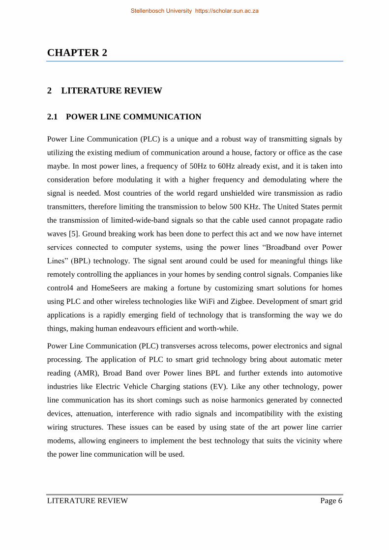
Figure 2.2: Constellation mapping [online].
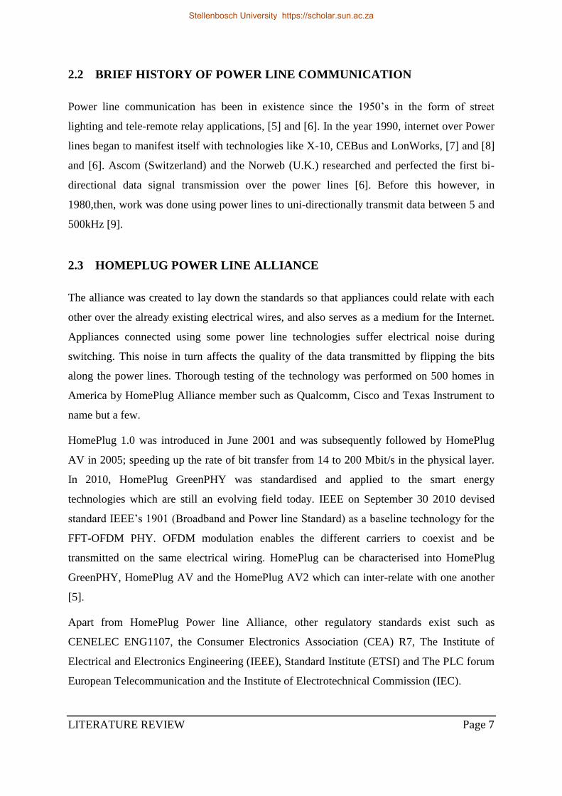
2.12 HOME PLUG GREENPHY’S MODULATING TECHNIQUE (QPSK)
For HPGP, the modulating technique used is QPSK and it is also known as 4QAM or 4-PSK.
QPSK is a variant of PSK in which two bits are modulated at once and can appear at any of
the four possible carrier phase shift of 0, 90, 180 or 270 degrees. The 4 points on the
constellation diagram are equally spaced around a circle, therefore it can convey twice as
much information as BPSK (two bits per symbol). The BER graph in Figure 2-4 shows that
the BPSK and QPSK have the same error performance and performs less efficiently than the
other PSK variant as shown in figure 2-3.
Figure 2.3: Comparing PSK to QSPK [15]
Stellenbosch University https://scholar.sun.ac.za

LITERATURE REVIEW Page 14
Figure 2.4: BER of QPSK and other modulation techniques [16].
2.13 SPREAD-SPECTRUM MODULATION
This is a modulating technique in which the bandwidth is spread in the frequency domain
resulting in a wider bandwidth signal. The spread spectrum was initially developed for
military use because of its robustness against interference. It is resistant to eavesdropping,
jamming and fading of signal and its signal structuring technique uses direct sequence,
frequency hopping or a combination of these which can be used for multiple access. Jamming
spread spectrum is harder to implement compared to narrowband signals and series of spread
spectrum existed. The spread-spectrum has a lower Power Spectral Density (PSD) which is in
line with EMC and attractive for Power Line Communication. There are various types of
spread spectrum which are time hopping, frequency hopping, Direct-Sequence Spread
Spectrum (DSSS), chirp and hybrid techniques. The part of spread spectrum modulation that
helps to combat narrow band interference by spreading the interference signal over a wide
bandwidth.
Stellenbosch University https://scholar.sun.ac.za

LITERATURE REVIEW Page 15
2.14 ORTHOGONAL FREQUENCY DIVISION MULTIPLEXING (OFDM)
This is a method of digital modulation where signals are split into several narrow channels at
different frequencies. It is a robust modulation technique that is well-proven in high speed
wired and wireless applications. OFDM is a type of Multi-carrier transmission suited to
selective channels and high data rates [17]. In OFDM, data transmission occurs at a high
speed by spreading the data over a large number of sub-carriers each of which are modulated
at low rates.
Figure 2.5: Frequency ranges of NB-PLC and BB-PLC [online].
2.15 COMMUNICATION STRATEGY ON THE MEDIUM
In a power line communication network, data has to flow from one point to the other, for
example, from a master to a slave on the physical medium and techniques that prevent
collision need to be employed. Medium access methods are an industrially viable technique
to is suited for such an application and examples of it are token passing, contention and
polling.
Stellenbosch University https://scholar.sun.ac.za

LITERATURE REVIEW Page 16
2.15.1 TOKEN PASSING
The word “token” refers to a unique string identifier by which an interaction can be
authenticated. On the medium, a data frame allows a specific device to transmit while others
wait or listens. The token is discarded after transmission is complete and other devices on the
network acquire the token to initiate transmission.
2.15.2 CONTENTION
This medium access technique makes use of Carrier Sense Multiple Access with Collision
Detection or Collision Avoidance (CSMA/CD or CSMA/CA). Before any device transmits
data, it listens on the medium whether a device is currently transmitting its data, if not, it
initiates transmission. When two devices transmit data at the same time, collision occurs and
the two devices stops transmission, wait a while and re-initiate transmission.
2.15.3 POLLING
Polling techniques is well established. In this medium access technique, the master
continuously queries for data from the slaves. Any time there is new data, the slave is allowed
to transmit on the network medium. Polling wastes a lot of CPU cycles that could be used for
other important executions, but is very robust.
2.15.4 ALOHA
This is a technique in which when a device on the channel is ready to transmit a data packet,
it starts transmitting the packet without first verifying if the channel is busy. The packet is
destroyed if collision occurs between packets from two different devices. Retransmission of
the destroyed packet occurs at a random time in the future. This technique is simple
compared to other data transmission protocols, but the QoS of ALOHA is poor under heavy
network traffic. Its performance can be enhanced by dividing the transmission channel into
time slots. Devices can initiate transmission at the beginning of the time slot and this
improved technique is called slotted ALOHA.
2.16 SMART GRID NETWORK
Smart grid network uses the principle of communication and electrical technology to provide
an efficient, intelligent and reliable power distribution and generation system that is flexible
Stellenbosch University https://scholar.sun.ac.za

LITERATURE REVIEW Page 17
enough to allow exchange and documentation of information between the consumer and
power companies. The use of smart meters came into the picture around the 1980s to monitor
energy consumed by large consumers of electricity and was later improved to document the
use of power with the time of the day in 1990 [18]. Smart grid network can be divided into
the Home Area Network (HAN), Neighbourhood Area Network (NAN) and the Wide Area
Network (WAN).
2.16.1 HOME AREA NETWORK (HAN)
The HAN is an intelligent network formed with various home appliances and can be used to
monitor the energy consumed and to remotely control the smart appliances in close vicinity
such as home. HVAC (Heating, Ventilation and Air Conditioning) systems are becoming
smarter by adding microcontrollers that locally control them and relay their state to other
intelligent modules to optimize and save energy consumed by a household. The HAN can
also be called the Business Area Network (BAN) or Industrial Area Network (IAN) as
discussed in [18]. A combination of smart grid technologies like wired (Power line) or
wireless for automation can be used in a sophisticated home. Various manufacturers have
designed different modules such as high speed internet streaming, HDTV and climate control
in a smart home to bring extra comfort to consumers. In most HANs, all the transducers and
sensors are beaming data in the form of packets to a coordinator (computing platform) and
commands are sent from the user interface also known as the client side to control individual
devices on the HAN. The HAN network can be a fully customized solution for a particular
house or office using a network of Plug and Play devices to assist in turning the home into a
smart one. There are an increasing number of vendors manufacturing devices for HAN but
security of such devices is such a great concern.
2.16.2 WIDE AREA NETWORK (WAN)
The WAN network can be established between several homes, distribution and generating
stations in a specified area. It covers a larger geographical area than the HAN and is mostly
built for a particular organization ranging from private to government institutions. The data
rate of WAN is between 10 to 100 Mbps so that it can contain various NAN information
exchanges. Interconnecting LANs at different locations with a Telecommunication Service
Provider (TSP) can be referred to wholly as WAN (Point-to-Point).
Stellenbosch University https://scholar.sun.ac.za
LITERATURE REVIEW Page 18
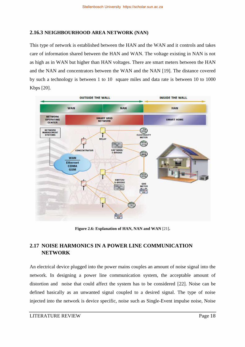
2.16.3 NEIGHBOURHOOD AREA NETWORK (NAN)
This type of network is established between the HAN and the WAN and it controls and takes
care of information shared between the HAN and WAN. The voltage existing in NAN is not
as high as in WAN but higher than HAN voltages. There are smart meters between the HAN
and the NAN and concentrators between the WAN and the NAN [19]. The distance covered
by such a technology is between 1 to 10 square miles and data rate is between 10 to 1000
Kbps [20].
Figure 2.6: Explanation of HAN, NAN and WAN [21].
2.17 NOISE HARMONICS IN A POWER LINE COMMUNICATION
NETWORK
An electrical device plugged into the power mains couples an amount of noise signal into the
network. In designing a power line communication system, the acceptable amount of
distortion and noise that could affect the system has to be considered [22]. Noise can be
defined basically as an unwanted signal coupled to a desired signal. The type of noise
injected into the network is device specific, noise such as Single-Event impulse noise, Noise
Stellenbosch University https://scholar.sun.ac.za

LITERATURE REVIEW Page 19
having line components synchronous with power system frequency, Noise with a smooth
spectra and Non-synchronous noise.
2.17.1 SINGLE-EVENT IMPULSE NOISE
This noise is caused by the on/off switching of a device in a power line network. This is due
to the fact that high level transient voltage is generated within a short period of time by
usually a capacitor, lightning or switching thermostats [23] and [24]. The noise disturbs the
whole frequency band and can exist as a damped oscillation [23]. The Power Spectrum
Density of this noise is very high and can be about 50 dB above the background noise
spectrum [24].
2.17.2 NOISE HAVING LINE COMPONENTS SYNCHRONOUS WITH POWER
SYSTEM FREQUENCY
This type of noise can be characterized as a multiple of the power line frequency (50 Hz or 60
Hz). It exists for a few microseconds and has a Power Spectral Density (PSD) with line
spectra at (50 Hz or 60 Hz). Its decreases with the increase in frequency [24]. Silicon
Controlled Rectifier (SCR) or Triacs generate this type of noise and they are found in light
dimmers. Since this type of noise is synchronous, it is predictable and easily filtered
compared to other types of noise [24]. It can be modelled as impulses and it‟s a bit difficult to
filter because it is unpredictable.
2.17.3 A SMOOTH SPECTRUM NOISE
An appliance that operates asynchronously with the power line‟s frequency produces this
type of noise. Electric motors appliances such as electric drills, mixers, blenders and sewing
machines [24] constitute an example of such appliances in which noise originates from the
brushes inside the motor causing current to switch at a rate which depends on the motor
speed. The noise can be modelled as a white noise over small CENELEC A-band as
discussed in, [25] and [24]. A smooth spectrum without spectra line is a description of this
type of noise. The smooth noise as referred to by [24] is regarded as the “Summation of all
low-power noise sources”. Interleaving in conjunction with Forward Error Correcting (FEC)
codes can be used to get this type of noise [24].
Stellenbosch University https://scholar.sun.ac.za

LITERATURE REVIEW Page 20
2.17.4 NON-SYNCHRONOUS NOISE
The line spectra frequency of an asynchronous noise differs completely from the mains
frequency. It is also referred to as a narrowband background noise [24]. The noise on the
power line network is time dependent and is emitted from sources such as computers,
television stations and AM radio stations [24]. This type of noise can be prevented by
avoiding the problematic frequency as a whole. For example the common television
harmonic frequency of 15.734 Hz should not be used, as suggested by [24].
Figure 2.7: Noise in a PLC [online].
2.18 ATTENUATION ON POWER LINE SYSTEM
Attenuation can be defined as the gradual loss of intensity or signal strength due to the
influence of transversing through a medium and it is measured in decibel (dB). The behaviour
of high frequency signal attenuation has to be measured on a given power line system to
determine the quality of the communication channel provided by the PLC. In [26], the
attenuation was evaluated at frequencies ranging from 10 to 170 KHz (CENELEC A,B,C,D
bands) for phase-neutral, phase-ground, and neutral ground conductors were carried out, and
a PLC attenuation of 4-30 dB was found. To measure attenuation in [26], two transceiver
modems were used, one set up as a receiver and the other as a transmitter. T1 and T2 are
coupling transformers, C is a coupling capacitor and V1 and V2 are AC voltmeters.
Stellenbosch University https://scholar.sun.ac.za

LITERATURE REVIEW Page 21
Attenuation on the power line network is greatly affected by the cable material, type of
wiring topology and load connected to the cable [27].
Figure 2.8: A setup to measure attenuation [26].
According to the graph generated in [26], attenuation in power lines decreases versus
frequency in urban areas after 70 KHz and can be as high as 23 dB in some urban areas [26].
Figure 2.9: Attenuation in an urban area [26].
2.19 IMPEDANCE OF POWER LINE SYSTEM
The combined effect of resistive, capacitive and inductive components attached to a power
line channel to oppose the flow of electrical energy is known as Impedance. According to
Stellenbosch University https://scholar.sun.ac.za

LITERATURE REVIEW Page 22
[28], it causes voltage sags, high frequency noise transient impulses and harmonic voltages.
A well modelled, analysed power line channel is imperative before building the power line
communication system. Some anomalies like EMI and parasitic capacitance can be quite a
challenge. The performance of PLC is a function of network wiring topology, location and
time [28].Working on frequency range of 10 to 170 KHz, impedance was measured at
between 1 to 17 Ohms on an urban power line [26].
For a typical household, the measured impedance is around 1 to 20 Ohms at a frequency of
between 5 to 20 KHz [29]. The simple setup to measure the impedance on a PLC comprises
of a signal generator “SG” and an AC millivoltmeter to measure V1, V2 and V3 on the line.
By default, most PLC modems contain a coupling transformer and capacitor to sense and
transmit on the power lines and most importantly to serve as isolation.
Figure 2.10: The Set up to measure Impedance [26].
Figure 2.11: The modelling of impedance in a PLC [30].
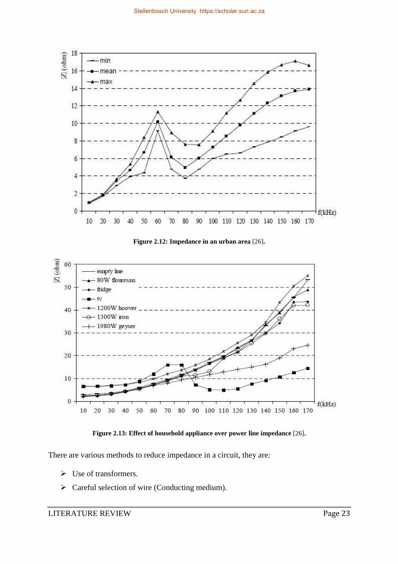
According to the result obtained in figure 2.12, Impedance on a PLC system is a function of
time at a particular frequency which causes the production of a min, mean and max graphs.
According to the graph, there is a local max and resonance at 60 KHz for the urban power
line representation and, according to [26], a sharp decrease between 60 KHz and 80 KHz.
Stellenbosch University https://scholar.sun.ac.za
LITERATURE REVIEW Page 23
Figure 2.12: Impedance in an urban area [26].
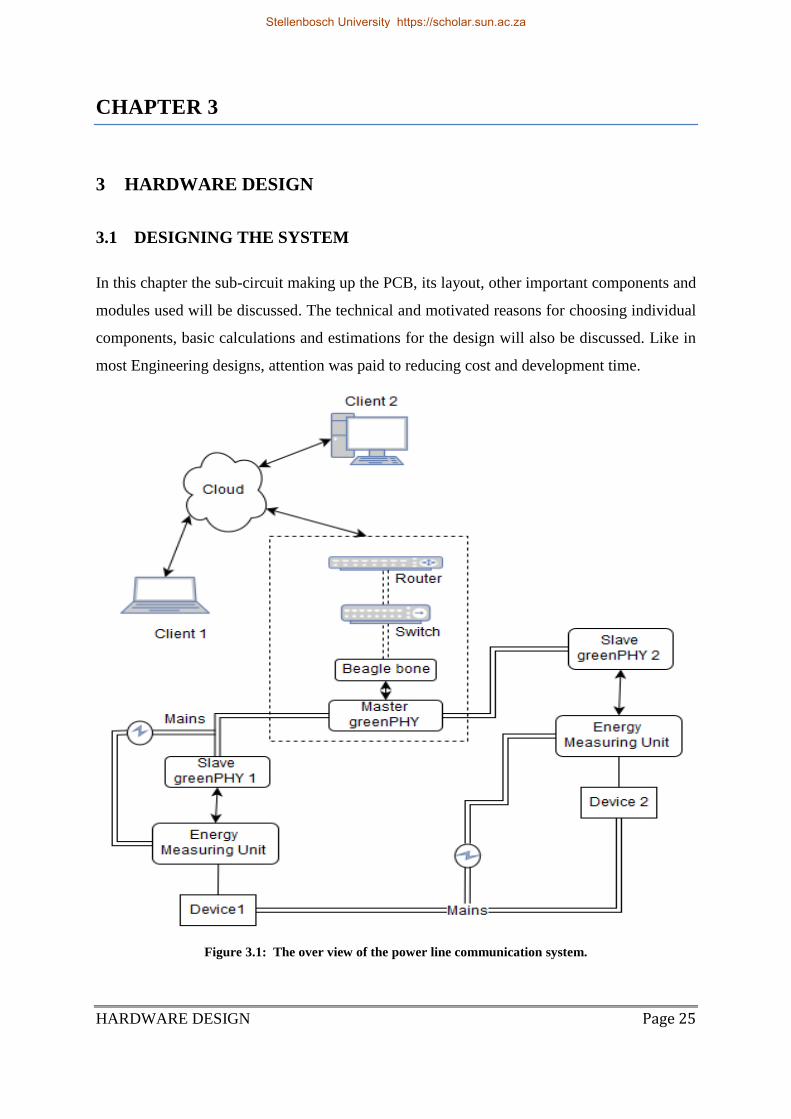
Figure 2.13: Effect of household appliance over power line impedance [26].
There are various methods to reduce impedance in a circuit, they are:
Use of transformers.
Careful selection of wire (Conducting medium).
Stellenbosch University https://scholar.sun.ac.za

LITERATURE REVIEW Page 24
Careful selection of voltage levels.
Distribution of loads on the medium.
2.20 SIGNAL-TO-NOISE RATIO (SNR)
Signal-to-noise ratio is a term coined to test the quality of a desired signal and it is the ratio of
power of the desired signal to power of background noise present in a channel or medium. It
is measured in decibel (dB). A higher SNR means that the communication is very reliable on
a particular channel. To improve the signal-to-noise ratio, a filter has to be coupled to the
communication system to reduce the unwanted signal to the barest minimum. Noise greatly
reduces the distance of propagation in a power line communication channel. The most
commonly found noise on a power line channel is impulsive in nature [31]. The bandwidth of
the channel is a very important factor to consider when calculating the SNR because the noise
passing through the channel directly affects it.
S
N =
Psignal
Pnoise (2-1)
2.21 SUMMARY
This chapter reviews all the existing technologies and provides a short historical background
of power line communication. We also discussed the factors influencing the performance of
power line communication systems and the modulating techniques used.
Stellenbosch University https://scholar.sun.ac.za
HARDWARE DESIGN Page 25
CHAPTER 3
3 HARDWARE DESIGN
3.1 DESIGNING THE SYSTEM
In this chapter the sub-circuit making up the PCB, its layout, other important components and
modules used will be discussed. The technical and motivated reasons for choosing individual
components, basic calculations and estimations for the design will also be discussed. Like in
most Engineering designs, attention was paid to reducing cost and development time.
Figure 3.1: The over view of the power line communication system.
Stellenbosch University https://scholar.sun.ac.za

HARDWARE DESIGN Page 26
3.2 CS5490
This is a cirrus logic CMOS chip that performs onboard power, current and voltage
measurement and calculation by means of analogy-to-digital converters. The energy
measuring chip uses ∆∑ analog-to-digital converters to measure the line current and voltage.
It is a single phase bi-directional chip that communicates with other microcontroller via
UART. CS5490 was considered for the project because most energy measuring chips use SPI
for serial communication examples of such are MCP 3909 and CS5460 also from Cirrus. It is
an accurate chip and it consumes a minute amount of power, about 13 mW [32]. Various
voltage and current censors such as Rogowski coils, current transformers and shunt resistors
can easily interface with the energy measuring chip.
Figure 3.2: CS5490 Pin Description [32]
A reference voltage of 2.4 V is generated on the chip and it provides an analog output via
VREF±. CS5490 is available as a 16-pin SOIC packages which conserve real estate on a
Printed Circuit Board (PCB) [32]. Enticing features of the CS5490 are:
UART connection.
Temperature Sensor.
3.3 V Power Supply.
Very fast on-chip Calibration.
Energy measurement accuracy of 0.1%.
Shunt resistor and Current Transformer (CT) supported.
Voltage sag, voltage swell detection and over current.
A very low power consumption of about 13 mW.
Stellenbosch University https://scholar.sun.ac.za

HARDWARE DESIGN Page 27
On-chip Measurements/Calculations:
Reactive power, active power.
RMS voltage and current calculations.
Power factor and line frequency.
Instantaneous voltage, current, and power.
Figure 3.3: Internal blocks making the CS5490 [32]
The Rx, Tx and the reset are the basic pins needed for communicating with the CS5490 chip
from an external controller. Since high voltage is involved in the PCB, isolation is imperative
to separate the sensitive parts. Optocouplers are used between the HPGP (HomePlug
greenPHY) module and the CS5490. Only three pins need to be isolated making the CS5490
a very attractive choice. The power measuring chips need a voltage divider for voltage
measurement and a shunt for measuring current [32]. 250 mV peak to peak is the maximum
voltage the CS5490 can withstand at both its current and voltage input pins, so extra care
should be taken when choosing components for the design [32]. For the PCB design, a shunt
resistor was chosen due to the fact that it is inexpensive, readily available, smaller and more
reliable than Hall Effect sensors.
Stellenbosch University https://scholar.sun.ac.za

HARDWARE DESIGN Page 28
3.2.1 SHUNT CALCULATION FOR THE CS5490
The 250 mV peak-to-peak maximum voltage was a determinant of the value for the shunt
used. Using Ohms Law,
𝑉𝑚𝑎𝑥 = 𝑅𝑠𝐼𝑚𝑎𝑥 (3-1)
Where 𝑅𝑠 is the shunt resistor.
𝑉𝑚𝑎𝑥 = 250mV, 𝐼𝑚𝑎𝑥 = 16 A
The resulting calculation yielded 15.625 mΩ.
A smaller resistor could be conveniently used since the CS5490 has an internal adjustable
gain of 50 times. Low power dissipation is one of the advantages of using a smaller shunt for
the PCB design.
𝑉𝑟𝑚𝑠 =𝑉𝑀𝐴𝑋/ 2 (3-1)
𝑉𝑀𝐴𝑋=250 mV
𝑉𝑟𝑚𝑠 = 250𝑚𝑉
2
𝑉𝑟𝑚𝑠 =176.78 mV
The 𝑉𝑟𝑚𝑠 is approximately 70.7% of the maximum peak voltage
𝑉𝑟𝑚𝑠 = 𝑉𝑖𝑛 𝑅2
𝑅1+𝑅2 176.78𝑚𝑉 (3-2)
𝑉𝑖𝑛 = 240 𝑉𝑟𝑚𝑠 , 𝑅2=1 kOhm𝑠, 𝑅1 needs to be calculated.
3.2.2 VOLTAGE SENSING
For the voltage sensing aspect of the design, five resistors were used, four of which were 422
kOhms and the other 1 kOhms. The 422 kOhms are connected in series and later connected in
parallel with the 1 kOhms resistor. A design compromise was reached to split the single
resistor value of 1688 kOhms into four different resistors of 422 kOhms in parallel with a 1
kOhms resistor to distribute the heat energy effectively. A through-hole resistor was preferred
Stellenbosch University https://scholar.sun.ac.za

HARDWARE DESIGN Page 29
in this section because it can withstand high voltage and current compared to the SMT
resistors.
Table 2: The pin out of CS5490.
Pin number Name Uses
1 Crystal Out Connect the external crystal.
2 Crystal In Connect the external crystal.
3 Reset An Active Low Schmitt_trigger to
the rest of the chip.
4 IIN- Differential analog input channel
current.
5 IIN+ Differential analogy input channel
current.
6 VIN+ Differential analogy input channel
voltage.
7 VIN- Differential analogy input channel
voltage.
8 VREF- The voltage reference output and
returns.
9 VREF+ The voltage reference output and
returns.
10 GNDA Analog ground.
11 VDDA The positive analog supply.
12 DO Digital output for energy pulses,
Interrupt, energy direction and
zero-crossing.
13 TX UART transmitter pin.
14 RX UART receiver pin.
15 MODE Connect to VDDA for proper
operation.
16 VDDD Decoupling pin for the internal
digital supply.
Stellenbosch University https://scholar.sun.ac.za

HARDWARE DESIGN Page 30
Figure 3.4: CS5490 and the current sensing resistors (422 KOhms) RPMU circuit.
3.3 POWER SUPPLY UNIT
For the design, we decided to use Traco power because of its compactness and generation of
a very smooth DC voltage. TMLM 05103 amongst the different models produces 3.3 volts
and a current of 1250 mA which was enough to power the slave HPGP module, the relay and
the CS5490 Cirrus chip. The researcher designed the traditional transformer-rectifier-filter
circuit as a power section before reverting to use Traco power for fast prototyping. Most of
the devices used in the system from HPGP module to the CS5490 use 3.3 V dc except the
Beaglebone Black that runs off 5 volts. Traco has a series of power sources modules that are
categorized based on the DC voltage, current and its power ratings. The TMLM 05013 has
four terminals, two pins for AC power input, a positive pin and a negative pin.
Stellenbosch University https://scholar.sun.ac.za
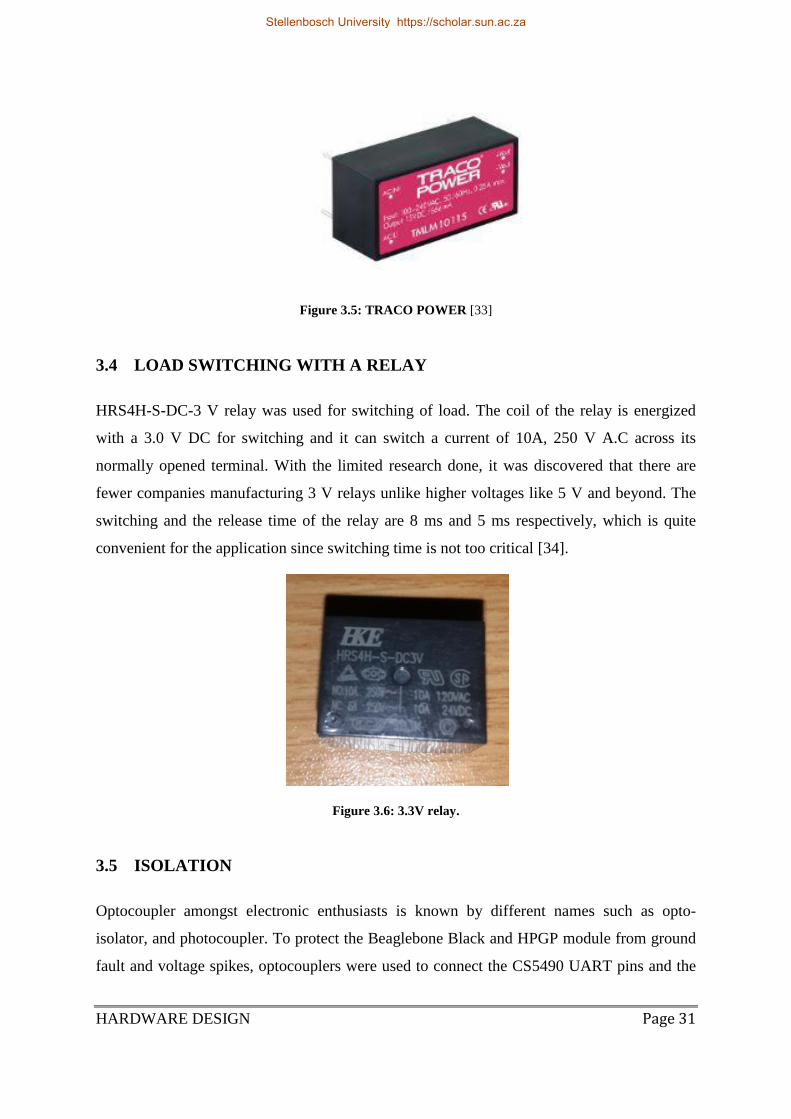
HARDWARE DESIGN Page 31
Figure 3.5: TRACO POWER [33]
3.4 LOAD SWITCHING WITH A RELAY
HRS4H-S-DC-3 V relay was used for switching of load. The coil of the relay is energized
with a 3.0 V DC for switching and it can switch a current of 10A, 250 V A.C across its
normally opened terminal. With the limited research done, it was discovered that there are
fewer companies manufacturing 3 V relays unlike higher voltages like 5 V and beyond. The
switching and the release time of the relay are 8 ms and 5 ms respectively, which is quite
convenient for the application since switching time is not too critical [34].
Figure 3.6: 3.3V relay.
3.5 ISOLATION
Optocoupler amongst electronic enthusiasts is known by different names such as opto-
isolator, and photocoupler. To protect the Beaglebone Black and HPGP module from ground
fault and voltage spikes, optocouplers were used to connect the CS5490 UART pins and the
Stellenbosch University https://scholar.sun.ac.za
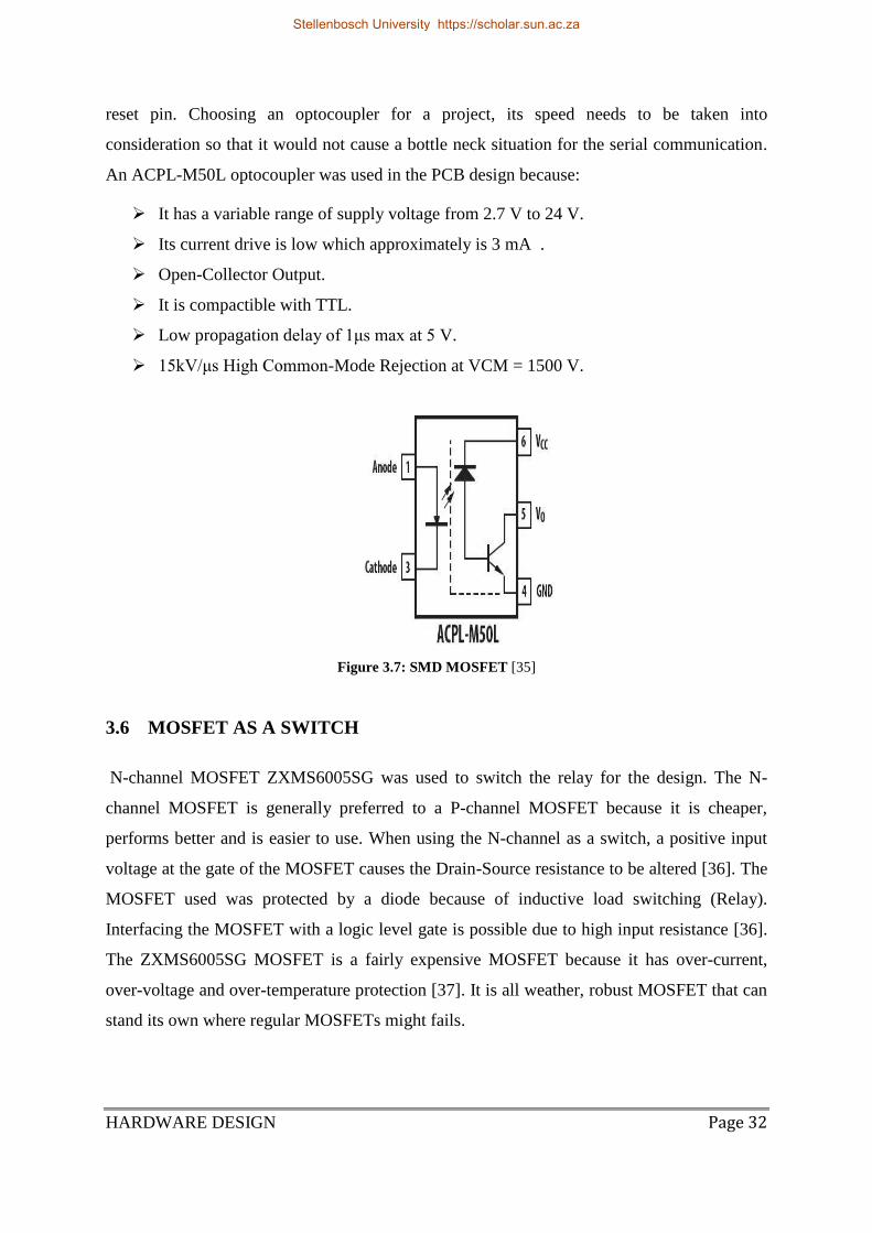
HARDWARE DESIGN Page 32
reset pin. Choosing an optocoupler for a project, its speed needs to be taken into
consideration so that it would not cause a bottle neck situation for the serial communication.
An ACPL-M50L optocoupler was used in the PCB design because:
It has a variable range of supply voltage from 2.7 V to 24 V.
Its current drive is low which approximately is 3 mA .
Open-Collector Output.
It is compactible with TTL.
Low propagation delay of 1μs max at 5 V.
15kV/μs High Common-Mode Rejection at VCM = 1500 V.
Figure 3.7: SMD MOSFET [35]
3.6 MOSFET AS A SWITCH
N-channel MOSFET ZXMS6005SG was used to switch the relay for the design. The N-
channel MOSFET is generally preferred to a P-channel MOSFET because it is cheaper,
performs better and is easier to use. When using the N-channel as a switch, a positive input
voltage at the gate of the MOSFET causes the Drain-Source resistance to be altered [36]. The
MOSFET used was protected by a diode because of inductive load switching (Relay).
Interfacing the MOSFET with a logic level gate is possible due to high input resistance [36].
The ZXMS6005SG MOSFET is a fairly expensive MOSFET because it has over-current,
over-voltage and over-temperature protection [37]. It is all weather, robust MOSFET that can
stand its own where regular MOSFETs might fails.
Stellenbosch University https://scholar.sun.ac.za

HARDWARE DESIGN Page 33
Figure 3.8: MOSFET as a switch.
3.7 FUSE
A fuse rated at 8 Amps was incorporated to serve as a first line of protection for the PCB. It is
a cartridge fuse attached to the plug and not on the PCB. The expected current rating of a
device should not be higher than the rating of the fuse, in fact lower is better so as to create
protection for inrush currents and circuit harmonics [38]. 8 Amp fuse was chosen for
adequate protection of the circuit because the relay used is rated at 250 V A.C at 10amps.
Figure 3.9: Cartridge fuse
3.8 CRYSTAL OSCILLATOR
The crystal oscillator used for the design generates a clock output of 4.096 MHz for the
CS5490 chip. The pins are connected to the XIN and XOUT of the CS5490. The PCB
designed does not have insulated coatings; the body of the crystal oscillator was prevented
from touching the PCB to avoid short circuit.
Stellenbosch University https://scholar.sun.ac.za

HARDWARE DESIGN Page 34
Figure 3.10: Crystal oscillator 4.096MHz.
3.9 CONNECTOR AND PINHEADS
The terminal points where power and signals are fed and received are connected to
connectors and pinheads. The connector used for the PCB is the AK300 which connect to the
power supply and the second one connects the load to the relay. AK300 was chosen because
it could handle high voltages and sit very well on the PCB design. The pinhead used in the
PCB is used to transfered signals to and fro between the HPGP and the energy measuring
PCB. It is suited for low level current and voltage applications and allows for quick
interfacing between devices.
Figure 3.11: Connector and Pinhead.
3.10 BEAGLEBONE BLACK
The computing platform is where data collation, handling and processing takes place.The
Beaglebone Black is based on an ARM cortex-A8 processor that runs Ubuntu, Debian or
Angstrom Linux operating systems and Android [39]. This is an open-source and a collective
initiative of passionate individuals creating a powerful embeddable computer [39]. It is a 32-
bit microcontroller that has an Ethernet port on board to connect it to the internet easily and
64 pin headers for UART, SPI and I2C serial protocols and other specialized functions [39].
Stellenbosch University https://scholar.sun.ac.za
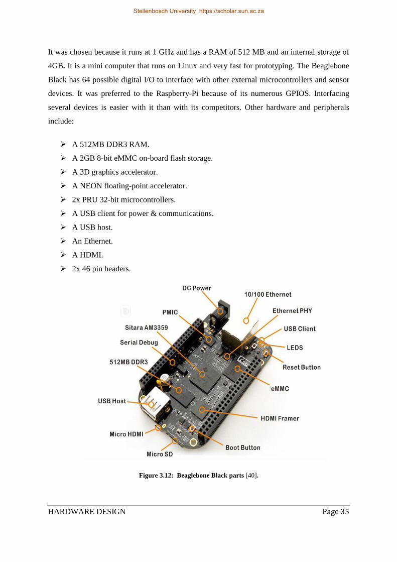
HARDWARE DESIGN Page 35
It was chosen because it runs at 1 GHz and has a RAM of 512 MB and an internal storage of
4GB. It is a mini computer that runs on Linux and very fast for prototyping. The Beaglebone
Black has 64 possible digital I/O to interface with other external microcontrollers and sensor
devices. It was preferred to the Raspberry-Pi because of its numerous GPIOS. Interfacing
several devices is easier with it than with its competitors. Other hardware and peripherals
include:
A 512MB DDR3 RAM.
A 2GB 8-bit eMMC on-board flash storage.
A 3D graphics accelerator.
A NEON floating-point accelerator.
2x PRU 32-bit microcontrollers.
A USB client for power & communications.
A USB host.
An Ethernet.
A HDMI.
2x 46 pin headers.
Figure 3.12: Beaglebone Black parts [40].
Stellenbosch University https://scholar.sun.ac.za

HARDWARE DESIGN Page 36
3.10.1 UARTS ON THE BEAGLEBONE BLACK
There are five UART ports on the Beaglebone Black. The Adafruit IO libraries make it easy
to use the UART ports. It does this by exporting the UART device tree overlays. The ground
pin for the BeagleBone Black is the first two pins of the P9 header [41]. For the project,
UART1 was used to communicate with the master greenPHY. Only the TX, RX and the
ground connection pins on the P9 header were used.
Table 3: UART on Beaglebone Black
UART RX TX CTS RTS DEVICE
UART1 P9_26 P9_24 P9_20 P9_19 /dev/tty01
UART2 P9_22 P9_21 /dev/tty02
UART3 P9_42 P8_36 P8_34 /dev/tty03
UART4 P9_11 P9_13 P8_35 P8_33 /dev/tty05
UART5 P8_38 P8_37 P8_31 P8_32 /dev/tty05
3.11 HOMEPLUG GREEN𝐏𝐇𝐘𝑻𝑴 (HPGP) MODULE
The HPGP module is at the centre of the design for this project. Its sole purpose is to enable
communication between connected devices using the power line. The home plug used for this
project is PLC Stamp 1 evaluation board from I2SE, a power line manufacturing company
based in Germany. The I2SE PLC Stamp 1 evaluation board (HPGP module) comprises a
QCA7000 (Power line chip) and the MK20DX256VMC7 microcontroller that controls all the
other operations of the module [42]. The QCA7000 is a special chip made by Qualcomm and
intercepts MME message frame from the power lines, decodes them and sends them to the
Freescale MK20DX256VMC7 microcontroller through a Serial Peripheral Interface (SPI)
[42].
The QCA7000 comes with its own embedded firmware, unlike the MK20DX256VMC7 that
requires flashing with researchers‟ custom written firmware. The time taken to send and
receive MME frames between the master HPGP module and the slave HPGP module is
3seconds by default, but for this design, it was hastened by reducing the timing component on
Stellenbosch University https://scholar.sun.ac.za
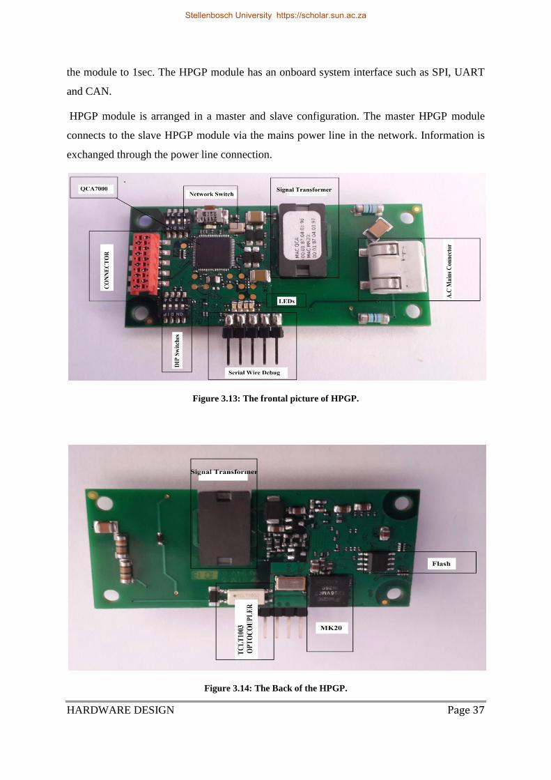
HARDWARE DESIGN Page 37
the module to 1sec. The HPGP module has an onboard system interface such as SPI, UART
and CAN.
HPGP module is arranged in a master and slave configuration. The master HPGP module
connects to the slave HPGP module via the mains power line in the network. Information is
exchanged through the power line connection.
Figure 3.13: The frontal picture of HPGP.
Figure 3.14: The Back of the HPGP.
Stellenbosch University https://scholar.sun.ac.za
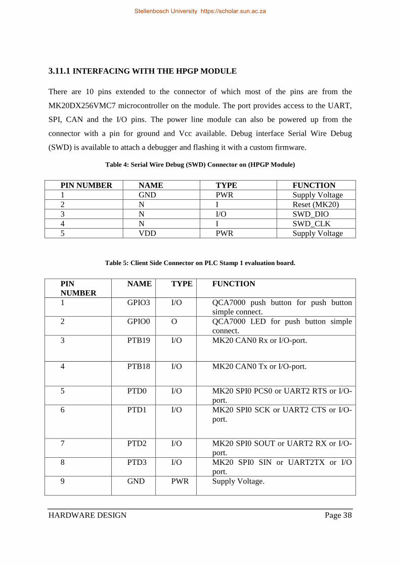
HARDWARE DESIGN Page 38
3.11.1 INTERFACING WITH THE HPGP MODULE
There are 10 pins extended to the connector of which most of the pins are from the
MK20DX256VMC7 microcontroller on the module. The port provides access to the UART,
SPI, CAN and the I/O pins. The power line module can also be powered up from the
connector with a pin for ground and Vcc available. Debug interface Serial Wire Debug
(SWD) is available to attach a debugger and flashing it with a custom firmware.
Table 4: Serial Wire Debug (SWD) Connector on (HPGP Module)
PIN NUMBER NAME TYPE FUNCTION
1 GND PWR Supply Voltage
2 N I Reset (MK20)
3 N I/O SWD_DIO
4 N I SWD_CLK
5 VDD PWR Supply Voltage
Table 5: Client Side Connector on PLC Stamp 1 evaluation board.
PIN
NUMBER
NAME TYPE FUNCTION
1 GPIO3 I/O QCA7000 push button for push button
simple connect.
2 GPIO0 O QCA7000 LED for push button simple
connect.
3 PTB19 I/O MK20 CAN0 Rx or I/O-port.
4 PTB18 I/O MK20 CAN0 Tx or I/O-port.
5 PTD0 I/O MK20 SPI0 PCS0 or UART2 RTS or I/O-
port.
6 PTD1 I/O MK20 SPI0 SCK or UART2 CTS or I/O-
port.
7 PTD2 I/O MK20 SPI0 SOUT or UART2 RX or I/O-
port.
8 PTD3 I/O MK20 SPI0 SIN or UART2TX or I/O
port.
9 GND PWR Supply Voltage.
Stellenbosch University https://scholar.sun.ac.za

HARDWARE DESIGN Page 39
10 VDD PWR Supply Voltage.
3.11.2 UART ON THE MK20DX256VMC7
The location of the UART on the PLC Stamp 1 evaluation board connector is shown in the
table below. Only the RX and TX were used in our design to save the RTS and CTS port for
other I/O connections. MK20 microcontrollers have 5 UART terminals and a USB terminal,
but one UART terminal is only directly accessible on the client connector reducing the
number of devices the HPGP module can serially communicate with.
Table 6: UART on the PLC Stamp 1 evaluation board (HPGP Module).
Pin Number Name Type Function
5 PTD0 I/O UART2_RTS
6 PTD1 I/O UART2_CTS
7 PTD2 I/O UART2_RX
8 PTD3 I/O UART2_TX
3.11.2.1 UART SETTINGS ON THE MK20DX256VMC7
The UART setting for serial communication on the HPGP module is shown in the picture
below. Interrupt is enabled for data sent serially across the embedded platforms to be reliable.
The parameters to be set are:
Baud rate: 19200 Mb/s
Parity: None
Interrupt service: Enabled
Data width: 8 bit
The transmitter and the receiver pins should be configured accordingly. By default, the port
meant for UART2 is used by CON_X3_5, CON_X3_6, CON_X3_7 and CON_X3_8 as an
I/O port. The connector pins can be configured as follows:
CON_X3_5: UART2_RTS
CON_X3_6: UART2_CTS
CON_X3_7: UART2_RX
CON_X3_8: UART_TX
Stellenbosch University https://scholar.sun.ac.za
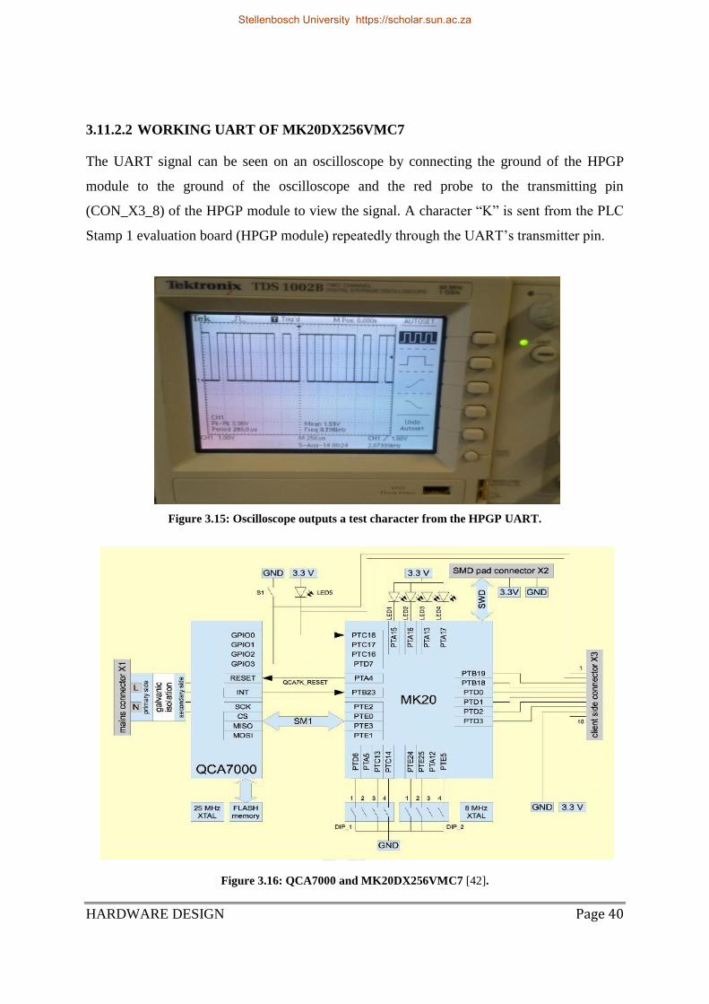
HARDWARE DESIGN Page 40
3.11.2.2 WORKING UART OF MK20DX256VMC7
The UART signal can be seen on an oscilloscope by connecting the ground of the HPGP
module to the ground of the oscilloscope and the red probe to the transmitting pin
(CON_X3_8) of the HPGP module to view the signal. A character “K” is sent from the PLC
Stamp 1 evaluation board (HPGP module) repeatedly through the UART‟s transmitter pin.
Figure 3.15: Oscilloscope outputs a test character from the HPGP UART.
Figure 3.16: QCA7000 and MK20DX256VMC7 [42].
Stellenbosch University https://scholar.sun.ac.za
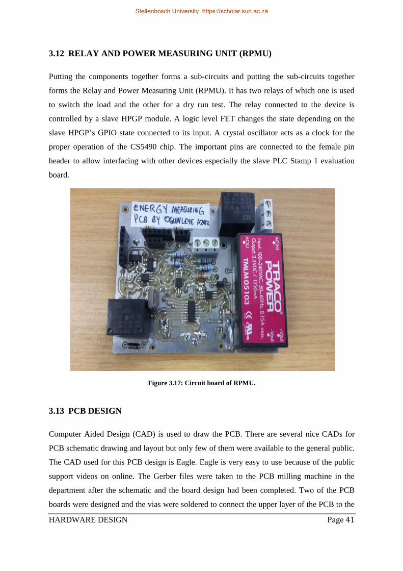
HARDWARE DESIGN Page 41
3.12 RELAY AND POWER MEASURING UNIT (RPMU)
Putting the components together forms a sub-circuits and putting the sub-circuits together
forms the Relay and Power Measuring Unit (RPMU). It has two relays of which one is used
to switch the load and the other for a dry run test. The relay connected to the device is
controlled by a slave HPGP module. A logic level FET changes the state depending on the
slave HPGP‟s GPIO state connected to its input. A crystal oscillator acts as a clock for the
proper operation of the CS5490 chip. The important pins are connected to the female pin
header to allow interfacing with other devices especially the slave PLC Stamp 1 evaluation
board.
Figure 3.17: Circuit board of RPMU.
3.13 PCB DESIGN
Computer Aided Design (CAD) is used to draw the PCB. There are several nice CADs for
PCB schematic drawing and layout but only few of them were available to the general public.
The CAD used for this PCB design is Eagle. Eagle is very easy to use because of the public
support videos on online. The Gerber files were taken to the PCB milling machine in the
department after the schematic and the board design had been completed. Two of the PCB
boards were designed and the vias were soldered to connect the upper layer of the PCB to the
Stellenbosch University https://scholar.sun.ac.za

HARDWARE DESIGN Page 42
bottom layer. Board houses would have cost more and it would have taken time to complete
the PCB from sending the Gerber to receiving the final board.
3.14 SUMMARY
This chapter explained the engineering decisions made during the design of the whole
system. A lot of factors had to be considered, like availability of components, cost,
complexity and reliability before settling on the design. The chapter discussed:
System integration of hardware units.
The design of a working energy measuring circuit using CS5490.
It demonstrates the feasibility of the designed system.
The analysis of the sub-circuits and reasons for choosing components for the PCB
and the system as a whole.
Stellenbosch University https://scholar.sun.ac.za
EMBEDDED SOFTWARE Page 43
CHAPTER 4
4 EMBEDDED SOFTWARE
Hardware alone cannot perform the necessary work without underlying software. A software
section is essential because it coordinates the relationship between the physical layer and
other higher layers on the OSI. It performs data organization, compression and
synchronization.
In this chapter, we discuss the firmware that was developed to run on the PLC Stamp1
evaluation board‟s MK20DX256VMC7 microcontroller and the software running on the
Beaglebone Black. The important functions, routines and data structures of the firmware are
broken down into a concise format to illustrate concepts. Although, a websocket and a web-
based dashboard developed for the project was implemented with programming languages
but it is discussed in the next chapter for organizational purposes.
4.1 THE MAIN PROGRAM ON THE BEAGLEBONE BLACK
The main program running on the Beaglebone Black coordinates serial communication, data-
link layer protocol handling and the websocket. It is written in Python and uses the
multithreading package to run multiple events concurrently. Implementing tornado websocket
renders the web-based UI and other programs running on the BBB unresponsive to command
without multithreading. The goal is to have serial communications that successfully share
resources with the tornado websocket in the main program running on the Beaglebone Black.
The main program must satisfy the following requirements:
A serial communication via UART with the master HPGP module and BBB.
A websocket which hosts a web-based UI, and bi-directionally pushes and collect data
using JavaScript.
A program implemented to generate packets.
A program to check the validity of received messages.
Implementing a database that stores data for testing.
Stellenbosch University https://scholar.sun.ac.za
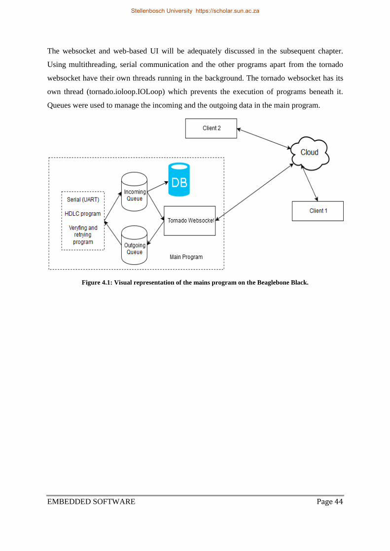
EMBEDDED SOFTWARE Page 44
The websocket and web-based UI will be adequately discussed in the subsequent chapter.
Using multithreading, serial communication and the other programs apart from the tornado
websocket have their own threads running in the background. The tornado websocket has its
own thread (tornado.ioloop.IOLoop) which prevents the execution of programs beneath it.
Queues were used to manage the incoming and the outgoing data in the main program.
Figure 4.1: Visual representation of the mains program on the Beaglebone Black.
Stellenbosch University https://scholar.sun.ac.za

EMBEDDED SOFTWARE Page 45
Figure 4.2: Beaglebone Black mains program flow diagram.
Stellenbosch University https://scholar.sun.ac.za

EMBEDDED SOFTWARE Page 46
4.2 RTOS
An Operating System (OS) of a computing platform is responsible for running applications in
a precisely timed manner, and the managing of hardware resources in a reliable and
predictable way [43]. Multitasking, Interrupts, synchronization, event handling and memory
management are all handled by the OS. A desktop OS does not suit an embedded system
application because of these following reasons:
It consumes too much space.
It is too power hungry for embedded systems i.e. Not power optimized.
It is not designed for time critical applications.
Desktop OS is not fault-tolerant and modifiable.
A Real Time Operating System (RTOS) is specifically designed to execute applications in
mostly embedded systems in a timely manner especially in applications where downtime or
delays are costly. RTOS runs on the MK20DX256VMC7 of the PLC Stamp1 evaluation
board and it performs interrupt handling and OS calls which are some of the time critical
operations to be executed [43]. Due to the increased complexity of embedded systems, RTOS
is becoming very essential to manage the numerous complex programs, device-handling and
interrupts to meet its critical time constraint avoiding disasters.
Figure 4.3: Desktop OS versus RTOS [44].
4.3 MASTER PLC STAMP1 EVALUATION BOARD
In this design, a HPGP module is designated as the master HPGP module. It sits between the
Beaglebone Black and other HPGP modules (slave HPGP modules). The master HPGP
module in conjunction with the BBB forms the command unit. It acts as a relay centre for the
Stellenbosch University https://scholar.sun.ac.za

EMBEDDED SOFTWARE Page 47
power line communication system that is an interface between Ethernet and the power line
communication. Most of the work such as framing of command and response to incoming
messages are executed by the computing platform and the slave HPGP module on the
network. If a HPGP module is hooked to a power line, it starts searching for other HPGP
modules on the network. AV Logical Network (AVLN) is only set up if there is another
device on the power line which has the same Network Membership Key (NMK) [45]. The
NMK is a string of characters that is contained in HPGP modules allowing it to participate in
an AV logical network if authenticated between the HPGP modules present on the power
line. The major work of the master HPGP module on the network is to handle UART
characters from the Beaglebone Black and copy them into the MME message frame and send
it to the appropriate slave PLC Stamp1 evaluation board on the power line. It also collects
data from the slave HPGP modules into a buffer and sends back to the Beaglebone Black via
UART.
Figure 4.4: Flow diagram of the program running in the master greenPHY.
Stellenbosch University https://scholar.sun.ac.za

EMBEDDED SOFTWARE Page 48
4.4 SLAVE PLC STAMP1 EVALUATION BOARD
The slave PLC Stamp1 evaluation board (Slave HPGP module) is responsible for receiving
data such as voltage, current and power consumed by appliances from the RPMU in the smart
grid system via its UART. It also receives instructions sent by the command unit via the
MME message frames (power line protocol) and acts on it. It stores the RPMU data into a
buffer and frame a data packet from the data received. The HDLC-like packet is sent to the
command unit as an appropriate response. The firmware running on both the master and the
slave PLC Stamp1 evaluation board are almost similar. Validation of data takes place on the
slave PLC Stamp1 evaluation board by calculating the CRC of data received and comparing
it with the CRC in the received packet to check for data corruption that may have taken place
during transmission. In the case of both the master and the slave Stamp1 evaluation board,
the buffers have to be cleared regularly after use, to allow in new data and to avoid data being
compromised due to data overflow. A unique part of the flow chart of the slave Stamp1
evaluation board is the parser that takes parameters to control the GPIO.
Figure 4.5: Flow diagram of the program running in the slave HPGP.
Stellenbosch University https://scholar.sun.ac.za

EMBEDDED SOFTWARE Page 49
4.5 RECEIVING DATA VIA MK20DX256VMC7’S UART
The process of receiving characters via the UART on the PLC Stamp1 evaluation board
(HPGP module) is interrupt driven. The advantage of using this method compared to constant
polling for data is that it saves microcontroller processing time. When the interrupts of the
HPGP modules are not set, the data set annoyingly rearranges itself at the receiver. After the
UART has being initialized, a dedicated buffer is created to store all the received characters
for processing. There are other CPU peripherals connected to the MK20DX256VMC7
microcontroller that is also interrupt driven e.g. I/O and timers. Before setting the Interrupt
flag for a process, the microcontroller checks if other interrupts especially a lower priority
Interrupt is enabled. It then disables them before executing the process. To fill up the buffer,
characters are continually checked until the End Of File is received to terminate the process.
When all the strings of characters have been received, they are stored in a buffer and used by
other resources in the microcontroller. The flag of the interrupt Rx is cleared to allow other
peripherals some CPU time. The buffer is then copied into a data buffer for use on the HPGP
module.
Figure 4.6: HPGP’s UART Rx flow chart.
Stellenbosch University https://scholar.sun.ac.za

EMBEDDED SOFTWARE Page 50
4.6 TRANSMITTING DATA VIA MK20DX256VMC7’S UART
This process is invoked if there are some data to be transmitted on the PLC Stamp 1
evaluation board‟s MK20DX256VMC7 microcontroller. Just like the Rx method, it is also
interrupt driven and has a buffer to store the string of data to be transmitted. The Tx interrupt
flag is set whenever the data to be transmitted is ready. The method continually checks that
there is no UART error (pending transmission) before proceeding to send the next available
character. The Tx interrupt flag is cleared after the last character has been sent. A prior
knowledge of the number of character bytes to be sent is essential which is accomplished by
using “byteCounter”. On the HPGP module, only one UART is configured and allowed. The
processes of UART transmission and the reception of bytes of data cannot occur
simultaneously.
Figure 4.7: HPGP’s UART TX flowchart.
Stellenbosch University https://scholar.sun.ac.za
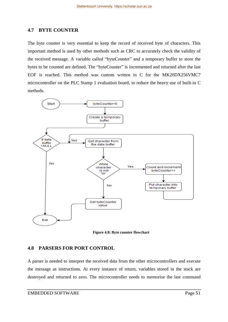
EMBEDDED SOFTWARE Page 51
4.7 BYTE COUNTER
The byte counter is very essential to keep the record of received byte of characters. This
important method is used by other methods such as CRC to accurately check the validity of
the received message. A variable called “byteCounter” and a temporary buffer to store the
bytes to be counted are defined. The “byteCounter” is incremented and returned after the last
EOF is reached. This method was custom written in C for the MK20DX256VMC7
microcontroller on the PLC Stamp 1 evaluation board, to reduce the heavy use of built-in C
methods.
Figure 4.8: Byte counter flowchart
4.8 PARSERS FOR PORT CONTROL
A parser is needed to interpret the received data from the other microcontrollers and execute
the message as instructions. At every instance of return, variables stored in the stack are
destroyed and returned to zero. The microcontroller needs to memorise the last command
Stellenbosch University https://scholar.sun.ac.za
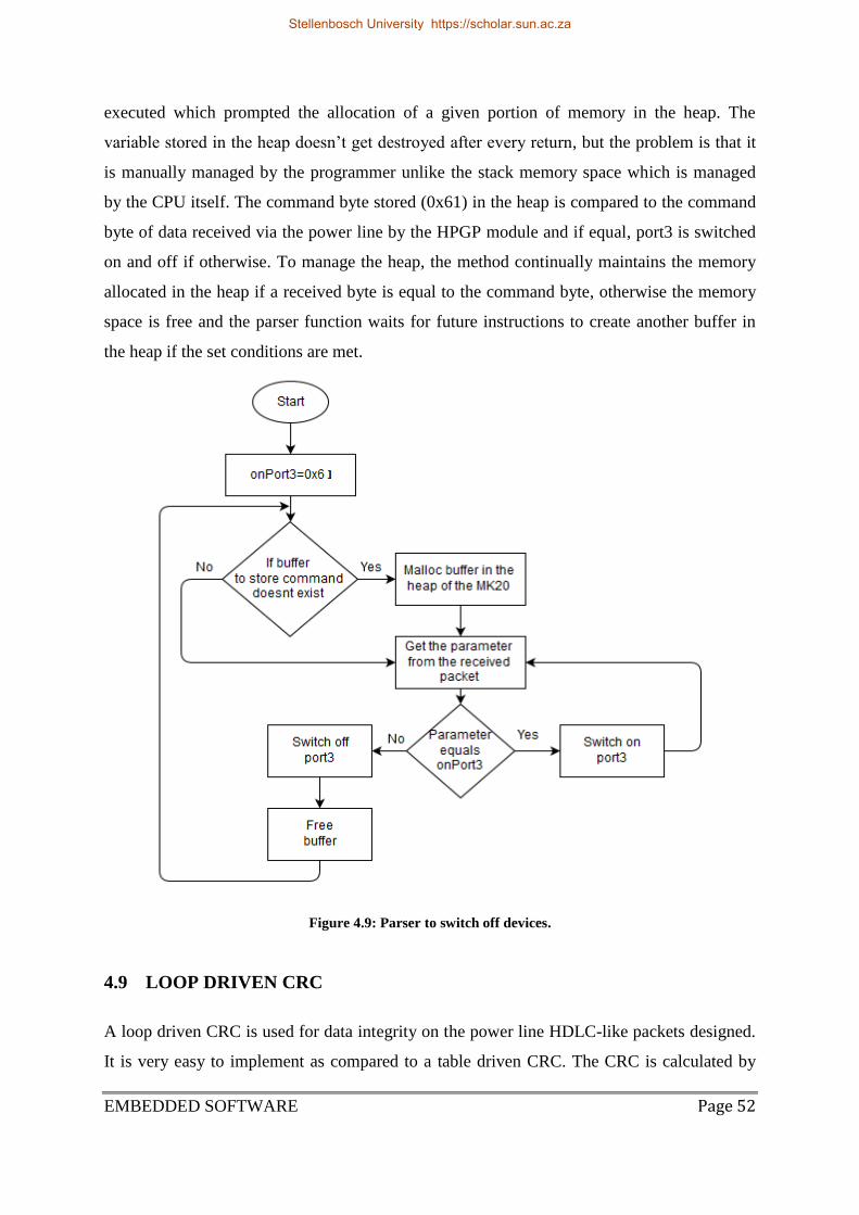
EMBEDDED SOFTWARE Page 52
executed which prompted the allocation of a given portion of memory in the heap. The
variable stored in the heap doesn‟t get destroyed after every return, but the problem is that it
is manually managed by the programmer unlike the stack memory space which is managed
by the CPU itself. The command byte stored (0x61) in the heap is compared to the command
byte of data received via the power line by the HPGP module and if equal, port3 is switched
on and off if otherwise. To manage the heap, the method continually maintains the memory
allocated in the heap if a received byte is equal to the command byte, otherwise the memory
space is free and the parser function waits for future instructions to create another buffer in
the heap if the set conditions are met.
Figure 4.9: Parser to switch off devices.
4.9 LOOP DRIVEN CRC
A loop driven CRC is used for data integrity on the power line HDLC-like packets designed.
It is very easy to implement as compared to a table driven CRC. The CRC is calculated by
Stellenbosch University https://scholar.sun.ac.za

EMBEDDED SOFTWARE Page 53
manually running its algorithm which uses more CPU cycles compared to a table driven
CRC. Each bits of the data byte is shifted into the CRC register after being XOR‟ed with the
CRC‟s most significant bit [46]. Initially, 8bit CRC was implemented for the project but was
later changed to 16bit CRC. 16bit CRC was used because it is much more robust and less
prone to error compared to 8bit CRC. CRC-CCITT was the type of the CRC used for our
design. Choosing a divisor polynomial for the CRC can be a little bit challenging but research
has shown that prime polynomials are the best [47]. The value of the CRC polynomial used is
0xA001 and an initial CRC value of 0xFFFF. The generated CRC is appended to the message
frames transmitted and received on the network. If errors are detected in a message, a NACK
frame is sent back to resend the packet.
Figure 4.10: Flow chart of the Loop Driven CRC.
Stellenbosch University https://scholar.sun.ac.za

EMBEDDED SOFTWARE Page 54
4.10 SETTING UP THE CS5490
To effectively use the CS5490 chip for energy measurement, it needs to be reset, calibrated
and setup for continuous conversion [32]. The CS5490 will automatically update and provide
new data when they are available. The CS5490 operates on a 12 bit address system [32]. The
first part of the 6 bits is for page selection and the other 6 bits determines the address on the
page [32].
4.10.1 COMMUNICATION OF CS5490
The CS5490 has a default Baud rate of 600 and the basic UART settings is a 10 bit byte
which comprises of 8 bit data, one start bit, one stop bit and no parity bits [32]. It does not
need too much configurations before use. The UART arranges bits in bytes with little
endianess i.e. Least Significant Bit (LSB) first [32], Clear to send (CTS) and Request to send
(RTS) pins which are used for flow control and are absent in CS5490 to reduce the number of
pins to be isolated by Optocoupler. The Baud rate of the chip can easily be changed by
writing to a register at address 7, Page 0 BR [15:0].
Figure 4.11: Data 8-bit byte frame.
Figure 4.12: The UART register on a CS5490 [32].
BR [15:0] = Baud Rate *524288/MCLK
The Baud rate is a determinant of the MCLK clock which is a 4.096 MHz crystal oscillator.
Stellenbosch University https://scholar.sun.ac.za

EMBEDDED SOFTWARE Page 55
4.10.2 HOST COMMANDS AND REGISTER FOR CS5490
The host command is the first byte sent to the CS5490 RX pin from the slave HPGP module.
To serially communicate with the CS5490, there are four commands to read, write registers
and instruct the calculation engine [32]. To read a register, the page select command is sent to
the RX pin of the CS5490 UART, followed by the address of the register to be read [32].
Three bytes of data are sent out of the TX pin of the UART as response to the read command
[32]. To write to a register on the CS5490, after the page has been selected, the command that
precedes it is the address write command and three bytes of data to be written to the register
address. Instruction bytes to perform specific tasks like resetting, continuous conversion and
wakeup of the CS5490 are sent as a single byte to the RX. All CS5490 operation can halt due
to sudden instruction reception. The maximum allowable time between bytes during
transmission (whether reading or writing) is 128ms before the circuit resets [32].
Figure 4.13: Reading CS5490 registers.
Figure 4.14: Diagram for writing and sending instruction to the CS5490 serially.
Stellenbosch University https://scholar.sun.ac.za

EMBEDDED SOFTWARE Page 56
Table 7: CS5490 useful commands.
Function Binary Value Note
Register Read 0 0 𝐴5 𝐴4 𝐴3 𝐴2 𝐴1 𝐴0 𝐴[5:0] specifies the register
address. Register Write 0 1 𝐴5 𝐴4 𝐴3 𝐴2 𝐴1 𝐴0
Page Select 1 0 𝑃5 𝑃4 𝑃3 𝑃2 𝑃1 𝑃0 𝑃[5:0] specifies the page.
Instruction 1 1 𝐶5 𝐶4 𝐶3 𝐶2 𝐶1 𝐶0 𝐶[5:0] specifies the instruction
4.10.3 CALIBRATION OF CS5490
The primary reasons for calibration are system noise, residual Analogy-To-Digital offset, and
component tolerances which adds some unwanted errors to the energy measuring system
[32]. The CS5490 does its calibration on board and the data are stored in its internal registers
which can be accessed by other microcontrollers via serial communication [32]. A single
calibration of the CS5490 can cater for a large range of accurate measurements of desired
instantaneous parameters like voltage, current, power and energy [32]. The calibration
calculation done and stored in the memory of the external chip (slave HPGP) which is
connected to it since it does not have a non-volatile memory onboard [32].
To calibrate, the CS5490 chip must be in an active state so that it can accurately respond to
commands [32]. The DC offset and gain calibration affects all the parameters of the CS5490
and it applies to instantaneous voltage and current unlike the AC offset calibration that affects
the RMS values. The differential signal on the pins VIN- and VIN + or IIN- and IIN+ should
be zero during the offset calculation, and no line voltage or current should be applied to the
CS5490 chip [32].
Stellenbosch University https://scholar.sun.ac.za
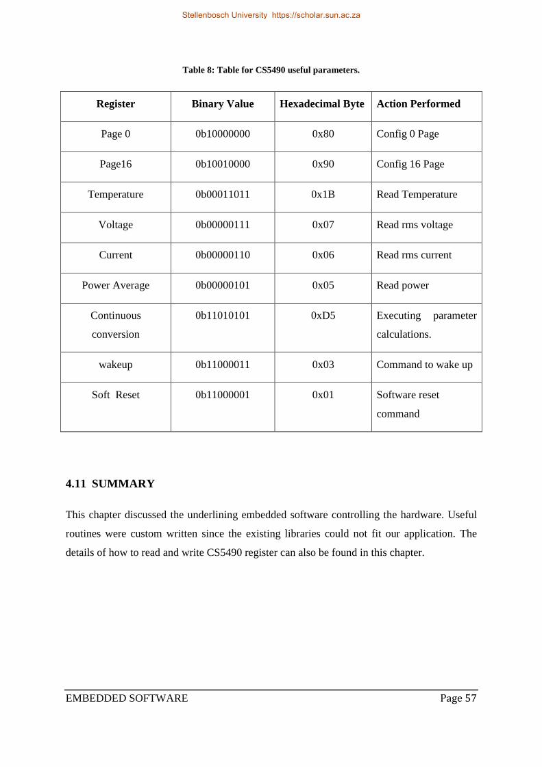
EMBEDDED SOFTWARE Page 57
Table 8: Table for CS5490 useful parameters.
Register Binary Value Hexadecimal Byte Action Performed
Page 0 0b10000000 0x80 Config 0 Page
Page16 0b10010000 0x90 Config 16 Page
Temperature 0b00011011 0x1B Read Temperature
Voltage 0b00000111 0x07 Read rms voltage
Current 0b00000110 0x06 Read rms current
Power Average 0b00000101 0x05 Read power
Continuous
conversion
0b11010101 0xD5 Executing parameter
calculations.
wakeup 0b11000011 0x03 Command to wake up
Soft Reset 0b11000001 0x01 Software reset
command
4.11 SUMMARY
This chapter discussed the underlining embedded software controlling the hardware. Useful
routines were custom written since the existing libraries could not fit our application. The
details of how to read and write CS5490 register can also be found in this chapter.
Stellenbosch University https://scholar.sun.ac.za

WEB-BASED USER INTERFACE AND DATABASE Page 58
CHAPTER 5
5 WEB-BASED USER INTERFACE AND DATABASE
Designing a web-based user interface that establishes a bi-directional communication
between a client and a server requires the abuse of Hypertext Transfer Protocol (HTTP) by
polling the server for data and at the same time sending HTTP calls. The HTTP was initially
designed for half-duplex communication in which the client makes the request and the server
prepares to respond [48]. The first web was static and not so interactive compared to dynamic
ones nowadays. Tornado webserver was a little bit cumbersome for amateur web developers
unlike the tornado websocket implementation. A lot has to be considered before designing a
web-based user interface such as:
The programming language used (Python, C#, Node.js etc).
The framework and packages (examples for python we have Tornado and web.py).
Webservers or websockets.
Synchronous or asynchronous web servers (numbers of connections to be severed at a
particular point in time).
It must have a nice look and feel.
It is imperative to be user friendly.
Initially, an interface was designed from the scratch with HTML, CSS and tornado webserver
without the functionality of a JavaScript. It resulted into a dull and not so fun web-based user
interface in figure 5.1. Connections with the webserver could be established and devices were
subsequently controlled. More than four devices could be controlled simultaneously using it
but to avoid ambiguity, it was capped to four devices. Clicking the buttons resulted into
loading different pages which was not a professional solution as compared to modern day
web pages. Data display was a big issue using this design because if its inflexibility. The
inadequacies of the interface in figure 5.1 lead to the consideration of other different
solutions. It was very clear that a solution with JavaScript is the way to go because it turned
static web pages into dynamic ones and not all operations have to be executed by the
webserver in this type of design.
Stellenbosch University https://scholar.sun.ac.za

WEB-BASED USER INTERFACE AND DATABASE Page 59
Figure 5.1: First interface.
5.1 HTML5 AND THE USER INTERFACE
HTML5 was extensively used to design the final and the other preceding web-based user
interface of this thesis. An important reason for using HTML5 is that it supports up to date
multimedia across various web browsers compared to old mark-up languages. It also
addresses the issue of combining features in HTML and XHTML together. Complex web
applications can easily be developed with it due to its rich syntax supports for Scalable
Vector Graphics contents (SVG) and different mathematical formulas.
Another advantage of HTML5 is that it supports the development of websocket applications.
HTML5 code for the interface was stored in a file named template on the Beaglebone Black
and rendered by the websocket when the URL page is visited with a browser.
5.2 CSS AND THE USER INTERFACE
Cascading Style Sheets (CSS) are used in a mark-up language such as HTML to set the look
and feel of our web-based User Interface (UI). CSS was used to create visually stimulating
user interfaces. Just like the HTML5 discussed above, CSS3 is the most recent styling
Stellenbosch University https://scholar.sun.ac.za

WEB-BASED USER INTERFACE AND DATABASE Page 60
language as of late and it was published in June 1999[49]. Although, CSS4 exists as a work
in progress and it has smaller modules than CCS 3. The CSS was stored into a file name
static on the Beaglebone Black. The path to the files was accessible to the websocket for
proper styling of the page.
5.3 JAVASCRIPT AND USER INTERFACE
It animates the static user interface designed using various scripting libraries. The gauges on
the web pages change colours and form vector depending on the values received by the
websocket. JQuery was written to allow the easy manipulation of Document Object Model
(DOM), handling of events on the client side and creating animation. The JavaScript for the
final design was stored in a file on the Beaglebone Black. The file path is accessible to
websocket for scripting functionality.
5.4 FREEBOARD.IO AND DWEET.IO
Dweet.io and Freeboard.io combines together to form a formidable, inexpensive and fast
way of getting data onto the web. It is very attractive and has a nice look and feel layout.
Dweet.io doesn‟t require any setup or registration and it is very easy to use. A Python version
of Dweet.io API was downloaded on the Beaglebone Black for use. Freeboard.io needs
registration unlike the Dweet.io but has a free version that serves the purpose of our use.
Using Dweet.io, data are sent in JSON format and are easily interpreted by Freeboard.io.
Freeboard.io display data using gauges, maps, pictures, bulbs and sparklines aggregated to
represent devices. These two free API were used to design the dashboard in figure5.2.
Freeboard.io layout deign is drag and drop.
5.4.1 DOWNSIDE OF USING DWEET.IO AND FREEBOARD.IO
The issue we had with this method is that the creator of the Freeboard.io designed it
as a dashboard that only displays data and not a complete package that allows the
client to interact with the data. Buttons were designed for it to allow full interaction
and it was not achieved due to the fact that a webserver was needed by the interface to
receive parameters from the client side.
Stellenbosch University https://scholar.sun.ac.za
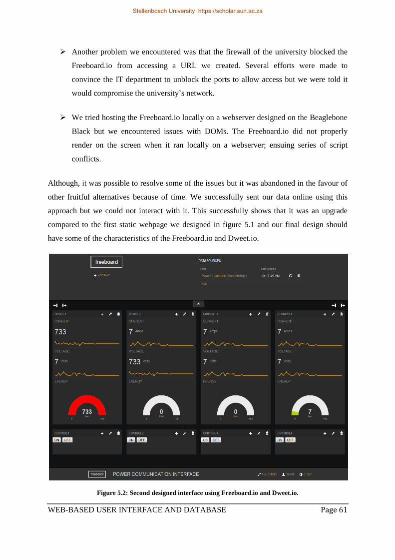
WEB-BASED USER INTERFACE AND DATABASE Page 61
Another problem we encountered was that the firewall of the university blocked the
Freeboard.io from accessing a URL we created. Several efforts were made to
convince the IT department to unblock the ports to allow access but we were told it
would compromise the university‟s network.
We tried hosting the Freeboard.io locally on a webserver designed on the Beaglebone
Black but we encountered issues with DOMs. The Freeboard.io did not properly
render on the screen when it ran locally on a webserver; ensuing series of script
conflicts.
Although, it was possible to resolve some of the issues but it was abandoned in the favour of
other fruitful alternatives because of time. We successfully sent our data online using this
approach but we could not interact with it. This successfully shows that it was an upgrade
compared to the first static webpage we designed in figure 5.1 and our final design should
have some of the characteristics of the Freeboard.io and Dweet.io.
Figure 5.2: Second designed interface using Freeboard.io and Dweet.io.
Stellenbosch University https://scholar.sun.ac.za
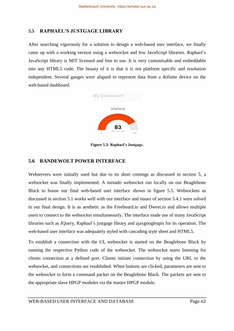
WEB-BASED USER INTERFACE AND DATABASE Page 62
5.5 RAPHAEL’S JUSTGAGE LIBRARY
After searching vigorously for a solution to design a web-based user interface, we finally
came up with a working version using a websocket and few JavaScript libraries. Raphael‟s
JavaScript library is MIT licensed and free to use. It is very customisable and embeddable
into any HTML5 code. The beauty of it is that it is not platform specific and resolution
independent. Several gauges were aligned to represent data from a definite device on the
web-based dashboard.
Figure 5.3: Raphael’s Justgage.
5.6 RANDEWOLT POWER INTERFACE
Webservers were initially used but due to its short comings as discussed in section 5, a
websocket was finally implemented. A tornado websocket run locally on our Beaglebone
Black to house our final web-based user interface shown in figure 5.5. Websockets as
discussed in section 5.1 works well with our interface and issues of section 5.4.1 were solved
in our final design. It is as aesthetic as the Freeboard.io and Dweet.io and allows multiple
users to connect to the websocket simultaneously. The interface made use of many JavaScript
libraries such as JQuery, Raphael‟s justgage library and ajaxgoogleapis for its operation. The
web-based user interface was adequately styled with cascading style sheet and HTML5.
To establish a connection with the UI, websocket is started on the Beaglebone Black by
running the respective Python code of the websocket. The websocket starts listening for
clients connection at a defined port. Clients initiate connection by using the URL to the
websocket, and connections are established. When buttons are clicked, parameters are sent to
the websocket to form a command packet on the Beaglebone Black. The packets are sent to
the appropriate slave HPGP modules via the master HPGP module.
Stellenbosch University https://scholar.sun.ac.za

WEB-BASED USER INTERFACE AND DATABASE Page 63
Figure 5.4: Client server interactions.
Figure 5.5: Final designed interface using Tornado websocket, Javascript, HTML and CSS.
Stellenbosch University https://scholar.sun.ac.za

WEB-BASED USER INTERFACE AND DATABASE Page 64
5.7 JSON
JavaScript Object Notation is a lightweight standard format of transmitting data. JSON was
used to send data from the websockets to the client-side of the web-based user interface.
Unlike XML, it is very flexible and easy to implement. All the parameters from a particular
device are stored in a JSON array and sent. Figure 5.6 taken from the web developer tools of
Firefox browser shows the JSON data. At the client-side, the parameters are accessed by
incrementing the received array element to get the next parameters.
Figure 5.6: Data in JSON format at the client-side (web-based user interface).
5.8 DATABASE
SQLite database was implemented to store data. It was chosen because of its small size, has
zero-configuration, thread-safe and embeddable. Other reasons of considering it is that it has
a Python version that seamlessly interface with the already written functional Python code of
the project. A table is created for every device connected to the power line communication
system to store their data. The data is time-stamped for future data interpretations. Although,
data on the database can be rendered on the user interface design; but was not designed in
such a way. We decided to implement the database for completeness sake because the same
data is stored in a CSV file which is a little bit easier to use.
Stellenbosch University https://scholar.sun.ac.za

WEB-BASED USER INTERFACE AND DATABASE Page 65
5.9 CSV DATA LOGGING
Apart from having a database to store data, a basic program was written to store data in a
comma separated file which serves as a quick way of interpreting data. To do this, a new
CSV file is defined on the Beaglebone Black and accessed when there is a need to log in data.
Each data set is time stamped and stored accordingly. For each of the data packets received, a
new row of information is added to the existing data.
5.10 SUMMARY
This chapter explains the effort to achieve a functional web-based user interface, the
alternative designs considered and the reasons they failed. A short section was devoted to the
database and the CSV file logging to store and analyse data. Various conditions met by the
interface are:
The ability to display data in real time.
The ability to allow users to control devices remotely from anywhere in the world.
The interface has to be aesthetic to the eyes of the clients.
Stellenbosch University https://scholar.sun.ac.za
COMMUNICATION PROTOCOL AND STRATEGY Page 66
CHAPTER 6
6 COMMUNICATION PROTOCOL AND STRATEGY
Although, it was quite clear beforehand about the communications strategy that would be
employed between various PLC modules in the power line communication system, some
quick research was done to decide the strategy that will suit the design best. At first, the
UART serial communication between the master HPGP module and the gateway had to be
sorted. A number of protocols came to mind after sorting the serial communication. It was
later agreed to implement a Modbus serial line protocol as the data-link layer for the design.
Various libraries and APIs were considered for the project but none met the design‟s
requirement. Most of the libraries were written for a general purpose computer and would be
an over kill if implemented for microcontrollers, because of their small RAM and memory.
We decided to write our own code from scratch borrowing the important part of the Modbus
Serial Line and HDLC protocol, and excluding the unnecessary part of the protocol and the
parts that would be overkill to the microcontroller. Although the Beaglebone Black could
handle the general computer version of the protocol, but such cannot be said for the
MK20DX256VMC7 microcontroller running on the PLC Stamp 1 evaluation board. The
requirements for the modified protocol are:
The Formation of packets containing a start field destination address field, command
field, data field, FCS field and CRLF.
A command packet is different compared to a response packet coming from a slave
HPGP module.
A data field that is fixed in length is used to avoid the complexities of a variable data
field.
Various destination addresses that belong to the slave node (Slave HPGP module) on
the network are defined.
ACK and NACK packets which are shorter than data and command packets created
for retries and to determine if the destination received the packet sent correctly.
The code for formation of a packet was implemented in C and it runs on the slave HPGP
module, the Python version runs on the Beaglebone Black. The structure of the packet
Stellenbosch University https://scholar.sun.ac.za

COMMUNICATION PROTOCOL AND STRATEGY Page 67
implemented in C is described below. This packet is mostly used to send command,
responses, ACK and NACK between the command unit and the slave nodes on the power
line.
typedef struct HDLC
unsigned char startHeader[3];
unsigned char addr;
unsigned char control;
unsigned char data [numbOfData];
unsigned char crc;
unsigned char *CRLF;
;
Table 9: Structure of HDLC-like packet.
Table 10: The data fields in the data packet for different events.
Frame Field Command Response ACK NACK
Starting header [0x7E, 0x7C,
0x7D]
[0x7E, 0x7C,
0x7D]
[0x7E, 0x7C,
0x7D]
[0x7E, 0x7C,
0x7D]
Address 0x30 and 0x31 0x01 0x01 0x01
Control 0x61 and !0x61
(On and Off)
0x00 0x00 0x00
Data 0x00 12 bytes of data
in Hex
“ACK” in Hex “NACK” in Hex
FCS (CRC) 2 bytes 2 bytes 2 bytes 2 bytes
Ending flag CRLF CRLF CRLF CRLF
Stellenbosch University https://scholar.sun.ac.za
COMMUNICATION PROTOCOL AND STRATEGY Page 68
The FCS and the Ending flag is explicit enough; so no explanation is required as compared to
other frame field which needs further explanation. When carriage return and line feed
(CRLF) is received, it means the packet has ended. To calculate the CRC, three frame fields,
the address, control, and data hexadecimal values are collected into a buffer and parsed
through the CRC algorithm to generate the 16-bit CRC.
6.1 STARTING HEADER
One byte header of 0x7E was initially implemented but to avoid false triggering at the
reception, we added two other bytes. The sequence of the header of which 0x7E is the first
followed by 0x7C and 0x7D is tested to validate the received message. If the sequence is not
matched, the packet is discarded. It serves as another form of validation apart from the CRC
in the message.
6.2 HPGP ADDRESSING
The master HPGP module address is denoted as 0x01 while the two slave HPGP modules are
noted as 0x30 and 0x31 for the HDLC-like protocol. The 1-byte address can support (28 -1 =
255) 255 slave HPGP module nodes because 0x01 is reserved for the master HPGP module
address. The HPGP modules have their own specific MAC address on the I2SE MME frame.
We set the destination MAC address of the master HPGP module as a broadcast
(FF:FF:FF:FF) so that it can communicate with all slave HPGP modules on the power line
network. The slave HPGP module‟s destination MAC address is the MAC address of the
master HPGP module. This prevents the slave to slave communication on the power line. The
MAC address of the HPGP modules could only have been used but for simplicity reasons, we
gave it the 1-byte address on the HDLC-like packet we developed. The packet is
encapsulated with the MME data frame for the PLC transmission.
6.3 CONTROL
The control of modules on the power line is restricted to the command unit. When an
On_button is clicked, the control field of the frame formed is set to 0x61. For the Off_button,
we are permitted to use any other hexadecimal different from 0x61which will still execute
Stellenbosch University https://scholar.sun.ac.za

COMMUNICATION PROTOCOL AND STRATEGY Page 69
properly but 0x62 was used to avoid ambiguity. The control field on the slave nodes was set
to 0x00 for completeness sake.
6.4 DATA FIELD
For a command packet, the data field is just 1byte and contains 0x00 which denotes null. The
ACK frame contains the hexadecimal representation of “ACK” and same goes for NACK.
For the data response packet, the data field contains 11 bytes of data. The 11 bytes are three
bytes for power, voltage, current and two bytes of data for temperature from the RPMU. The
command packet is the smallest possible packet followed by ACK and NACK. ACK is 1byte
smaller than the NACK packet because of “N”. Response packet is the largest with 19 bytes
in total.
6.5 NETWORK TOPOLOGY
Network topology refers to series of ways in which networks can be established between
computers. This can be physical or logical in nature. Various topologies were reviewed for
the network to be about to be set up. Some topologies were not achievable on the power lines
compared to others. Point-to-point and bus topology are the most practicable because of the
inherent nature of the power lines. Slave HPGP module are not allowed to communicate with
other slave HPGP module on the topology.
Figure 6.1: Various existing network structure [online].
Stellenbosch University https://scholar.sun.ac.za

COMMUNICATION PROTOCOL AND STRATEGY Page 70
6.5.1 POINT-TO-POINT TOPOLOGY
A point-to-point topology is very easy to implement on the power line. The communication
system will only contain two participants, the command unit (BBB and master HPGP
module) and a slave HPGP module. Collision does not happen on this type of topology,
because there is no node on the power line. During testing, a point-to-point protocol was
implemented to practically analyse the characteristics of the system without collision. In
reality, we are going to have more slave HPGP modules connected to devices in a home
environment which leads to having a bus topology.
Figure 6.2: Point-to-point connection of one master and one slave greenPHY.
6.5.2 BUS TOPOLOGY
The HPGP modules were connected to the mains on the same phase and together form a bus
topology. The bus consists of two parallel wires, the live and the neutral which serves as the
medium of transmission. The master HPGP module in conjunction with the BBB forms the
Stellenbosch University https://scholar.sun.ac.za

COMMUNICATION PROTOCOL AND STRATEGY Page 71
command unit that transmits instructions to the slave HPGP modules on the topology.
CSMA/CD is best implemented on this type of topology to avoid collision of frames. The
disadvantage of this type of topology is that if the HPGP modules are not on the same phase,
communication will fail. In figure 6.3, the RPMU and appliance section is omitted for
convenience sake. Bus topology conserves wire as compared to other topology and it is very
easy to add new nodes for expansion.
Figure 6.3: The bus topology in a home.
6.6 I2SE POWER LINE MME PROTOCOL
Transmission of data bi-directionally between the master and the slave HPGP modules entails
that some condition should be met. The MME message frame is created by copying the
Original Source Address (OSA), Original Destination Address (ODA) and other important
parameters such as MMV, MTYPE, MMTYPE, MME_SUBVER and FMI. These parameters
are essential to the receiver HPGP modules because they consist of the version and
Stellenbosch University https://scholar.sun.ac.za

COMMUNICATION PROTOCOL AND STRATEGY Page 72
characteristics of the sender. The data to be sent, if present, is also copied into the MME
frame from the data buffer.
Figure 6.4: MME data frame in relation to HDLC-like packet.
Figure 6.5: Formation of MME and data messages on the HPGP module.
Stellenbosch University https://scholar.sun.ac.za

COMMUNICATION PROTOCOL AND STRATEGY Page 73
6.7 RECEIVING DATA FROM THE POWER LINE
MME frames encapsulate the packet exchanged between two HPGP modules on the PLC
network formed. The MME messages are copied into a buffer so that it can take instructions
and data from each other. The MME message by default contains some hard coded strings of
data which are checked by the receiving HPGP module to ascertain that the actual sender can
communicate with it. The topology adopted for the design is such that only the master HPGP
module coupled with the BBB can command the slave HPGP module. After the packet has
been received, and the string matches the string in the memory of the receiver, the data buffer
is retained, else it is discarded and NACK is transmitted to the sender. Another important
condition that must also be satisfied is the length of the character received. If it is shorter than
32 bytes, that means it is incomplete and it will be discarded and NACK is sent to the sender
for retransmission. If all the conditions are adequately satisfied, the data buffer is retained and
the error checking (CRC) is performed on the bytes of data received for further validation.
Figure 6.6: Data acquisition scheme from the power line.
Stellenbosch University https://scholar.sun.ac.za

COMMUNICATION PROTOCOL AND STRATEGY Page 74
6.8 SUMMARY
Protocols and topologies are very important in communication networks. Two protocols are
discussed in this chapter, the power line MME message framing protocol from the I2SE
group and the HDLC-like protocol developed for the project. The HDLC-like packet is
encapsulated by MME frame and transported on the power lines. This section is separated
from the embedded software to give a clear view on how data are transmitted between the
nodes on the power line. Two distinct topologies exist on the PLC network, the bus topology
and the point-to-point topology.
Stellenbosch University https://scholar.sun.ac.za

TESTING AND MEASUREMENT Page 75
CHAPTER 7
7 TESTING AND MEASUREMENT
7.1 EXPERIMENTAL SETUP
For measurement, the command unit and slave HPGP modules are connected in a point-to-
point or a bus topology on the power line. An isolating transformer and a DSO-X 2002A
oscilloscope are also used for the measurements. A spectrum analyzer would have been
preferred to the oscilloscope but none suitable for 230VAC were available. A mock test was
carried out by starting the designed power line communication system so that data is
exchanged on the power line during the testing.
Figure 7.1: The experimental setup for the testing.
Stellenbosch University https://scholar.sun.ac.za

TESTING AND MEASUREMENT Page 76
7.2 SETTING UP THE OSCILLSCOPE FOR THE TESTING
The oscilloscope used was isolated from the mains to prevent the oscilloscope ground from
creating a short circuit return part for the 220 V connected to it. A probe of 100X is used to
take measurements on the power line to prevent clipping of signals. This test was carried out
in the power electronics lab in the morning. Equipment connected to the phase contributed a
significant amount of noise at the particular time the experiment was carried out. An impure
sine wave was seen on the scope in time domain. There was a notable distortion threading
back and forth across the sine wave measured. The distortion will be subsequently discussed
in the next sections. Using the FFT of the DSO, a span of range 500 Hz with an offset of 0 dB
was set to view the noise affecting the mains frequency 50Hz. As show in figure 7.3, the 50
Hz mains frequency amplitude measured with the scope is -5.7 dBV. Across the power line,
other frequencies were measured at 150 Hz with amplitude of -30 dBV and 250 Hz with
amplitude of -42.9 dBV. Power line cables acts as antennas and pick up radio noise and noise
from different sources like switches and electromagnetic equipment.
Figure 7.2: The time domain measurements of the mains.
Stellenbosch University https://scholar.sun.ac.za

TESTING AND MEASUREMENT Page 77
Figure 7.3: The frequency domain measurement of the mains.
7.3 THE DISTORTION ON THE MAINS FRQUENCY
The distortion seen on the mains frequency in the time domain was zoomed in as per figure
7.4 and further zoomed as per figure 7.5. It was discovered that the distortion consist of
varying frequencies in which the band contain frequencies between 1 MHz to about 30 MHz.
The initially thought distortions has HPGP frequencies and other noises on the power line.
FFT was used to view the frequency components of the HPGP frequency band by setting the
span of the oscilloscope to 50 MHz and the mid frequency to 25 MHz. HPGP module
operates at a frequency between 1 MHz to 30 MHz and it uses a modulating technique called
QPSK. Sub-carrier frequencies of the HPGP can be seen as shown in figure 7.6. It vanishes
and reappears on the scope in less than every 2 s. The scope at that configuration exhibits
some lags due to the fact that 2G samples were processed every second. The measured
maximum amplitude for the noise floor at the span of 50 MHz is between -70.0 dBV and -
80.1 dBV. The HPGP has an amplitude of between -21.4 dBV and -36.5 dBV during
transmission, which is at 20 dBV.
Stellenbosch University https://scholar.sun.ac.za
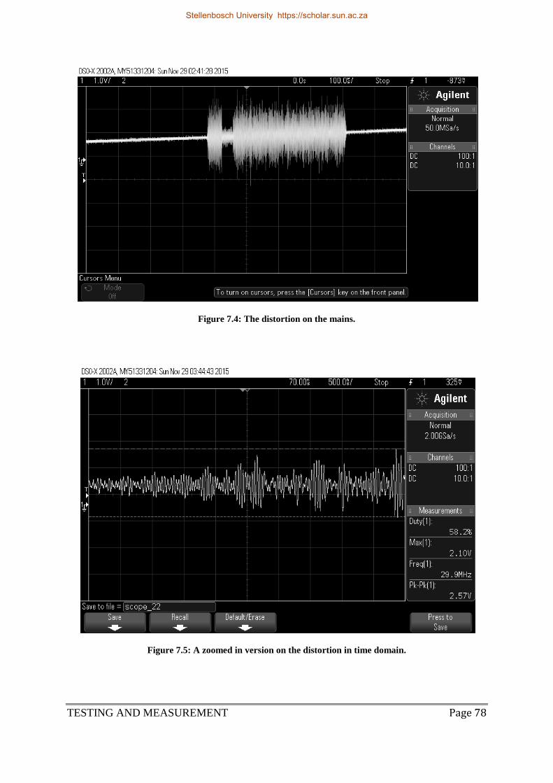
TESTING AND MEASUREMENT Page 78
Figure 7.4: The distortion on the mains.
Figure 7.5: A zoomed in version on the distortion in time domain.
Stellenbosch University https://scholar.sun.ac.za

TESTING AND MEASUREMENT Page 79
Figure 7.6: The frequency domain shows the sub-carriers of a HPGP.
7.4 ERROR PER DISTANCE WITH ONE HPGP SLAVE
For this experiment, a point-to-point topology between a slave HPGP module and the master
HPGP module was set up. 50,000 packets were sent on the power line network with varying
distances on a dead wire and on a live wire. A Python code was written to test for the
correctness of the received CRC when packets are received on the Beaglebone Black. The
packet received were time stamped and stored in a CSV file for analysis. The CSV file is
stored on the Beaglebone Black and it takes more than 12hrs for every test point to transmit
the 50,000 packets. For a particular distance, the test was carried out three times and the
average the errors obtained from the test were used in analysis. A table setup of 20cm
distance between the master HPGP module and the slave HPGP module was the first test
carried out. It was followed by separating the master and the slave HPGP module with a
distance of 5m and 17m respectively. A cable of distance 5m and 17m are used for this
separation.
Stellenbosch University https://scholar.sun.ac.za
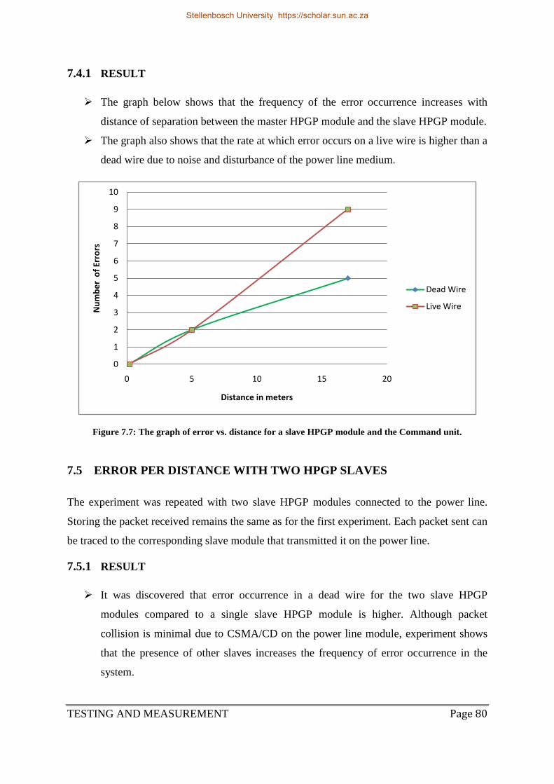
TESTING AND MEASUREMENT Page 80
7.4.1 RESULT
The graph below shows that the frequency of the error occurrence increases with
distance of separation between the master HPGP module and the slave HPGP module.
The graph also shows that the rate at which error occurs on a live wire is higher than a
dead wire due to noise and disturbance of the power line medium.
Figure 7.7: The graph of error vs. distance for a slave HPGP module and the Command unit.
7.5 ERROR PER DISTANCE WITH TWO HPGP SLAVES
The experiment was repeated with two slave HPGP modules connected to the power line.
Storing the packet received remains the same as for the first experiment. Each packet sent can
be traced to the corresponding slave module that transmitted it on the power line.
7.5.1 RESULT
It was discovered that error occurrence in a dead wire for the two slave HPGP
modules compared to a single slave HPGP module is higher. Although packet
collision is minimal due to CSMA/CD on the power line module, experiment shows
that the presence of other slaves increases the frequency of error occurrence in the
system.
0
1
2
3
4
5
6
7
8
9
10
0 5 10 15 20
Nu
mb
er
of
Erro
rs
Distance in meters
Dead Wire
Live Wire
Stellenbosch University https://scholar.sun.ac.za

TESTING AND MEASUREMENT Page 81
For the live wire, error occurrence increased further but it is still very robust for
power line communication setup. 15 bad packets occurred in 50,000 sent packets.
Figure 7.8: Error vs distance for two slave HPGP module and the command unit.
7.6 TIMING OF THE PACKET SENT ON A POWER LINE
COMMUNICATION NETWORK
Using the time package in Python, the round time trip of the packet sent from the websocket
to the slave HPGP module via the master HPGP module was measured and recorded for
analysis. A time is set when a packet is immediately created and sent. This represents the start
time and another time is set when an ACK packet is received which represents the stop time.
The difference in the start time and the stop time gives the round trip time. The system was
tested with a master HPGP module communicating with a slave HPGP module on the power
line system, scaling down disturbances to the barest minimum because of simplicity and to
benchmark the system. Various varying times were recorded during each test.
For a unit test, the web-based dashboard button was clicked to send a parameter to the
websocket which in turn generated a packet frame of 10 bytes containing the address field,
command field, end and start byte and a 16-bit (2 byte) CRC. The packet is sent from the
command unit to the slave HPGP module. At the slave HPGP module, the packet is stripped
0
2
4
6
8
10
12
14
16
0 5 10 15 20
Nu
mb
ers
of
err
ors
Distance in meters
Dead Wire
Live Wire
Stellenbosch University https://scholar.sun.ac.za

TESTING AND MEASUREMENT Page 82
down and parsed to respond to the command it received. CRC is also generated and
compared to the received packet CRC on the slave HPGP module to test the reliability and
validity. The snippet of the test in figure 7.9 shows the CRC, the frame transmitted, the
received round trip time and the ACK received from the slave HPGP module.
Figure 7.9: Snippet of packet test result from PUTTY.
Fewer data were analysed for the packet transmission, and it shows that it does not follow a
definite pattern. The mean time of the round trip generated for the packet sent is 0.76745sec.
Fast times were recorded in the data captured during the testing, but the variation in data
seems reasonable across the board. 70% of the packet round-trip time fell under 1sec.
The round trip time of a packet depends on a lot of factors such as:
The Baud rate of the serial communication.
The band width of the medium i.e the power line.
The internal delays specifically introduced by the programmer in the code.
The length of the packet (we used a fixed length of packet of size 10bytes).
Noise is not 100 percent avoidable.
7.7 CALCULATING THE DELAY THEORETICALLY
The estimated speed of the system and artificial delays introduced in the firmware code is
considered in the calculation. For serial communication (UART), the Baud rate between the
Beaglebone black and the Master HPGP module is set at 19200 Baud. On the power lines, as
reported by I2SE group, the greenPHYs can communicate at a speed of 10 Mb/s which is a
bit faster than the UART Baud rate implemented.
The UART is set at 8 bit, 1 start bit, 1 stop bit and no parity, gives 10 bits for every byte
transmitted on the UART.
Stellenbosch University https://scholar.sun.ac.za

TESTING AND MEASUREMENT Page 83
Since the Baud rate is 19200 Baud,
Number of bits per byte= 10 bits,
Time =?
𝐵𝑎𝑢𝑑 𝑟𝑎𝑡𝑒 =Number of bits per byte
time
𝑇𝑖𝑚𝑒 =Number of bits per byte
Baud rate
Time = 10
19200 = 5.2 × 10⁻⁴
Time = 0.52 ms
The calculated time is the time it takes for the UART to read and write characters across the
serial port. To get the estimated time for read and write for the UART, we multiply the time
calculated by two. Let us represent the UART time as 𝑇𝑆𝑒𝑟 , 𝑇𝑆𝑒𝑟 =2*0.52 ms
By default, the HPGP modules used in the design exchanges data with the other HPGP
modules at 3 sec intervals. The factory default was not convenient for the high speed
communication and was reduced to 500 ms to fit the purpose of the design. Further reduction
of this time causes the communication system to break and to be non-responsive at the power
line stage. The most practical time for the HPGP modules to communicate is represented here
as 𝑇𝑃𝐻𝑌 and 𝑇𝑃𝐻𝑌=500 ms. In the firmware running on the HPGP module, other artificial
delays were implemented for processing and stashing of data in buffers. The delay here is
0.1ms. We represent the delay as 𝑇𝐵𝑢𝑓 . On the Beaglebone Black, the Python code used for
the serial communication also has a delay of about 0.1 s which translates to 100 ms. The
Beaglebone Black sleeps shortly after sending a packet out, and wakes to read data
immediately after the data is available in the serial buffer. We can term the time delay as
𝑇𝐵𝑒𝑔 .
The total estimated time for delay via calculation is:
𝑇𝐸𝑠𝑡 = 𝑇𝑆𝑒𝑟 + 𝑇𝑃𝐻𝑌 + 𝑇𝐵𝑢𝑓 + 𝑇𝐵𝑒𝑔
𝑇𝑆𝑒𝑟 = 2*0.52 ms
Stellenbosch University https://scholar.sun.ac.za

TESTING AND MEASUREMENT Page 84
𝑇𝑃𝐻𝑌 = 500ms
𝑇𝐵𝑢𝑓 = 0.1ms
𝑇𝐵𝑒𝑔 = 100ms
𝑇𝐸𝑠𝑡 Not given
𝑇𝐸𝑠𝑡 = 0.52 + 500 +0.1 +100 = 601.14milsec
𝑇𝐸𝑠𝑡 = 0.601sec
0.601sec is the fastest achievable round trip time for a packet sent without noise on the
system. Round trip times much higher than the calculated time were recorded.
Figure 7.10: Arrival time for 40 packets.
0
0.2
0.4
0.6
0.8
1
1.2
1.4
0 10 20 30 40 50
Tim
e
Packet I.D
Measured Time
Calculated Time
Stellenbosch University https://scholar.sun.ac.za

TESTING AND MEASUREMENT Page 85
Beaglebone Black
Slave greenPHY
Master greenPHY
Relay and Power
Measuring Unit
Communication System on Power line
RX TX
Power lines
RX TX
HPGP speed 10Mb/s
UART Serial Protocol
at 600Baud
UART Serial Protocol
at 19200Baud
Figure 7.11: Communication system on the Power line.
7.8 SUMMARY
The results in this chapter show how various frequencies on the power line including noise
affects the power line communication system. The HPGP sub-carriers frequencies relative to
the background noise could also be seen. Error versus distance and the latency of the system
are also measured and compared with calculations.
Stellenbosch University https://scholar.sun.ac.za

CONCLUSION AND RECOMENDATIONS Page 86
CHAPTER 8
8 CONCLUSION AND RECOMENDATIONS
This thesis has presented the design of a viable power line communication system using an
HPGP module and the design of an inexpensive web-based UI for data presentation. It meets
the required expectations and it is a very attractive way of home automation compared to
various existing methods because it is inexpensive to build and robust to noise disturbances
on the power line.
8.1 SUMMARY
This project was used in HAN, but can be extended to offices and factories to control their
equipment. Chapter one discussed the important considerations to put in place before a
successful power line communication system can be designed. Chapter two described the
underlining theory and literature review of the project. The history of power line
communication and other different technologies used for smart grid technologies were also
reviewed. Various factors that mitigates against the smooth transmission of data in a power
line communication system were discussed. Chapter three of this thesis discussed the design
of embedded system hardware for the communication system. The hardware include: a
Beaglebone Black, I2SE Home Plug HPGP module and the Relay and Power Measuring Unit
(RPMU). Chapter four discussed the embedded program written for the Beaglebone Black
and the HPGP module. Chapter five discussed the functional website designed with a nice
look and feel to display data and serve as a control to the PLC system. Data were formatted in
JSON and sent to the web-based dash board. Multiple clients can connect and interact with
the web-based user interface. In chapter six, communication strategies used for the HPGP
communication and the I2SE MME protocol were discussed. Chapter seven, records the
testing of the system against noise disturbance on the PLC. The latency for data transmission
in the system was measured.
Stellenbosch University https://scholar.sun.ac.za

CONCLUSION AND RECOMENDATIONS Page 87
8.2 CONTRIBUTIONS ITO PRACTICAL FEASIBILITY
In this thesis, it was shown that an inexpensive web-based User Interface can be
developed to control many technological processes using free libraries and API.
A simple and robust communication protocol was written for the packet framing and
transmission in a power line communication system.
8.3 RECOMMENDATION
The communication system was perfectly functional and responsive to command, but some
difficulties and certain possible improvements and optimizations were identified during the
project.
8.3.1 FIREWALL
The web-based User Interface would have been easily implemented with Dweet.io and
Freeboard.io if not for the university‟s firewall blocking the ports from responding to external
request. Efforts were made to get the IT department open up a port for easy communication
with the Freeboard.io but permission was refused. An easy solution is not possible, due to the
possibility of attack by malicious hackers if the port was opened to external sources.
8.3.2 MK20DX256VMC7
The Freescale ARM microcontroller on the PLC Stamp 1 evaluation board in conjunction
with code warrior was challenging to use. Solution to this challenge is to purchase the energy
I.C QCA7000 separately, and utilizing it with an easy to use microcontroller such as ATMEL
building a power line module.
8.3.3 HPGP MODULE
The I2SE PLC Stamp 1 evaluation board used has a fewer extended ports from the
MK20DX256VMC7 microcontroller. It was possible to control two devices at a time on the
HPGP module, but the downside is that it only has one serial port to send data. The solution
to this problem would be to design the power line communication module by using different
parts e.g QCA7000 I.C, combined with other powerful microcontrollers to mitigate against
the disadvantages.
Stellenbosch University https://scholar.sun.ac.za

CONCLUSION AND RECOMENDATIONS Page 88
8.3.4 PCB DESIGN
The RRPMU PCB used for the project was designed in-house. The down side of this is that
the vias are not coated to join the top and bottom layer of the board together resulting to
joining them with a wire. The solution to these challenges is to design the PCB using CAD
e.g. Eagle, and send the Gerber files to an appropriate board house for the PCB manufacture.
8.3.5 PHASE
For a proper power line network, the power modules must be on the same phase for
communication. This was a problem experienced during testing due to the fact that sockets in
the lab were on different phases. We called in the technician that knows how the lab was
wired but at the end of the day, it resulted to guess work and time waste. A custom built test
setup would greatly enhance future testing procedure.
Stellenbosch University https://scholar.sun.ac.za

REFERENCES Page 89
REFERENCES
[1] Western Australia Office of Energy Government of, “Demand Management,” Off.
Energy, 2010.
[2] S. Thuletho Zwane, “Eskom: Majuba coal silo collapse has „significant
consequences,‟” Mail& Guardian. [Online]. Available: http://mg.co.za/article/2014-
11-03-eskom-majuba-collapse-has-significant-consequences. [Accessed: 06-Dec-
2015].
[3] G. van der Nest, “The economic consequences of load shedding in South Africa and
the state of the electrical grid,” tralac. [Online]. Available:
http://www.tralac.org/discussions/article/7000-the-economic-consequences-of-load-
shedding-in-south-africa-and-the-state-of-the-electrical-grid.html. [Accessed: 06-Dec-
2015].
[4] W.-Y. C. H. ;H. V. P. Sun, “Energy Imbalance Management Using a Robust Pricing
Scheme,” IEEE Trans. Smart Grid, vol. vol.4, no. no.2, pp. pp.896–904.
[5] A. Shepherd, “Performance of Power Line Communication with IDMA Schemes,”
M.Tech, H.B.T.I Kanpur, India, no. 5904530009.
[6] S. Venkatesulu, L. Hemasundar, M. Sreeja, K. Divya, G. J. Kumar, and M.
Bhogendranadh, “Data Transmission and Reception using Power Line
Communication,” Int. J. Res. Avent Technol., vol. 2, no. 4, pp. 250–255, 2014.
[7] W. Chiu, H. Sun, and H. V. Poor, “Using a Robust Pricing Scheme,” IEEE Trans.
Smart Grid, vol. 4, no. 2, pp. 896–904, 2013.
[8] Kashmir Hill, “When „Smart Homes‟ Get Hacked: I Haunted A Complete Stranger‟s
House Via The Internet.” [Online]. Available:
http://www.forbes.com/forbes/welcome/.
[9] H. P. Alliance, “The Standard for In-Home Smart Grid Powerline Communications :
An application and technology overview Home Plug Green PHY TM
1 . 1 The Standard
for Smart Grid Powerline Communications,” no. October, pp. 1–17, 2012.
[10] S. Katar, L. Yonge, R. Newman, and H. a Latchman, “Efficient framing and ARQ for
high-speed PLC systems,” Power Line Commun. Its Appl. 2005 Int. Symp., pp. 27–31,
Stellenbosch University https://scholar.sun.ac.za

REFERENCES Page 90
2005.
[11] R. Newman, L. Yonge, S. Gavette, and R. Anderson, “HomePlug AV Security
Mechanisms,” Power Line Commun. Its Appl. 2007. ISPLC ’07. IEEE Int. Symp., pp.
366–371, 2007.
[12] Alliance HPGP, “HomePlug TM
AV2 Technology,” HomePlug Powerline Alliance,
Inc, 2013.
[13] ARIVUS IAd, “OFDM Based High Speed Narrowband PLC Approved for Smart
Metering and Smart Grids,” ARIVUS IAd, 2009.
[14] M. R. and K. D. M. Gotz, “Power line channel characteris- tics and their effect on
communication system design,” IEEE Commun Mag., vol. April, 200, no. issue 4, p.
page 78–86.
[15] Vishnu, “Modulation & Autocorrelation Techniques,” iTNOtesin. [Online]. Available:
http://itnotes.in/modulation-techniques/. [Accessed: 24-Dec-2015].
[16] E. Everett and M. Wu, “Modulation Questions from Lab 1 ?,” 2013.
[17] M. Debbah, “Short introduction to OFDM,” Mob. Commun. Gr., pp. 1–11, 2004.
[18] Ferc, “Assessment of Demand Response and Advanced Metering Staff Report Federal
Energy Regulatory Commission,” Energy, vol. 74, no. 0022–3042 SB - IM, pp. 2–5,
2011.
[19] “Solar-Maxim-Smart_Grid_Communications.pdf.” [Online]. Available:
http://www.mouser.com/pdfdocs/Solar-Maxim-Smart_Grid_Communications.pdf.
[Accessed: 08-Feb-2015].
[20] “The Enhanchment of Communication Technologies and Network for Smart Grid
Application.” [Online].Available:http://arxiv.org/ftp/arxiv/papers/1403/1403.0530.pdf.
[Accessed: 08-Feb-2015].
[21] Edvard, “Smart Grid Communications Overview,” SMART GRID. [Online]. Available:
http://electrical-engineering-portal.com/smart-grid-communications-overview.
[Accessed: 24-Dec-2015].
[22] P. Sutterlin and W. Downey, “A Power Line Communication Tutorial - Challenges
and Technologies,” Echelon Corp. December 19, 2004.
Stellenbosch University https://scholar.sun.ac.za

REFERENCES Page 91
[23] H. Ferreira, H. Grové, O. Hooijen, and A. H. Vinck, “Power line communication,”
TexasInstrument Inc., pp. 706–716, 2001.
[24] R. Sobolewski and D. Ph, “The Future of Broadband Over Power Line,”
jur.rochester.edu, pp. 29–35, 2005.
[25] M. Millanta and M. M. Forti, “A Classification of the power-line voltage Disturbances
for an exhaustive description and measurment,” IEEE smart grid, pp. 332–336.
[26] I. H. Cavdar and E. Karadeniz, “Measurements of Impedance and Attenuation at
CENELEC Bands for Power Line Communications Systems,” Sensors, vol. 8, no. 12,
pp. 8027–8036, 2008.
[27] T. Maenou and M. Katayama, “Study on Signal Attenuation Characteristics in Power
Line Communications,” 2006 IEEE Int. Symp. Power Line Commun. Its Appl., pp.
217–221, 2006.
[28] Y. Fathi, T. a Kawady, A. Husein, and M. El-geziry, “Practical Issues of Power Line
Communication for,” Int. Middle East Power Syst. Conf., pp. 634–640, 2010.
[29] R. Vines, H. Trussell, K. Shuey, and J. O‟Neal, “Impedance of the Residential Power-
Distribution Circuit,” IEEE Trans. Electromagn. Compat., vol. EMC-27, no. 1, pp. 6–
12, 1985.
[30] M. Russell, C. Engineer, and P. PowerLines, “The impact of mains impedance on
power quality,” Power Qual. 2000, vol. 2000, no. 203, 2000.
[31] M. P. Sanders and R. E. Ray, “Power line carrier channel & application considerations
for transmission line relaying,” Pulsar Technol. Inc, 2009.
[32] CIRRUS, “Two Channel Energy Measurement IC,” CIRRUS Log., 2013.
[33] T. Series, “AC / DC Power Modules,” TRACO POWER, pp. 1–4, 2013.
[34] C. Data, “HRS4 ( H ) Relay,” HKE, vol. 4, pp. 4–6.
[35] T. M. Printy, “ACPL-M50L (Optocoupler) Data sheet,” AVAGO Technol., no. January,
pp. 1–16, 2008.
[36] W. Storr, “MOSFET as a Switch,” 2010. [Online]. Available: http://www.electronics-
tutorials.ws/transistor/tran_7.html. [Accessed: 30-Jun-2015].
Stellenbosch University https://scholar.sun.ac.za

REFERENCES Page 92
[37] D. Incorporated, “60V n-channel self protected enhancement mode intellifet tm
MOSFET,” ZETEX DIODES Inc., no. June, pp. 1–9, 2010.
[38] B. S. Fuses, “IEC & British Standard Fuses IEC and British Standard Fuses IEC &
British Standard Fuses Application Data for BS Low Voltage Fuses,” pp. 217–236.
[39] C. Supported, “Beagleboard.org.” [Online]. Available: http://beagleboard.org/.
[40] John Roach, “Sending Data from a BeagleBone Black to an Android Tablet.” [Online].
Available: http://johnroach.info/2014/05/10/sending-data-from-a-beaglebone-black-to-
an-android-tablet/. [Accessed: 06-Dec-2015].
[41] “UART | Setting up IO Python Library on BeagleBone Black | Adafruit Learning
System.” [Online]. Available: https://learn.adafruit.com/setting-up-io-python-library-
on-beaglebone-black/uart. [Accessed: 17-Sep-2014].
[42] S. E. G. October, “PLC-Stamp 1 (Preliminary Datasheet),” I2SE, pp. 1–14, 2013.
[43] R. Time and E. D. Systems, “Real-Time Operating Systems VxWorks in particular
What is a Real-Time Operating System ( RTOS )?,” 2012.
[44] L. Thiele, “Embedded Systems 6 . Real-Time Operating Systems,” Comput. Netw.
Lab. (Swiss Fedral Inst. Technol., pp. 1–27.
[45] M. M. Entry, “every 5 seconds the direction of a GPIO changes (without any
debouncing) the state of a input GPIO changes (without any debouncing),” pp. 1–5.
[46] T. Schmidt, “CRC Generating and Checking,” MICROCHIP Data Sheet, p. 24, 2000.
[47] P. Koopman and T. Chakravarty, “Cyclic Redundancy Code (CRC) Polynomial
Selection For Embedded Networks,” Int. Conf. Dependable Syst. Networks, 2004, pp.
1–11, 2004.
[48] R. Fielding, U. C. Irvine, and H. Frystyk, “Hypertext Transfer Protocol,” Netw. Work.
Gr., pp. 1–60, 1996.
[49] W3C, “Descriptions of all CSS specifications,” W3C. [Online]. Available:
http://www.w3.org/Style/CSS/specs. [Accessed: 11-Oct-2015].
Stellenbosch University https://scholar.sun.ac.za

APPENDIX A Page 93
Appendix A.
J-LINK
For ARM based microcontrollers, JTAG from SEGGER is the most popular device for
flashing and debugging a wide range of ARM processors. The I2SE power line
communication module used in the project has a MK20DX256VMC7 microcontroller that
coordinates the overall operation and serial communication of the module.
The J-Link EDU is used for educational purposes and may not be used by a profit
organization or business purposes.
To use J-Link with code warrior, three installations are needed.
The J-Link debugging plug-in
The GDB debugger (client) application, as part of the GNU tool chain
The SEGGER J-Link GDB server and driver.
Figure A.1: J-Link debugger
Stellenbosch University https://scholar.sun.ac.za

APPENDIX A Page 94
J-LINK COMMANDER
To verify the proper functionality of the J-Link, the user will have to navigate to “c:\Program
Files(x86)\SEGGER\JLinkARM_V445a\JLink.exe” and execute the JLink.exe. Commands
like halt, memory dump, step and go are all used to verify the target connection. Below is a
sample of results from executing JLink.exe.
Figure A.2: Shell for J-Link
To perform debugging with a debugger, two systems have to be set up, the Host System and
the Target System.
HOST SYSTEM
The host system runs a desktop operating system (windows or Linux) and provides support
to the J-Link via the USB to relate with the code warrior, eclipses or and other IDE supported
by J-Link.
Stellenbosch University https://scholar.sun.ac.za

APPENDIX A Page 95
TARGET SYSTEM
The target system comprises of the target CPU (microcontroller) and its peripherals to be
flashed and debugged. It is very important that the target CPU is supported and compatible
with the J-Link debugger.
Figure A.3: The connection between target, host and a debugger.
Stellenbosch University https://scholar.sun.ac.za

APPENDIX B Page 96
Appendix B.
CODE WARRIOR
This is a rich embedded software development studio and a complete IDE that is visually
stimulation and used to accelerate the development of complicated embedded applications. It
is an optimisation tool used to programme from entry level 8-bit microcontroller to 32-bit
complex microcontrollers. It was extensively used to programme the ARM microcontroller
on the greenPHY module. To start with code warrior, a workspace is created for the modules
that will run on it.
This is where to find the latest edition of code warrior
(http://www.freescale.com/tools/software-and-tools/software-development-tools/codewarrior-
development-tools/downloads/special-edition-software:CW_SPECIALEDITIONS)
FEATURES OF CODE WARRIOR
Classic IDE
Infinite number of assemblers
Large collection of C/C++ Compiler and Debugger and restricted based on the
version.
Flash Programmer integration.
Full Chip Simulation for RS08 and S08 chips.
Device Initialization tool
Processor Expert with basic, software and advanced components (restrictions based
on suite)
Processor Expert Component Wizard (restrictions based on suite)
OSEK kernel awareness (restrictions based on suite)
Profile analysis (restrictions based on suite)
Code coverage (restrictions based on suite)
PC-Lint plug-in (restrictions based on suite)
Stellenbosch University https://scholar.sun.ac.za

APPENDIX B Page 97
SYSTEM REQUIREMENTS FOR CODE WARRIOR TO FUNCTION PROPERLY
1.0 GHz Pentium® compatible processor or better
Microsoft Windows® XP/Vista (32-bit)
1 GB RAM
Disk Space: 2 GB total, 400 MB on Windows system disk
CD-ROM drive for installation
USB port for communications with target hardware
(optional) Ethernet port for communication with target hardware
HOST TARGET INTERFACES
Open Source BDM
Open Source JTAG
OpenSDA
CodeWarrior USB TAP
CodeWarrior Ethernet TAP
Cyclone MAX (P&E Microcomputer Systems)
Cyclone PRO (P&E Microcomputer Systems)
Cyclone Universal [FX] (P&E Microcomputer Systems)
J-Link (Segger)
J-Trace (Segger)
USB BDM Multilink (P&E Microcomputer Systems)
USB Multilink PPCNEXUS (P&E Microcomputer Systems)
USB Multilink Universal [FX] (P&E Microcomputer Systems)
Tracelink (P&E Microcomputer Systems)
Stellenbosch University https://scholar.sun.ac.za

APPENDIX C Page 98
Appendix C.
RELAY AND POWER MEASURING PCB
Figure C.1: RPMU PCB Component layout.
Figure C.2: Top layer of the RMPU PCB.
Stellenbosch University https://scholar.sun.ac.za

APPENDIX C Page 99
Figure C.3: Bottom layer of the RPMU PCB.
Stellenbosch University https://scholar.sun.ac.za

APPENDIX C Page 100
Figure C.4: Schematic of the RPMU.
Stellenbosch University https://scholar.sun.ac.za