design and applications of cmos current conveyors
TRANSCRIPT

Design and Applications ofCMOS Current Conveyors
by
David Moro Fr ıas
A DissertationSubmitted to the Program in Electronics Science,
Electronics Science Departmentin partial fulfillment of the requirements for the degree of
MASTER IN ELECTRONICS SCIENCE
at the
National Institute for Astrophysics, Optics and ElectronicsJune 2008
Tonantzintla, Puebla
Advisors:
Dr. Esteban Tlelo Cuautle, INAOEDr. Mourad Fakhfakh, ENIS
c©INAOE 2008All rights reserved
The author hereby grants to INAOE permission to reproduce andto distribute copies of this thesis document in whole or in part


Abstract
A Current Conveyor (CC) is a minimum 3-terminals device which can perform
many useful analog signal processing functions. The first generation CC was
introduced in 1969, and more recently, it is a good alternative in Current-Mode
design. Nowadays, the CCs can be classified as direct and inverted, and they are
divided as first, second and third generation, where they can be positive-type,
negative-type, multiple-output and/or current-controlled.
In this Thesis it is highlighted that the CC can be easily designed by combining
the connection among different Unity Gain Cells (UGCs) as basic building blocks.
Furthermore, from the characteristic equation of each kind of CC, they can be
implemented just by superimposing or by cascading UGCs such as voltage (VF)
and current followers (CF), and voltage (VM) and current mirrors (CM).
New Nullor equivalent representations for all CC topologies are introduced in
this work, which are used to perform symbolic analysis of CC-based circuits by
applying Nodal Analysis (NA). It is shown that the nullor is a very useful concept
that helps the designer to easily analyze analog circuits. In this manner, by using
this ideal concept, analytical equations (transfer functions) of CC-based circuits
are calculated.
The realization of the UGC-based CCs begins by designing each UGC at the
transistor level of abstraction. Each UGC has been designed as a symmetrical
type circuit in order to allow superimposing or cascading connection to implement
all kinds of CCs, both direct and inverted. Finally, some applications of the
UGC-based CCs, like filtering, sinusoidal oscillator and inductance simulator, are
presented to show their suitability and usefulness in the field of analog signal
processing.
i

Resumen
El Current Conveyor (CC) es un dispositivo con un mınimo de tres terminales,
el cual puede realizar diversas funciones de procesado analogico de senales. La
primera generacion de los CC fue presentada en 1969, y recientemente se ha visto
como una buena alternativa en el diseno de circuitos en modo corriente. Los CC
pueden ser clasificados como directos o inversos, divididos en primera, segunda y
tercera generacion, los cuales estan subdivididos en positivos, negativos, multiples
salidas y/o controlados por corriente.
En el presente trabajo los CC son disenados combinando diferentes celdas de
ganancia unitaria (UGCs) como bloques basicos de diseno. Tomando la ecuacion
caracterıstica de cada tipo de CC, estos pueden ser implementados superim-
poniendo estas UGCs, tales como los seguidores de voltaje (VF) y corriente (CF),
y espejos de voltaje (VM) y corriente (CM).
Se presentan nuevos equivalentes con nullor para todas las topologıas de CC,
los cuales son usados para realizar un analisis simbolico de circuitos basados en
CC aplicando analisis nodal (NA). Se muestra que el nullor es un concepto muy
util que ayuda al disenador a analizar facilmente circuitos analogicos. De esta
manera, utilizando este concepto ideal, se calculan las funciones de transferencia
de varios circuitos basados en los CC.
La realizacion de los CC basados en UGCs comienza disenando cada una de es-
tas celdas a nivel transistor. Las UGCs fueron disenadas como circuitos simetricos
para poder superimponer cada una de estas celdas para implementar todos los
tipos de CC, tanto directos como inversos. Finalmente, algunas aplicaciones de
estos CC basados en UGCs son implementados, tales como filtros, osciladores si-
nusoidales o simuladores de inductancias para demostrar su utilidad en el campo
iii

del proceso analogico de senales.

Acknowledgements
I want to express my sincere gratitude to:
• Dr. Esteban Tlelo Cuautle for being the director of this thesis and for all
his help during this time.
• Dr. Mourad Fakhfkah for being the co-advisor of this thesis and for his
ideas, suggestions and comments.
• Defense committee: Dr. Arturo Sarmiento Reyes, Dr. Luis Hernandez
Martınez, Dra. Ma. Teresa Sanz Pascual, Dr. Carlos Sanchez Lopez and
Dr. David Baez Lopez for their comments and suggestions.
• National Institute of Astrophysics, Optics and Electronics (INAOE) to give
me the opportunity to have studied into an institution of academic excel-
lence.
v

Contents
Abstract i
Resumen iii
Acknowledgements v
1 Introduction 1
1.1 Problem Description . . . . . . . . . . . . . . . . . . . . . . . . . 2
1.2 History... . . . . . . . . . . . . . . . . . . . . . . . . . . . . . . . . 4
1.3 Objectives . . . . . . . . . . . . . . . . . . . . . . . . . . . . . . . 5
1.4 Thesis Organization . . . . . . . . . . . . . . . . . . . . . . . . . . 6
2 Current Conveyor 7
2.1 First Generation Current Conveyor (CCI) . . . . . . . . . . . . . 8
2.1.1 Positive/Negative CCI . . . . . . . . . . . . . . . . . . . . 9
2.1.2 Direct/Inverse CCI . . . . . . . . . . . . . . . . . . . . . . 10
2.1.3 Multiple-Output CCI . . . . . . . . . . . . . . . . . . . . . 11
2.1.4 Current Controlled CCI . . . . . . . . . . . . . . . . . . . 12
2.2 Second Generation Current Conveyor (CCII) . . . . . . . . . . . . 12
2.2.1 Positive/Negative CCII . . . . . . . . . . . . . . . . . . . . 13
2.2.2 Direct/Inverse CCII . . . . . . . . . . . . . . . . . . . . . 14
2.2.3 Multiple-Output CCII . . . . . . . . . . . . . . . . . . . . 15
2.2.4 Current Controlled CCII . . . . . . . . . . . . . . . . . . . 15
2.3 Third Generation Current Conveyor (CCIII) . . . . . . . . . . . . 16
2.3.1 Positive/Negative CCIII . . . . . . . . . . . . . . . . . . . 17
vii
viii CONTENTS
2.3.2 Direct/Inverse CCIII . . . . . . . . . . . . . . . . . . . . . 17
2.3.3 Multiple-Output CCIII . . . . . . . . . . . . . . . . . . . . 18
2.3.4 Current Controlled CCIII . . . . . . . . . . . . . . . . . . 19
3 Nullor 21
3.1 Nullor Equivalents . . . . . . . . . . . . . . . . . . . . . . . . . . 22
3.2 Current Conveyor Nullor Equivalents . . . . . . . . . . . . . . . . 24
3.2.1 CCI Nullor Equivalents . . . . . . . . . . . . . . . . . . . . 26
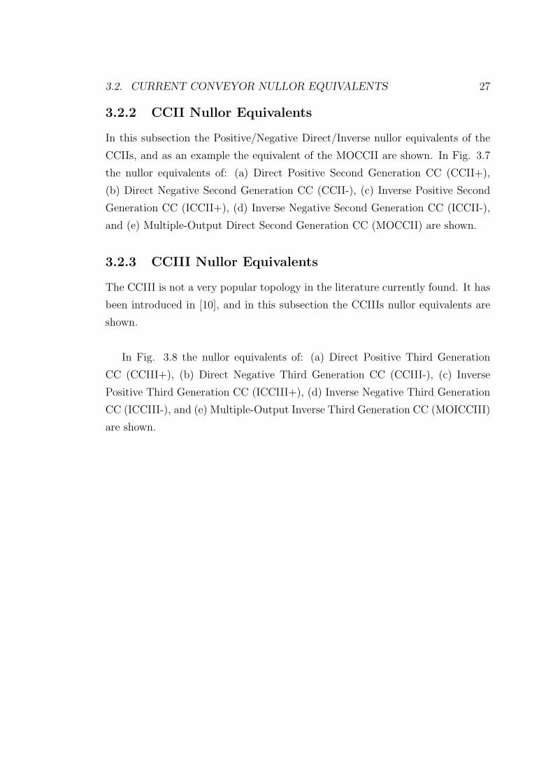
3.2.2 CCII Nullor Equivalents . . . . . . . . . . . . . . . . . . . 27
3.2.3 CCIII Nullor Equivalents . . . . . . . . . . . . . . . . . . . 27
3.3 Analysis of CC-Based Circuits . . . . . . . . . . . . . . . . . . . 30
3.3.1 Nodal Analysis (NA) . . . . . . . . . . . . . . . . . . . . . 30
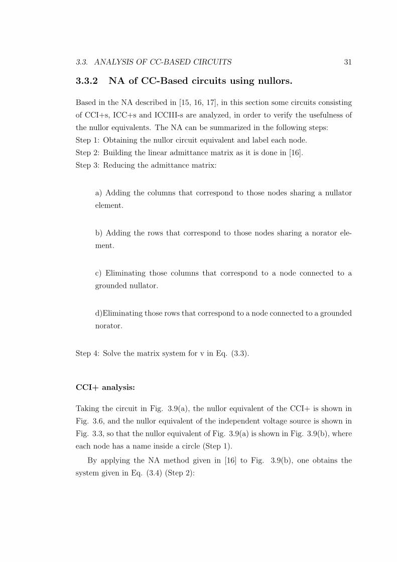
3.3.2 NA of CC-Based circuits using nullors. . . . . . . . . . . . 31
3.4 Nullor-Based Current Mode Universal Filter . . . . . . . . . . . . 41
4 Unity Gain Cells (UGCs) 45
4.1 Voltage Follower (VF) . . . . . . . . . . . . . . . . . . . . . . . . 45
4.1.1 VF-A . . . . . . . . . . . . . . . . . . . . . . . . . . . . . 46
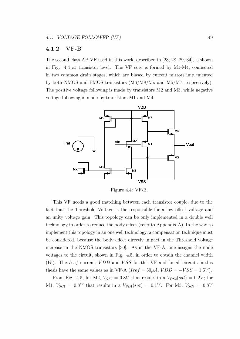
4.1.2 VF-B . . . . . . . . . . . . . . . . . . . . . . . . . . . . . . 49
4.1.3 VF-C . . . . . . . . . . . . . . . . . . . . . . . . . . . . . . 50
4.1.4 VFs Measurements . . . . . . . . . . . . . . . . . . . . . . 52
4.2 Current Mirror (CM) . . . . . . . . . . . . . . . . . . . . . . . . . 53
4.2.1 Simple CM (SCM) . . . . . . . . . . . . . . . . . . . . . . 54
4.2.2 Low Voltage CM (LVCM) . . . . . . . . . . . . . . . . . . 55
4.2.3 Cascode and Wilson CM . . . . . . . . . . . . . . . . . . . 56
4.2.4 CMs Measurements . . . . . . . . . . . . . . . . . . . . . . 57
4.3 Voltage Mirror (VM) . . . . . . . . . . . . . . . . . . . . . . . . . 58
4.3.1 VMs Measurements . . . . . . . . . . . . . . . . . . . . . . 60
4.4 Current Follower (CF) . . . . . . . . . . . . . . . . . . . . . . . . 61
4.4.1 CFs Measurements . . . . . . . . . . . . . . . . . . . . . . 61
5 Direct and Inverse Current Conveyors 63
5.1 Direct Current Conveyors . . . . . . . . . . . . . . . . . . . . . . 64
CONTENTS ix
5.1.1 Direct First Generation Current Conveyor (CCI) . . . . . 64
5.1.2 Direct Second Generation Current Conveyor (CCII) . . . . 71
5.1.3 Direct Third Generation Current Conveyor (CCIII) . . . . 77
5.2 Inverse Current Conveyors (ICCs) . . . . . . . . . . . . . . . . . . 83
5.2.1 Inverse First Generation Current Conveyor (ICCI) . . . . . 83
5.2.2 Inverse Second Generation Current Conveyor (ICCII) . . . 89
5.2.3 Inverse Third Generation Current Conveyor (ICCIII) . . . 94
5.3 Parasitic Elements . . . . . . . . . . . . . . . . . . . . . . . . . . 99
6 Applications 101
6.1 CCI Applications . . . . . . . . . . . . . . . . . . . . . . . . . . . 101
6.1.1 CCI-Based Filters . . . . . . . . . . . . . . . . . . . . . . . 101
6.1.2 Sinusoidal Oscillator . . . . . . . . . . . . . . . . . . . . . 105
6.2 CCII Applications . . . . . . . . . . . . . . . . . . . . . . . . . . . 108
6.2.1 Universal Current-Mode Filter . . . . . . . . . . . . . . . . 108
6.2.2 Floated Inductance Simulators . . . . . . . . . . . . . . . . 109
6.2.3 Four Terminal Floating Nullor (FTFN) . . . . . . . . . . . 112
6.3 ICCII Applications . . . . . . . . . . . . . . . . . . . . . . . . . . 118
6.3.1 Universal Voltage-Mode Filter . . . . . . . . . . . . . . . . 118
7 Conclusions 121
7.1 Lines of Future Work . . . . . . . . . . . . . . . . . . . . . . . . . 122
Published Papers 123
A MOS Transistor Characteristics 125
A.1 Threshold Voltage . . . . . . . . . . . . . . . . . . . . . . . . . . . 125
A.2 CMOS Transistor Regions . . . . . . . . . . . . . . . . . . . . . . 127
A.3 Second-Order Effects . . . . . . . . . . . . . . . . . . . . . . . . . 132
A.3.1 Body Effect . . . . . . . . . . . . . . . . . . . . . . . . . . 132
A.3.2 Channel Modulation Effect . . . . . . . . . . . . . . . . . . 133
B CCs transistor level topologies 137
B.1 CCs . . . . . . . . . . . . . . . . . . . . . . . . . . . . . . . . . . 137
x CONTENTS
B.1.1 CCIs . . . . . . . . . . . . . . . . . . . . . . . . . . . . . . 137
B.1.2 CCIIs . . . . . . . . . . . . . . . . . . . . . . . . . . . . . 141
B.1.3 CCIIIs . . . . . . . . . . . . . . . . . . . . . . . . . . . . . 144
B.2 ICCs . . . . . . . . . . . . . . . . . . . . . . . . . . . . . . . . . . 147
B.2.1 ICCIs . . . . . . . . . . . . . . . . . . . . . . . . . . . . . 147
B.2.2 ICCIIs . . . . . . . . . . . . . . . . . . . . . . . . . . . . . 150
B.2.3 ICCIIIs . . . . . . . . . . . . . . . . . . . . . . . . . . . . 153

Chapter 1
Introduction
Since the introduction of integrated circuits, the operational amplifier (opamp)
has been the basic analog building block in circuit design, it has been evolved by
introducing new analog integrated circuit applications and by changing the analog
circuit requirements [1].
Early high-gain amplifiers were implemented using discrete thermionic valves
which were inherently voltage-controlled devices with controlled voltage output al-
lowed stages to be easily cascaded. Then the resulting voltage opamp architectures
were translated to silicon with the development of integrated circuit technologies,
and this device become ubiquitous to the area of analog signal processing [2].
The opamp has several attractive features, such as the differential pair input
stage that is very good in rejecting common-mode signals. Moreover, this device
only requires a single-ended output to provide a negative feedback and to drive a
load, and its implementation is simpler than a fully differential or balanced output.
But on the other side, it has negative issues, as its architecture that produces
certain inherent limitations in both performance and versatility. The first one is
limited by a fixed gain-bandwidth product and a slew rate whose maximum value
is determined by the input stage bias current. The second one is constrained by
the single-ended output, since the device cannot be easily configured in closed-loop
to provide a controlled output current, because it is used for the implementation
of closed-loop voltage-mode circuits [2].
Also, the performance of analog systems degrades because small size devices
1
2 CHAPTER 1. INTRODUCTION
cannot be used due to noise and off-set constraints. Often, low voltage operation
leads to complex circuits with degraded performance, forcing the analogue design-
ers to look for new circuit architectures. Toward this end, current-mode design
techniques offer voltage independent and high performance analogue circuits like
Current Conveyors (CCs) [3].
Due to these drawbacks, when low power consumption with low voltage op-
eration and a large bandwidth are required, opamp-based circuits become too
complex. An alternative for the realization of these voltage-mode circuits is to
use current signals rather than voltage signals in signal processing circuits [4].
In current-mode design, MOS transistors are more suitable for processing cur-
rent than voltage signals, because the output of this type of transistors is current,
both in common-source and common-gate amplifier configurations. Common-
drain amplifier configuration is useless at low supply voltages because its bulk-
effect. A common application in current-mode for the MOS-transistors are the
Current Mirrors, which are more accurate and less sensitive to process variations
than those Current Mirrors based in bipolar transistors, because with the latter
the base currents limit the accuracy of the circuit [1].
Current-mode circuits have some recognised advantages: They do not require
a high voltage gain, so high performance amplifiers are not required. They do not
need high precision passive components, so they can be designed almost entirely
with transistors, making these circuits compatible with typical digital processes.
And as mentionated before, they show high performance in terms of speed, band-
width and accuray [4].
1.1 Problem Description
As an alternative for the voltage-mode, the Current Conveyor (CC) represented
the first building block designed for current signal processing, which was pub-
lished in 1968 by A. Sedra and K.C. Smith [6], and two years later, in 1970, they
published a second version of a CC named Second Generation Current Conveyor
(CCII) [7], but any of these circuits became popular because of the introduction of
the integrated opamp at that time. It wasn’t clear which advantages could offer

1.1. PROBLEM DESCRIPTION 3
the CC over the conventional and well known opamp. The electronic industry
was beginning its efforts on the application of the first generation of monolithic
opamps, so without clear advantages of the CC over the opamp, the industry
didn’t have any motivation to develop a monolithic CC. In addition, integrated
CCs were difficult to realise due to the lack of high performance pnp-devices on
integration technologies in the 70’s. In the 80’s, fast vertical pnp-devices were in-
troduced in bipolar integration technologies, but it wasn’t until now that analogue
designers discovered the advantages of the CC over the voltage-mode or opamp
circuit designs [5].
A CC-based circuit can provide a higher voltage gain over a larger signal
bandwidth under small or large signal conditions than a corresponding opamp-
based circuit. In addition, CCs have been extremely successful in the development
of an instrumentation amplifier which does not depend critically on the matching
of external components; instead it depends only on the absolute value of a single
component [5].
There are many kinds of CCs, which can be classified by their behavior, in-
put terminal polarity, output current direction, number of input and/or output
terminals, etc. The different generation and types of CCs that will be treated in
this work are shown in Fig. 1.1, where three main groups can be appreciated:
First Generation CC (CCI), Second Generation (CCII) and Third Generation CC
(CCIII). Each main group is divided into two big groups: Direct CC (CC) and
Inverted CC (ICC). Both groups have two main types of CCs: Positive CC (e. g.
CCI+) and Negative CC (e. g. CCII-). These configurations can be: Current-
controlled CC (e. g. CCCIII) and/or Multiple-outputs CC (e. g. MOICCII).
So the main question is: Which type of CC is going to be used?, or Which type
of CC is the best? The hypothesis of this work is that there is no best CC, each
type of CC is better than the others for a specific application. So, the topology
for a specific application depends on the electrical characteristics of the CC that
best match with the application that is being studied or designed.

4 CHAPTER 1. INTRODUCTION
Figure 1.1: Different types of CCs.
1.2 History...
In 1966 A. Sedra was working on his Master’s thesis project under the supervision
of Prof. K. C. Smith at the University of Toronto. The goal of the project was
to design programmable instruments for their implementation in a system for
computer controlled experiments. His first task was to design a voltage controlled
waveform generator, but at the end he designed a novel circuit, where the control
variable was current and not voltage as it was required [8]. To solve this problem
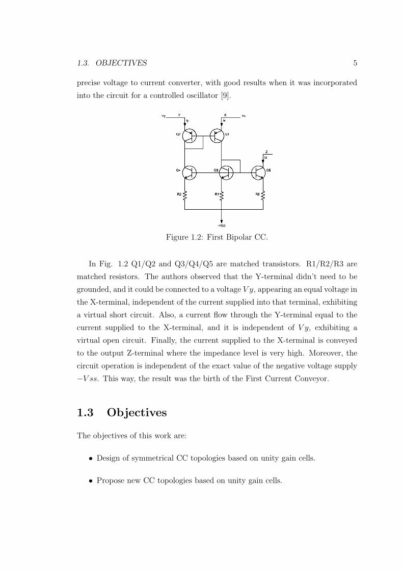
he designed the circuit shown in Fig. 1.2 where Q1 is the current source transistor,
its emitter was connected via a resistor R to a control voltage Vc. Transistor Q2 is
a compensating diode-connected transistor, its emitter was connected to ground.
Transistors Q3, Q4 and Q5 form a two-output current mirror. The mirror provided
a current to Q2 equal to that in Q1, thus making their Emitter-Base Voltage (VEB)
equal and making the voltage at the emitter of Q1 equal to zero. This in turn
made the current in Q1 equal to Vc/R. The mirror supplied an equal current
at the collector of Q5, at a high impedance level. Since Q3, Q4 and Q5 were
discrete devices, their matching was not good and emitter resistors were added
to improve the mirror performance. This circuit provided a solution to create a
1.3. OBJECTIVES 5
precise voltage to current converter, with good results when it was incorporated
into the circuit for a controlled oscillator [9].
Figure 1.2: First Bipolar CC.
In Fig. 1.2 Q1/Q2 and Q3/Q4/Q5 are matched transistors. R1/R2/R3 are
matched resistors. The authors observed that the Y-terminal didn’t need to be
grounded, and it could be connected to a voltage V y, appearing an equal voltage in
the X-terminal, independent of the current supplied into that terminal, exhibiting
a virtual short circuit. Also, a current flow through the Y-terminal equal to the
current supplied to the X-terminal, and it is independent of V y, exhibiting a
virtual open circuit. Finally, the current supplied to the X-terminal is conveyed
to the output Z-terminal where the impedance level is very high. Moreover, the
circuit operation is independent of the exact value of the negative voltage supply
−V ss. This way, the result was the birth of the First Current Conveyor.
1.3 Objectives
The objectives of this work are:
• Design of symmetrical CC topologies based on unity gain cells.
• Propose new CC topologies based on unity gain cells.
6 CHAPTER 1. INTRODUCTION
• Introduce new Nullor equivalent representations for all CC topologies pre-
sented in this work.
• Show applications for CC-based circuits (like filtering, oscillation, induc-
tance simulator applications).
1.4 Thesis Organization
The chapter distribution is as follows:
In Chapter 2 each type of CC, direct and inverted CCs as first, second and third
generation is described, each one with their variables, as positives, negatives,
multiple-output and current-controlled. All of this using unity-gain cells (UGCs)
as simple building blocks.
In Chapter 3 nullor equivalents of all CCs are introduced and they are used to
describe the analysis of CC-based circuits by applying Nodal Analysis (NA) and
symbolic analysis.
In Chapter 4 the designs of UGCs in a transistor level are described.
In Chapter 5 the designs of Direct and Inverted CCs formed by UGCs in a tran-
sistor level are described.
In Chapter 6 some applications of the CCIs, CCIIs and ICCIIs to design active
filters, oscillators and inductance simulators are shown.
In Chapter 7 the conclusions of this work are presented .
Chapter 2
Current Conveyor
The concept of the current conveyor (CC) was first presented in 1968 and further
developed to a second version or generation in 1970. The CC is considered a
general building block with practical applications. The opamp concept has been
adopted since the late of 40’s, so that it is difficult to get any other similar concept
widely accepted. However, opamps do not perform well in applications where a
current-output signal is needed, and consequently an application field for CC-
based circuits arises. It is worthy to mention that since the CC operates without
any global feedback, then it presents a different high frequency behavior compared
to opamp-based circuits [1]. In this manner, this chapter describes the three main
types or generations of CCs: First, Second and Third Generation. Each one
divided into positive-type, negative-type, direct, inverse, multiple-outputs and
current controlled.
A CC is a minimum 3-terminals device which, when is arranged with other
electronic elements in a specific circuit, can perform many useful analog signal
processing functions. The CC simplifies circuit design as the opamp does, due to
the fact that the first one offers an alternative way of abstracting complex circuit
functions. Moreover, the real behavior of a CC approaches its ideal behavior
quite closely, implying that a designer can use CCs that will work at levels that
are quite close to their predicted theoretical performance [5]. The CC can be
classified in different ways, but the principal classification is for their Generation
class. There are three types of generation, named First Generation CC or CCI,
7

8 CHAPTER 2. CURRENT CONVEYOR
Second Generation CC or CCII and Third Generation CC commonly named as
CCIII. Each type of these different generations is divided in positive or negative
CC, direct or inverted CC, Current Controlled CC, and Multiple-outputs CC. A
graphical representation of these classifications was shown in Chapter 1, in Fig.
1.1. Furthermore, in this chapter their behavior and schematic representations
are described.
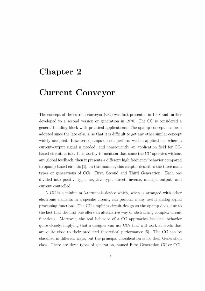
2.1 First Generation Current Conveyor (CCI)
Basically, a CCI is a three port device which can be represented by the ”black
box” shown in Fig. 2.1. As it was mentioned in Chapter 1, the first CC appeared
in 1968, invented by Sedra and K.C. Smith [6], and its behavior is described
as follows: If a voltage is applied to the input Y-terminal, an equal potential
will appear on the X-terminal. Similarly, an input current flowing through the X-
terminal will generate an equal current flowing into Y-terminal, and another equal
current will be conveyed to the output Z-terminal. The voltage in X-terminal,
established by the voltage in Y-terminal, is independent of the current forced
into X-terminal. In the same manner, the current through Y-terminal, which was
established by the current through X-terminal, is independent from the voltage
applied at the Y-terminal, due to the fact that the voltage in the X-terminal and
the current through the Y terminal are processed by a Voltage Follower and a
Current Mirror, respectively, independent between them. Thus, the CC exhibits
a virtual short-circuit input characteristic at X-terminal and a dual virtual open-
circuit input characteristic at the Y-terminal [5].
Figure 2.1: First Generation CC.
The input-output characteristics of a CCI can be described by the following
matrix equation:
2.1. FIRST GENERATION CURRENT CONVEYOR (CCI) 9
iy
vx
iz
=
0 1 0
1 0 0
0 ±1 0
vy
ix
vz
(2.1)
From Eq. (2.1) it can be determined that the current through the Y-terminal
is equal to the current flowing through the X-terminal or iy = ix, on the other
hand, the voltage in the X-terminal is equal to the voltage presented in the Y-
terminal, which is represented by vx = vy. Finally, the current flowing through
the Z-terminal is equal in value to that flowing through the X-terminal, but it can
take two directions which generates two Z-terminal current polarities, depending
if the CCI is positive or negative type (iz = ±ix).
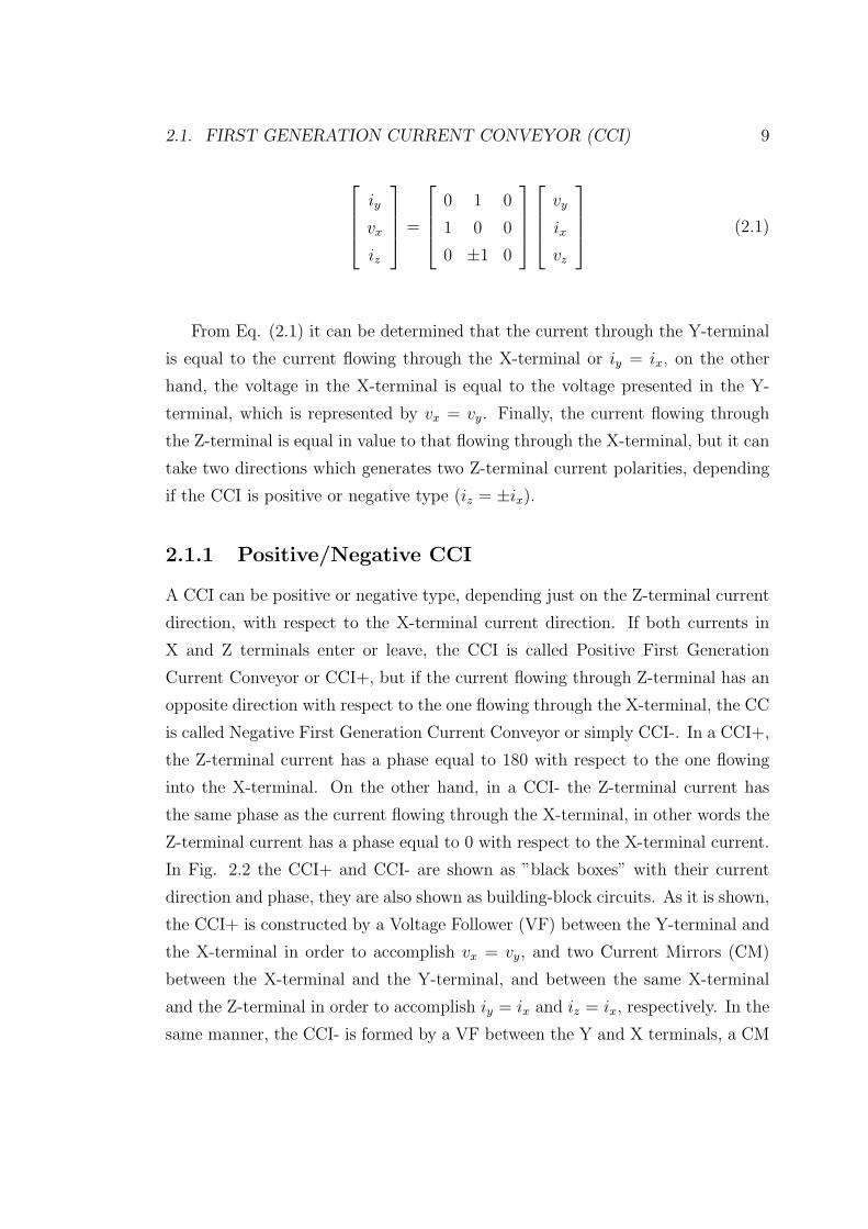
2.1.1 Positive/Negative CCI
A CCI can be positive or negative type, depending just on the Z-terminal current
direction, with respect to the X-terminal current direction. If both currents in
X and Z terminals enter or leave, the CCI is called Positive First Generation
Current Conveyor or CCI+, but if the current flowing through Z-terminal has an
opposite direction with respect to the one flowing through the X-terminal, the CC
is called Negative First Generation Current Conveyor or simply CCI-. In a CCI+,
the Z-terminal current has a phase equal to 180 with respect to the one flowing
into the X-terminal. On the other hand, in a CCI- the Z-terminal current has
the same phase as the current flowing through the X-terminal, in other words the
Z-terminal current has a phase equal to 0 with respect to the X-terminal current.
In Fig. 2.2 the CCI+ and CCI- are shown as ”black boxes” with their current
direction and phase, they are also shown as building-block circuits. As it is shown,
the CCI+ is constructed by a Voltage Follower (VF) between the Y-terminal and
the X-terminal in order to accomplish vx = vy, and two Current Mirrors (CM)
between the X-terminal and the Y-terminal, and between the same X-terminal
and the Z-terminal in order to accomplish iy = ix and iz = ix, respectively. In the
same manner, the CCI- is formed by a VF between the Y and X terminals, a CM
10 CHAPTER 2. CURRENT CONVEYOR
between the X and Y terminals and a Current Follower (CF) between the X and
Z terminals in order to accomplish iz = −ix.
Figure 2.2: Block diagram of: (a)CCI+ and (b) CCI-.
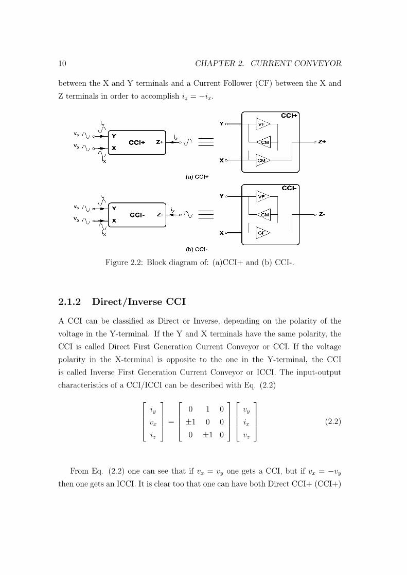
2.1.2 Direct/Inverse CCI
A CCI can be classified as Direct or Inverse, depending on the polarity of the
voltage in the Y-terminal. If the Y and X terminals have the same polarity, the
CCI is called Direct First Generation Current Conveyor or CCI. If the voltage
polarity in the X-terminal is opposite to the one in the Y-terminal, the CCI
is called Inverse First Generation Current Conveyor or ICCI. The input-output
characteristics of a CCI/ICCI can be described with Eq. (2.2)
iy
vx
iz
=
0 1 0
±1 0 0
0 ±1 0
vy
ix
vz
(2.2)
From Eq. (2.2) one can see that if vx = vy one gets a CCI, but if vx = −vy
then one gets an ICCI. It is clear too that one can have both Direct CCI+ (CCI+)
2.1. FIRST GENERATION CURRENT CONVEYOR (CCI) 11
and Inverse CCI+ (ICCI+) or both Direct CCI- (CCI-) and Inverse CCI- (ICCI-).
In Fig. 2.3 the ICCI+ and ICCI- are shown as ”black boxes” with their current
direction and phase, they are also shown as block circuits.
Figure 2.3: Block diagram of: (A) ICCI+ and (b) ICCI-
As it can be seen, the ICCI+ is constructed by a Voltage Mirror (VM) between
the Y-terminal and the X-terminal in order to accomplish vx = −vy, and two
Current Mirrors (CM) between the X-terminal and the Y-terminal, and between
the same X-terminal and the Z-terminal in order to accomplish iy = ix and iz = ix,
respectively. In the same manner, the ICCI- is formed by a VM between the Y
and X terminals, a CM between the X and Y terminals and a Current Follower
(CF) between the X and Z terminals in order to accomplish iz = −ix.
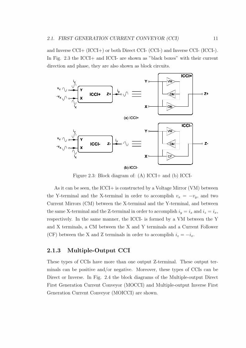
2.1.3 Multiple-Output CCI
These types of CCIs have more than one output Z-terminal. These output ter-
minals can be positive and/or negative. Moreover, these types of CCIs can be
Direct or Inverse. In Fig. 2.4 the block diagrams of the Multiple-output Direct
First Generation Current Conveyor (MOCCI) and Multiple-output Inverse First
Generation Current Conveyor (MOICCI) are shown.

12 CHAPTER 2. CURRENT CONVEYOR
Figure 2.4: Block diagram of: (a) MOCCI and (b) MOICCI.
2.1.4 Current Controlled CCI
These types of CCIs are the same as those described before, with the difference
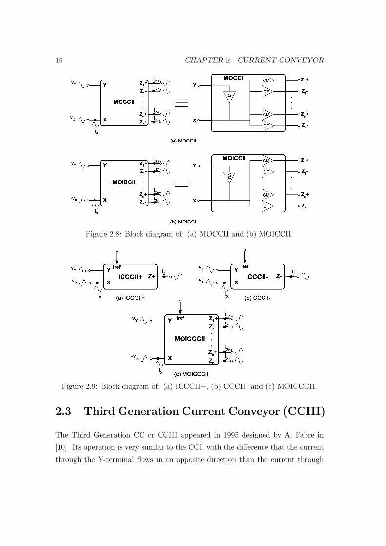
that their bias current (Iref) can be controlled externally. In Fig. 2.5 the block
diagrams of some CCIs are shown , in (a) an Inverse Current Controlled CCI+
(ICCC+) is shown, in (b) a Current Controlled CCI- (CCCI-), and finally in (c)
a Multiple-output Current Controlled ICCI (MOICCCI).
2.2 Second Generation Current Conveyor (CCII)
To increase the versatility of the CCI, a second version appeared in 1970 proposed
by the same authors Sedra and K.C. Smith [7], where no current flows in the Y-
terminal. The CCII is described by Eq. (2.3), where the Y-terminal has an
infinite input impedance. The voltage at the X-terminal follows the same one
applied to the Y-terminal, thus the X-terminal exhibits a zero input impedance.
The current supplied to the X-terminal is conveyed to the high output impedance
at the Z-terminal [5].
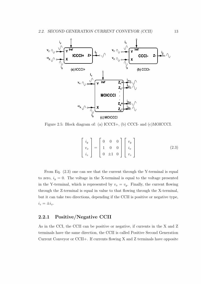
2.2. SECOND GENERATION CURRENT CONVEYOR (CCII) 13
Figure 2.5: Block diagram of: (a) ICCCI+, (b) CCCI- and (c)MOICCCI.
iy
vx
iz
=
0 0 0
1 0 0
0 ±1 0
vy
ix
vz
(2.3)
From Eq. (2.3) one can see that the current through the Y-terminal is equal
to zero, iy = 0. The voltage in the X-terminal is equal to the voltage presented
in the Y-terminal, which is represented by vx = vy. Finally, the current flowing
through the Z-terminal is equal in value to that flowing through the X-terminal,
but it can take two directions, depending if the CCII is positive or negative type,
iz = ±ix.
2.2.1 Positive/Negative CCII
As in the CCI, the CCII can be positive or negative, if currents in the X and Z
terminals have the same direction, the CCII is called Positive Second Generation
Current Conveyor or CCII+. If currents flowing X and Z terminals have opposite
14 CHAPTER 2. CURRENT CONVEYOR
directions, the CC is called Negative Second Generation Current Conveyor or
CCII-. In the same manner, this classification is just based on the currents flow
directions, but if the analysis is made in time domain, the concept is opposite to
the one described by Eq. (2.3). In Fig. 2.6 the CCII+ and CCII- are shown, where
the CCII+ is constructed by a Voltage Follower (VF) between the Y-terminal
and the X-terminal in order to accomplish vx = vy, and a Current Mirror (CM)
between the X-terminal and the Z-terminal in order to accomplish iz = ix. In the
same manner, the CCII- is formed by a VF between the Y and X terminals, and
a Current Follower (CF) between the X and Z terminals in order to accomplish
iz = −ix.
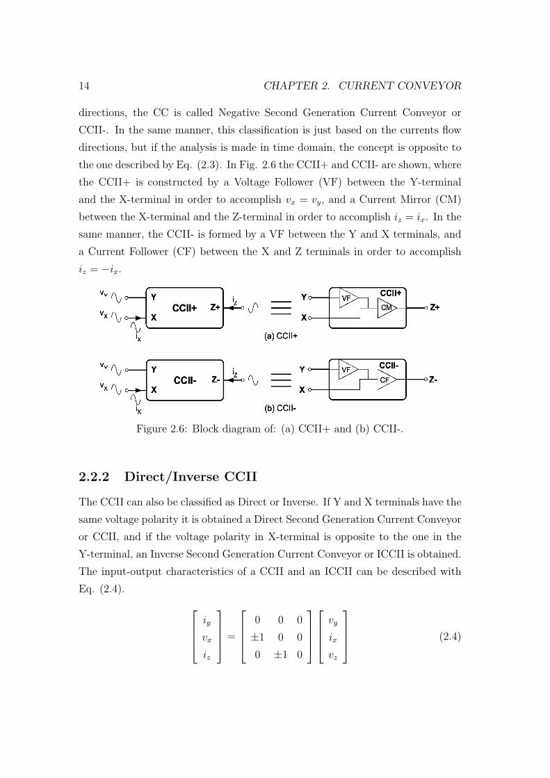
Figure 2.6: Block diagram of: (a) CCII+ and (b) CCII-.
2.2.2 Direct/Inverse CCII
The CCII can also be classified as Direct or Inverse. If Y and X terminals have the
same voltage polarity it is obtained a Direct Second Generation Current Conveyor
or CCII, and if the voltage polarity in X-terminal is opposite to the one in the
Y-terminal, an Inverse Second Generation Current Conveyor or ICCII is obtained.
The input-output characteristics of a CCII and an ICCII can be described with
Eq. (2.4).
iy
vx
iz
=
0 0 0
±1 0 0
0 ±1 0
vy
ix
vz
(2.4)

2.2. SECOND GENERATION CURRENT CONVEYOR (CCII) 15
From Eq. (2.4), when vx = vy a CCII is obtained, but when vx = −vy then an
ICCII is obtained. In Fig. 2.7 the ICCII+ and ICCII- are shown.
Figure 2.7: Block diagram of (a) ICCII+ and (b) ICCII-.
The ICCII+ is formed by a VM between the Y and X terminals in order to
accomplish vx = −vy, and a CM between the X and Z terminals in order to
accomplish iy = ix. In the same way, the ICCII- is formed by a VM between
the Y and X terminals, and a CF between the X and Z terminals in order to
accomplish iz = −ix.
2.2.3 Multiple-Output CCII
In Fig. 2.8 the block diagrams of the Multiple-output Direct Second Generation
Current Conveyor (MOCCII) and the Multiple-output Inverse Second Generation
Current Conveyor (MOICCII) are shown.
2.2.4 Current Controlled CCII
All CCIIs described before can be classified as Current Controlled ones if their
current polarization Iref is externally varied. In Fig. 2.9, they are shown in (a)
an Inverse Current Controlled CCII+ (ICCCII+), in (b) a Current Controlled
CCII- (CCCII-) and in (c) a Multiple-output Inverse Current Controlled CCII
(MOICCCII).
16 CHAPTER 2. CURRENT CONVEYOR
Figure 2.8: Block diagram of: (a) MOCCII and (b) MOICCII.
Figure 2.9: Block diagram of: (a) ICCCII+, (b) CCCII- and (c) MOICCCII.
2.3 Third Generation Current Conveyor (CCIII)
The Third Generation CC or CCIII appeared in 1995 designed by A. Fabre in
[10]. Its operation is very similar to the CCI, with the difference that the current
through the Y-terminal flows in an opposite direction than the current through

2.3. THIRD GENERATION CURRENT CONVEYOR (CCIII) 17
the X-terminal. The input-output characteristics of the CCIII are described by
Eq. (2.5).
iy
vx
iz
=
0 −1 0
1 0 0
0 ±1 0
vy
ix
vz
(2.5)
From Eq. (2.5) one can see that the current through the Y-terminal is equal
to the current through the X-terminal but with an opposite direction (iy = −ix).
The voltage in the X-terminal is equal to the voltage in the Y-terminal, which
is represented by vx = vy. Finally the current through the Z-terminal is equal
in value to that flowing through the X-terminal, but it can take two directions,
depending if the CCIII is positive or negative type, iz = ±ix.
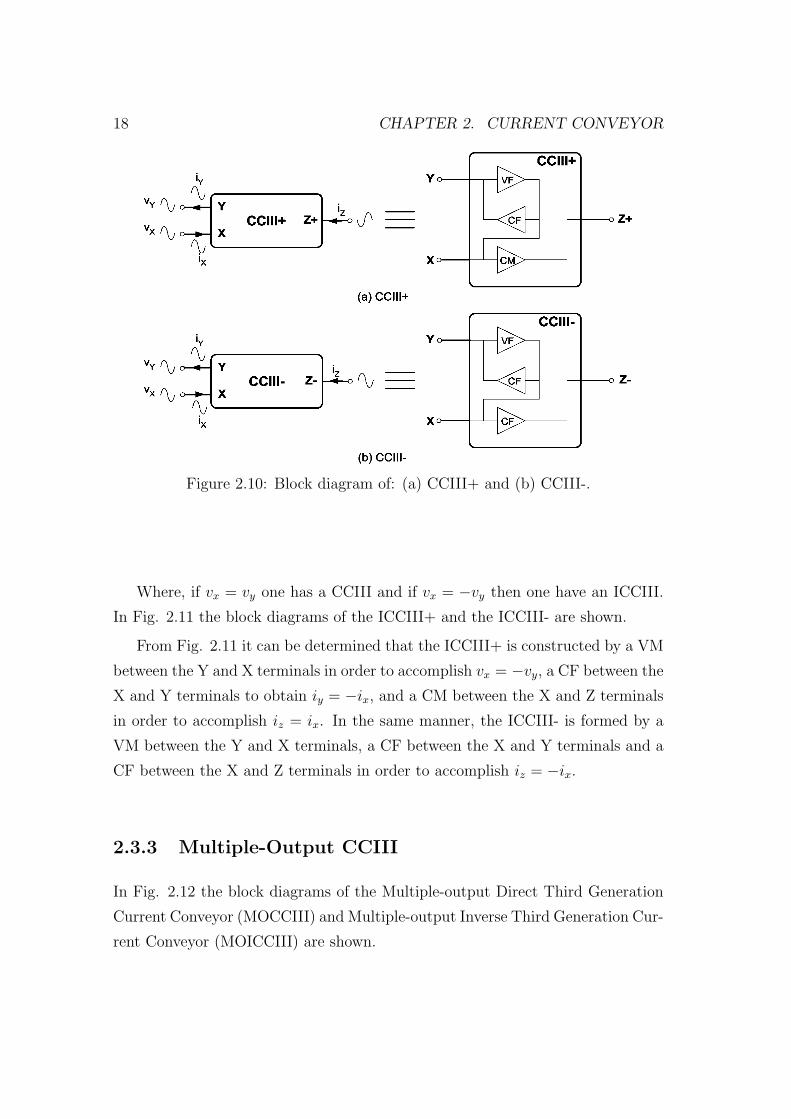
2.3.1 Positive/Negative CCIII
In the same manner as the CCI and CCII, the CCIII can be positive or negative.
In Fig. 2.10 the CCIII+ and CCIII- block diagrams are shown. The CCIII+ is
formed by a Voltage Follower (VF) between the Y-terminal and the X-terminal in
order to accomplish vx = vy, and a Current Mirror (CM) between the X-terminal
and the Y-terminal in order to accomplish iz = ix. In the same manner, the
CCIII- is formed by a VF between the Y and X terminals, and a Current Follower
(CF) between the X and Z terminals in order to accomplish iz = −ix.
2.3.2 Direct/Inverse CCIII
The input-output characteristics of the CCIII and ICCIII are described by Eq.
(2.6).
iy
vx
iz
=
0 −1 0
±1 0 0
0 ±1 0
vy
ix
vz
(2.6)
18 CHAPTER 2. CURRENT CONVEYOR
Figure 2.10: Block diagram of: (a) CCIII+ and (b) CCIII-.
Where, if vx = vy one has a CCIII and if vx = −vy then one have an ICCIII.
In Fig. 2.11 the block diagrams of the ICCIII+ and the ICCIII- are shown.
From Fig. 2.11 it can be determined that the ICCIII+ is constructed by a VM
between the Y and X terminals in order to accomplish vx = −vy, a CF between the
X and Y terminals to obtain iy = −ix, and a CM between the X and Z terminals
in order to accomplish iz = ix. In the same manner, the ICCIII- is formed by a
VM between the Y and X terminals, a CF between the X and Y terminals and a
CF between the X and Z terminals in order to accomplish iz = −ix.
2.3.3 Multiple-Output CCIII
In Fig. 2.12 the block diagrams of the Multiple-output Direct Third Generation
Current Conveyor (MOCCIII) and Multiple-output Inverse Third Generation Cur-
rent Conveyor (MOICCIII) are shown.

2.3. THIRD GENERATION CURRENT CONVEYOR (CCIII) 19
Figure 2.11: Block diagram of (a) ICCIII+ and (b) ICCIII-.
Figure 2.12: Block diagram of: (a) MOCCIII and (b) MOICCIII.
2.3.4 Current Controlled CCIII
In Fig. 2.13 it is shown in (a) an Inverse Current Controlled CCIII+ (ICCCIII+),
in (b) a Current Controlled CCIII- (CCCIII-) and in (c) a MO Inverse Current

20 CHAPTER 2. CURRENT CONVEYOR
Controlled CCIII (MOICCCIII).
Figure 2.13: Block diagram of: (a) ICCCIII, (b) CCCIII- and (c)MOICCCIII.
Chapter 3
Nullor
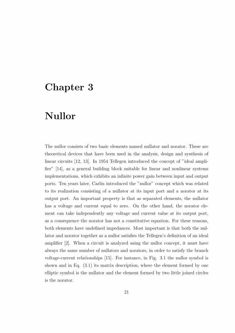
The nullor consists of two basic elements named nullator and norator. These are
theoretical devices that have been used in the analysis, design and synthesis of
linear circuits [12, 13]. In 1954 Tellegen introduced the concept of ”ideal ampli-
fier” [14], as a general building block suitable for linear and nonlinear systems
implementations, which exhibits an infinite power gain between input and output
ports. Ten years later, Carlin introduced the ”nullor” concept which was related
to its realization consisting of a nullator at its input port and a norator at its
output port. An important property is that as separated elements, the nullator
has a voltage and current equal to zero. On the other hand, the norator ele-
ment can take independently any voltage and current value at its output port,
as a consequence the norator has not a constitutive equation. For these reasons,
both elements have undefined impedances. Most important is that both the nul-
lator and norator together as a nullor satisfies the Tellegen’s definition of an ideal
amplifier [2]. When a circuit is analyzed using the nullor concept, it must have
always the same number of nullators and norators, in order to satisfy the branch
voltage-current relationships [15]. For instance, in Fig. 3.1 the nullor symbol is
shown and in Eq. (3.1) its matrix description, where the element formed by one
elliptic symbol is the nullator and the element formed by two little joined circles
is the norator.
21

22 CHAPTER 3. NULLOR
Figure 3.1: Nullor symbol.
[V1
I1
]=
[0 0
0 0
] [V2
I2
](3.1)
3.1 Nullor Equivalents
The nullor element is a very ideal useful device for circuit analysis. This element
can be connected in different ways to generate the model of an active device or
circuit, in order to simplify the analysis process. Some basic nullor-equivalents
are shown in Fig. 3.2, which can be applied in circuit analysis.
Figure 3.2: Basic nullor equivalents.
From Fig. 3.2 is clear in the case (a) that through the series connection of a
nullator and a norator (from A to B) cannot flow any current because the nullator
current is zero, so in this case an Open Circuit equivalent is obtained. In the case
3.1. NULLOR EQUIVALENTS 23
(b) a current flows from A to B through the norator and the voltage between A
and B is zero from the property of the nullator, so the result is a Short Circuit
equivalent. In the case (c) no current flows from A to B because of the properties
of the nullator where voltage across its terminals is zero, then a nullator with these
two elements is equal to a single nullator. In the case (d) a current flows from A
to B, but the voltage is not defined between the norator terminals, so that the
circuit equivalent is equal to a single norator. In the case (e) the voltage difference
between A and B is zero and no current flows through these terminals because
of the nullator properties; the voltage between A-C and B-D is not defined and
no current flows from C-D through the norator to A or B because there are two
nullators blocking it. In the case (f) a current flows from A to B but no current
flows through the nullator. Finally in the case (g) the voltage between A and C
is zero, but no current flows between these two terminals. On the other hand, the
voltage is undefined between B and D, but there is a current that flows through
these terminals, so that the equivalent is the same as an ideal amplifier. By using
the basic nullor equivalents, a nullor can be used to generate electrical equivalents
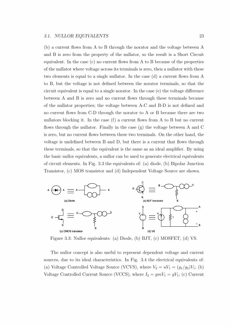
of circuit elements. In Fig. 3.3 the equivalents of: (a) diode, (b) Bipolar Junction
Transistor, (c) MOS transistor and (d) Independent Voltage Source are shown.
Figure 3.3: Nullor equivalents: (a) Diode, (b) BJT, (c) MOSFET, (d) VS.
The nullor concept is also useful to represent dependent voltage and current
sources, due to its ideal characteristics. In Fig. 3.4 the electrical equivalents of:
(a) Voltage Controlled Voltage Source (VCVS), where V2 = uV1 = (g1/g2)V1; (b)
Voltage Controlled Current Source (VCCS), where I2 = gmV1 = gV1; (c) Current

24 CHAPTER 3. NULLOR
Controlled Voltage Source (CCVS), where V2 = rI1 = I1/g; and (d) Current
Controlled Current Source (CCCS), where I2 = BI1 = (g2/g1)I1 are shown.
Figure 3.4: Nullor equivalents: (a) VCVS, (b) VCCS, (c) CCVS, (d) CCCS.
It is possible to represent ideal amplifiers with nullor equivalents [11]. For
example, in Fig. 3.5 the equivalents of: (a) Opamp, where V out = Av(V+ − V−);
(b) OTA (Operational Transconductance Amplifier), where Iout = gm(V+− V−);
(c) OTRA (Operational Transresistance Amplifier), where V out = (I+− I−)/gm;
and (d) COA (Current Operational Amplifier), where Iout = Ai(I+ − I−) are
shown. In [15] are more nullor equivalents and their equations.
3.2 Current Conveyor Nullor Equivalents
As one can infer, the nullor concept is quite useful to generate ideal equivalents of
circuit elements. As a consequence one can generate the ideal equivalent of each
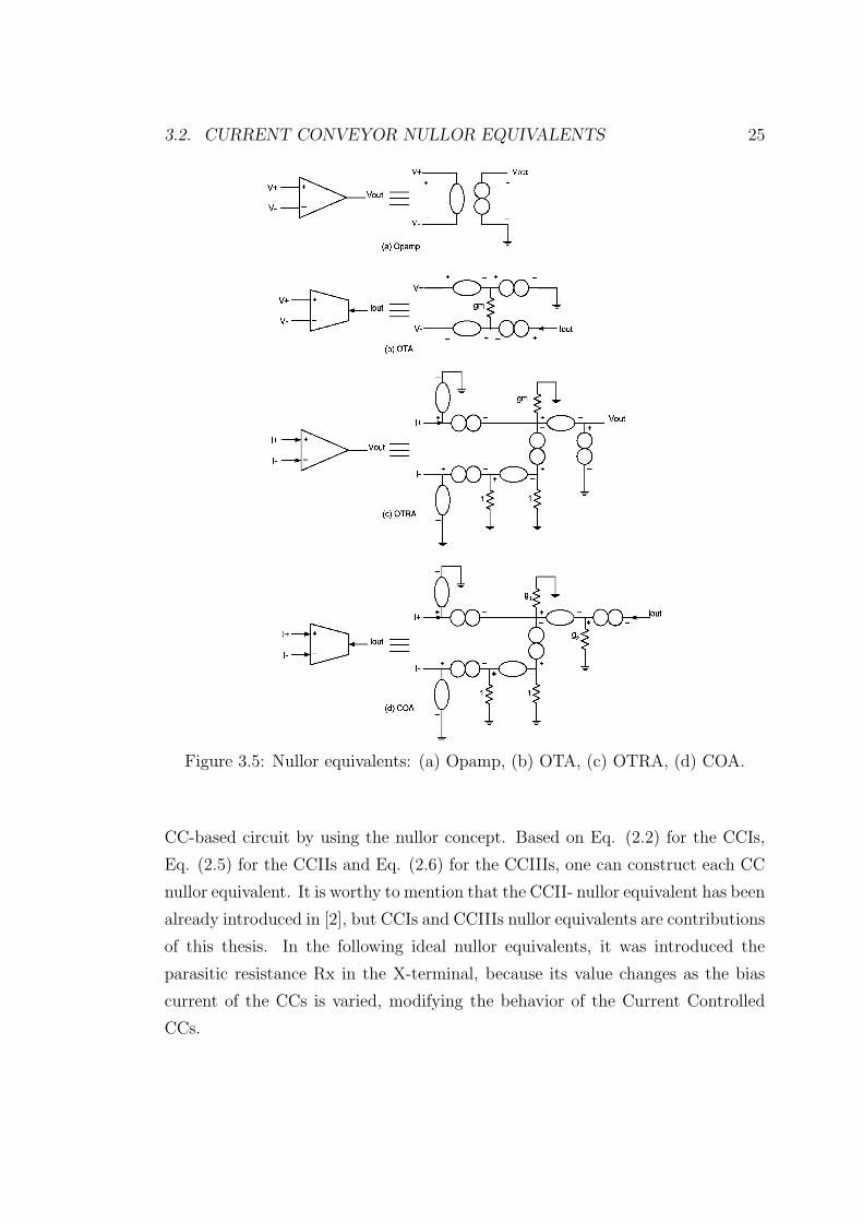
3.2. CURRENT CONVEYOR NULLOR EQUIVALENTS 25
Figure 3.5: Nullor equivalents: (a) Opamp, (b) OTA, (c) OTRA, (d) COA.
CC-based circuit by using the nullor concept. Based on Eq. (2.2) for the CCIs,
Eq. (2.5) for the CCIIs and Eq. (2.6) for the CCIIIs, one can construct each CC
nullor equivalent. It is worthy to mention that the CCII- nullor equivalent has been
already introduced in [2], but CCIs and CCIIIs nullor equivalents are contributions
of this thesis. In the following ideal nullor equivalents, it was introduced the
parasitic resistance Rx in the X-terminal, because its value changes as the bias
current of the CCs is varied, modifying the behavior of the Current Controlled
CCs.
26 CHAPTER 3. NULLOR
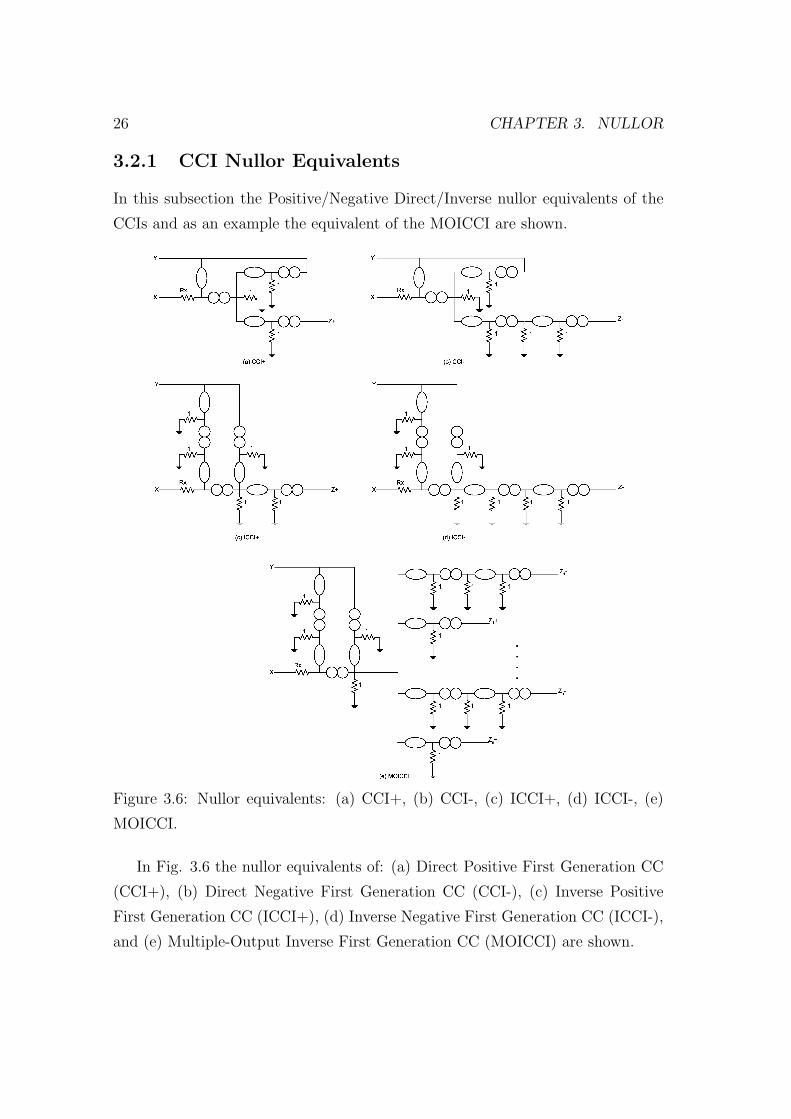
3.2.1 CCI Nullor Equivalents
In this subsection the Positive/Negative Direct/Inverse nullor equivalents of the
CCIs and as an example the equivalent of the MOICCI are shown.
Figure 3.6: Nullor equivalents: (a) CCI+, (b) CCI-, (c) ICCI+, (d) ICCI-, (e)
MOICCI.
In Fig. 3.6 the nullor equivalents of: (a) Direct Positive First Generation CC
(CCI+), (b) Direct Negative First Generation CC (CCI-), (c) Inverse Positive
First Generation CC (ICCI+), (d) Inverse Negative First Generation CC (ICCI-),
and (e) Multiple-Output Inverse First Generation CC (MOICCI) are shown.
3.2. CURRENT CONVEYOR NULLOR EQUIVALENTS 27
3.2.2 CCII Nullor Equivalents
In this subsection the Positive/Negative Direct/Inverse nullor equivalents of the
CCIIs, and as an example the equivalent of the MOCCII are shown. In Fig. 3.7
the nullor equivalents of: (a) Direct Positive Second Generation CC (CCII+),
(b) Direct Negative Second Generation CC (CCII-), (c) Inverse Positive Second
Generation CC (ICCII+), (d) Inverse Negative Second Generation CC (ICCII-),
and (e) Multiple-Output Direct Second Generation CC (MOCCII) are shown.
3.2.3 CCIII Nullor Equivalents
The CCIII is not a very popular topology in the literature currently found. It has
been introduced in [10], and in this subsection the CCIIIs nullor equivalents are
shown.
In Fig. 3.8 the nullor equivalents of: (a) Direct Positive Third Generation
CC (CCIII+), (b) Direct Negative Third Generation CC (CCIII-), (c) Inverse
Positive Third Generation CC (ICCIII+), (d) Inverse Negative Third Generation
CC (ICCIII-), and (e) Multiple-Output Inverse Third Generation CC (MOICCIII)
are shown.

28 CHAPTER 3. NULLOR
Figure 3.7: Nullor equivalents: (a) CCII+, (b) CCII-, (c) ICCII+, (d) ICCII-, (e)
MOCCII.

3.2. CURRENT CONVEYOR NULLOR EQUIVALENTS 29
Figure 3.8: Nullor equivalents: (a) CCIII+, (b) CCIII-, (c) ICCIII+, (d) ICCII-,
(e) MOICCIII.

30 CHAPTER 3. NULLOR
3.3 Analysis of CC-Based Circuits
In the way to use the Nullor equivalents in circuit analysis, this subsection de-
scribes the Nodal Analysis (NA) applied to CC-based circuits. Although in [15]
one can find all CCIIs nullor equivalents, in this work the CCIs and CCIIIs nullor
equivalents are introduced.
3.3.1 Nodal Analysis (NA)
By applying symbolic techniques the NA is based on the idea of generating the
fully symbolic circuit equations directly from the circuit description, and then
putting them into the following general matrix form:
Ax = b (3.2)
where A is a symbolic matrix of dimension n × n, x is a vector of circuit
variables of length n, and b is a symbolic vector of constants of length n; n is the
number of circuit variables: Currents, voltages, charges or fluxes. The analysis
proceeds by solving Eq. (3.2) for x [15]. The first step in NA is to formulate
the linear admittance matrix Y. The circuit variables are the voltage nodes which
are included in the variable vector v, and vector i represents the values of all
independent Current sources of the circuit. The ith entry in i represents a current
source entering in the ith node. There will be nV voltage nodes, v and i dimensions
will be of nv × 1. After this, the nodal linear system of equations is represented
in the following matrix form:
Y v = i (3.3)
Row i of Y represents the Kirchhoff’s Current Law (KCL) equation at node
i. Y is constructed by writing KCL equations at each node, except for the datum
node. The ith equation then would state that sum of all currents leaving node i
and is equal to zero. The equations are then set into the matrix form of Eq. (3.3).
Building the linear admittance matrix of CC-based circuits, it is convenient to
use the nullor equivalents to model the behavior of all CCs, and the NA is then
performed as shown in the following section.
3.3. ANALYSIS OF CC-BASED CIRCUITS 31
3.3.2 NA of CC-Based circuits using nullors.
Based in the NA described in [15, 16, 17], in this section some circuits consisting
of CCI+s, ICC+s and ICCIII-s are analyzed, in order to verify the usefulness of
the nullor equivalents. The NA can be summarized in the following steps:
Step 1: Obtaining the nullor circuit equivalent and label each node.
Step 2: Building the linear admittance matrix as it is done in [16].
Step 3: Reducing the admittance matrix:
a) Adding the columns that correspond to those nodes sharing a nullator
element.
b) Adding the rows that correspond to those nodes sharing a norator ele-
ment.
c) Eliminating those columns that correspond to a node connected to a
grounded nullator.
d)Eliminating those rows that correspond to a node connected to a grounded
norator.
Step 4: Solve the matrix system for v in Eq. (3.3).
CCI+ analysis:
Taking the circuit in Fig. 3.9(a), the nullor equivalent of the CCI+ is shown in
Fig. 3.6, and the nullor equivalent of the independent voltage source is shown in
Fig. 3.3, so that the nullor equivalent of Fig. 3.9(a) is shown in Fig. 3.9(b), where
each node has a name inside a circle (Step 1).
By applying the NA method given in [16] to Fig. 3.9(b), one obtains the
system given in Eq. (3.4) (Step 2):

32 CHAPTER 3. NULLOR
Figure 3.9: (a) CCI+ and (b) Nullor equivalent of (a).
0
0
0
0
VIN
0
0
0
=
1 0 0 0 0 0 0 0
0 gx 0 0 0 0 −gx 0
0 0 1 0 0 0 0 0
0 0 0 1 0 0 0 0
0 0 0 0 1 0 0 0
0 0 0 0 0 0 0 0
0 −gx 0 0 0 0 gx + g1 0
0 0 0 0 0 0 0 gZ
V1
V2
V3
V4
V5
VY
VX
VZ
(3.4)
Reducing the matrix of Eq. (3.4) as Step 3 says:
a)Adding columns corresponding to nodes: 1-3-4, 2-Y-5:
0
0
0
0
VIN
0
0
0
=
1 0 0 0
0 gx −gx 0
1 0 0 0
1 0 0 0
0 1 0 0
0 −gx gx + g1 0
0 0 0 gZ
V1,3,4
V2,Y,5
VX
VZ
(3.5)
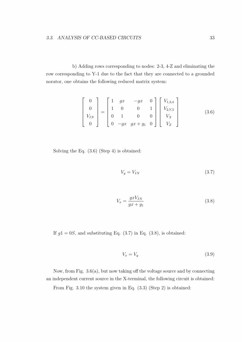
3.3. ANALYSIS OF CC-BASED CIRCUITS 33
b) Adding rows corresponding to nodes: 2-3, 4-Z and eliminating the
row corresponding to Y-1 due to the fact that they are connected to a grounded
norator, one obtains the following reduced matrix system:
0
0
VIN
0
=
1 gx −gx 0
1 0 0 1
0 1 0 0
0 −gx gx + g1 0
V1,3,4
V2,Y,5
VX
VZ
(3.6)
Solving the Eq. (3.6) (Step 4) is obtained:
Vy = VIN (3.7)
Vx =gxVIN
gx + g1
(3.8)
If g1 = 0S, and substituting Eq. (3.7) in Eq. (3.8), is obtained:
Vx = Vy (3.9)
Now, from Fig. 3.6(a), but now taking off the voltage source and by connecting
an independent current source in the X-terminal, the following circuit is obtained:
From Fig. 3.10 the system given in Eq. (3.3) (Step 2) is obtained:
34 CHAPTER 3. NULLOR
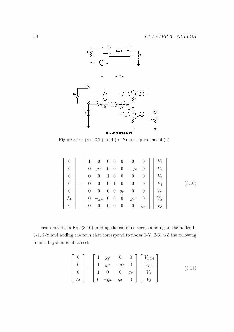
Figure 3.10: (a) CCI+ and (b) Nullor equivalent of (a).
0
0
0
0
0
Ix
0
=
1 0 0 0 0 0 0
0 gx 0 0 0 −gx 0
0 0 1 0 0 0 0
0 0 0 1 0 0 0
0 0 0 0 gY 0 0
0 −gx 0 0 0 gx 0
0 0 0 0 0 0 gZ
V1
V2
V3
V4
VY
VX
VZ
(3.10)
From matrix in Eq. (3.10), adding the columns corresponding to the nodes 1-
3-4, 2-Y and adding the rows that correspond to nodes 1-Y, 2-3, 4-Z the following
reduced system is obtained:
0
0
0
Ix
=
1 gY 0 0
1 gx −gx 0
1 0 0 gZ
0 −gx gx 0
V1,3,4
V2,Y
VX
VZ
(3.11)
3.3. ANALYSIS OF CC-BASED CIRCUITS 35
Solving Eq. (3.11):
Vy = −Ix
gY
(3.12)
Vz = −Ix
gZ
(3.13)
The minus sign indicates that currents are in the opposite direction, so by
reordering Eqs. (3.12) and (3.13) one obtains:
Iy = Ix (3.14)
Iz = Ix (3.15)
So, Eqs. (3.9), (3.14) and (3.15) describe the behavior of a CCI+, which was
described in Chapter 2 by Eq. (2.2).
ICCI+ analysis:
As a second example, lets consider the nullor-based ICCI+ equivalent shown in
Fig. 3.6(c), and connecting to the Y-terminal the independent voltage source
nullor equivalent shown in Fig. 3.3(d) to follow Step 1, then it results in the
circuit equivalent shown in Fig. 3.11(b).
0
0
0
VIN
0
=
1 1 0 0 0
0 gx 1 −gx 0
0 0 1 0 gZ
1 0 0 0 0
0 −gx 0 gx + g1 0
V1,Y,7
V2,4
V3,5,6
VX
VZ
(3.16)
Solving the system:

36 CHAPTER 3. NULLOR
Figure 3.11: (a) ICCI+ and (b) Nullor equivalent of (a).
Vy = VIN (3.17)
Vx = − gxVIN
gx + g1
(3.18)
If g1 = 0S and substituting Eq. (3.17) in Eq. (3.18) is obtained:
Vx = −Vy (3.19)
In order to obtain the other equations that describe the behavior of the ICCI+,
take off the independent voltage source from the Y-terminal and connect an in-
dependent current source at the X-terminal to obtain the circuit shown in Fig.
3.12, whose reduced system is:
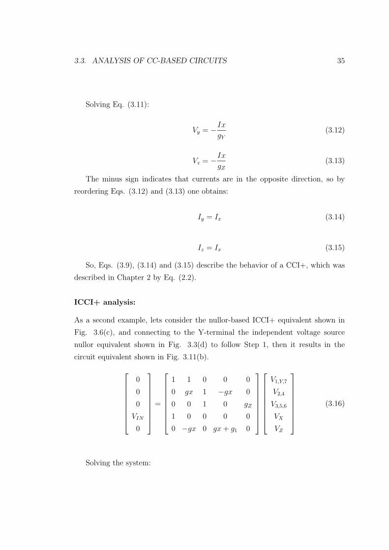
3.3. ANALYSIS OF CC-BASED CIRCUITS 37
0
0
0
0
Ix
=
1 1 0 0 0
gY 0 1 0 0
0 gx 1 −gx 0
0 0 1 0 gZ
0 −gx 0 gx 0
V1,Y
V2,4
V3,5,6
VX
VZ
(3.20)
Solving the system in Eq. (3.20) is obtained:
Vy = −Ix
gy
(3.21)
Vz = −Ix
gz
(3.22)
Figure 3.12: (a) ICCI+ and (b) Nullor equivalent of (a).
Again, the minus sign indicates that currents are in the opposite direction, so
by reordering Eqs. (3.21) and (3.22) is obtained:
38 CHAPTER 3. NULLOR
Iy = Ix (3.23)
Iz = Ix (3.24)
Therefore, Eqs. (3.19), (3.23) and (3.24) describe the behavior of an ICCI+,
which was described in Chapter 2 by Eq. (2.2).
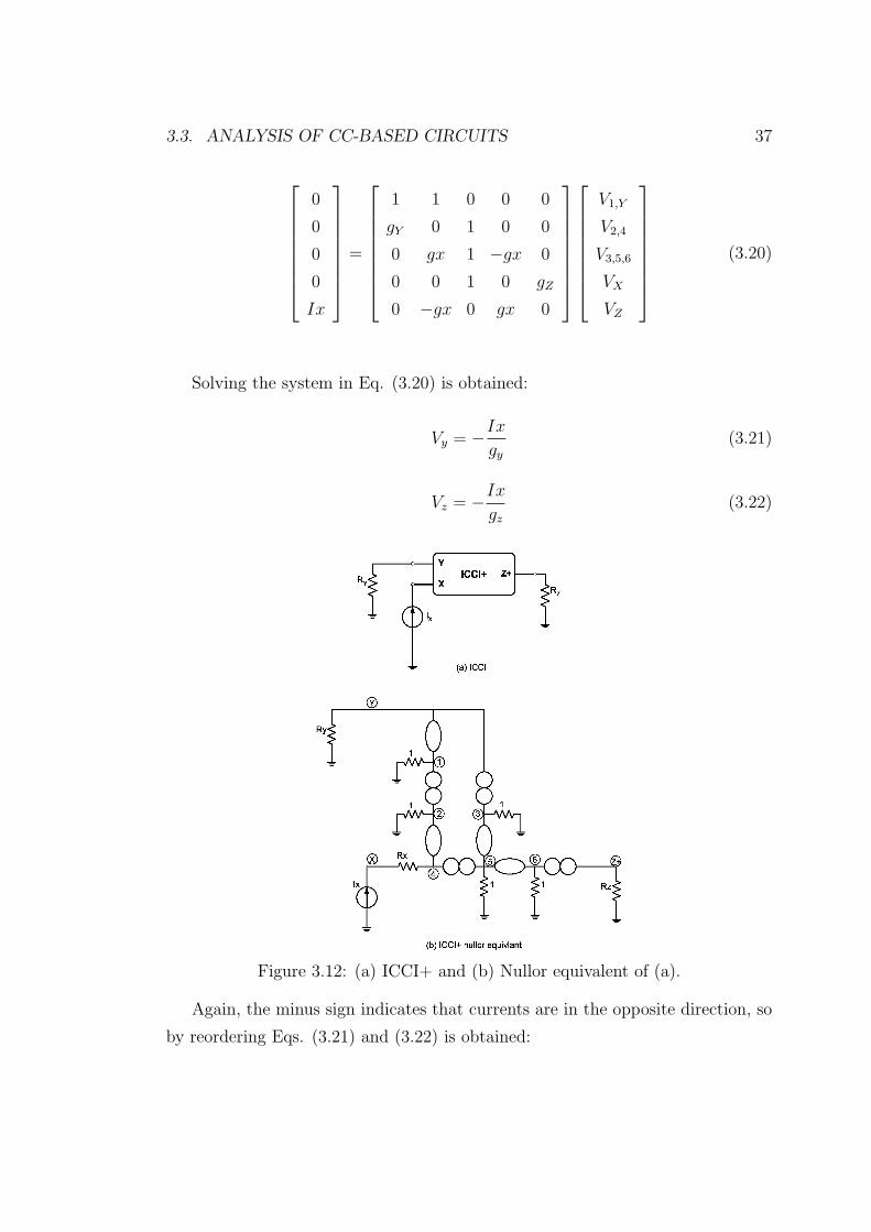
ICCIII- analysis
Following the procedure of the previous sections, let us connect an independent
voltage source in the Y-terminal of an ICCIII- in order to obtain the voltage
behavior:
Figure 3.13: (a) ICCIII- and (b) Nullor equivalent of (a).
The reduced matrix obtained from Fig. 3.13 is:
3.3. ANALYSIS OF CC-BASED CIRCUITS 39
0
0
0
0
0
Iin
0
=
1 1 0 0 0 0 0
0 0 1 1 0 0 0
0 gx 0 1 0 −gx 0
0 0 0 1 1 0 0
0 0 0 0 1 0 gZ
1 0 0 0 0 0 0
0 −gx 0 0 0 gx 0
V1,Y,11
V2,6
V3,4
V5,7,8
V9,10
VX
VZ
(3.25)
Solving the system in Eq. (3.25):
Vy = VIN (3.26)
Vx = − gxVIN
gx + g1
(3.27)
If g1 = 0S and by substituting Eq. (3.26) in Eq. (3.27):
Vx = −Vy (3.28)
Afterwards, in order to obtain the equations that describe the current behavior
of the ICCIII-, taking off the independent voltage source at the Y-terminal and
connecting an independent current source to the X-terminal, the following circuit
is obtained:
The matrix system obtained from Fig. 3.14 is:
0
0
0
0
0
0
Ix
=
1 1 0 0 0 0 0
gY 0 1 0 0 0 0
0 0 1 1 0 0 0
0 gx 0 1 0 −gx 0
0 0 0 1 1 0 0
0 0 0 0 1 0 gZ
0 −gx 0 0 0 gx 0
V1,Y
V2,6
V3,4
V5,7,8
V9,10
VX
VZ
(3.29)
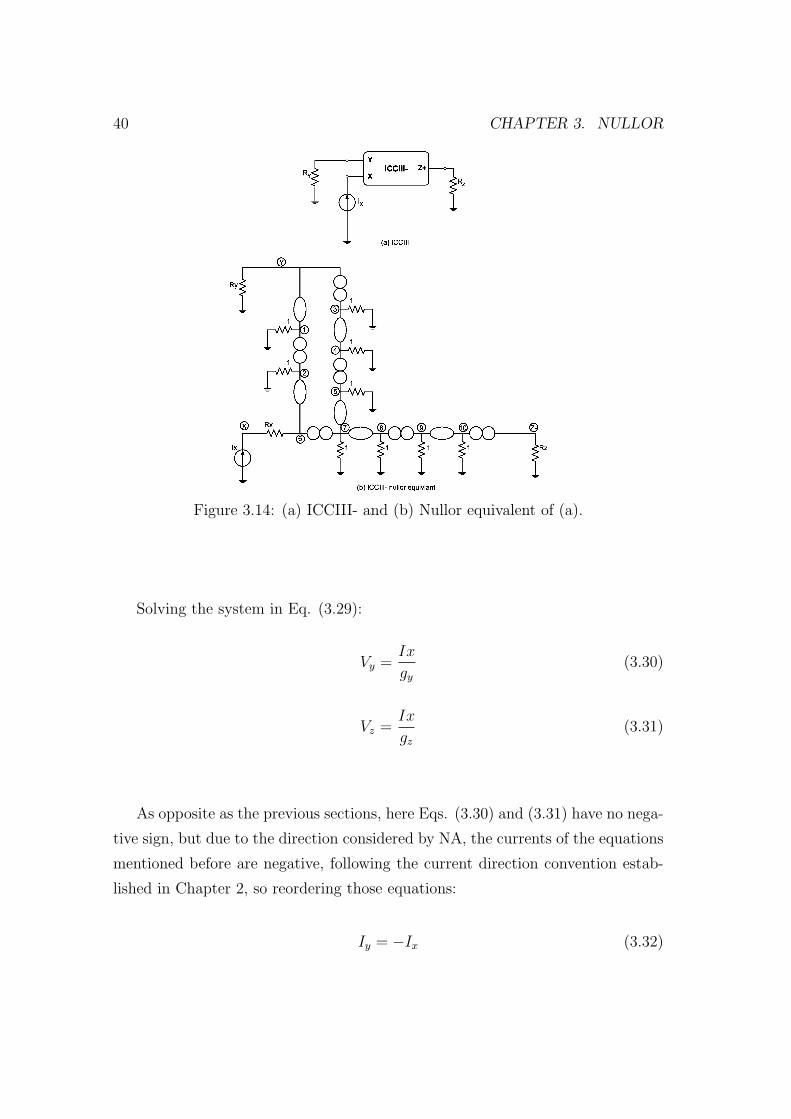
40 CHAPTER 3. NULLOR
Figure 3.14: (a) ICCIII- and (b) Nullor equivalent of (a).
Solving the system in Eq. (3.29):
Vy =Ix
gy
(3.30)
Vz =Ix
gz
(3.31)
As opposite as the previous sections, here Eqs. (3.30) and (3.31) have no nega-
tive sign, but due to the direction considered by NA, the currents of the equations
mentioned before are negative, following the current direction convention estab-
lished in Chapter 2, so reordering those equations:
Iy = −Ix (3.32)

3.4. NULLOR-BASED CURRENT MODE UNIVERSAL FILTER 41
Iz = −Ix (3.33)
Therefore, Eqs. (3.28), (3.32) and (3.33) describe the behavior of an ICCIII-
which was described also in Chapter 2 by Eq. (2.6).
3.4 Nullor-Based Current Mode Universal Fil-
ter
In this section the analysis of a Dual-Output CCII-based current-mode universal
filter taken from [18] is shown, using the CC nullor equivalent. The filter topology
is shown in Fig. 3.15 and its nullor equivalent in Fig. 3.16. The reduced matrix
system is given by Eq. (3.34) and the transfer function is given by Eq. (3.35),
where Iout was obtained by evaluating Iout = gLV0 . From Eq. (3.35), the transfer
function of each filter is obtained by setting: I1 = Iin and I2 = I3 = 0 for
low-pass (LP) response, I2 = Iin and I1 = I3 = 0, for band-pass, −I1 = I2 =
I3 = Iin for high-pass, and I2 = I3 = Iin and I1 = 0, for Notch response.
Figure 3.15: Current-mode DOCCII-based universal filter topology.
42 CHAPTER 3. NULLOR
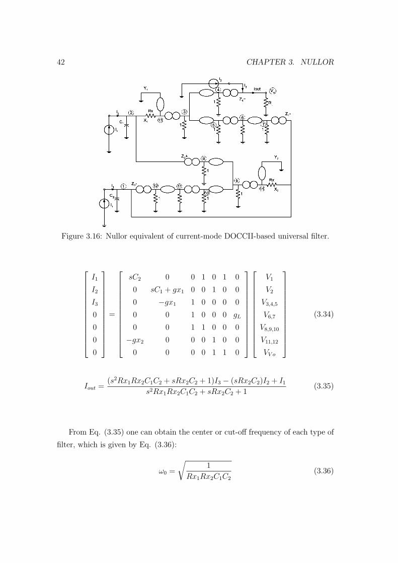
Figure 3.16: Nullor equivalent of current-mode DOCCII-based universal filter.
I1
I2
I3
0
0
0
0
=
sC2 0 0 1 0 1 0
0 sC1 + gx1 0 0 1 0 0
0 −gx1 1 0 0 0 0
0 0 1 0 0 0 gL
0 0 1 1 0 0 0
−gx2 0 0 0 1 0 0
0 0 0 0 1 1 0
V1
V2
V3,4,5
V6,7
V8,9,10
V11,12
VV o
(3.34)
Iout =(s2Rx1Rx2C1C2 + sRx2C2 + 1)I3 − (sRx2C2)I2 + I1
s2Rx1Rx2C1C2 + sRx2C2 + 1(3.35)
From Eq. (3.35) one can obtain the center or cut-off frequency of each type of
filter, which is given by Eq. (3.36):
ω0 =
√1
Rx1Rx2C1C2
(3.36)

3.4. NULLOR-BASED CURRENT MODE UNIVERSAL FILTER 43
For a frequency response of 3 MHz, the following values result: C1 = C2 =
15pF and Rx1 = Rx2 = 3.5KΩ. The responses of the filter are derived by setting:
I1 = Iin and I2 = I3 = 0 for low-pass (LP) response, I2 = Iin and I1 = I3 = 0,
for band-pass (BP), −I1 = I2 = I3 = Iin for high-pass (HP), and I2 = I3 = Iin
and I1 = 0, for Notch response. The ideal responses are shown in Fig. 3.17. The
LP response appears with a dashed line, BP with a dashed-dot line, HP with a
dotted line and the Notch response is in a solid line.
Figure 3.17: Ideal responses of the current-mode universal filter.

44 CHAPTER 3. NULLOR
Chapter 4
Unity Gain Cells (UGCs)
As it was shown in Chapter 2, the CCs can be designed by superimposing or
making cascade connections of Unity Gain Cells (UGC): Voltage Follower (VF),
Current Follower (CF), Voltage Mirror (VM) or Current Mirror (CM) [22]. In
this section these four UGCs are designed at a transistor level, in order to build
each CC.
4.1 Voltage Follower (VF)
The VFs are one of the most indispensable blocks in analog circuits. The ideal
VF presents infinite input and zero output impedance, a gain equal to unity and
no distortion of the input signal [23, 24]. Its implementation using conventional
opamps with unity gain feedback has severe limitations in the input and output
voltage swings due to the voltage required for the tail current in the front-end
differential amplifier and voltage required for the common drain type at the output
stage, respectively [25]. In this work three VFs will be used in order to construct
the CCs. These three transistor-based VFs structures are shown in Fig. 4.1.
In order to measure their electrical parameters, the ideal current sources were
substituted by simple current mirrors. The VFs presented in this work are class-
AB type, which are characterized by a low quiescent power consumption and a
high driving capability, taking current from the supply sources only when the load
requires it. Therefore class-AB circuits are considered to be good candidates for
45

46 CHAPTER 4. UNITY GAIN CELLS (UGCS)
Figure 4.1: Voltage Followers: (a) VF-A, (b) VF-B and (c) VF-C.
low-power analog design [26].
4.1.1 VF-A
This class-AB VF is the most used VF structure in CCs design. It has been
reported in [22, 25, 26, 27, 34]. Its implementation with transistor-level bias
circuit is shown in Fig. 4.2:
This VF provides good control and high effectiveness in the use of the quiescent
current. The circuit has relatively low voltage offset which is determined mainly
by transistor mismatch [25].
From Fig. 4.2, M1, M2, M3 and M4 are the core of the VF, while M5-M10 and
Mx work as CMs with the only purpose to bias the VF core. The current through
M3 and M4 has the same value as the current through M1 and M2, because M5
and M6 are mirroring the Iref current to the branches formed by M7/M8 and
M9/M10. When an AC signal is injected to V in node, it varies the M1 and M2
gate-source voltage (VGS1 and VGS2), which produces a variation in the current
circulating through these transistors. This current variation is mirrored to the
branch formed by M3 and M4, obtaining a voltage variation at Vout node, which
is directly proportional to the variation in the Vin node. Because aspect ratios
between all NMOS and between all PMOS are equal, the voltage gain in the Vout
4.1. VOLTAGE FOLLOWER (VF) 47
Figure 4.2: VF-A.
node respect to the Vin node is ideally unity. In order to calculate each transistor
aspect ratio in the VF-A, one assigns the node voltages in the circuit, which are
shown in Fig. 4.3:
Figure 4.3: VF-A with node voltages.

48 CHAPTER 4. UNITY GAIN CELLS (UGCS)
The bias current or Iref has a value equal to 50µA, the bias voltage V DD =
−V SS = 1.5V . Using Eqs. (A.12) and (A.18) for NMOS and PMOS, respectively,
it’s possible to calculate the aspect ratio (W/L) of each transistor. Determining
that the channel length of all transistors is equal to 1µm, one obtains the channel
width from the following equations:
Wn =2LnIref
Kn (VGS − VTH)2 (4.1)
Wp =2LpIref
Kp (VSG − |VTH |)2 (4.2)
Eqs. (4.1) and (4.2) are based on Eqs. (A.11) and (A.18), respectively.
For this work, the technology that is used is 0.35µm, where the Threshold Voltage
for NMOS transistors is about 0.6V (VTHn) and for PMOS is −0.7V (VTHp). So,
with these parameters it’s easy to calculate the W of each transistor. For M2 and
M4, VGS2/4 must be greater than VTHn, so VG2/4 = +0.8V and VS2/4 = 0.0V , so
VGS2/4 = 0.8V and, due to the fact that this transistor is in a diode connection
(M2), one ensures that M2 and M4 will be turned on and in saturation region,
where its VDS2/4(sat) = 0.2V . The same is for M1 and M3, VSG1/3 must be
greater than VTHp, assigning VG1/3 = −0.8V and VS1/3 = 0.0V , so VSG1/3 = 0.8V ,
in order to have VSD1/3(sat) = 0.1V . For M6, M8, M10 and Mx, VG = −0.6V
and VS = −1.5V , so VGS = 0.9V that correspond to VDS(sat) = 0.3V . For
M5, M7 and M9, VG = +0.5V and VS = 1.5V , so VSG = 1V that correspond
to VSD(sat) = 0.3V . After this, one ensures that all transistors are in saturation
region. All substrate or bulk terminals are connected to V DD or V SS, depending
on the transistor type (PMOS or NMOS, respectively). Substituting all of this VGS
and VSG in Eq. (4.1) and (4.2), one obtains the channel width of all transistors,
which are shown in Table 4.1 with voltage gain, input/output resistance, output
voltage offset, bandwidth and DC transfer curve.
4.1. VOLTAGE FOLLOWER (VF) 49
4.1.2 VF-B
The second class AB VF used in this work, described in [23, 28, 29, 34], is shown
in Fig. 4.4 at transistor level. The VF core is formed by M1-M4, connected
in two common drain stages, which are biased by current mirrors implemented
by both NMOS and PMOS transistors (M6/M8/Mx and M5/M7, respectively).
The positive voltage following is made by transistors M2 and M3, while negative
voltage following is made by transistors M1 and M4.
Figure 4.4: VF-B.
This VF needs a good matching between each transistor couple, due to the
fact that the Threshold Voltage is the responsible for a low offset voltage and
an unity voltage gain. This topology can be only implemented in a double well
technology in order to reduce the body effect (refer to Appendix A). In the way to
implement this topology in an one well technology, a compensation technique must
be considered, because the body effect directly impact in the Threshold voltage
increase in the NMOS transistors [30]. As in the VF-A, one assigns the node
voltages to the circuit, shown in Fig. 4.5, in order to obtain the channel width
(W ). The Iref current, V DD and V SS for this VF and for all circuits in this
thesis have the same values as in VF-A (Iref = 50µA, V DD = −V SS = 1.5V ).
From Fig. 4.5, for M2, VGS2 = 0.8V that results in a VDS2(sat) = 0.2V ; for
M1, VSG1 = 0.8V that results in a VSD1(sat) = 0.1V . For M3, VSG3 = 0.8V

50 CHAPTER 4. UNITY GAIN CELLS (UGCS)
Figure 4.5: VF-B with node voltages.
with VSD3 = 0.1V and for M4, VGS4 = 0.8V which results in VDS4 = 0.2V . As
it was said before, this four transistors have connected their bulk terminal to the
source terminal, in order to avoid the body effect, keeping the Threshold voltage
in a low level and as a consequence to maintain them on. For the CMs that bias
the VF core, the NMOS transistors (Mx, M6 and M8) have a VGS = 0.9V with
a VSD(sat) = 0.4V . For the PMOS transistors (M7 and M7) VSG = 1V which
results in a VSD(sat) = 0.3V . With this results all transistors are in the saturation
region. Substituting all of this VGS and VSG in Eq. (4.1) and (4.2), one obtains
the channel width of all transistors. The electrical parameters as voltage gain,
input/output resistance, output voltage offset, bandwidth and DC transfer curve
are shown in Table 4.1.
4.1.3 VF-C
The circuit of Fig. 4.6 is a new class AB voltage buffer that is based on the
Differential Flipped VF (DFVF) circuit reported in [27, 31, 32, 33, 34]. The VF
core is formed by M1-M4, with a quiescent current of Iref/2. The bias CM circuit
is formed by the NMOS transistors M6/8 and Mx, and the PMOS transistors
M5/7.
The circuit works as follows: From Fig. 4.7, when the input signal in V in
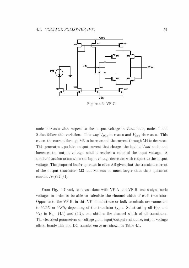
4.1. VOLTAGE FOLLOWER (VF) 51
Figure 4.6: VF-C.
node increases with respect to the output voltage in V out node, nodes 1 and
2 also follow this variation. This way VSG3 increases and VGS4 decreases. This
causes the current through M3 to increase and the current through M4 to decrease.
This generates a positive output current that charges the load at V out node, and
increases the output voltage, until it reaches a value of the input voltage. A
similar situation arises when the input voltage decreases with respect to the output
voltage. The proposed buffer operates in class-AB given that the transient current
of the output transistors M3 and M4 can be much larger than their quiescent
current Iref/2 [31].
From Fig. 4.7 and, as it was done with VF-A and VF-B, one assigns node
voltages in order to be able to calculate the channel width of each transistor.
Opposite to the VF-B, in this VF all substrate or bulk terminals are connected
to V DD or V SS, depending of the transistor type. Substituting all VGS and
VSG in Eq. (4.1) and (4.2), one obtains the channel width of all transistors.
The electrical parameters as voltage gain, input/output resistance, output voltage
offset, bandwidth and DC transfer curve are shown in Table 4.1.
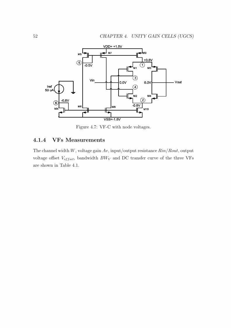
52 CHAPTER 4. UNITY GAIN CELLS (UGCS)
Figure 4.7: VF-C with node voltages.
4.1.4 VFs Measurements
The channel width W , voltage gain Av, input/output resistance Rin/Rout, output
voltage offset Voffset, bandwidth BWV and DC transfer curve of the three VFs
are shown in Table 4.1.
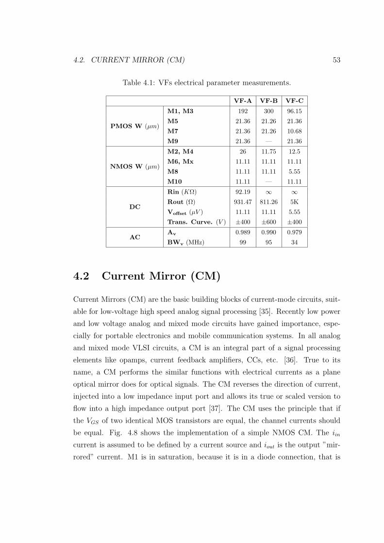
4.2. CURRENT MIRROR (CM) 53
Table 4.1: VFs electrical parameter measurements.
VF-A VF-B VF-C
PMOS W (µm)
M1, M3 192 300 96.15
M5 21.36 21.26 21.36
M7 21.36 21.26 10.68
M9 21.36 — 21.36
NMOS W (µm)
M2, M4 26 11.75 12.5
M6, Mx 11.11 11.11 11.11
M8 11.11 11.11 5.55
M10 11.11 — 11.11
DC
Rin (KΩ) 92.19 ∞ ∞Rout (Ω) 931.47 811.26 5K
Voffset (µV ) 11.11 11.11 5.55
Trans. Curve. (V ) ±400 ±600 ±400
ACAv 0.989 0.990 0.979
BWv (MHz) 99 95 34
4.2 Current Mirror (CM)
Current Mirrors (CM) are the basic building blocks of current-mode circuits, suit-
able for low-voltage high speed analog signal processing [35]. Recently low power
and low voltage analog and mixed mode circuits have gained importance, espe-
cially for portable electronics and mobile communication systems. In all analog
and mixed mode VLSI circuits, a CM is an integral part of a signal processing
elements like opamps, current feedback amplifiers, CCs, etc. [36]. True to its
name, a CM performs the similar functions with electrical currents as a plane
optical mirror does for optical signals. The CM reverses the direction of current,
injected into a low impedance input port and allows its true or scaled version to
flow into a high impedance output port [37]. The CM uses the principle that if
the VGS of two identical MOS transistors are equal, the channel currents should
be equal. Fig. 4.8 shows the implementation of a simple NMOS CM. The iin
current is assumed to be defined by a current source and iout is the output ”mir-
rored” current. M1 is in saturation, because it is in a diode connection, that is

54 CHAPTER 4. UNITY GAIN CELLS (UGCS)
VGS1 = VDS1 [21]. Assuming that VDS2 > (VGS2 − VTH2), is correct to use the
saturation region equation (Eq. (A.12)). The ratio of iout to iin is as follows:
iout
iin=
(L1W2
W1L2
)(VGS − VTH2
VGS − VTH1
)2 [1 + λVDS2
1 + λVDS1
(K2
K1
)](4.3)
All the components of a CM are processed on the same integrated circuit, so
all the physical parameters, such as VTH and K ′ are identical for both type of
devices. As a result, and if VDS2 = VDS1, the ratio of Eq. (4.3) can be simplified
by:
iout
iin=
L1W2
W1L2
(4.4)
So in Eq. (4.4), iout/iin is a function of the aspect ratios that are under designer
control.
Figure 4.8: NMOS Current Mirror.
4.2.1 Simple CM (SCM)
The simplest symmetrical CM is based on the circuit shown in Fig. 4.8, just
adding the same structure by PMOS transistors at the top of that circuit, to have

4.2. CURRENT MIRROR (CM) 55
the Simple symmetrical CM or Simple CM (SCM) shown in Fig. 4.9, which will
be used in this work. Substituting all VGS and VSG in Eq. (4.1) and (4.2), one
obtains the channel width of all transistors. The electrical parameters as current
gain, input/output resistance, output current offset, bandwidth and DC transfer
curve are shown in Table 4.2.
Figure 4.9: Simple Current Mirror.
4.2.2 Low Voltage CM (LVCM)
One of the most important disadvantages of the SCM is its poor output impedance
and linearity worsening with smaller channel length designs [38]. Now is presented
the commonly named Wide-swing or Low-voltage Cascode CM (LVCM) [38, 39,
40, 41, 42]. Its topology is shown in Fig. 4.10. In this work is not used the
very popular Cascode CM, because of the low value of the bias voltages (V DD
and V SS). On its place it was chosen the low voltage version of that CM. The
VDS1 and VDS2 are controlled by the gate of transistors M4 and M3, respectively.
So, the VDS1 and VDS2 are not equal to its VGS1 or VGS2 for each case. The
matching between these two elements ensure identical voltage at the drains of
these transistors (M1 and M2), leading to a systematic current matching. The
gates terminals of M3 and M4 are biased by a control voltage (V b) that maintain
both M1 and M2 in the saturation region. This voltage avoid M4 to move to the
triode region [43]. In order to agree with this, the voltages relations given by Eqs.
(4.5) and (4.6).
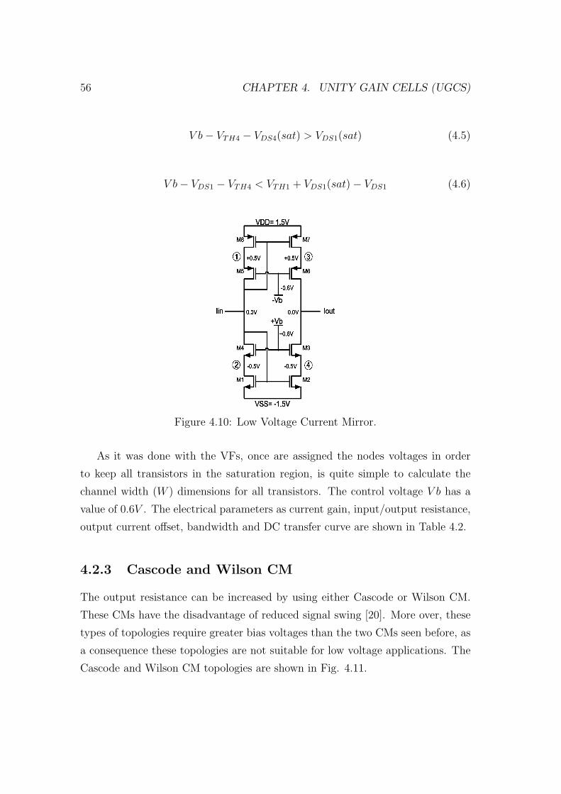
56 CHAPTER 4. UNITY GAIN CELLS (UGCS)
V b− VTH4 − VDS4(sat) > VDS1(sat) (4.5)
V b− VDS1 − VTH4 < VTH1 + VDS1(sat)− VDS1 (4.6)
Figure 4.10: Low Voltage Current Mirror.
As it was done with the VFs, once are assigned the nodes voltages in order
to keep all transistors in the saturation region, is quite simple to calculate the
channel width (W ) dimensions for all transistors. The control voltage V b has a
value of 0.6V . The electrical parameters as current gain, input/output resistance,
output current offset, bandwidth and DC transfer curve are shown in Table 4.2.
4.2.3 Cascode and Wilson CM
The output resistance can be increased by using either Cascode or Wilson CM.
These CMs have the disadvantage of reduced signal swing [20]. More over, these
types of topologies require greater bias voltages than the two CMs seen before, as
a consequence these topologies are not suitable for low voltage applications. The
Cascode and Wilson CM topologies are shown in Fig. 4.11.
4.2. CURRENT MIRROR (CM) 57
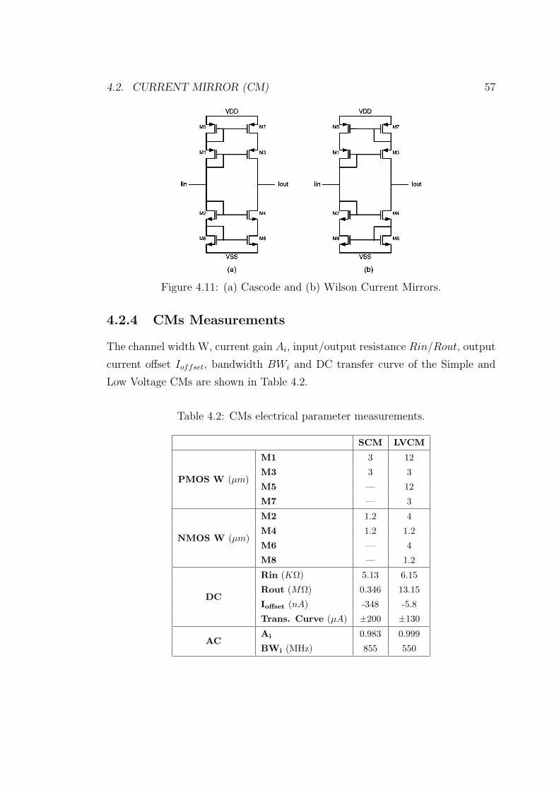
Figure 4.11: (a) Cascode and (b) Wilson Current Mirrors.
4.2.4 CMs Measurements
The channel width W, current gain Ai, input/output resistance Rin/Rout, output
current offset Ioffset, bandwidth BWi and DC transfer curve of the Simple and
Low Voltage CMs are shown in Table 4.2.
Table 4.2: CMs electrical parameter measurements.
SCM LVCM
PMOS W (µm)
M1 3 12
M3 3 3
M5 — 12
M7 — 3
NMOS W (µm)
M2 1.2 4
M4 1.2 1.2
M6 — 4
M8 — 1.2
DC
Rin (KΩ) 5.13 6.15
Rout (MΩ) 0.346 13.15
Ioffset (nA) -348 -5.8
Trans. Curve (µA) ±200 ±130
ACAi 0.983 0.999
BWi (MHz) 855 550
58 CHAPTER 4. UNITY GAIN CELLS (UGCS)
4.3 Voltage Mirror (VM)
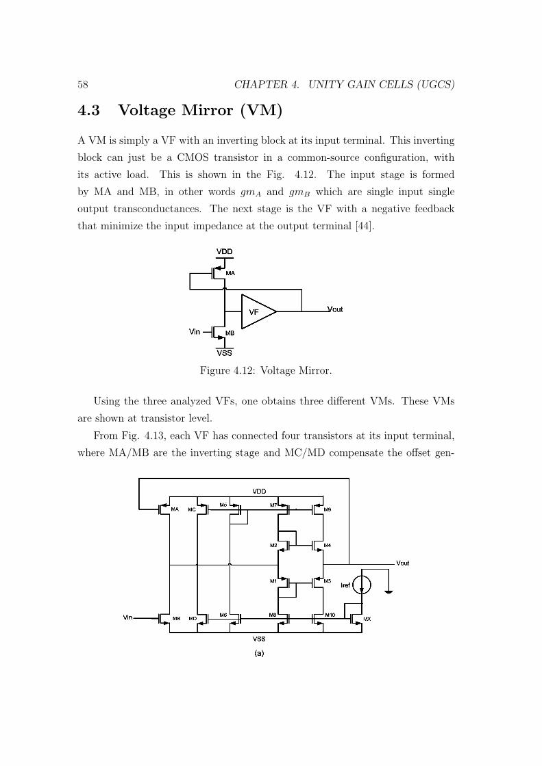
A VM is simply a VF with an inverting block at its input terminal. This inverting
block can just be a CMOS transistor in a common-source configuration, with
its active load. This is shown in the Fig. 4.12. The input stage is formed
by MA and MB, in other words gmA and gmB which are single input single
output transconductances. The next stage is the VF with a negative feedback
that minimize the input impedance at the output terminal [44].
Figure 4.12: Voltage Mirror.
Using the three analyzed VFs, one obtains three different VMs. These VMs
are shown at transistor level.
From Fig. 4.13, each VF has connected four transistors at its input terminal,
where MA/MB are the inverting stage and MC/MD compensate the offset gen-

4.3. VOLTAGE MIRROR (VM) 59
Figure 4.13: Voltage Mirror: (a) VM-A, (b) VM-B and (c) VM-C.
erated by MA and MB. The offset in the gates terminals of M1 and M2 is fixed
by the feedback between V out node and the gate terminal of MA. MC and MD
drain a current that generates a voltage in that node that compensates the fixed
offset. VM-B and VM-C have a capacitor named Cc in order to smooth the AC
response near the cut-off frequency. At this point, without Cc, VM-B and VM-C
present a peak of some units of dB, making these circuits unstable. The reason
is due to the connection of the inverted stage output with the M1 and M2 gates,
which represents a very high impedance at this point.
60 CHAPTER 4. UNITY GAIN CELLS (UGCS)
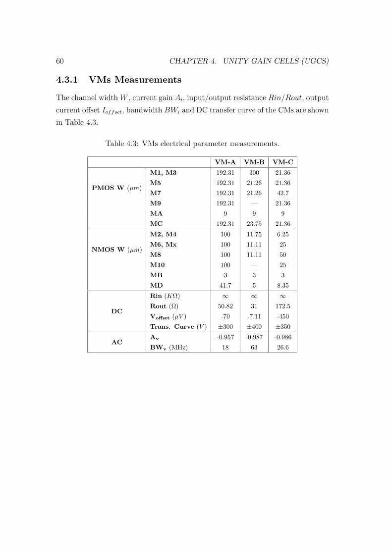
4.3.1 VMs Measurements
The channel width W , current gain Ai, input/output resistance Rin/Rout, output
current offset Ioffset, bandwidth BWi and DC transfer curve of the CMs are shown
in Table 4.3.
Table 4.3: VMs electrical parameter measurements.
VM-A VM-B VM-C
PMOS W (µm)
M1, M3 192.31 300 21.36
M5 192.31 21.26 21.36
M7 192.31 21.26 42.7
M9 192.31 — 21.36
MA 9 9 9
MC 192.31 23.75 21.36
NMOS W (µm)
M2, M4 100 11.75 6.25
M6, Mx 100 11.11 25
M8 100 11.11 50
M10 100 — 25
MB 3 3 3
MD 41.7 5 8.35
DC
Rin (KΩ) ∞ ∞ ∞Rout (Ω) 50.82 31 172.5
Voffset (µV ) -70 -7.11 -450
Trans. Curve (V ) ±300 ±400 ±350
ACAv -0.957 -0.987 -0.986
BWv (MHz) 18 63 26.6
4.4. CURRENT FOLLOWER (CF) 61
4.4 Current Follower (CF)
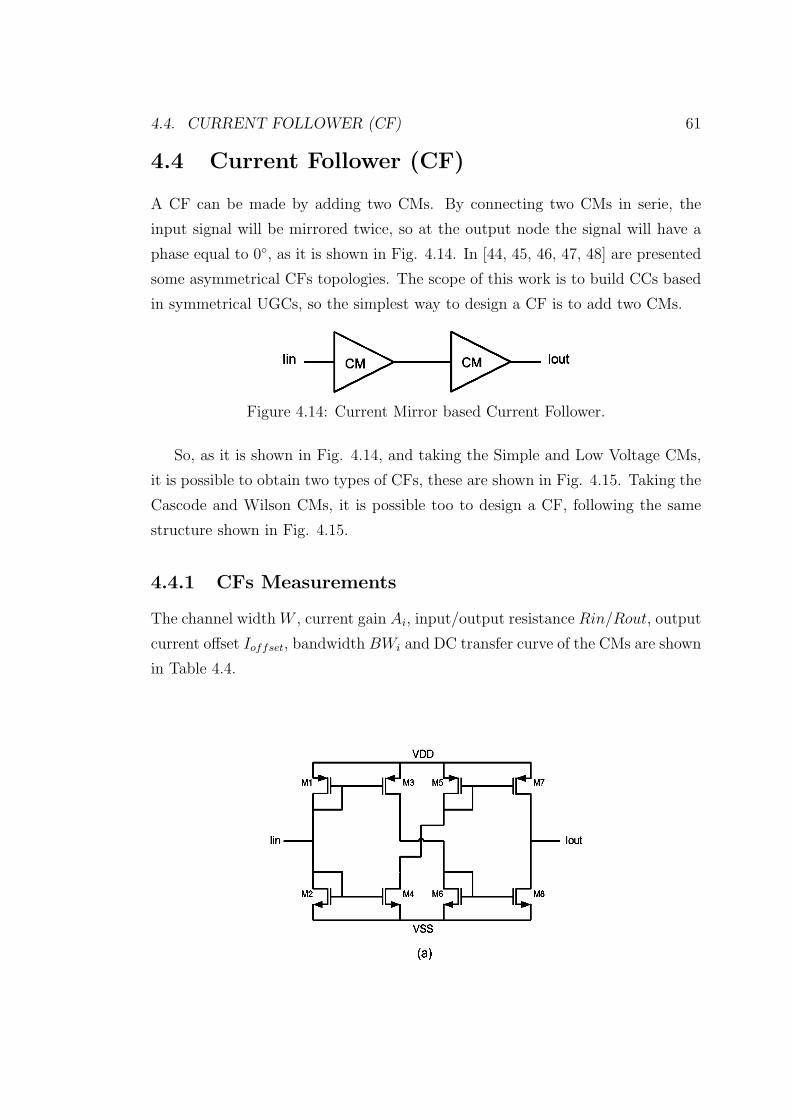
A CF can be made by adding two CMs. By connecting two CMs in serie, the
input signal will be mirrored twice, so at the output node the signal will have a
phase equal to 0, as it is shown in Fig. 4.14. In [44, 45, 46, 47, 48] are presented
some asymmetrical CFs topologies. The scope of this work is to build CCs based
in symmetrical UGCs, so the simplest way to design a CF is to add two CMs.
Figure 4.14: Current Mirror based Current Follower.
So, as it is shown in Fig. 4.14, and taking the Simple and Low Voltage CMs,
it is possible to obtain two types of CFs, these are shown in Fig. 4.15. Taking the
Cascode and Wilson CMs, it is possible too to design a CF, following the same
structure shown in Fig. 4.15.
4.4.1 CFs Measurements
The channel width W , current gain Ai, input/output resistance Rin/Rout, output
current offset Ioffset, bandwidth BWi and DC transfer curve of the CMs are shown
in Table 4.4.

62 CHAPTER 4. UNITY GAIN CELLS (UGCS)
Figure 4.15: (a) Simple and (b) Low Voltage Current Followers.
Table 4.4: CFs electrical parameter measurements.
SCF LVCF
PMOS W (µm)
M1, M3 3 12
M5, M7 3 3
M9, M11 — 12
M13, M15 — 3
NMOS W (µm)
M2, M4 1.23 4
M6, M8 1.23 1.2
M10, M12 — 4
M14, M16 — 1.2
DC
Rin (KΩ) 5.13 6.15
Rout (MΩ) 0.346 13.15
Ioffset (nA) -348 -5.8
Trans. Curve (µA) ±120 ±100
ACAi -0.954 -0.998
BWi (MHz) 478 345
Chapter 5
Direct and Inverse Current
Conveyors
The CC is a basic building block that can be implemented in analog circuit design.
It also represents an effective alternative to the opamps designers, due to the fact
that practical CCs are marked by characteristics that are very close to the ideal
one. More over, with the growing diffusion of the current-mode approach as a way
to design low-voltage low-power circuits, CCs have gained an increased popularity
[4].
In orther to classify all CCs, and since all CCs will be Dual-output type, they
will be named in the following order:
CC Type - VF or VM type - CM and CF type.
An example of the nomenclature will be:
DOCCI − V FA− S
It indicates a Dual-output First Generation CC, based in the VFA and Simple
CMs and CFs. In order to name a Dual-output Third Generation CC, VFC and
Low Voltage CMs and CFs based, the nomenclature will be:
DOCCIII − V FC − LV
63

64 CHAPTER 5. DIRECT AND INVERSE CURRENT CONVEYORS
5.1 Direct Current Conveyors
5.1.1 Direct First Generation Current Conveyor (CCI)
The behavior and structure of the CCI was described in Chapter 2 by Eq. (2.1)
and Fig. 2.2, respectively. In order to implement a CCI with a CMOS transistor-
based circuit, it is necessary to join a VF with two CMs (CCI+) or a VF with a
CM and a CF (CCI-). A Double-output CCI (DOCCI) block structure is shown
in Fig. 5.1, which is based in the VF-A. Of course, it can be based in the VF-B
or VF-C circuits.
Figure 5.1: DOCCI structure.
Where, in Fig. 5.1, CMINPand CMINN
are formed by M5/M7 and M6/M8
respectively, and its purpose is to bias the VF. CM1P and CM1N are the first
Current Mirror for iy = ix. CM2P and CM2N are the second Current Mirror for
iz = ix. Finally CF1P and CF1N are the first Current Follower for iz = −ix.
For a complete transistor level, in Fig. 5.2 is shown a DOCCI based in the VFA,
SCM and SCF, where CM1P and CM1N is formed by M9/M11 and M10/M12,
respectively. CM2P and CM2N is formed by M9/M13 and M10/M14, respectively.
Finally CF1P and CF1N is formed by M9/M15/M17/M19 and M10/M16/M18/M20,
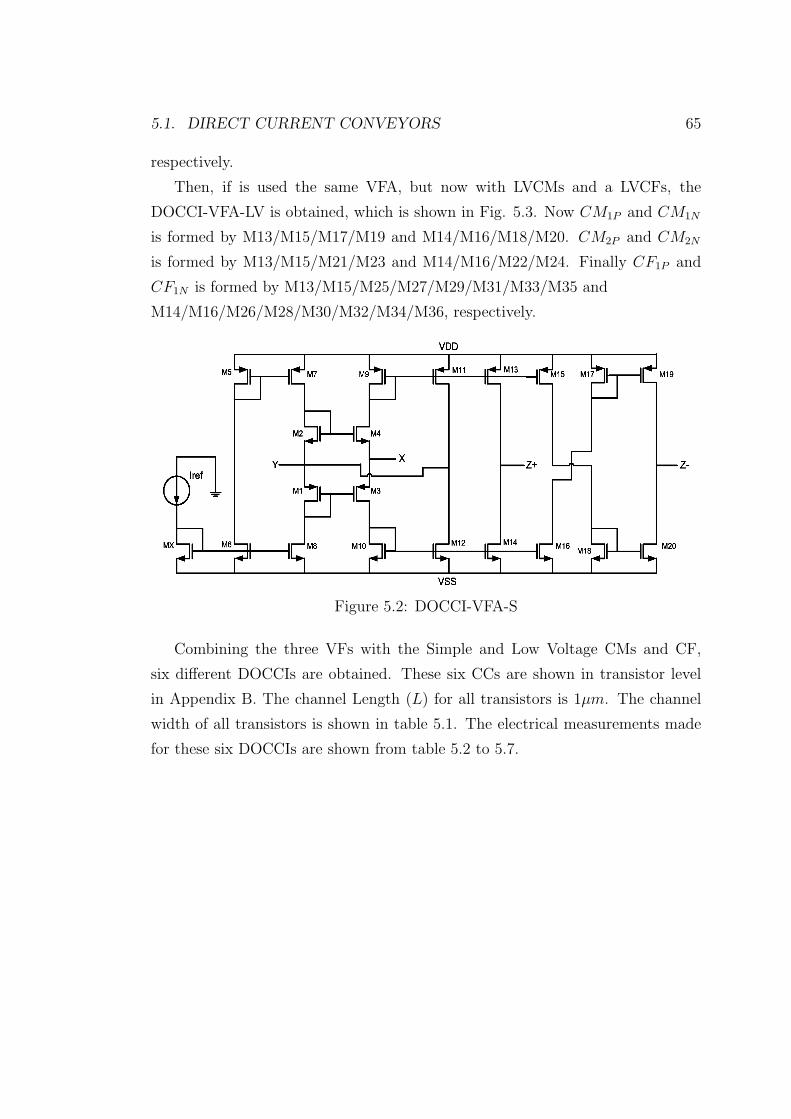
5.1. DIRECT CURRENT CONVEYORS 65
respectively.
Then, if is used the same VFA, but now with LVCMs and a LVCFs, the
DOCCI-VFA-LV is obtained, which is shown in Fig. 5.3. Now CM1P and CM1N
is formed by M13/M15/M17/M19 and M14/M16/M18/M20. CM2P and CM2N
is formed by M13/M15/M21/M23 and M14/M16/M22/M24. Finally CF1P and
CF1N is formed by M13/M15/M25/M27/M29/M31/M33/M35 and
M14/M16/M26/M28/M30/M32/M34/M36, respectively.
Figure 5.2: DOCCI-VFA-S
Combining the three VFs with the Simple and Low Voltage CMs and CF,
six different DOCCIs are obtained. These six CCs are shown in transistor level
in Appendix B. The channel Length (L) for all transistors is 1µm. The channel
width of all transistors is shown in table 5.1. The electrical measurements made
for these six DOCCIs are shown from table 5.2 to 5.7.

66 CHAPTER 5. DIRECT AND INVERSE CURRENT CONVEYORS
Figure 5.3: DOCCI-VFA-LV
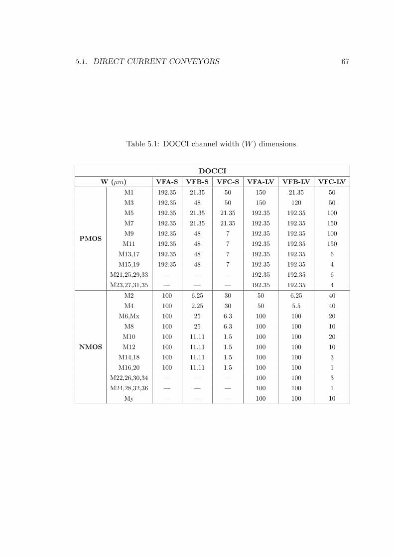
5.1. DIRECT CURRENT CONVEYORS 67
Table 5.1: DOCCI channel width (W ) dimensions.
DOCCIW (µm) VFA-S VFB-S VFC-S VFA-LV VFB-LV VFC-LV
PMOS
M1 192.35 21.35 50 150 21.35 50
M3 192.35 48 50 150 120 50
M5 192.35 21.35 21.35 192.35 192.35 100
M7 192.35 21.35 21.35 192.35 192.35 150
M9 192.35 48 7 192.35 192.35 100
M11 192.35 48 7 192.35 192.35 150
M13,17 192.35 48 7 192.35 192.35 6
M15,19 192.35 48 7 192.35 192.35 4
M21,25,29,33 — — — 192.35 192.35 6
M23,27,31,35 — — — 192.35 192.35 4
NMOS
M2 100 6.25 30 50 6.25 40
M4 100 2.25 30 50 5.5 40
M6,Mx 100 25 6.3 100 100 20
M8 100 25 6.3 100 100 10
M10 100 11.11 1.5 100 100 20
M12 100 11.11 1.5 100 100 10
M14,18 100 11.11 1.5 100 100 3
M16,20 100 11.11 1.5 100 100 1
M22,26,30,34 — — — 100 100 3
M24,28,32,36 — — — 100 100 1
My — — — 100 100 10
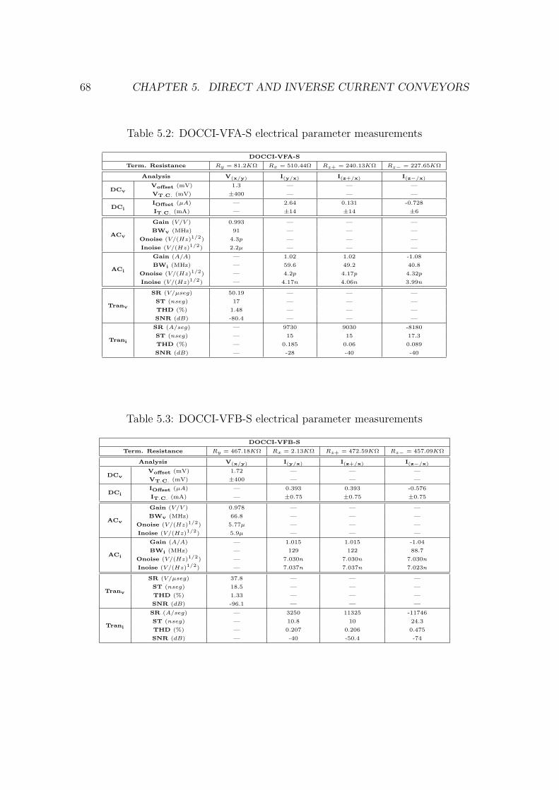
68 CHAPTER 5. DIRECT AND INVERSE CURRENT CONVEYORS
Table 5.2: DOCCI-VFA-S electrical parameter measurements
DOCCI-VFA-S
Term. Resistance Ry = 81.2KΩ Rx = 510.44Ω Rz+ = 240.13KΩ Rz− = 227.65KΩ
Analysis V(x/y) I(y/x) I(z+/x) I(z−/x)
DCvVoffset (mV) 1.3 — — —
VT.C. (mV) ±400 — — —
DCiIOffset (µA) — 2.64 0.131 -0.728
IT.C. (mA) — ±14 ±14 ±6
ACv
Gain (V/V ) 0.993 — — —
BWv (MHz) 91 — — —
Onoise (V/(Hz)1/2) 4.3p — — —
Inoise (V/(Hz)1/2) 2.2µ — — —
ACi
Gain (A/A) — 1.02 1.02 -1.08
BWi (MHz) — 59.6 49.2 40.8
Onoise (V/(Hz)1/2) — 4.2p 4.17p 4.32p
Inoise (V/(Hz)1/2) — 4.17n 4.06n 3.99n
Tranv
SR (V/µseg) 50.19 — — —
ST (nseg) 17 — — —
THD (%) 1.48 — — —
SNR (dB) -80.4 — — —
Trani
SR (A/seg) — 9730 9030 -8180
ST (nseg) — 15 15 17.3
THD (%) — 0.185 0.06 0.089
SNR (dB) — -28 -40 -40
Table 5.3: DOCCI-VFB-S electrical parameter measurements
DOCCI-VFB-S
Term. Resistance Ry = 467.18KΩ Rx = 2.13KΩ Rz+ = 472.59KΩ Rz− = 457.09KΩ
Analysis V(x/y) I(y/x) I(z+/x) I(z−/x)
DCvVoffset (mV) 1.72 — — —
VT.C. (mV) ±400 — — —
DCiIOffset (µA) — 0.393 0.393 -0.576
IT.C. (mA) — ±0.75 ±0.75 ±0.75
ACv
Gain (V/V ) 0.978 — — —
BWv (MHz) 66.8 — — —
Onoise (V/(Hz)1/2) 5.77µ — — —
Inoise (V/(Hz)1/2) 5.9µ — — —
ACi
Gain (A/A) — 1.015 1.015 -1.04
BWi (MHz) — 129 122 88.7
Onoise (V/(Hz)1/2) — 7.030n 7.030n 7.030n
Inoise (V/(Hz)1/2) — 7.037n 7.037n 7.023n
Tranv
SR (V/µseg) 37.8 — — —
ST (nseg) 18.5 — — —
THD (%) 1.33 — — —
SNR (dB) -96.1 — — —
Trani
SR (A/seg) — 3250 11325 -11746
ST (nseg) — 10.8 10 24.3
THD (%) — 0.207 0.206 0.475
SNR (dB) — -40 -50.4 -74
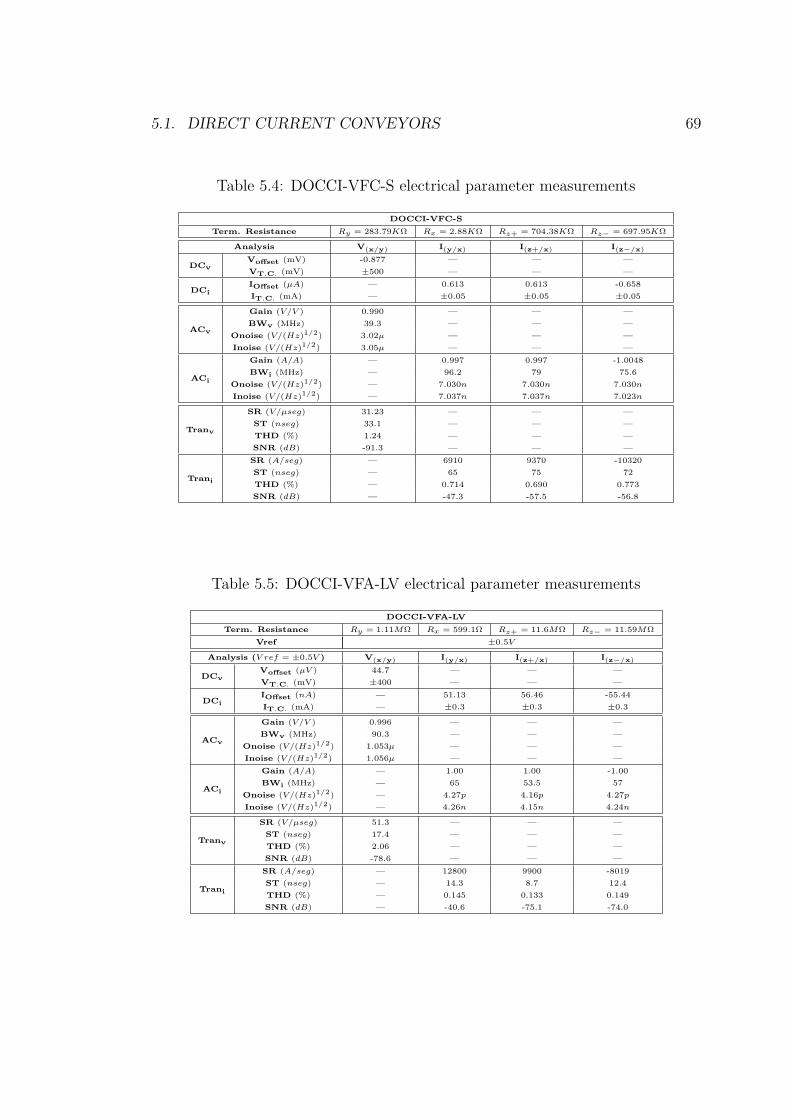
5.1. DIRECT CURRENT CONVEYORS 69
Table 5.4: DOCCI-VFC-S electrical parameter measurements
DOCCI-VFC-S
Term. Resistance Ry = 283.79KΩ Rx = 2.88KΩ Rz+ = 704.38KΩ Rz− = 697.95KΩ
Analysis V(x/y) I(y/x) I(z+/x) I(z−/x)
DCvVoffset (mV) -0.877 — — —
VT.C. (mV) ±500 — — —
DCiIOffset (µA) — 0.613 0.613 -0.658
IT.C. (mA) — ±0.05 ±0.05 ±0.05
ACv
Gain (V/V ) 0.990 — — —
BWv (MHz) 39.3 — — —
Onoise (V/(Hz)1/2) 3.02µ — — —
Inoise (V/(Hz)1/2) 3.05µ — — —
ACi
Gain (A/A) — 0.997 0.997 -1.0048
BWi (MHz) — 96.2 79 75.6
Onoise (V/(Hz)1/2) — 7.030n 7.030n 7.030n
Inoise (V/(Hz)1/2) — 7.037n 7.037n 7.023n
Tranv
SR (V/µseg) 31.23 — — —
ST (nseg) 33.1 — — —
THD (%) 1.24 — — —
SNR (dB) -91.3 — — —
Trani
SR (A/seg) — 6910 9370 -10320
ST (nseg) — 65 75 72
THD (%) — 0.714 0.690 0.773
SNR (dB) — -47.3 -57.5 -56.8
Table 5.5: DOCCI-VFA-LV electrical parameter measurements
DOCCI-VFA-LV
Term. Resistance Ry = 1.11MΩ Rx = 599.1Ω Rz+ = 11.6MΩ Rz− = 11.59MΩ
Vref ±0.5V
Analysis (V ref = ±0.5V ) V(x/y) I(y/x) I(z+/x) I(z−/x)
DCvVoffset (µV ) 44.7 — — —
VT.C. (mV) ±400 — — —
DCiIOffset (nA) — 51.13 56.46 -55.44
IT.C. (mA) — ±0.3 ±0.3 ±0.3
ACv
Gain (V/V ) 0.996 — — —
BWv (MHz) 90.3 — — —
Onoise (V/(Hz)1/2) 1.053µ — — —
Inoise (V/(Hz)1/2) 1.056µ — — —
ACi
Gain (A/A) — 1.00 1.00 -1.00
BWi (MHz) — 65 53.5 57
Onoise (V/(Hz)1/2) — 4.27p 4.16p 4.27p
Inoise (V/(Hz)1/2) — 4.26n 4.15n 4.24n
Tranv
SR (V/µseg) 51.3 — — —
ST (nseg) 17.4 — — —
THD (%) 2.06 — — —
SNR (dB) -78.6 — — —
Trani
SR (A/seg) — 12800 9900 -8019
ST (nseg) — 14.3 8.7 12.4
THD (%) — 0.145 0.133 0.149
SNR (dB) — -40.6 -75.1 -74.0
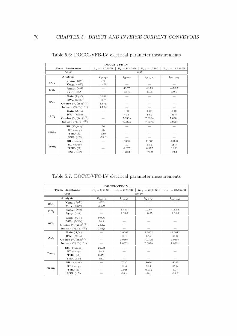
70 CHAPTER 5. DIRECT AND INVERSE CURRENT CONVEYORS
Table 5.6: DOCCI-VFB-LV electrical parameter measurements
DOCCI-VFB-LV
Term. Resistance Ry = 11.25MΩ Rx = 841.02Ω Rz+ = 12MΩ Rz− = 11.98MΩ
Vref ±0.4V
Analysis V(x/y) I(y/x) I(z+/x) I(z−/x)
DCvVoffset (µV ) 771 — — —
VT.C. (mV) ±400 — — —
DCiIOffset (nA) — 43.75 43.75 -47.92
IT.C. (mA) — ±0.5 ±0.5 ±0.5
ACv
Gain (V/V ) 0.989 — — —
BWv (MHz) 86.7 — — —
Onoise (V/(Hz)1/2) 4.67µ — — —
Inoise (V/(Hz)1/2) 4.72µ — — —
ACi
Gain (A/A) — 1.00 1.00 -1.00
BWi (MHz) — 89.6 88.2 86.8
Onoise (V/(Hz)1/2) — 7.030n 7.030n 7.030n
Inoise (V/(Hz)1/2) — 7.037n 7.037n 7.023n
Tranv
SR (V/µseg) 56 — — —
ST (nseg) 25 — — —
THD (%) 0.89 — — —
SNR (dB) -78.0 — — —
Trani
SR (A/seg) — 8390 11300 -10147
ST (nseg) — 10 15.4 18.3
THD (%) — 0.075 0.077 0.123
SNR (dB) — -72.3 -74.2 -72.4
Table 5.7: DOCCI-VFC-LV electrical parameter measurements
DOCCI-VFC-LV
Term. Resistance Ry = 8.64MΩ Rx = 2.74KΩ Rz+ = 23.93MΩ Rz− = 23.86MΩ
Vref ±0.4V
Analysis V(x/y) I(y/x) I(z+/x) I(z−/x)
DCvVoffset (µV ) -223 — — —
VT.C. (mV) ±500 — — —
DCiIOffset (nA) — 13.53 10.07 -13.53
IT.C. (mA) — ±0.05 ±0.05 ±0.05
ACv
Gain (V/V ) 0.996 — — —
BWv (MHz) 38.2 — — —
Onoise (V/(Hz)1/2) 2.51µ — — —
Inoise (V/(Hz)1/2) 2.53µ — — —
ACi
Gain (A/A) — 1.0002 1.0002 -1.0012
BWi (MHz) — 83.1 67.2 66.8
Onoise (V/(Hz)1/2) — 7.030n 7.030n 7.030n
Inoise (V/(Hz)1/2) — 7.037n 7.037n 7.023n
Tranv
SR (V/µseg) 26.92 — — —
ST (nseg) 38.3 — — —
THD (%) 0.651 — — —
SNR (dB) -88.1 — — —
Trani
SR (A/seg) — 7630 8096 -8395
ST (nseg) — 88.4 91.7 85.5
THD (%) — 0.938 0.912 1.07
SNR (dB) — -58.4 -56.1 -55.3
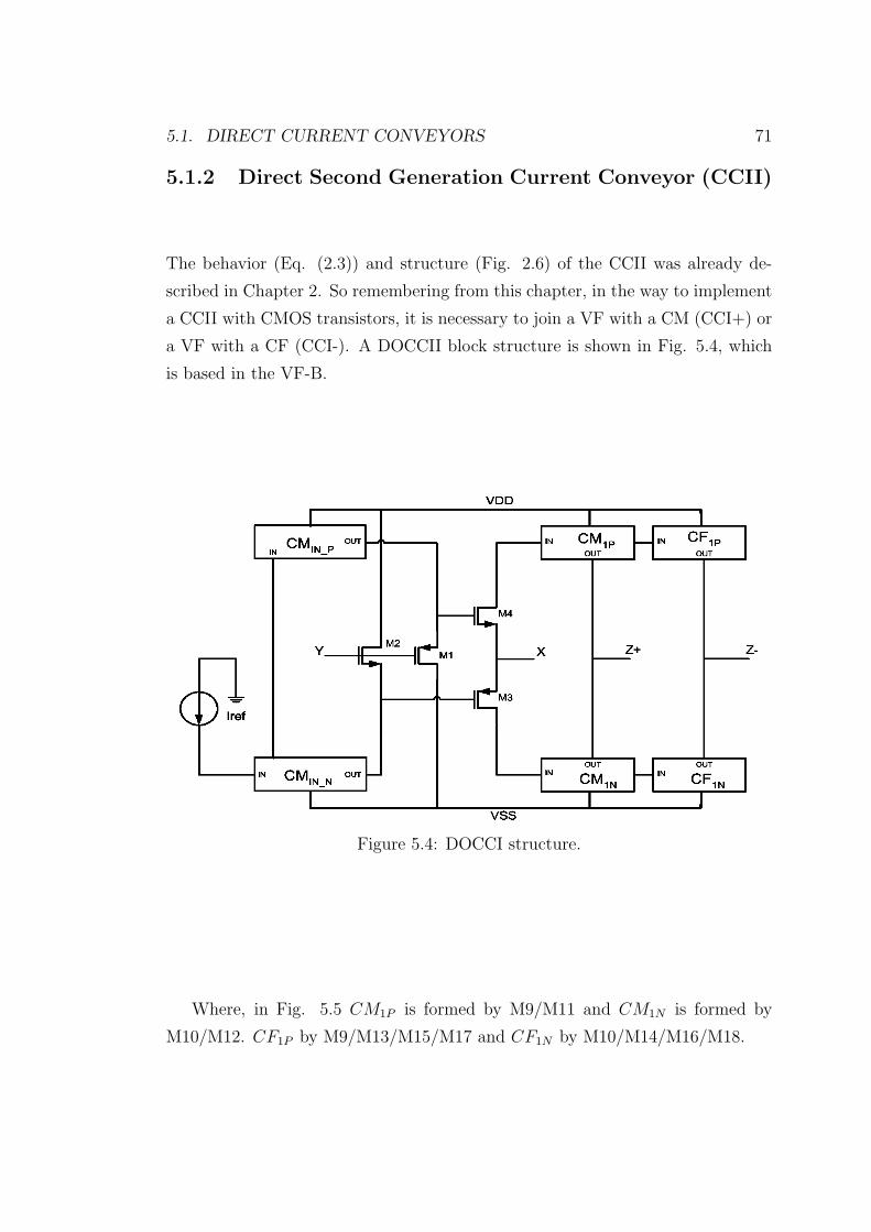
5.1. DIRECT CURRENT CONVEYORS 71
5.1.2 Direct Second Generation Current Conveyor (CCII)
The behavior (Eq. (2.3)) and structure (Fig. 2.6) of the CCII was already de-
scribed in Chapter 2. So remembering from this chapter, in the way to implement
a CCII with CMOS transistors, it is necessary to join a VF with a CM (CCI+) or
a VF with a CF (CCI-). A DOCCII block structure is shown in Fig. 5.4, which
is based in the VF-B.
Figure 5.4: DOCCI structure.
Where, in Fig. 5.5 CM1P is formed by M9/M11 and CM1N is formed by
M10/M12. CF1P by M9/M13/M15/M17 and CF1N by M10/M14/M16/M18.

72 CHAPTER 5. DIRECT AND INVERSE CURRENT CONVEYORS
Figure 5.5: DOCCII-VFB-S
Again, combining the three VFs with both CMs and CFs (simple and low
voltage), is possible to obtain six DOCCIIs, which are shown in Appendix B
in transistor level. As the DOCCIs, the channel length (L) is equal to 1µm.
The channel width (W ) of all DOCCIIs transistors are shown in table 5.8. The
electrical parameter measurements of these CCCs are shown from table 5.9 to 5.14

5.1. DIRECT CURRENT CONVEYORS 73
Table 5.8: DOCCII channel width (W ) dimensions.
DOCCIIW (µm) VFA-S VFB-S VFC-S VFA-LV VFB-LV VFC-LV
PMOS
M1 192.35 21.35 50 192.35 21.35 50
M3 192.35 48 50 192.35 120 50
M5 192.35 21.35 21.35 192.35 192.35 100
M7 192.35 21.35 21.35 192.35 192.35 150
M9 192.35 48 7 192.35 192.35 100
M11 192.35 48 7 192.35 192.35 150
M13,17 192.35 48 7 192.35 192.35 6
M15 192.35 48 7 192.35 192.35 4
M21,25,29 — — — 192.35 192.35 6
M19,23,27,31 — — — 192.35 192.35 4
NMOS
M2 100 6.25 30 100 6.25 40
M4 100 2.25 30 100 5.5 40
M6,Mx 100 25 6.3 100 100 20
M8 100 25 6.3 100 100 10
M10 100 11.11 1.5 100 100 20
M12 100 11.11 1.5 100 100 10
M14,18 100 11.11 1.5 100 100 3
M16 100 11.11 1.5 100 100 1
M22,26,30 — — — 100 100 3
M20,24,28,32 — — — 100 100 1
My — — — 100 100 10
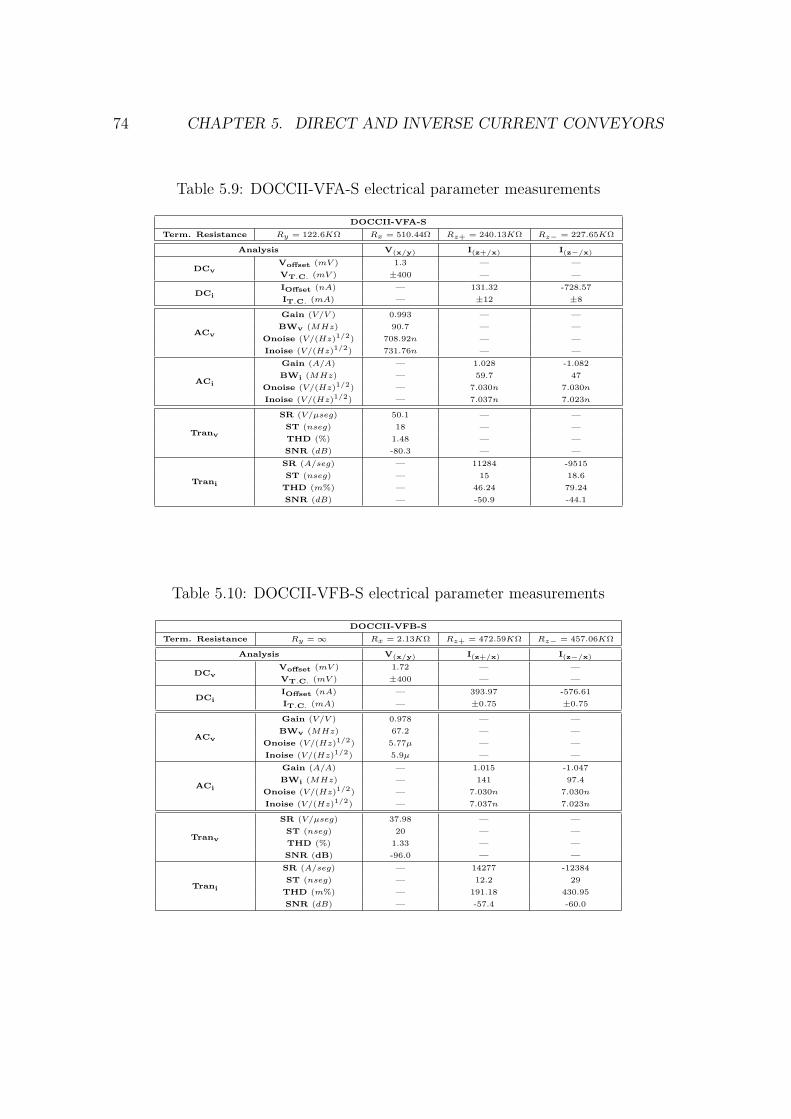
74 CHAPTER 5. DIRECT AND INVERSE CURRENT CONVEYORS
Table 5.9: DOCCII-VFA-S electrical parameter measurements
DOCCII-VFA-S
Term. Resistance Ry = 122.6KΩ Rx = 510.44Ω Rz+ = 240.13KΩ Rz− = 227.65KΩ
Analysis V(x/y) I(z+/x) I(z−/x)
DCvVoffset (mV ) 1.3 — —
VT.C. (mV ) ±400 — —
DCiIOffset (nA) — 131.32 -728.57
IT.C. (mA) — ±12 ±8
ACv
Gain (V/V ) 0.993 — —
BWv (MHz) 90.7 — —
Onoise (V/(Hz)1/2) 708.92n — —
Inoise (V/(Hz)1/2) 731.76n — —
ACi
Gain (A/A) — 1.028 -1.082
BWi (MHz) — 59.7 47
Onoise (V/(Hz)1/2) — 7.030n 7.030n
Inoise (V/(Hz)1/2) — 7.037n 7.023n
Tranv
SR (V/µseg) 50.1 — —
ST (nseg) 18 — —
THD (%) 1.48 — —
SNR (dB) -80.3 — —
Trani
SR (A/seg) — 11284 -9515
ST (nseg) — 15 18.6
THD (m%) — 46.24 79.24
SNR (dB) — -50.9 -44.1
Table 5.10: DOCCII-VFB-S electrical parameter measurements
DOCCII-VFB-S
Term. Resistance Ry = ∞ Rx = 2.13KΩ Rz+ = 472.59KΩ Rz− = 457.06KΩ
Analysis V(x/y) I(z+/x) I(z−/x)
DCvVoffset (mV ) 1.72 — —
VT.C. (mV ) ±400 — —
DCiIOffset (nA) — 393.97 -576.61
IT.C. (mA) — ±0.75 ±0.75
ACv
Gain (V/V ) 0.978 — —
BWv (MHz) 67.2 — —
Onoise (V/(Hz)1/2) 5.77µ — —
Inoise (V/(Hz)1/2) 5.9µ — —
ACi
Gain (A/A) — 1.015 -1.047
BWi (MHz) — 141 97.4
Onoise (V/(Hz)1/2) — 7.030n 7.030n
Inoise (V/(Hz)1/2) — 7.037n 7.023n
Tranv
SR (V/µseg) 37.98 — —
ST (nseg) 20 — —
THD (%) 1.33 — —
SNR (dB) -96.0 — —
Trani
SR (A/seg) — 14277 -12384
ST (nseg) — 12.2 29
THD (m%) — 191.18 430.95
SNR (dB) — -57.4 -60.0
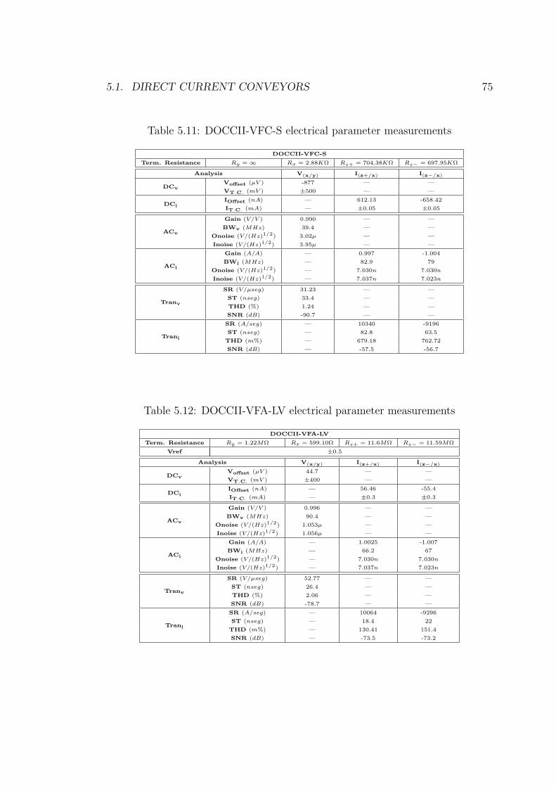
5.1. DIRECT CURRENT CONVEYORS 75
Table 5.11: DOCCII-VFC-S electrical parameter measurements
DOCCII-VFC-S
Term. Resistance Ry = ∞ Rx = 2.88KΩ Rz+ = 704.38KΩ Rz− = 697.95KΩ
Analysis V(x/y) I(z+/x) I(z−/x)
DCvVoffset (µV ) -877 — —
VT.C. (mV ) ±500 — —
DCiIOffset (nA) — 612.13 -658.42
IT.C. (mA) — ±0.05 ±0.05
ACv
Gain (V/V ) 0.990 — —
BWv (MHz) 39.4 — —
Onoise (V/(Hz)1/2) 3.02µ — —
Inoise (V/(Hz)1/2) 3.95µ — —
ACi
Gain (A/A) — 0.997 -1.004
BWi (MHz) — 82.9 79
Onoise (V/(Hz)1/2) — 7.030n 7.030n
Inoise (V/(Hz)1/2) — 7.037n 7.023n
Tranv
SR (V/µseg) 31.23 — —
ST (nseg) 33.4 — —
THD (%) 1.24 — —
SNR (dB) -90.7 — —
Trani
SR (A/seg) — 10340 -9196
ST (nseg) — 82.8 63.5
THD (m%) — 679.18 762.72
SNR (dB) — -57.5 -56.7
Table 5.12: DOCCII-VFA-LV electrical parameter measurements
DOCCII-VFA-LV
Term. Resistance Ry = 1.22MΩ Rx = 599.10Ω Rz+ = 11.6MΩ Rz− = 11.59MΩ
Vref ±0.5
Analysis V(x/y) I(z+/x) I(z−/x)
DCvVoffset (µV ) 44.7 — —
VT.C. (mV ) ±400 — —
DCiIOffset (nA) — 56.46 -55.4
IT.C. (mA) — ±0.3 ±0.3
ACv
Gain (V/V ) 0.996 — —
BWv (MHz) 90.4 — —
Onoise (V/(Hz)1/2) 1.053µ — —
Inoise (V/(Hz)1/2) 1.056µ — —
ACi
Gain (A/A) — 1.0025 -1.007
BWi (MHz) — 66.2 67
Onoise (V/(Hz)1/2) — 7.030n 7.030n
Inoise (V/(Hz)1/2) — 7.037n 7.023n
Tranv
SR (V/µseg) 52.77 — —
ST (nseg) 26.4 — —
THD (%) 2.06 — —
SNR (dB) -78.7 — —
Trani
SR (A/seg) — 10064 -9296
ST (nseg) — 18.4 22
THD (m%) — 130.41 151.4
SNR (dB) — -73.5 -73.2

76 CHAPTER 5. DIRECT AND INVERSE CURRENT CONVEYORS
Table 5.13: DOCCII-VFB-LV electrical parameter measurements
DOCCII-VFB-LV
Term. Resistance Ry = ∞ Rx = 841.02Ω Rz+ = 12MΩ Rz− = 11.98MΩ
Vref ±0.4
Analysis V(x/y) I(z+/x) I(z−/x)
DCvVoffset(µV ) 771.43 — —
VT.C. (mV ) ±400 — —
DCiIOffset (nA) — 43.75 -47.92
IT.C. (mA) — ±0.5 ±0.4
ACv
Gain (V/V ) 0.989 — —
BWv (MHz) 87.3 — —
Onoise (V/(Hz)1/2) 4.67µ — —
Inoise (V/(Hz)1/2) 4.72µ — —
ACi
Gain (A/A) — 1.0007 -1.0031
BWi (MHz) — 105 97.4
Onoise (V/(Hz)1/2) — 7.030n 7.030n
Inoise (V/(Hz)1/2) — 7.037n 7.023n
Tranv
SR (V/µseg) 56.43 — —
ST (nseg) 29.4 — —
THD (%) 0.89 — —
SNR (dB) -78.5 — —
Trani
SR (A/seg) — 14132 -11135
ST (nseg) — 10.4 17.7
THD (m%) — 47.5 105.76
SNR (dB) — -75.0 -72.9
Table 5.14: DOCCII-VFC-LV electrical parameter measurements
DOCCII-VFC-LV
Term. Resistance Ry = ∞ Rx = 2.74KΩ Rz+ = 23.93MΩ Rz− = 23.86MΩ
Vref ±0.4
Analysis V(x/y) I(z+/x) I(z−/x)
DCvVoffset (µV ) -223.4 — —
VT.C. (mV ) ±500 — —
DCiIOffset (nA) — 13.53 -10.07
IT.C. (mA) — ±0.05 ±0.05
ACv
Gain (V/V ) 0.996 — —
BWv (MHz) 38.1 — —
Onoise (V/(Hz)1/2) 2.51µ — —
Inoise (V/(Hz)1/2) 2.52µ — —
ACi
Gain (A/A) — 1.0002 -1.0012
BWi (MHz) — 69.8 69
Onoise (V/(Hz)1/2) — 7.030n 7.030n
Inoise (V/(Hz)1/2) — 7.037n 7.023n
Tranv
SR (V/µseg) 26.92 — —
ST (nseg) 39.2 — —
THD (%) 0.651 — —
SNR (dB) -87.5 — —
Trani
SR (A/seg) — 6689 -6501
ST (nseg) — 96.8 92.7
THD (%) — 0.902 1.06
SNR (dB) — -56.1 -55.2

5.1. DIRECT CURRENT CONVEYORS 77
5.1.3 Direct Third Generation Current Conveyor (CCIII)
As it was seen in Chapter 2, where the behavior and structure of the CCIII was
described by Eq. (2.5) and Fig. 2.10 respectively, in order to implement a CCIII
is necessary to join a VF with a CM and a CF (CCIII+) or a VF with two CFs
(CCIII-). A DOCCIII block structure is shown in Fig. 5.6, which is based in the
VF-C.
Figure 5.6: DOCCIII structure.
From Fig. 5.6, CM1P and CM1N are the first Current Mirror for iz+ = ix.
CF1P and CF1N are the first Current Follower for iz− = −ix. Finally CF2P and
CF2N are the second Current Follower for iy = −ix.
In Fig. 5.7 is shown a DOCCIII-VFC-SCM, where CM1P and CM1N are
formed by M9/M11 and M10/M12. CF1P and CF1N are formed by M9/M13/M15/M17
and M10/M14/M16/M18. Finally CF2P and CF2N are formed by M9/M13M15/M19
and M10/M14/M16/M20.
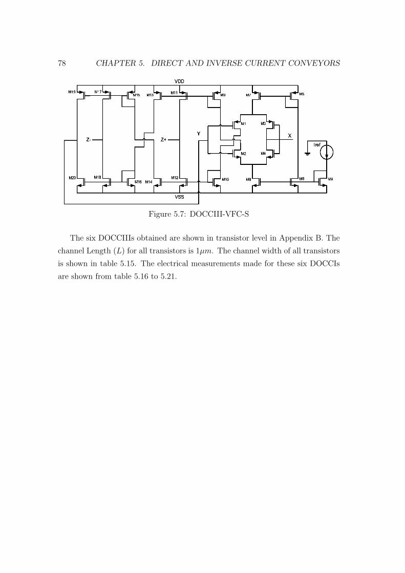
78 CHAPTER 5. DIRECT AND INVERSE CURRENT CONVEYORS
Figure 5.7: DOCCIII-VFC-S
The six DOCCIIIs obtained are shown in transistor level in Appendix B. The
channel Length (L) for all transistors is 1µm. The channel width of all transistors
is shown in table 5.15. The electrical measurements made for these six DOCCIs
are shown from table 5.16 to 5.21.

5.1. DIRECT CURRENT CONVEYORS 79
Table 5.15: DOCCIII channel width (W ) dimensions.
DOCCIIIW (µm) VFA-S VFB-S VFC-S VFA-LV VFB-LV VFC-LV
PMOS
M1 192.35 21.35 50 192.35 21.35 50
M3 192.35 48 50 192.35 120 50
M5 192.35 21.35 21.35 192.35 192.35 100
M7 192.35 21.35 21.35 192.35 192.35 150
M9 192.35 48 7 192.35 192.35 100
M11 192.35 48 7 192.35 192.35 150
M13,17 192.35 48 7 192.35 192.35 6
M15,19 192.35 48 7 192.35 192.35 4
M21,25,29,33 — — — 192.35 192.35 6
M23,27,31,35 — — — 192.35 192.35 4
NMOS
M2 100 6.25 30 100 6.25 40
M4 100 2.25 30 100 5.5 40
M6,Mx 100 25 6.3 100 100 20
M8 100 25 6.3 100 100 10
M10 100 11.11 1.5 100 100 20
M12 100 11.11 1.5 100 100 10
M14,18 100 11.11 1.5 100 100 3
M16,20 100 11.11 1.5 100 100 1
M22,26,30,34 — — — 100 100 3
M24,28,32,36 — — — 100 100 1
My — — — 100 100 10
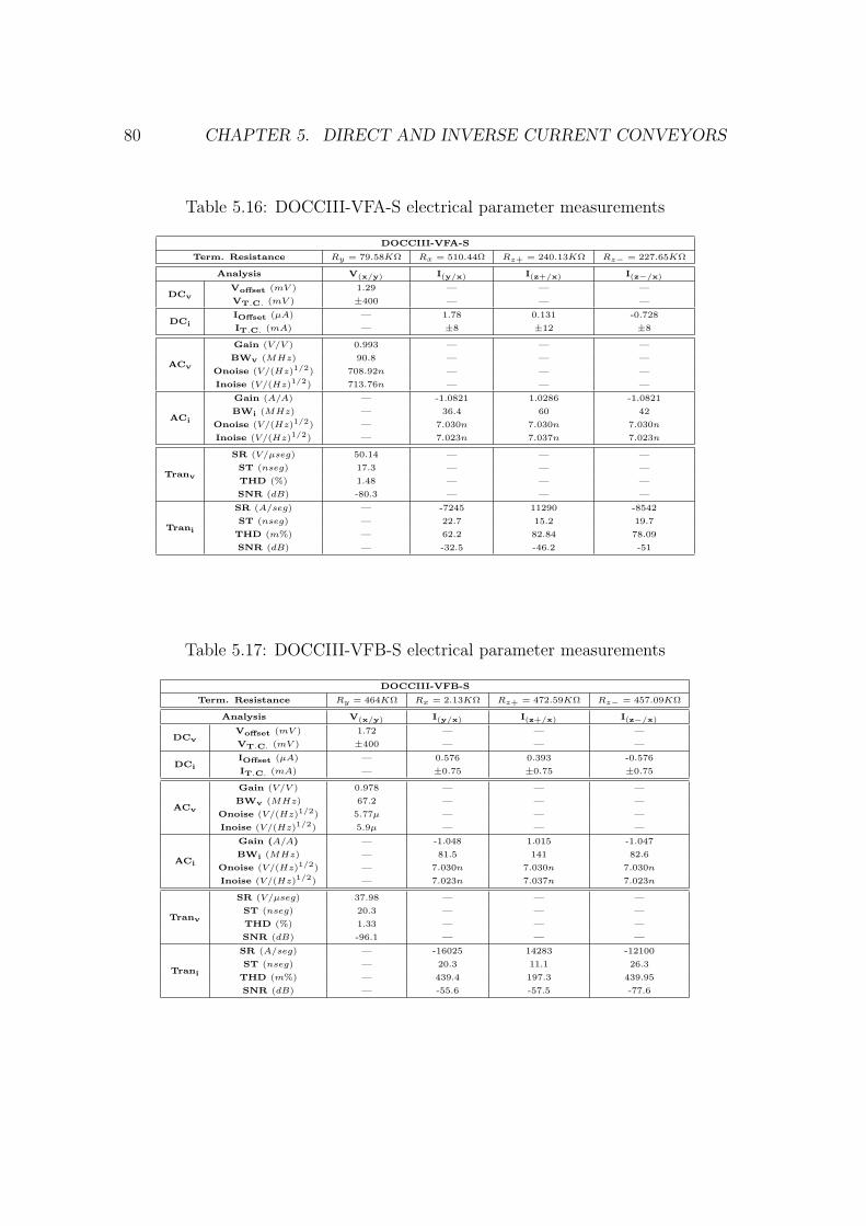
80 CHAPTER 5. DIRECT AND INVERSE CURRENT CONVEYORS
Table 5.16: DOCCIII-VFA-S electrical parameter measurements
DOCCIII-VFA-S
Term. Resistance Ry = 79.58KΩ Rx = 510.44Ω Rz+ = 240.13KΩ Rz− = 227.65KΩ
Analysis V(x/y) I(y/x) I(z+/x) I(z−/x)
DCvVoffset (mV ) 1.29 — — —
VT.C. (mV ) ±400 — — —
DCiIOffset (µA) — 1.78 0.131 -0.728
IT.C. (mA) — ±8 ±12 ±8
ACv
Gain (V/V ) 0.993 — — —
BWv (MHz) 90.8 — — —
Onoise (V/(Hz)1/2) 708.92n — — —
Inoise (V/(Hz)1/2) 713.76n — — —
ACi
Gain (A/A) — -1.0821 1.0286 -1.0821
BWi (MHz) — 36.4 60 42
Onoise (V/(Hz)1/2) — 7.030n 7.030n 7.030n
Inoise (V/(Hz)1/2) — 7.023n 7.037n 7.023n
Tranv
SR (V/µseg) 50.14 — — —
ST (nseg) 17.3 — — —
THD (%) 1.48 — — —
SNR (dB) -80.3 — — —
Trani
SR (A/seg) — -7245 11290 -8542
ST (nseg) — 22.7 15.2 19.7
THD (m%) — 62.2 82.84 78.09
SNR (dB) — -32.5 -46.2 -51
Table 5.17: DOCCIII-VFB-S electrical parameter measurements
DOCCIII-VFB-S
Term. Resistance Ry = 464KΩ Rx = 2.13KΩ Rz+ = 472.59KΩ Rz− = 457.09KΩ
Analysis V(x/y) I(y/x) I(z+/x) I(z−/x)
DCvVoffset (mV ) 1.72 — — —
VT.C. (mV ) ±400 — — —
DCiIOffset (µA) — 0.576 0.393 -0.576
IT.C. (mA) — ±0.75 ±0.75 ±0.75
ACv
Gain (V/V ) 0.978 — — —
BWv (MHz) 67.2 — — —
Onoise (V/(Hz)1/2) 5.77µ — — —
Inoise (V/(Hz)1/2) 5.9µ — — —
ACi
Gain (A/A) — -1.048 1.015 -1.047
BWi (MHz) — 81.5 141 82.6
Onoise (V/(Hz)1/2) — 7.030n 7.030n 7.030n
Inoise (V/(Hz)1/2) — 7.023n 7.037n 7.023n
Tranv
SR (V/µseg) 37.98 — — —
ST (nseg) 20.3 — — —
THD (%) 1.33 — — —
SNR (dB) -96.1 — — —
Trani
SR (A/seg) — -16025 14283 -12100
ST (nseg) — 20.3 11.1 26.3
THD (m%) — 439.4 197.3 439.95
SNR (dB) — -55.6 -57.5 -77.6

5.1. DIRECT CURRENT CONVEYORS 81
Table 5.18: DOCCIII-VFC-S electrical parameter measurements
DOCCIII-VFC-S
Term. Resistance Ry = 155.89KΩ Rx = 2.88KΩ Rz+ = 704.38KΩ Rz− = 697.95KΩ
Analysis V(x/y) I(y/x) I(z+/x) I(z−/x)
DCvVoffset (mV ) -0.877 — — —
VT.C. (mV ) ±500 — — —
DCiIOffset (µA) — -0.658 0.612 -0.658
IT.C. (mA) — ±0.05 ±0.05 ±0.05
ACv
Gain (V/V ) 0.990 — — —
BWv (MHz) 39.4 — — —
Onoise (V/(Hz)1/2) 3.02µ — — —
Inoise (V/(Hz)1/2) 3.05µ — — —
ACi
Gain (A/A) — -1.0048 0.997 -1.0048
BWi (MHz) — 66.4 83 76.7
Onoise (V/(Hz)1/2) — 7.030n 7.030n 7.030n
Inoise (V/(Hz)1/2) — 7.023n 7.037n 7.023n
Tranv
SR (V/µseg) 31.23 — — —
ST (nseg) 34.6 — — —
THD (%) 1.24 — — —
SNR (dB) -91.1 — — —
Trani
SR (A/seg) — -11071 10337 -9322
ST (nseg) — 80 69.5 68.8
THD (m%) — 748.2 678.9 779.8
SNR (dB) — -56.8 -57.5 -56.6
Table 5.19: DOCCIII-VFA-LV electrical parameter measurements
DOCCIII-VFA-LV
Term. Resistance Ry = 1.10MΩ Rx = 599.1Ω Rz+ = 11.61MΩ Rz− = 11.6MΩ
Vref ±0.5V
Analysis V(x/y) I(y/x) I(z+/x) I(z−/x)
DCvVoffset (µV ) 44.7 — — —
VT.C. (mV ) ±400 — — —
DCiIOffset (nA) — -60.66 56.46 -55.44
IT.C. (mA) — ±0.3 ±0.3 ±0.3
ACv
Gain (V/V ) 0.996 — — —
BWv (MHz) 90.3 — — —
Onoise (V/(Hz)1/2) 1.053µ — — —
Inoise (V/(Hz)1/2) 1.056µ — — —
ACi
Gain (A/A) — -1.007 1.002 -1.007
BWi (MHz) — 48.5 66.1 56.9
Onoise (V/(Hz)1/2) — 7.030n 7.030n 7.030n
Inoise (V/(Hz)1/2) — 7.023n 7.037n 7.023n
Tranv
SR (V/µseg) 52.6 — — —
ST (nseg) 25.3 — — —
THD (%) 2.06 — — —
SNR (dB) -78.9 — — —
Trani
SR (A/seg) — -8572 9753 -7771
ST (nseg) — 20 26.8 30
THD (m%) — 182.7 132.9 159.9
SNR (dB) — -32.6 -75.5 -72.1

82 CHAPTER 5. DIRECT AND INVERSE CURRENT CONVEYORS
Table 5.20: DOCCIII-VFB-LV electrical parameter measurements
DOCCIII-VFB-LV
Term. Resistance Ry = 12.82MΩ Rx = 841.02Ω Rz+ = 12MΩ Rz− = 11.98MΩ
Vref ±0.4V
Analysis V(x/y) I(y/x) I(z+/x) I(z−/x)
DCvVoffset (µV ) 771.43 — — —
VT.C. (mV ) ±400 — — —
DCiIOffset (nA) — -47.92 43.75 -47.92
IT.C. (mA) — ±0.45 ±0.5 ±0.45
ACv
Gain (V/V ) 0.989 — — —
BWv (MHz) 87.3 — — —
Onoise (V/(Hz)1/2) 4.67µ — — —
Inoise (V/(Hz)1/2) 4.72µ — — —
ACi
Gain (A/A) — -1.003 1.0007 -1.003
BWi (MHz) — 80.1 105 80.2
Onoise (V/(Hz)1/2) — 7.030n 7.030n 7.030n
Inoise (V/(Hz)1/2) — 7.023n 7.037n 7.023n
Tranv
SR (V/µseg) 56.43 — — —
ST (nseg) 28.7 — — —
THD (m%) 890.35 — — —
SNR (dB) -78.1 — — —
Trani
SR (A/seg) — -11996 14132 -10300
ST (nseg) — 20.7 10.9 19.2
THD (m%) — 121.68 52.58 121.16
SNR (dB) — -73.2 -74.5 -73.1
Table 5.21: DOCCIII-VFC-LV electrical parameter measurements
DOCCIII-VFC-LV
Term. Resistance Ry = 5.01MΩ Rx = 2.74KΩ Rz+ = 23.93MΩ Rz− = 23.86MΩ
Vref ±0.4V
Analysis V(x/y) I(y/x) I(z+/x) I(z−/x)
DCvVoffset (µV ) -223.4 — — —
VT.C. (mV ) ±500 — — —
DCiIOffset (nA) — -10.07 13.53 -10.07
IT.C. (mA) — ±0.05 ±0.05 ±0.05
ACv
Gain (V/V ) 0.996 — — —
BWv (MHz) 38.1 — — —
Onoise (V/(Hz)1/2) 2.51µ — — —
Inoise (V/(Hz)1/2) 2.52µ — — —
ACi
Gain (A/A) — -1.0012 1.0002 -1.0012
BWi (MHz) — 57.5 69.8 67.7
Onoise (V/(Hz)1/2) — 7.030n 7.030n 7.030n
Inoise (V/(Hz)1/2) — 7.023n 7.037n 7.023n
Tranv
SR (V/µseg) 26.92 — — —
ST (nseg) 39.3 — — —
THD (m%) 650.95 — — —
SNR (dB) -88.3 — — —
Trani
SR (A/seg) — -8951 6689 -6679
ST (nseg) — 61.4 78.4 81.3
THD (%) — 1.052 0.903 1.08
SNR (dB) — -55.3 -56.0 -55.1
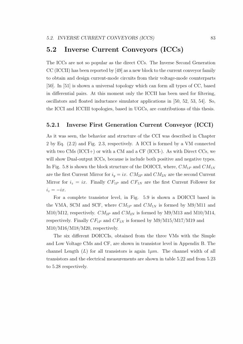
5.2. INVERSE CURRENT CONVEYORS (ICCS) 83
5.2 Inverse Current Conveyors (ICCs)
The ICCs are not so popular as the direct CCs. The Inverse Second Generation
CC (ICCII) has been reported by [49] as a new block to the current conveyor family
to obtain and design current-mode circuits from their voltage-mode counterparts
[50]. In [51] is shown a universal topology which can form all types of CC, based
in differential pairs. At this moment only the ICCII has been used for filtering,
oscillators and floated inductance simulator applications in [50, 52, 53, 54]. So,
the ICCI and ICCIII topologies, based in UGCs, are contributions of this thesis.
5.2.1 Inverse First Generation Current Conveyor (ICCI)
As it was seen, the behavior and structure of the CCI was described in Chapter
2 by Eq. (2.2) and Fig. 2.3, respectively. A ICCI is formed by a VM connected
with two CMs (ICCI+) or with a CM and a CF (ICCI-). As with Direct CCs, we
will show Dual-output ICCs, because is include both positive and negative types.
In Fig. 5.8 is shown the block structure of the DOICCI, where, CM1P and CM1N
are the first Current Mirror for iy = ix. CM2P and CM2N are the second Current
Mirror for iz = ix. Finally CF1P and CF1N are the first Current Follower for
iz = −ix.
For a complete transistor level, in Fig. 5.9 is shown a DOICCI based in
the VMA, SCM and SCF, where CM1P and CM1N is formed by M9/M11 and
M10/M12, respectively. CM2P and CM2N is formed by M9/M13 and M10/M14,
respectively. Finally CF1P and CF1N is formed by M9/M15/M17/M19 and
M10/M16/M18/M20, respectively.
The six different DOICCIs, obtained from the three VMs with the Simple
and Low Voltage CMs and CF, are shown in transistor level in Appendix B. The
channel Length (L) for all transistors is again 1µm. The channel width of all
transistors and the electrical measurements are shown in table 5.22 and from 5.23
to 5.28 respectively.

84 CHAPTER 5. DIRECT AND INVERSE CURRENT CONVEYORS
Figure 5.8: DOICCI structure.
Figure 5.9: DOICCI-VMA-S
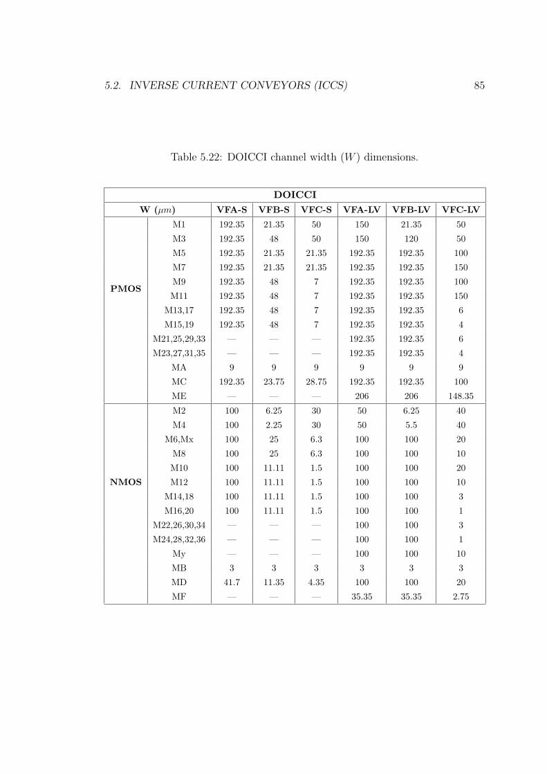
5.2. INVERSE CURRENT CONVEYORS (ICCS) 85
Table 5.22: DOICCI channel width (W ) dimensions.
DOICCIW (µm) VFA-S VFB-S VFC-S VFA-LV VFB-LV VFC-LV
PMOS
M1 192.35 21.35 50 150 21.35 50
M3 192.35 48 50 150 120 50
M5 192.35 21.35 21.35 192.35 192.35 100
M7 192.35 21.35 21.35 192.35 192.35 150
M9 192.35 48 7 192.35 192.35 100
M11 192.35 48 7 192.35 192.35 150
M13,17 192.35 48 7 192.35 192.35 6
M15,19 192.35 48 7 192.35 192.35 4
M21,25,29,33 — — — 192.35 192.35 6
M23,27,31,35 — — — 192.35 192.35 4
MA 9 9 9 9 9 9
MC 192.35 23.75 28.75 192.35 192.35 100
ME — — — 206 206 148.35
NMOS
M2 100 6.25 30 50 6.25 40
M4 100 2.25 30 50 5.5 40
M6,Mx 100 25 6.3 100 100 20
M8 100 25 6.3 100 100 10
M10 100 11.11 1.5 100 100 20
M12 100 11.11 1.5 100 100 10
M14,18 100 11.11 1.5 100 100 3
M16,20 100 11.11 1.5 100 100 1
M22,26,30,34 — — — 100 100 3
M24,28,32,36 — — — 100 100 1
My — — — 100 100 10
MB 3 3 3 3 3 3
MD 41.7 11.35 4.35 100 100 20
MF — — — 35.35 35.35 2.75
86 CHAPTER 5. DIRECT AND INVERSE CURRENT CONVEYORS
Table 5.23: DOICCI-VMA-S electrical parameter measurements
DOICCI-VMA-S
Term. Resistance Ry = 239.8KΩ Rx = 34.41Ω Rz+ = 240.14KΩ Rz− = 227.65KΩ
Analysis V(x/y) I(y/x) I(z+/x) I(z−/x)
DCvVoffset (µV ) -75.68 — — —
VT.C. (mV ) ±400 — — —
DCiIOffset (nA) — 131.31 131.31 -728.54
IT.C. (mA) — ±8 ±8 ±6
ACv
Gain (V/V ) -0.957 — — —
BWv (MHz) 17.7 — — —
Onoise (V/(Hz)1/2) 12.93µ — — —
Inoise (V/(Hz)1/2) 13.5µ — — —
ACi
Gain (A/A) — 1.028 1.028 -1.082
BWi (MHz) — 50.4 50.4 41.9
Onoise (V/(Hz)1/2) — 7.030n 7.030n 7.030n
Inoise (V/(Hz)1/2) — 7.037n 7.037n 7.023n
Tranv
SR (V/µseg) -22.62 — — —
ST (nseg) 30.6 — — —
THD (%) 3.75 — — —
SNR (dB) -78.0 — — —
Trani
SR (A/seg) — 9154.2 9156.9 -8354.1
ST (nseg) — 15 15 21.1
THD (m%) — 84.82 48.19 98.5
SNR (dB) — -35.2 -39.4 -42.3
Table 5.24: DOICCI-VMB-S electrical parameter measurements
DOICCI-VMB-S
Term. Resistance Ry = 478.02KΩ Rx = 83.25Ω Rz+ = 472.53KΩ Rz− = 457.00KΩ
Cc 1pF
Analysis V(x/y) I(y/x) I(z+/x) I(z−/x)
DCvVoffset (µV ) -752.96 — — —
VT.C. (mV ) ±400 — — —
DCiIOffset (nA) — 394.03 394.03 -576.69
IT.C. (mA) — ±0.90 ±0.90 ±0.90
ACv
Gain (V/V ) -0.986 — — —
BWv (MHz) 57.7 — — —
Onoise (V/(Hz)1/2) 13.26µ — — —
Inoise (V/(Hz)1/2) 13.45µ — — —
ACi
Gain (A/A) — 1.015 1.015 -1.047
BWi (MHz) — 121 121 90.0
Onoise (V/(Hz)1/2) — 7.030n 7.030n 7.030n
Inoise (V/(Hz)1/2) — 7.037n 7.037n 7.023n
Tranv
SR (V/µseg) -74.02 — — —
ST (nseg) 32.4 — — —
THD (%) 4.49 — — —
SNR (dB) -104 — — —
Trani
SR (A/seg) — 13569 13590 -11872
ST (nseg) — 11.7 11.7 25.6
THD (m%) — 213.48 213.56 453.1
SNR (dB) — -63.9 -61.1 -60.3

5.2. INVERSE CURRENT CONVEYORS (ICCS) 87
Table 5.25: DOICCI-VMC-S electrical parameter measurements
DOICCI-VMC-S
Term. Resistance Ry = 157.68KΩ Rx = 116.61Ω Rz+ = 704.36KΩ Rz− = 697.97KΩ
Cc 2pF
Analysis V(x/y) I(y/x) I(z+/x) I(z−/x)
DCvVoffset (µV ) -184.42 — — —
VT.C. (mV) ±400 — — —
DCiIOffset (nA) — 615.69 615.69 -661.91
IT.C. (mA) — ±0.05 ±0.05 ±0.05
ACv
Gain (V/V ) -0.985 — — —
BWv (MHz) 27.1 — — —
Onoise (V/(Hz)1/2) 14.66µ — — —
Inoise (V/(Hz)1/2) 14.88µ — — —
ACi
Gain (A/A) — 1.011 1.011 -1.018
BWi (MHz) — 81.5 81.5 87.1
Onoise (V/(Hz)1/2) — 7.030n 7.030n 7.030n
Inoise (V/(Hz)1/2) — 7.037n 7.037n 7.023n
Tranv
SR (V/µseg) -30.15 — — —
ST (nseg) 52.7 — — —
THD (%) 4.48 — — —
SNR (dB) -104 — — —
Trani
SR (A/seg) — 11710 11724 -10622
ST (nseg) — 76.5 80.5 76.3
THD (%) — 1.19 1.19 1.26
SNR (dB) — -47.8 -47.8 -48.0
Table 5.26: DOICCI-VMA-LV electrical parameter measurements
DOICCI-VMA-LV
Term. Resistance Ry = 11.08MΩ Rx = 18.61Ω Rz+ = 11.60MΩ Rz− = 11.59MΩ
Vref ±0.5V
Analysis (V ref = ±0.5V ) V(x/y) I(y/x) I(z+/x) I(z−/x)
DCvVoffset (µV ) 442.16 — — —
VT.C. (mV ) ±300 — — —
DCiIOffset (nA) — 56.46 56.46 -55.40
IT.C. (mA) — ±0.3 ±0.3 ±0.3
ACv
Gain (V/V ) -0.994 — — —
BWv (MHz) 19.8 — — —
Onoise (V/(Hz)1/2) 13.37µ — — —
Inoise (V/(Hz)1/2) 13.44µ — — —
ACi
Gain (A/A) — 1.002 1.002 -1.007
BWi (MHz) — 54.3 54.3 57.9
Onoise (V/(Hz)1/2) — 7.030n 7.030n 7.030n
Inoise (V/(Hz)1/2) — 7.037n 7.037n 7.023n
Tranv
SR (V/µseg) -15.75 — — —
ST (nseg) 43 — — —
THD (%) 3.2 — — —
SNR (dB) -75.2 — — —
Trani
SR (A/seg) — 8396.4 8407.2 -7989.7
ST (nseg) — 12.5 12.5 21.3
THD (m%) — 137.86 129.95 153.62
SNR (dB) — -75.0 -76.3 -73.6

88 CHAPTER 5. DIRECT AND INVERSE CURRENT CONVEYORS
Table 5.27: DOICCI-VMB-LV electrical parameter measurements
DOICCI-VMB-LV
Term. Resistance Ry = 12.85MΩ Rx = 23.57Ω Rz+ = 11.99MΩ Rz− = 11.98MΩ
Cc 1pF
Vref ±0.4V
Analysis V(x/y) I(y/x) I(z+/x) I(z−/x)
DCvVoffset (µV ) -190.75 — — —
VT.C. (mV ) ±400 — — —
DCiIOffset (nA) — 43.75 43.75 -47.92
IT.C. (mA) — ±0.5 ±0.5 ±0.5
ACv
Gain (V/V ) -0.997 — — —
BWv (MHz) 45.7 — — —
Onoise (V/(Hz)1/2) 12.4µ — — —
Inoise (V/(Hz)1/2) 12.4µ — — —
ACi
Gain (A/A) — 1.0007 1.0007 -1.003
BWi (MHz) — 88.4 88.4 85.7
Onoise (V/(Hz)1/2) — 7.030n 7.030n 7.030n
Inoise (V/(Hz)1/2) — 7.037n 7.037n 7.023n
Tranv
SR (V/µseg) -40.25 — — —
ST (nseg) 54.3 — — —
THD (%) 5.01 — — —
SNR (dB) -84.3 — — —
Trani
SR (A/seg) — 11129 11128 -10021
ST (nseg) — 22.3 22.5 19.4
THD (m%) — 81.69 80.63 128.67
SNR (dB) — -60.5 -73.6 -71.7
Table 5.28: DOICCI-VMC-LV electrical parameter measurements
DOICCI-VMC-LV
Term. Resistance Ry = 5.01MΩ Rx = 76.6Ω Rz+ = 23.93MΩ Rz− = 23.86MΩ
Cc 2pF
Vref ±0.4V
Analysis V(x/y) I(y/x) I(z+/x) I(z−/x)
DCvVoffset (µV ) -169.68 — — —
VT.C. (mV ) ±400 — — —
DCiIOffset (nA) — 13.53 13.54 -10.06
IT.C. (mA) — ±0.05 ±0.05 ±0.05
ACv
Gain (V/V ) -0.998 — — —
BWv (MHz) 25.4 — — —
Onoise (V/(Hz)1/2) 13.22µ — — —
Inoise (V/(Hz)1/2) 13.22µ — — —
ACi
Gain (A/A) — 1.0007 1.0007 -1.0016
BWi (MHz) — 71.0 71.0 70.6
Onoise (V/(Hz)1/2) — 7.030n 7.030n 7.030n
Inoise (V/(Hz)1/2) — 7.037n 7.037n 7.023n
Tranv
SR (V/µseg) -28.73 — — —
ST (nseg) 54 — — —
THD (%) 5.03 — — —
SNR (dB) -82.9 — — —
Trani
SR (A/seg) — 7712.7 7701.8 -7458
ST (nseg) — 128 132.5 127.7
THD (m%) — 413.13 410.75 461.43
SNR (dB) — -55.8 -55.5 -55.0
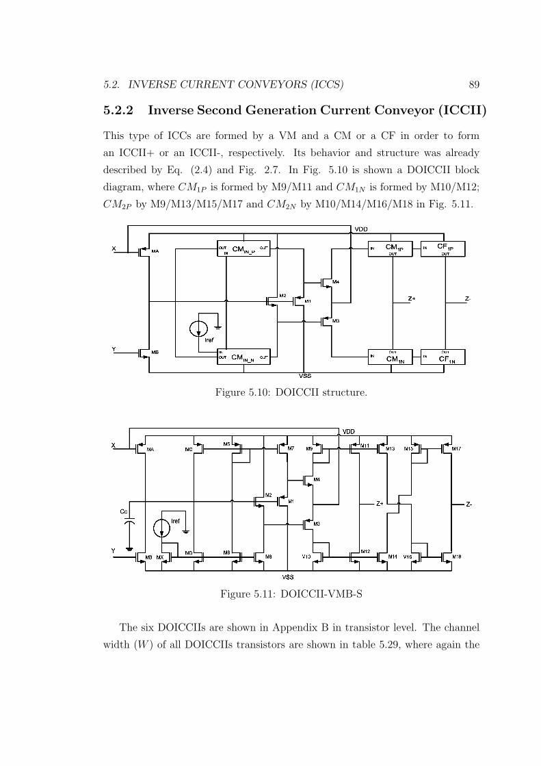
5.2. INVERSE CURRENT CONVEYORS (ICCS) 89
5.2.2 Inverse Second Generation Current Conveyor (ICCII)
This type of ICCs are formed by a VM and a CM or a CF in order to form
an ICCII+ or an ICCII-, respectively. Its behavior and structure was already
described by Eq. (2.4) and Fig. 2.7. In Fig. 5.10 is shown a DOICCII block
diagram, where CM1P is formed by M9/M11 and CM1N is formed by M10/M12;
CM2P by M9/M13/M15/M17 and CM2N by M10/M14/M16/M18 in Fig. 5.11.
Figure 5.10: DOICCII structure.
Figure 5.11: DOICCII-VMB-S
The six DOICCIIs are shown in Appendix B in transistor level. The channel
width (W ) of all DOICCIIs transistors are shown in table 5.29, where again the
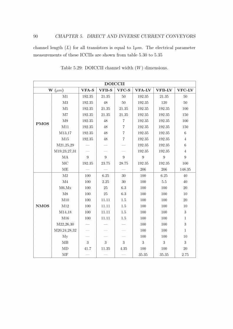
90 CHAPTER 5. DIRECT AND INVERSE CURRENT CONVEYORS
channel length (L) for all transistors is equal to 1µm. The electrical parameter
measurements of these ICCIIs are shown from table 5.30 to 5.35
Table 5.29: DOICCII channel width (W ) dimensions.
DOICCIIW (µm) VFA-S VFB-S VFC-S VFA-LV VFB-LV VFC-LV
PMOS
M1 192.35 21.35 50 192.35 21.35 50
M3 192.35 48 50 192.35 120 50
M5 192.35 21.35 21.35 192.35 192.35 100
M7 192.35 21.35 21.35 192.35 192.35 150
M9 192.35 48 7 192.35 192.35 100
M11 192.35 48 7 192.35 192.35 150
M13,17 192.35 48 7 192.35 192.35 6
M15 192.35 48 7 192.35 192.35 4
M21,25,29 — — — 192.35 192.35 6
M19,23,27,31 — — — 192.35 192.35 4
MA 9 9 9 9 9 9
MC 192.35 23.75 28.75 192.35 192.35 100
ME — — — 206 206 148.35
NMOS
M2 100 6.25 30 100 6.25 40
M4 100 2.25 30 100 5.5 40
M6,Mx 100 25 6.3 100 100 20
M8 100 25 6.3 100 100 10
M10 100 11.11 1.5 100 100 20
M12 100 11.11 1.5 100 100 10
M14,18 100 11.11 1.5 100 100 3
M16 100 11.11 1.5 100 100 1
M22,26,30 — — — 100 100 3
M20,24,28,32 — — — 100 100 1
My — — — 100 100 10
MB 3 3 3 3 3 3
MD 41.7 11.35 4.35 100 100 20
MF — — — 35.35 35.35 2.75
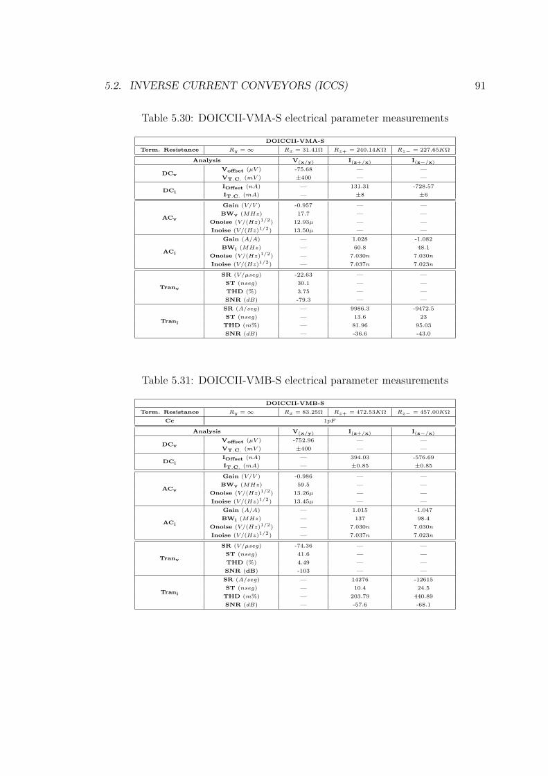
5.2. INVERSE CURRENT CONVEYORS (ICCS) 91
Table 5.30: DOICCII-VMA-S electrical parameter measurements
DOICCII-VMA-S
Term. Resistance Ry = ∞ Rx = 31.41Ω Rz+ = 240.14KΩ Rz− = 227.65KΩ
Analysis V(x/y) I(z+/x) I(z−/x)
DCvVoffset (µV ) -75.68 — —
VT.C. (mV ) ±400 — —
DCiIOffset (nA) — 131.31 -728.57
IT.C. (mA) — ±8 ±6
ACv
Gain (V/V ) -0.957 — —
BWv (MHz) 17.7 — —
Onoise (V/(Hz)1/2) 12.93µ — —
Inoise (V/(Hz)1/2) 13.50µ — —
ACi
Gain (A/A) — 1.028 -1.082
BWi (MHz) — 60.8 48.1
Onoise (V/(Hz)1/2) — 7.030n 7.030n
Inoise (V/(Hz)1/2) — 7.037n 7.023n
Tranv
SR (V/µseg) -22.63 — —
ST (nseg) 30.1 — —
THD (%) 3.75 — —
SNR (dB) -79.3 — —
Trani
SR (A/seg) — 9986.3 -9472.5
ST (nseg) — 13.6 23
THD (m%) — 81.96 95.03
SNR (dB) — -36.6 -43.0
Table 5.31: DOICCII-VMB-S electrical parameter measurements
DOICCII-VMB-S
Term. Resistance Ry = ∞ Rx = 83.25Ω Rz+ = 472.53KΩ Rz− = 457.00KΩ
Cc 1pF
Analysis V(x/y) I(z+/x) I(z−/x)
DCvVoffset (µV ) -752.96 — —
VT.C. (mV ) ±400 — —
DCiIOffset (nA) — 394.03 -576.69
IT.C. (mA) — ±0.85 ±0.85
ACv
Gain (V/V ) -0.986 — —
BWv (MHz) 59.5 — —
Onoise (V/(Hz)1/2) 13.26µ — —
Inoise (V/(Hz)1/2) 13.45µ — —
ACi
Gain (A/A) — 1.015 -1.047
BWi (MHz) — 137 98.4
Onoise (V/(Hz)1/2) — 7.030n 7.030n
Inoise (V/(Hz)1/2) — 7.037n 7.023n
Tranv
SR (V/µseg) -74.36 — —
ST (nseg) 41.6 — —
THD (%) 4.49 — —
SNR (dB) -103 — —
Trani
SR (A/seg) — 14276 -12615
ST (nseg) — 10.4 24.5
THD (m%) — 203.79 440.89
SNR (dB) — -57.6 -68.1
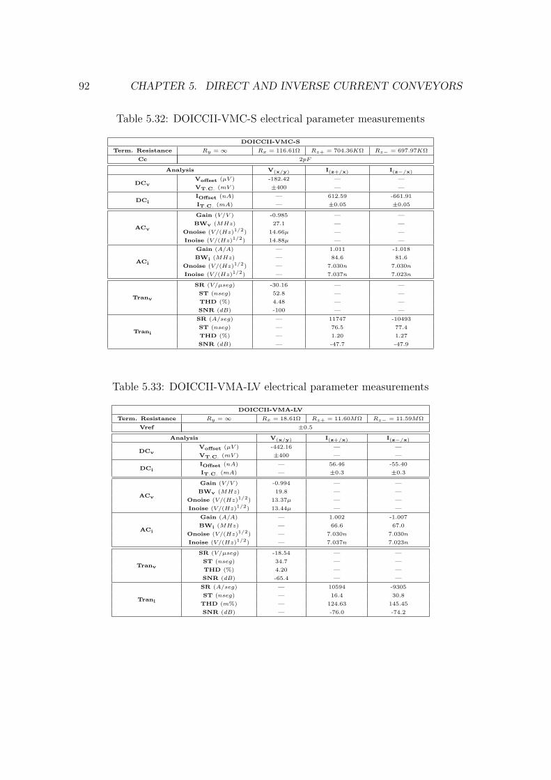
92 CHAPTER 5. DIRECT AND INVERSE CURRENT CONVEYORS
Table 5.32: DOICCII-VMC-S electrical parameter measurements
DOICCII-VMC-S
Term. Resistance Ry = ∞ Rx = 116.61Ω Rz+ = 704.36KΩ Rz− = 697.97KΩ
Cc 2pF
Analysis V(x/y) I(z+/x) I(z−/x)
DCvVoffset (µV ) -182.42 — —
VT.C. (mV ) ±400 — —
DCiIOffset (nA) — 612.59 -661.91
IT.C. (mA) — ±0.05 ±0.05
ACv
Gain (V/V ) -0.985 — —
BWv (MHz) 27.1 — —
Onoise (V/(Hz)1/2) 14.66µ — —
Inoise (V/(Hz)1/2) 14.88µ — —
ACi
Gain (A/A) — 1.011 -1.018
BWi (MHz) — 84.6 81.6
Onoise (V/(Hz)1/2) — 7.030n 7.030n
Inoise (V/(Hz)1/2) — 7.037n 7.023n
Tranv
SR (V/µseg) -30.16 — —
ST (nseg) 52.8 — —
THD (%) 4.48 — —
SNR (dB) -100 — —
Trani
SR (A/seg) — 11747 -10493
ST (nseg) — 76.5 77.4
THD (%) — 1.20 1.27
SNR (dB) — -47.7 -47.9
Table 5.33: DOICCII-VMA-LV electrical parameter measurements
DOICCII-VMA-LV
Term. Resistance Ry = ∞ Rx = 18.61Ω Rz+ = 11.60MΩ Rz− = 11.59MΩ
Vref ±0.5
Analysis V(x/y) I(z+/x) I(z−/x)
DCvVoffset (µV ) -442.16 — —
VT.C. (mV ) ±400 — —
DCiIOffset (nA) — 56.46 -55.40
IT.C. (mA) — ±0.3 ±0.3
ACv
Gain (V/V ) -0.994 — —
BWv (MHz) 19.8 — —
Onoise (V/(Hz)1/2) 13.37µ — —
Inoise (V/(Hz)1/2) 13.44µ — —
ACi
Gain (A/A) — 1.002 -1.007
BWi (MHz) — 66.6 67.0
Onoise (V/(Hz)1/2) — 7.030n 7.030n
Inoise (V/(Hz)1/2) — 7.037n 7.023n
Tranv
SR (V/µseg) -18.54 — —
ST (nseg) 34.7 — —
THD (%) 4.20 — —
SNR (dB) -65.4 — —
Trani
SR (A/seg) — 10594 -9305
ST (nseg) — 16.4 30.8
THD (m%) — 124.63 145.45
SNR (dB) — -76.0 -74.2
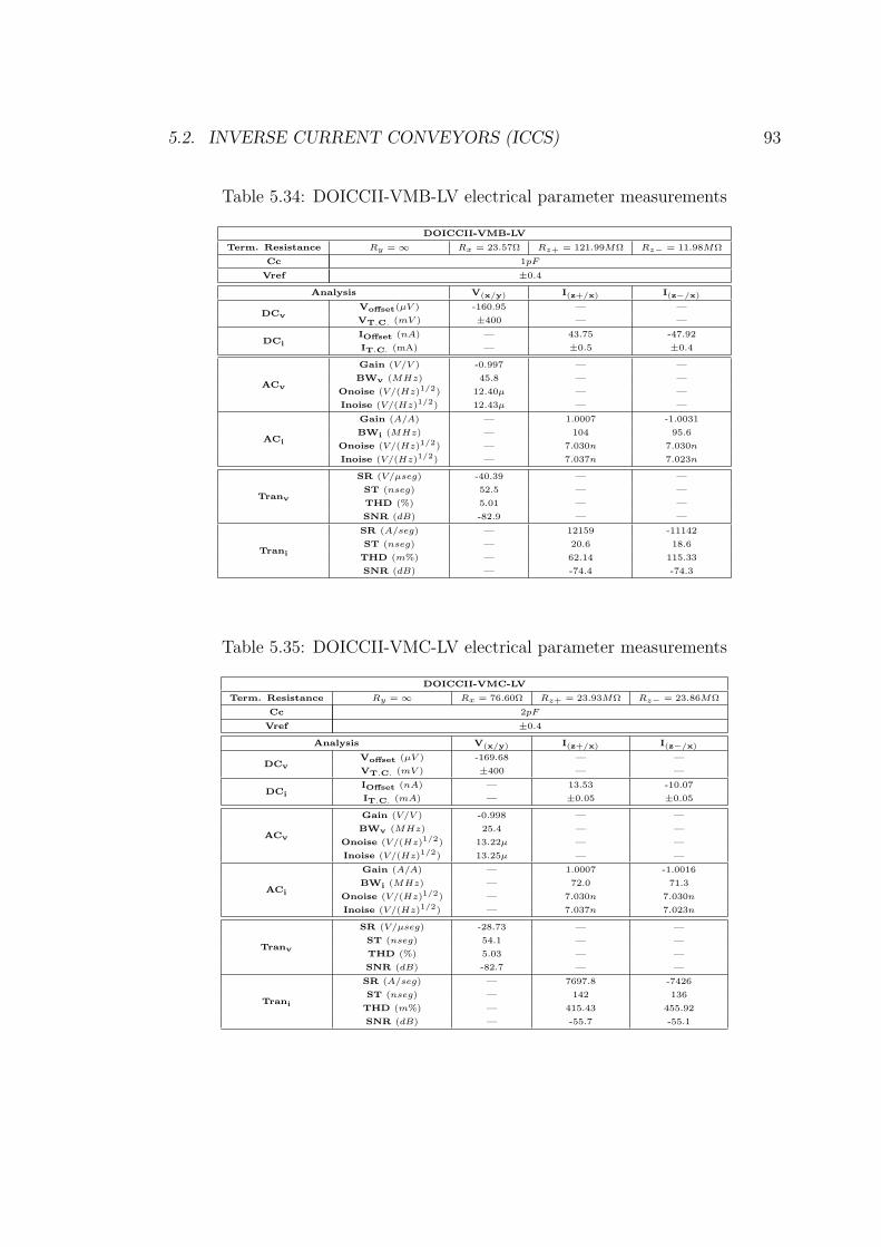
5.2. INVERSE CURRENT CONVEYORS (ICCS) 93
Table 5.34: DOICCII-VMB-LV electrical parameter measurements
DOICCII-VMB-LV
Term. Resistance Ry = ∞ Rx = 23.57Ω Rz+ = 121.99MΩ Rz− = 11.98MΩ
Cc 1pF
Vref ±0.4
Analysis V(x/y) I(z+/x) I(z−/x)
DCvVoffset(µV ) -160.95 — —
VT.C. (mV ) ±400 — —
DCiIOffset (nA) — 43.75 -47.92
IT.C. (mA) — ±0.5 ±0.4
ACv
Gain (V/V ) -0.997 — —
BWv (MHz) 45.8 — —
Onoise (V/(Hz)1/2) 12.40µ — —
Inoise (V/(Hz)1/2) 12.43µ — —
ACi
Gain (A/A) — 1.0007 -1.0031
BWi (MHz) — 104 95.6
Onoise (V/(Hz)1/2) — 7.030n 7.030n
Inoise (V/(Hz)1/2) — 7.037n 7.023n
Tranv
SR (V/µseg) -40.39 — —
ST (nseg) 52.5 — —
THD (%) 5.01 — —
SNR (dB) -82.9 — —
Trani
SR (A/seg) — 12159 -11142
ST (nseg) — 20.6 18.6
THD (m%) — 62.14 115.33
SNR (dB) — -74.4 -74.3
Table 5.35: DOICCII-VMC-LV electrical parameter measurements
DOICCII-VMC-LV
Term. Resistance Ry = ∞ Rx = 76.60Ω Rz+ = 23.93MΩ Rz− = 23.86MΩ
Cc 2pF
Vref ±0.4
Analysis V(x/y) I(z+/x) I(z−/x)
DCvVoffset (µV ) -169.68 — —
VT.C. (mV ) ±400 — —
DCiIOffset (nA) — 13.53 -10.07
IT.C. (mA) — ±0.05 ±0.05
ACv
Gain (V/V ) -0.998 — —
BWv (MHz) 25.4 — —
Onoise (V/(Hz)1/2) 13.22µ — —
Inoise (V/(Hz)1/2) 13.25µ — —
ACi
Gain (A/A) — 1.0007 -1.0016
BWi (MHz) — 72.0 71.3
Onoise (V/(Hz)1/2) — 7.030n 7.030n
Inoise (V/(Hz)1/2) — 7.037n 7.023n
Tranv
SR (V/µseg) -28.73 — —
ST (nseg) 54.1 — —
THD (%) 5.03 — —
SNR (dB) -82.7 — —
Trani
SR (A/seg) — 7697.8 -7426
ST (nseg) — 142 136
THD (m%) — 415.43 455.92
SNR (dB) — -55.7 -55.1
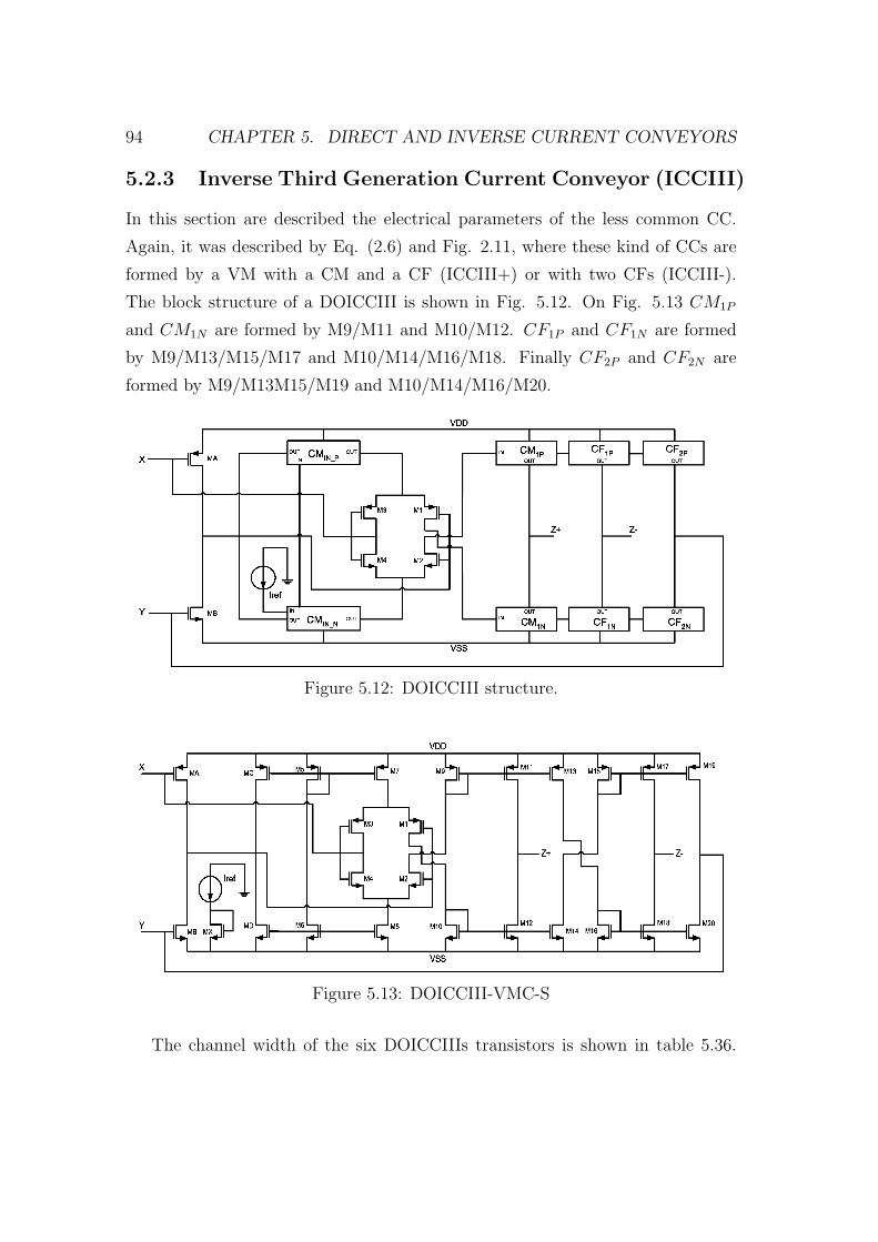
94 CHAPTER 5. DIRECT AND INVERSE CURRENT CONVEYORS
5.2.3 Inverse Third Generation Current Conveyor (ICCIII)
In this section are described the electrical parameters of the less common CC.
Again, it was described by Eq. (2.6) and Fig. 2.11, where these kind of CCs are
formed by a VM with a CM and a CF (ICCIII+) or with two CFs (ICCIII-).
The block structure of a DOICCIII is shown in Fig. 5.12. On Fig. 5.13 CM1P
and CM1N are formed by M9/M11 and M10/M12. CF1P and CF1N are formed
by M9/M13/M15/M17 and M10/M14/M16/M18. Finally CF2P and CF2N are
formed by M9/M13M15/M19 and M10/M14/M16/M20.
Figure 5.12: DOICCIII structure.
Figure 5.13: DOICCIII-VMC-S
The channel width of the six DOICCIIIs transistors is shown in table 5.36.

5.2. INVERSE CURRENT CONVEYORS (ICCS) 95
The electrical measurements shown from table 5.37 to 5.42. The channel width
(W ) for all transistors is equal to 1 µm.
Table 5.36: DOICCIII channel width (W ) dimensions.
DOICCIIIW (µm) VFA-S VFB-S VFC-S VFA-LV VFB-LV VFC-LV
PMOS
M1 192.35 21.35 50 192.35 21.35 50
M3 192.35 48 50 192.35 120 50
M5 192.35 21.35 21.35 192.35 192.35 100
M7 192.35 21.35 21.35 192.35 192.35 150
M9 192.35 48 7 192.35 192.35 100
M11 192.35 48 7 192.35 192.35 150
M13,17 192.35 48 7 192.35 192.35 6
M15,19 192.35 48 7 192.35 192.35 4
M21,25,29,33 — — — 192.35 192.35 6
M23,27,31,35 — — — 192.35 192.35 4
MA 9 9 9 9 9 9
MC 192.35 23.75 28.75 192.35 192.35 100
ME — — — 206 206 148.35
NMOS
M2 100 6.25 30 100 6.25 40
M4 100 2.25 30 100 5.5 40
M6,Mx 100 25 6.3 100 100 20
M8 100 25 6.3 100 100 10
M10 100 11.11 1.5 100 100 20
M12 100 11.11 1.5 100 100 10
M14,18 100 11.11 1.5 100 100 3
M16,20 100 11.11 1.5 100 100 1
M22,26,30,34 — — — 100 100 3
M24,28,32,36 — — — 100 100 1
My — — — 100 100 10
MB 3 3 3 3 3 3
MD 41.7 11.35 4.35 100 100 20
MF — — — 35.35 35.35 2.75
96 CHAPTER 5. DIRECT AND INVERSE CURRENT CONVEYORS
Table 5.37: DOICCIII-VMA-S electrical parameter measurements
DOICCIII-VMA-S
Term. Resistance Ry = 228.49KΩ Rx = 34.41Ω Rz+ = 240.14KΩ Rz− = 227.65KΩ
Analysis V(x/y) I(y/x) I(z+/x) I(z−/x)
DCvVoffset (µV ) -75.68 — — —
VT.C. (mV ) ±400 — — —
DCiIOffset (nA) — -728.54 131.31 -728.54
IT.C. (mA) — ±6 ±8 ±6
ACv
Gain (V/V ) -0.957 — — —
BWv (MHz) 17.7 — — —
Onoise (V/(Hz)1/2) 12.93µ — — —
Inoise (V/(Hz)1/2) 13.50µ — — —
ACi
Gain (A/A) — -1.0821 1.0286 -1.0821
BWi (MHz) — 43.1 60.9 43.1
Onoise (V/(Hz)1/2) — 7.030n 7.030n 7.030n
Inoise (V/(Hz)1/2) — 7.023n 7.037n 7.023n
Tranv
SR (V/µseg) -22.63 — — —
ST (nseg) 29.6 — — —
THD (%) 3.75 — — —
SNR (dB) -78.3 — — —
Trani
SR (A/seg) — -8454.2 9991.1 -8458.2
ST (nseg) — 20 13.2 20.1
THD (m%) — 97.45 61.81 97.4
SNR (dB) — -42.2 -35.6 -42.2
Table 5.38: DOICCIII-VMB-S electrical parameter measurements
DOICCIII-VMB-S
Term. Resistance Ry = 450.32KΩ Rx = 83.25Ω Rz+ = 472.53KΩ Rz− = 457.00KΩ
Cc 1pF
Analysis V(x/y) I(y/x) I(z+/x) I(z−/x)
DCvVoffset (µV ) -752.96 — — —
VT.C. (mV ) ±400 — — —
DCiIOffset (nA) — -576.69 394.03 -576.69
IT.C. (mA) — ±0.80 ±0.85 ±0.80
ACv
Gain (V/V ) -0.986 — — —
BWv (MHz) 57.8 — — —
Onoise (V/(Hz)1/2) 13.26µ — — —
Inoise (V/(Hz)1/2) 13.45µ — — —
ACi
Gain (A/A) — -1.047 1.015 -1.047
BWi (MHz) — 84.2 137 84.2
Onoise (V/(Hz)1/2) — 7.030n 7.030n 7.030n
Inoise (V/(Hz)1/2) — 7.023n 7.037n 7.023n
Tranv
SR (V/µseg) -74.36 — — —
ST (nseg) 39.7 — — —
THD (%) 4.49 — — —
SNR (dB) -102 — — —
Trani
SR (A/seg) — -12272 14282 -12244
ST (nseg) — 34.9 10.9 35
THD (m%) — 456.84 204.59 456.76
SNR (dB) — -70.7 -65.7 -74.1

5.2. INVERSE CURRENT CONVEYORS (ICCS) 97
Table 5.39: DOICCIII-VMC-S electrical parameter measurements
DOICCIII-VMC-S
Term. Resistance Ry = 283.49KΩ Rx = 116.61Ω Rz+ = 704.36KΩ Rz− = 697.97KΩ
Cc 2pF
Analysis V(x/y) I(y/x) I(z+/x) I(z−/x)
DCvVoffset (µV ) -184.42 — — —
VT.C. (mV ) ±430 — — —
DCiIOffset (nA) — -661.91 615.59 -661.91
IT.C. (mA) — ±0.05 ±0.05 ±0.05
ACv
Gain (V/V ) -0.985 — — —
BWv (MHz) 27.2 — — —
Onoise (V/(Hz)1/2) 14.66µ — — —
Inoise (V/(Hz)1/2) 14.88µ — — —
ACi
Gain (A/A) — -1.018 1.011 -1.018
BWi (MHz) — 79.7 84.7 79.7
Onoise (V/(Hz)1/2) — 7.030n 7.030n 7.030n
Inoise (V/(Hz)1/2) — 7.023n 7.037n 7.023n
Tranv
SR (V/µseg) -30.16 — — —
ST (nseg) 52.5 — — —
THD (%) 4.48 — — —
SNR (dB) -102 — — —
Trani
SR (A/seg) — -10557 11744 -10575
ST (nseg) — 78.9 77.8 78.3
THD (%) — 1.27 1.19 1.23
SNR (dB) — -47.9 -47.8 -48.3
Table 5.40: DOICCIII-VMA-LV electrical parameter measurements
DOICCIII-VMA-LV
Term. Resistance Ry = 12.14MΩ Rx = 18.61Ω Rz+ = 11.61MΩ Rz− = 11.60MΩ
Vref ±0.5V
Analysis V(x/y) I(y/x) I(z+/x) I(z−/x)
DCvVoffset (µV ) -493.34 — — —
VT.C. (mV ) ±400 — — —
DCiIOffset (nA) — -55.36 56.41 -55.36
IT.C. (mA) — ±0.3 ±0.3 ±0.3
ACv
Gain (V/V ) -0.994 — — —
BWv (MHz) 19.9 — — —
Onoise (V/(Hz)1/2) 13.37µ — — —
Inoise (V/(Hz)1/2) 13.44µ — — —
ACi
Gain (A/A) — -1.007 1.002 -1.007
BWi (MHz) — 57.7 66.7 57.7
Onoise (V/(Hz)1/2) — 7.030n 7.030n 7.030n
Inoise (V/(Hz)1/2) — 7.023n 7.037n 7.023n
Tranv
SR (V/µseg) -19.14 — — —
ST (nseg) 35.5 — — —
THD (%) 4.48 — — —
SNR (dB) -65.7 — — —
Trani
SR (A/seg) — -8722.4 10186 -8733.1
ST (nseg) — 22.5 17.4 22.4
THD (m%) — 159.46 135.63 162.02
SNR (dB) — -74.5 -76.4 -73.4
98 CHAPTER 5. DIRECT AND INVERSE CURRENT CONVEYORS
Table 5.41: DOICCIII-VMB-LV electrical parameter measurements
DOICCIII-VMB-LV
Term. Resistance Ry = 11.25MΩ Rx = 23.57Ω Rz+ = 11.99MΩ Rz− = 11.98MΩ
Cc 1pF
Vref ±0.4V
Analysis V(x/y) I(y/x) I(z+/x) I(z−/x)
DCvVoffset (µV ) -190.65 — — —
VT.C. (mV ) ±400 — — —
DCiIOffset (nA) — -47.92 43.75 -47.92
IT.C. (mA) — ±0.5 ±0.5 ±0.45
ACv
Gain (V/V ) -0.997 — — —
BWv (MHz) 45.8 — — —
Onoise (V/(Hz)1/2) 12.40µ — — —
Inoise (V/(Hz)1/2) 12.43µ — — —
ACi
Gain (A/A) — -1.003 1.0007 -1.003
BWi (MHz) — 79.8 104 79.8
Onoise (V/(Hz)1/2) — 7.030n 7.030n 7.030n
Inoise (V/(Hz)1/2) — 7.023n 7.037n 7.023n
Tranv
SR (V/µseg) -40.39 — — —
ST (nseg) 54.4 — — —
THD (%) 5.01 — — —
SNR (dB) -83.8 — — —
Trani
SR (A/seg) — -9528.4 12159 -9523.7
ST (nseg) — 25.4 18.4 25.3
THD (m%) — 119.10 58.94 119.61
SNR (dB) — -69.7 -75.1 -72.9
Table 5.42: DOICCIII-VMC-LV electrical parameter measurements
DOICCIII-VMC-LV
Term. Resistance Ry = 8.63MΩ Rx = 76.60Ω Rz+ = 23.93MΩ Rz− = 23.86MΩ
Cc 2pF
Vref ±0.4V
Analysis V(x/y) I(y/x) I(z+/x) I(z−/x)
DCvVoffset (µV ) -169.68 — — —
VT.C. (mV ) ±400 — — —
DCiIOffset (nA) — -10.07 13.53 -10.07
IT.C. (mA) — ±0.05 ±0.05 ±0.05
ACv
Gain (V/V ) -0.998 — — —
BWv (MHz) 25.4 — — —
Onoise (V/(Hz)1/2) 13.22µ — — —
Inoise (V/(Hz)1/2) 13.25µ — — —
ACi
Gain (A/A) — -1.0016 1.0007 -1.0016
BWi (MHz) — 70.3 72.1 70.3
Onoise (V/(Hz)1/2) — 7.030n 7.030n 7.030n
Inoise (V/(Hz)1/2) — 7.023n 7.037n 7.023n
Tranv
SR (V/µseg) -28.73 — — —
ST (nseg) 54 — — —
THD (%) 5.03 — — —
SNR (dB) -83.1 — — —
Trani
SR (A/seg) — -7589.2 7697.7 -7580.1
ST (nseg) — 137.6 133 137.6
THD (m%) — 467.26 416.10 465.93
SNR (dB) — -55.0 -55.7 -55.0

5.3. PARASITIC ELEMENTS 99
5.3 Parasitic Elements
Due to the fact that the CCs are built with CMOS transistors, they present
parasitic components inherent to their topology. These elements influence the
behavior of the CCs at high frequencies, principally the parasitic capacitances
which are responsibles of the limited frequency behavior [30].
In Fig. 5.14 are shown the most important parasitic elements in the CCs,
where (RY //CY ) constitutes the input impedance on Y-terminal, when output
X-terminal is open. RY , RX and RZ are the low frequency output resistance on
Y, X and Z terminals, respectively, as it was seen before. (RZ//CZ) is the output
impedance on Z-terminal, where RZ and CZ can reproduce the high frequency
peak of the output current flowing on Z-terminal when it is grounded [55].
Figure 5.14: CCs parasitics elements.
The parasitic elements can be measured from the impedance curve in each
terminal, connecting a voltage source in the interest terminal and dividing its value
with the current through that terminal. So the resistive elements are measured at
low frequency and the capacitances are deduced from the −3dB cut-off frequency
of the magnitude of the input impedance curve [30, 55]. The capacitive parasitic
elements are determined with the following equations:
CY =1
2πfY RY
(5.1)

100 CHAPTER 5. DIRECT AND INVERSE CURRENT CONVEYORS
CZ+ =1
2πfZ+RZ+
(5.2)
CZ− =1
2πfZ−RZ−(5.3)
where fY , fZ+ and fZ− are the −3dB cut-off frequency of the magnitude of
the impedance curve, described before.
In Table 5.43 are shown the capacitive parasitic elements of four CCs, which
are used then in Chapter 6 in some applications.
Table 5.43: CCs capacitive parasitic elements
ELEMENTS DOCCI-VFA-S DOCCII-VFC-S DOCCII-VFB-LV DOICCII-VMC-LV
CY (fF ) 2470 59.89 2.76 8.3
CZ+ (fF ) 568.0 18.34 530.86 18.52
CZ− (fF ) 566.2 18.27 530.26 18.53
Chapter 6
Applications
The CCs can be employed in a very large number of different applications. For
instance, this chapter shows applications of CCs including universal filters, oscil-
lators and inductance simulation.
6.1 CCI Applications
The tested applications for the CCI are two voltage-mode filters and a sinusoidal
oscillator. For these circuits the DOCCI − V FA − SCM was used, because it
has the best gain value between the DOCCIs designed with simple CMs and CFs.
As it will be seen, this filters and oscillator where designed for a CCI+ topology,
so if a Dual-output type will be used, the modification is just to ground the Z−terminal in order to obtain the original CCI needed for each application.
6.1.1 CCI-Based Filters
Band-pass filter (BPF)
A voltage-mode tunable BPF is shown in Fig. 6.1, which is a modified topology
of the universal filter topology presented in [56].
The transfer function of the BPF is shown in Eq. (6.1), and the center fre-
quency of the filter ω0 is shown in Eq. (6.2). As we can see in (6.1), the parasitic
101

102 CHAPTER 6. APPLICATIONS
Figure 6.1: CCI-based BPF Filter
resistance Rx is a dominant parameter that strongly modifies the frequency re-
sponse of the BPF.
V out =sC1R2Rx
s2 [(C1 + C3)C2Rx2R2] + s [(C1 + C3)Rx2 − (C1 − C2 + C3)RxR2] + (R2 + Rx)(6.1)
ω0 =1
Rx
√R2 + Rx
(C1 + C3)C2R2
(6.2)
In order to simulate this filter, the center frequency was chosen to be 3 MHz,
so that the passive elements are: R2 = 5KΩ, C1 = C2 = C3 = 77.15pF and
Rx = 510.44Ω. This value of Rx is obtained with Iref = 50µA. As a result, the
ideal and real frequency responses of the BPF are shown in Fig. 6.2. The ideal
responses were obtained using MatLab (dashed lines), and the real responses were
obtained using HSPICE (solid lines). For instance in the ideal case, to reach a
center frequency of 1.57 MHz, the bias current Iref was varied to 20µA, that
corresponds to a Rx = 1.02KΩ; as mentioned above, for a center frequency of
3 MHz, Iref was varied to 50µA, that corresponds to a Rx = 510.44Ω; and for
a center frequency of 6 MHz, Iref was varied to 160µA, that corresponds to a
Rx = 246.21Ω. In HSPICE, for a center frequency of 1.57 MHz, Iref was varied
to 22µA; for a center frequency of 3 MHz, Iref was varied to 55µA, and for a
center frequency of 6 MHz, Iref was varied to 185µA.
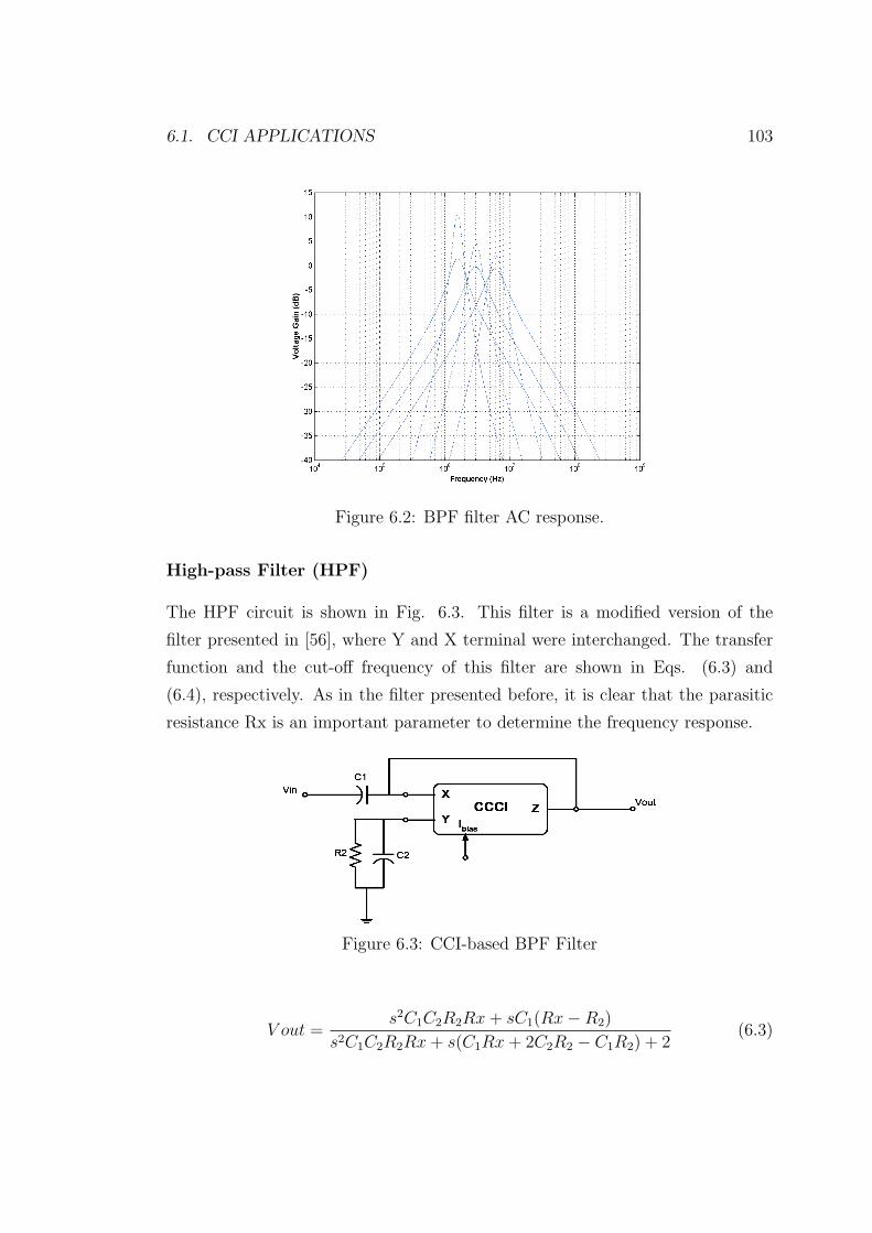
6.1. CCI APPLICATIONS 103
Figure 6.2: BPF filter AC response.
High-pass Filter (HPF)
The HPF circuit is shown in Fig. 6.3. This filter is a modified version of the
filter presented in [56], where Y and X terminal were interchanged. The transfer
function and the cut-off frequency of this filter are shown in Eqs. (6.3) and
(6.4), respectively. As in the filter presented before, it is clear that the parasitic
resistance Rx is an important parameter to determine the frequency response.
Figure 6.3: CCI-based BPF Filter
V out =s2C1C2R2Rx + sC1(Rx−R2)
s2C1C2R2Rx + s(C1Rx + 2C2R2 − C1R2) + 2(6.3)
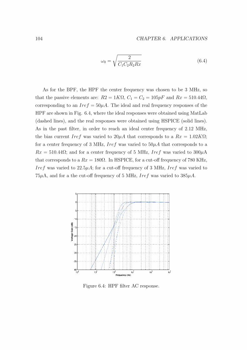
104 CHAPTER 6. APPLICATIONS
ω0 =
√2
C1C2R2Rx(6.4)
As for the BPF, the HPF the center frequency was chosen to be 3 MHz, so
that the passive elements are: R2 = 1KΩ, C1 = C2 = 105pF and Rx = 510.44Ω,
corresponding to an Iref = 50µA. The ideal and real frequency responses of the
HPF are shown in Fig. 6.4, where the ideal responses were obtained using MatLab
(dashed lines), and the real responses were obtained using HSPICE (solid lines).
As in the past filter, in order to reach an ideal center frequency of 2.12 MHz,
the bias current Iref was varied to 20µA that corresponds to a Rx = 1.02KΩ;
for a center frequency of 3 MHz, Iref was varied to 50µA that corresponds to a
Rx = 510.44Ω; and for a center frequency of 5 MHz, Iref was varied to 300µA
that corresponds to a Rx = 180Ω. In HSPICE, for a cut-off frequency of 780 KHz,
Iref was varied to 22.5µA; for a cut-off frequency of 3 MHz, Iref was varied to
75µA, and for a the cut-off frequency of 5 MHz, Iref was varied to 385µA.
Figure 6.4: HPF filter AC response.

6.1. CCI APPLICATIONS 105
6.1.2 Sinusoidal Oscillator
Not only the CCIs can be applied to filtering applications but also they are quite
useful to build an oscillator, as shown in Fig. 6.5 [57]. The characteristic equation
and the oscillation frequency are shown in Eqs. (6.5) and (6.6), respectively. The
oscillation condition is given by Eq. (6.7).
s2
[C1C4
R3 + Rx
]+ s
[C4R3R4 + C2R3(R3 + Rx)
R3R4Rx(R3 + Rx)
]+
1
R4Rx(R3 + Rx)(6.5)
ω0 =
√R3 + Rx
C1C4R4Rx(R3 + Rx)(6.6)
1
C4R3
=1
C2R4
(6.7)
The passive elements values are: C1 > C4, C1 = 40pF , C2 = C4 = 30pF ,
R1 = R4 = 10KΩ. For an ideal case, in order to reach an oscillation frequency of
1.8 MHz, Iref must to be equal to 40µA, and for an oscillation frequency of 3.55
MHz, Iref must to be equal to 350µA. In HSPICE, for an oscillation frequency
of 1.8 MHz, Iref was varied to 70µA, which is shown in Fig. 6.6. And for an
oscillation frequency of 3.5 MHz, Iref was varied to 155µA, shown in Fig. 6.7.
Figure 6.5: CCI-based Sinusoidal Oscillator
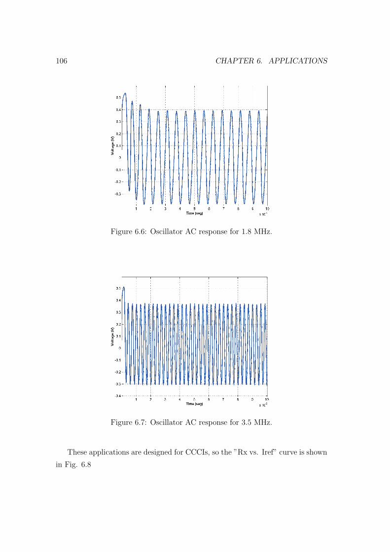
106 CHAPTER 6. APPLICATIONS
Figure 6.6: Oscillator AC response for 1.8 MHz.
Figure 6.7: Oscillator AC response for 3.5 MHz.
These applications are designed for CCCIs, so the ”Rx vs. Iref” curve is shown
in Fig. 6.8
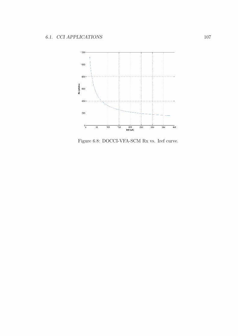
6.1. CCI APPLICATIONS 107
Figure 6.8: DOCCI-VFA-SCM Rx vs. Iref curve.

108 CHAPTER 6. APPLICATIONS
6.2 CCII Applications
The CCII is the most popular configuration, it has been applied to most of the CC
applications. Now it will be shown a universal current-mode filter, two floating
inductance simulators and a FTFN applied to another universal current-mode
filter and to a sinusoidal oscillator.
6.2.1 Universal Current-Mode Filter
This universal filter was already shown ideally in Chapter 3. Now it will be shown
the simulated results. Iref is adjusted to the following values: 27µA for LP, 40µA
for BP, 60µA for HP, and 40µA for Notch. The frequency responses of the CM
universal filter using the DOCCCII−V FC−SCM , as a current controlled type,
are shown in Fig. 6.9.
Figure 6.9: Universal current-mode AC response.
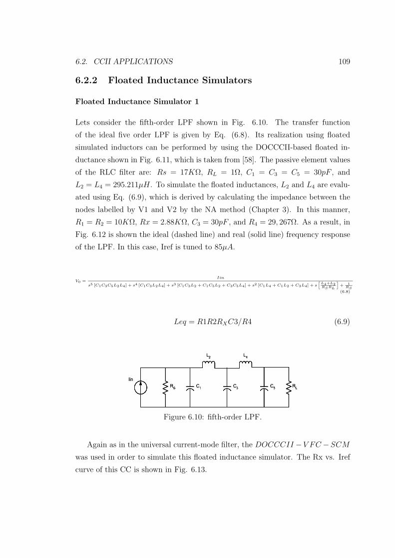
6.2. CCII APPLICATIONS 109
6.2.2 Floated Inductance Simulators
Floated Inductance Simulator 1
Lets consider the fifth-order LPF shown in Fig. 6.10. The transfer function
of the ideal five order LPF is given by Eq. (6.8). Its realization using floated
simulated inductors can be performed by using the DOCCCII-based floated in-
ductance shown in Fig. 6.11, which is taken from [58]. The passive element values
of the RLC filter are: Rs = 17KΩ, RL = 1Ω, C1 = C3 = C5 = 30pF , and
L2 = L4 = 295.211µH. To simulate the floated inductances, L2 and L4 are evalu-
ated using Eq. (6.9), which is derived by calculating the impedance between the
nodes labelled by V1 and V2 by the NA method (Chapter 3). In this manner,
R1 = R2 = 10KΩ, Rx = 2.88KΩ, C3 = 30pF , and R4 = 29, 267Ω. As a result, in
Fig. 6.12 is shown the ideal (dashed line) and real (solid line) frequency response
of the LPF. In this case, Iref is tuned to 85µA.
V0 =Iin
s5 [C1C3C5L2L4] + s4 [C1C3L2L4] + s3 [C1C3L2 + C1C5L2 + C3C5L4] + s2 [C1L4 + C1L2 + C3L4] + sh
L4+L2RSRL
i+ 1
RS(6.8)
Leq = R1R2RXC3/R4 (6.9)
Figure 6.10: fifth-order LPF.
Again as in the universal current-mode filter, the DOCCCII −V FC −SCM
was used in order to simulate this floated inductance simulator. The Rx vs. Iref
curve of this CC is shown in Fig. 6.13.
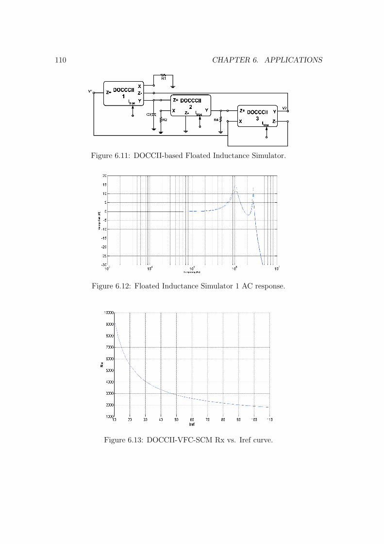
110 CHAPTER 6. APPLICATIONS
Figure 6.11: DOCCII-based Floated Inductance Simulator.
Figure 6.12: Floated Inductance Simulator 1 AC response.
Figure 6.13: DOCCII-VFC-SCM Rx vs. Iref curve.

6.2. CCII APPLICATIONS 111
Floated Inductance Simulator 2
In [59] is shown a DOCCCII-based floated inductor which has the topology shown
in Fig. 6.14. Assuming that Rx1 = Rx2 = Rx3 = Rx, then the symbolic
expression for Leq or the input impedance of the floated inductance simulator
is given by Eq. (6.10). The Cint value can be evaluated using Eq. (6.11).
Figure 6.14: DOCCII-based Floated Inductance Simulator 2.
Leq = 2sCintRx2 (6.10)
Cint =L
2Rx2(6.11)
In Fig. 6.15 is shown the frequency response of the five order LPF. The ideal
response is with a dash line and in a solid line is shown the frequency response
of the filter with the DOCCCII-based inductor equivalent. The passive element
values for the LPF of Fig. 6.10 are: Rs = 17KΩ, RL = 1Ω, C1 = C5 = 10pF ,
C3 = 11pF , L2 = L4 = 295.211µH. Replacing the passive inductors with the
DOCCCII-based floated inductor equivalent, Cint of each DOCCCII has a value
equal to 208.68pF , with a Rx = 841.02Ω, that correspond to an Iref = 50µA.
For this second floated inductance simulator, was used the DOCCII−V FB−LV in order to show that CCs based in low voltage CMs and CFs are suitable too
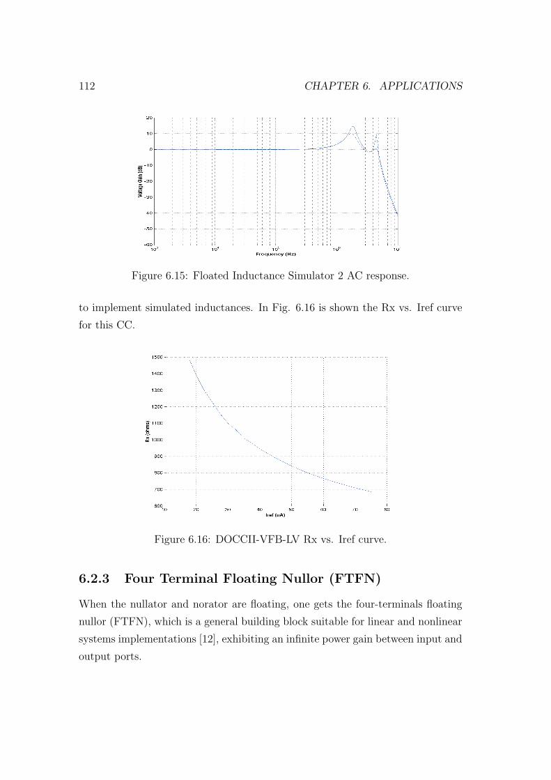
112 CHAPTER 6. APPLICATIONS
Figure 6.15: Floated Inductance Simulator 2 AC response.
to implement simulated inductances. In Fig. 6.16 is shown the Rx vs. Iref curve
for this CC.
Figure 6.16: DOCCII-VFB-LV Rx vs. Iref curve.
6.2.3 Four Terminal Floating Nullor (FTFN)
When the nullator and norator are floating, one gets the four-terminals floating
nullor (FTFN), which is a general building block suitable for linear and nonlinear
systems implementations [12], exhibiting an infinite power gain between input and
output ports.
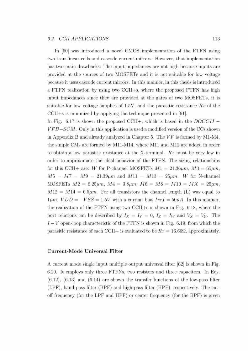
6.2. CCII APPLICATIONS 113
In [60] was introduced a novel CMOS implementation of the FTFN using
two translinear cells and cascode current mirrors. However, that implementation
has two main drawbacks: The input impedances are not high because inputs are
provided at the sources of two MOSFETs and it is not suitable for low voltage
because it uses cascode current mirrors. In this manner, in this thesis is introduced
a FTFN realization by using two CCII+s, where the proposed FTFN has high
input impedances since they are provided at the gates of two MOSFETs, it is
suitable for low voltage supplies of 1.5V, and the parasitic resistance Rx of the
CCII+s is minimized by applying the technique presented in [61].
In Fig. 6.17 is shown the proposed CCII+, which is based in the DOCCII −V FB−SCM . Only in this application is used a modified version of the CCs shown
in Appendix B and already analyzed in Chapter 5. The V F is formed by M1-M4,
the simple CMs are formed by M11-M14, where M11 and M12 are added in order
to obtain a low parasitic resistance at the X-terminal. Rx must be very low in
order to approximate the ideal behavior of the FTFN. The sizing relationships
for this CCII+ are: W for P-channel MOSFETs M1 = 21.36µm, M3 = 65µm,
M5 = M7 = M9 = 21.39µm and M11 = M13 = 25µm. W for N-channel
MOSFETs M2 = 6.25µm, M4 = 3.8µm, M6 = M8 = M10 = MX = 25µm,
M12 = M14 = 6.5µm. For all transistors the channel length (L) was equal to
1µm. V DD = −V SS = 1.5V with a current bias Iref = 50µA. In this manner,
the realization of the FTFN using two CCII+s is shown in Fig. 6.18, where the
port relations can be described by IX = IY = 0, IZ = IW and VX = VY . The
I−V open-loop characteristic of the FTFN is shown in Fig. 6.19, from which the
parasitic resistance of each CCII+ is evaluated to be Rx = 16.66Ω, approximately.
Current-Mode Universal Filter
A current mode single input multiple output universal filter [62] is shown in Fig.
6.20. It employs only three FTFNs, two resistors and three capacitors. In Eqs.
(6.12), (6.13) and (6.14) are shown the transfer functions of the low-pass filter
(LPF), band-pass filter (BPF) and high-pass filter (HPF), respectively. The cut-
off frequency (for the LPF and HPF) or center frequency (for the BPF) is given
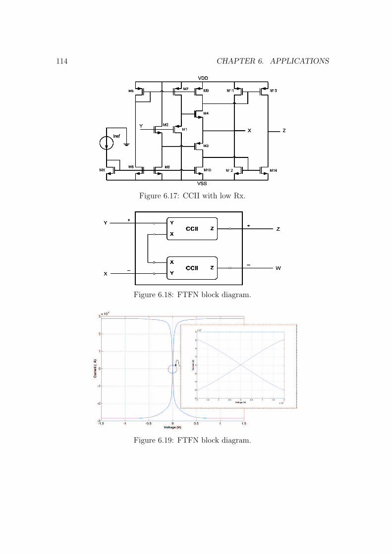
114 CHAPTER 6. APPLICATIONS
Figure 6.17: CCII with low Rx.
Figure 6.18: FTFN block diagram.
Figure 6.19: FTFN block diagram.
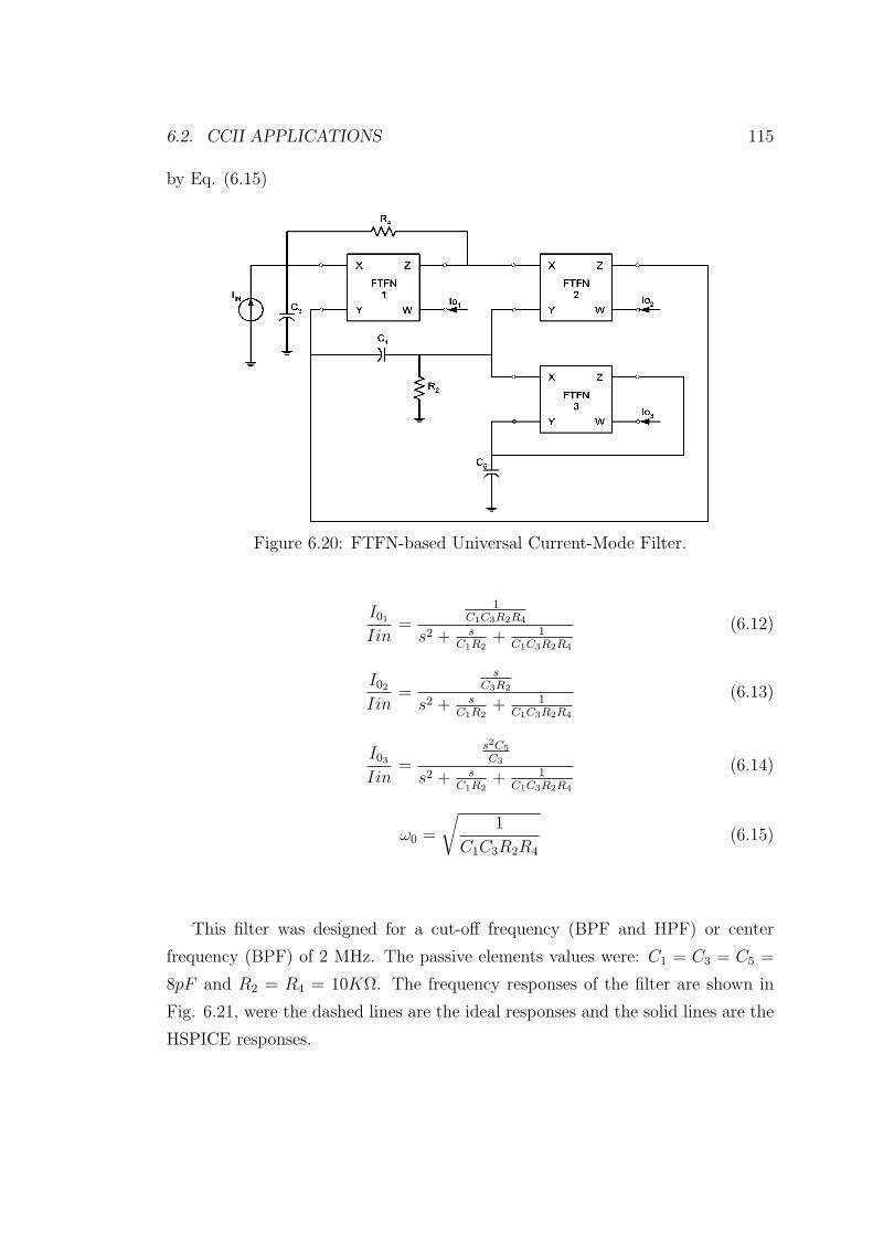
6.2. CCII APPLICATIONS 115
by Eq. (6.15)
Figure 6.20: FTFN-based Universal Current-Mode Filter.
I01
Iin=
1C1C3R2R4
s2 + sC1R2
+ 1C1C3R2R4
(6.12)
I02
Iin=
sC3R2
s2 + sC1R2
+ 1C1C3R2R4
(6.13)
I03
Iin=
s2C5
C3
s2 + sC1R2
+ 1C1C3R2R4
(6.14)
ω0 =
√1
C1C3R2R4
(6.15)
This filter was designed for a cut-off frequency (BPF and HPF) or center
frequency (BPF) of 2 MHz. The passive elements values were: C1 = C3 = C5 =
8pF and R2 = R4 = 10KΩ. The frequency responses of the filter are shown in
Fig. 6.21, were the dashed lines are the ideal responses and the solid lines are the
HSPICE responses.

116 CHAPTER 6. APPLICATIONS
Figure 6.21: FTFN-based Universal Current-Mode Filter AC response.
Sinusoidal Oscillator
In Fig. 6.22 is shown a single FTFN grounded capacitors sinusoidal oscillator [63].
The frequency and condition of oscillation are given by Eqs. (6.16) and (6.17),
respectively.
ω0 =
√R1(R4 + R6 + R7)
C3C8(R2R4R6R7)(6.16)
C3
R2R4
+C8
R2R4
=C8
R1R6
(6.17)
The oscillation frequency was chosen to be 2 MHz, so that the passive elements
values were: C3 = C8 = 64.5pF , R1 = 500Ω and R2 = R4 = R6 = R7 = 1KΩ.
The frequency of oscillation obtained in HSPICE is shown in Fig. 6.23.

6.2. CCII APPLICATIONS 117
Figure 6.22: FTFN-based Sinusoidal Oscillator.
Figure 6.23: FTFN-based Sinusoidal Oscillator AC response.
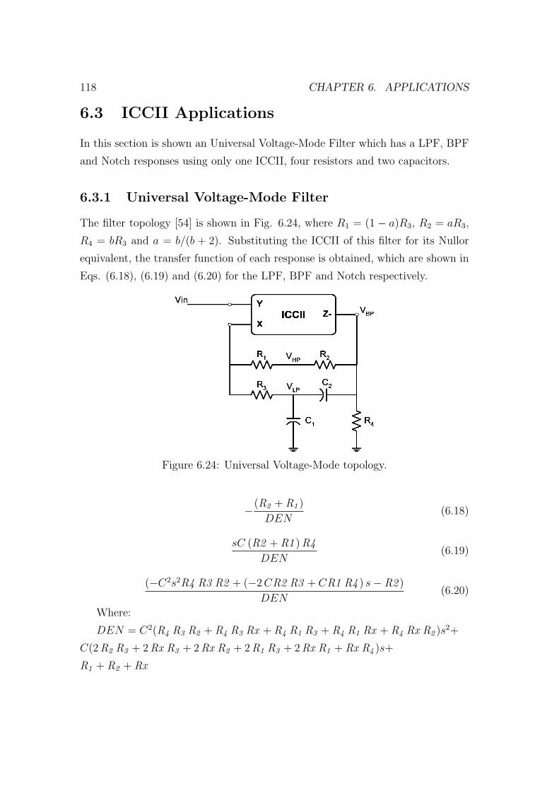
118 CHAPTER 6. APPLICATIONS
6.3 ICCII Applications
In this section is shown an Universal Voltage-Mode Filter which has a LPF, BPF
and Notch responses using only one ICCII, four resistors and two capacitors.
6.3.1 Universal Voltage-Mode Filter
The filter topology [54] is shown in Fig. 6.24, where R1 = (1 − a)R3, R2 = aR3,
R4 = bR3 and a = b/(b + 2). Substituting the ICCII of this filter for its Nullor
equivalent, the transfer function of each response is obtained, which are shown in
Eqs. (6.18), (6.19) and (6.20) for the LPF, BPF and Notch respectively.
Figure 6.24: Universal Voltage-Mode topology.
−(R2 + R1 )
DEN(6.18)
sC (R2 + R1 )R4
DEN(6.19)
(−C2s2R4 R3 R2 + (−2 CR2 R3 + CR1 R4 ) s− R2 )
DEN(6.20)
Where:
DEN = C2(R4 R3 R2 + R4 R3 Rx + R4 R1 R3 + R4 R1 Rx + R4 Rx R2 )s2+
C(2R2 R3 + 2Rx R3 + 2Rx R2 + 2R1 R3 + 2Rx R1 + Rx R4 )s+
R1 + R2 + Rx
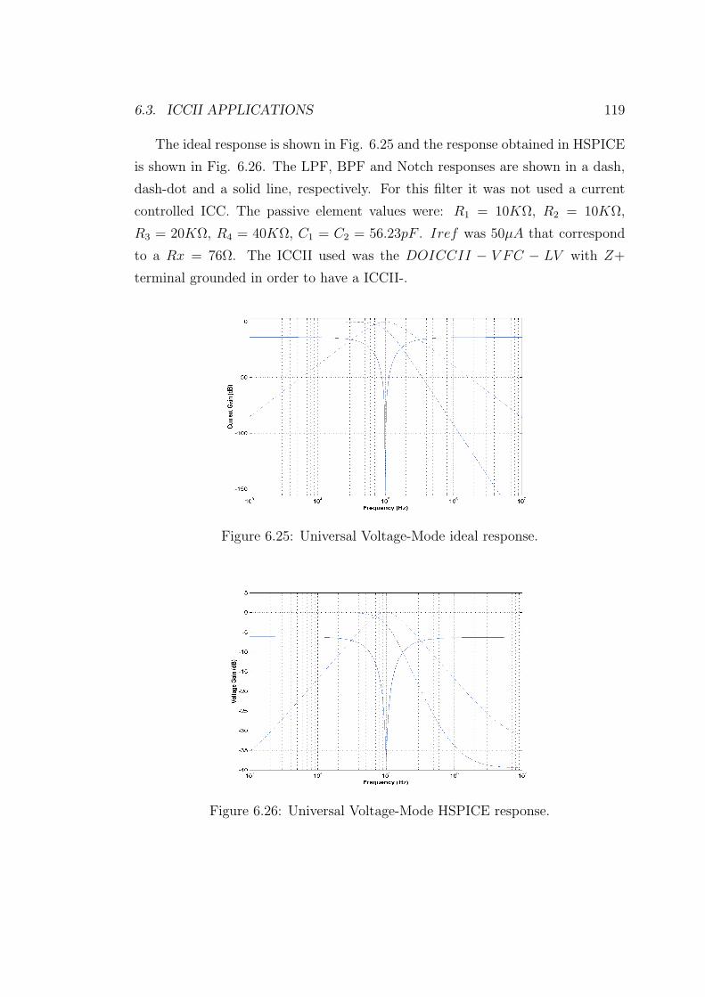
6.3. ICCII APPLICATIONS 119
The ideal response is shown in Fig. 6.25 and the response obtained in HSPICE
is shown in Fig. 6.26. The LPF, BPF and Notch responses are shown in a dash,
dash-dot and a solid line, respectively. For this filter it was not used a current
controlled ICC. The passive element values were: R1 = 10KΩ, R2 = 10KΩ,
R3 = 20KΩ, R4 = 40KΩ, C1 = C2 = 56.23pF . Iref was 50µA that correspond
to a Rx = 76Ω. The ICCII used was the DOICCII − V FC − LV with Z+
terminal grounded in order to have a ICCII-.
Figure 6.25: Universal Voltage-Mode ideal response.
Figure 6.26: Universal Voltage-Mode HSPICE response.

120 CHAPTER 6. APPLICATIONS
Chapter 7
Conclusions
A CC is a minimum 3-terminals device which can perform many useful analog
signal processing functions. The CC is not a new electronic block, since it was
first designed in 1969, but it is recently seen as a good alternative for Current-
Mode design in order to deal with Voltage-Mode problems.
As a first design step, a CC can be easily designed by combining and by
connecting the four UGCs (VF, VM, CF and CM) as basic construction blocks.
From the characteristic equation of each CC, they can be constructed just by
superimposing or by cascading the different UGCs in order to accomplish it.
The nullor is a very useful concept that helps the designer to easily analyze
a given element, circuit or system. The CCII nullor equivalent was taken from
literature, but the CCI and CCIII nullor equivalents were contributions of this
work. So, using this ideal concept it was easy to analyze a CC-based circuit in
order to obtain their characteristics equations. Although the nullor was used to
analyze ideally CC-based circuits, the parasitic resistance at the X-terminal of
each CC was included as it is a term that strongly modifies the CC behavior,
permitting to obtain CCCs.
Once a CC based in the UGCs blocks was designed, and taking the nullor as
a powerful analyzing ideal tool, each UGC can be designed in a transistor level.
Each UGC was designed as a symmetrical type circuit. Once this was done, each
CC can be implemented, just by interconnecting these UGCs. When these blocks
are connected between them to form a CC, their dimensions can be modified in
121
122 CHAPTER 7. CONCLUSIONS
order to have a better performance, but once we have this improved UGCs, they
can be taken as a fixed block to change from one type of CC to another one,
without any modification, just by interconnecting them as it was done in Chapter
2. These easy way to construct a CC is a contribution of this work. So, based
on this, all CCs topologies were designed in a transistor level, including the ICCI
and ICCIII which are contributions too.
Finally some implementations were shown where the better performances comes
from the CCII types. As it can be seen CCI and ICCII have some behavior prob-
lems due to the fact that ideal and HSPICE results doesn’t match at all.
7.1 Lines of Future Work
Once it was designed all CCs topologies, a future work proposed is:
• Optimization of all CC topologies in order to have better performances
in the CC applications.
• Design very low voltage CC, based in the CMs designed in [64] for very
low voltage applications.
• Design filtering, oscillation and inductor simulator applications for ICCI
and ICCIII topologies in order to investigate their suitability for a real im-
plementation.
• Improve the Rx value in order to reach lower levels and have CCs closer
to the ideal behavior.
• Investigate new VFs topologies due to the fact that most of the electrical
parameters depends on this UGC. More over, the VM depends on the VF
topology.
• Exploration on the transformation of CCI-based circuits to either or
both CCII-based and CCIII-based circuits. Also among ICCI-based, ICCII-
basec and ICCIII-based circuits.
Published Papers
1. E. Tlelo-Cuautle, D. Moro-Frıas, C. Sanchez-Lopez, M. A. Duarte-Villasenor,
Synthesis of CCII-s by superimposing VFs and CFs through genetic oper-
ations, IEICE Electronics Express, Vol. 5, No. 11, Pp: 411-417. June
2008.
2. D. Moro-Frıas, E. Tlelo-Cuautle, M. Fakhfakh, Design of CCI-based tuneable
active filters and sinusoidal oscillator, IEEE ICCDCS, ISBN 978-1-4244-
1957-9, Cancun, Mexico, April 28-30, 2008.
123

124 CHAPTER 7. CONCLUSIONS
Appendix A
MOS Transistor Characteristics
In today’s IC industry, a solid understanding of semiconductor devices is essential,
more so in analog design where transistors are not considered as simple switches
and many of their second-order effects impact the circuits performances. This
effects become more significant as IC technology scales the devices [19].
A.1 Threshold Voltage
Considering a NMOS transistor connected as it is shown in Fig. A.1, the gate
and the substrate form a capacitor, and as the voltage in gate terminal (VG)
becomes more positive, the holes in the p-substrate becomes repelled from the
gate area, leaving negative ions behind, generating a depletion region, where no
current flows because no charge carriers are available. As VG increases, the width
of the depletion region and the potential at the oxide-silicon interface increase too.
When the interface potential reaches a sufficiently positive value, electrons flow
from the source terminal to the interface and eventually to the drain terminal. The
VG for which this occurs is called ”Threshold Voltage” (VTH), where a channel of
charge carriers is formed under the gate oxide, between source and drain terminal
and the transistor is turned on. If VG increases further, the charge in the depletion
region remains relatively constant while the channel charge density continues to
increase, providing a greater current from source to drain terminals [19].
The gate and body form a parallel-plate capacitor with the oxide layer acting
125
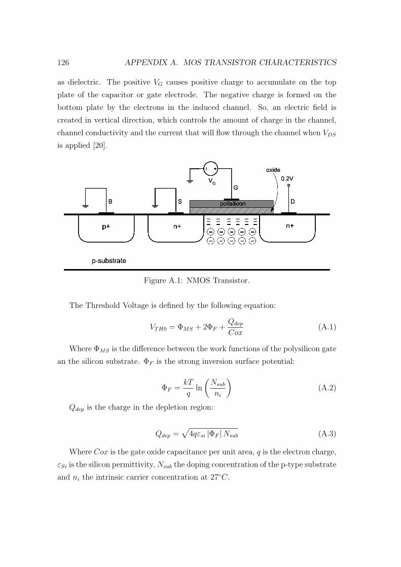
126 APPENDIX A. MOS TRANSISTOR CHARACTERISTICS
as dielectric. The positive VG causes positive charge to accumulate on the top
plate of the capacitor or gate electrode. The negative charge is formed on the
bottom plate by the electrons in the induced channel. So, an electric field is
created in vertical direction, which controls the amount of charge in the channel,
channel conductivity and the current that will flow through the channel when VDS
is applied [20].
Figure A.1: NMOS Transistor.
The Threshold Voltage is defined by the following equation:
VTH0 = ΦMS + 2ΦF +Qdep
Cox(A.1)
Where ΦMS is the difference between the work functions of the polysilicon gate
an the silicon substrate. ΦF is the strong inversion surface potential:
ΦF =kT
qln
(Nsub
ni
)(A.2)
Qdep is the charge in the depletion region:
Qdep =√
4qεsi |ΦF |Nsub (A.3)
Where Cox is the gate oxide capacitance per unit area, q is the electron charge,
εSi is the silicon permittivity, Nsub the doping concentration of the p-type substrate
and ni the intrinsic carrier concentration at 27C.
A.2. CMOS TRANSISTOR REGIONS 127
For real situations, the threshold value obtained from the above equation may
not be suited to circuit design, for this reason it is typically adjusted by implan-
tation of dopants into the channel area during device fabrication, altering the
doping level of the substrate near the oxide interface [19]. Standard practice is
to implant the proper type of ions into the substrate in the channel region to
adjust the threshold voltage to the desired value. This type of CMOS transistor
are also called Enhancement-type MOSFET [20], and are the kind of transistor
that will be used in this work. If the opposite impurities are implanted in the
channel region of the substrate, the threshold for an n-channel transistor can be
made negative. This type of transistor are called Depletion-type MOSFET and
can have current flow between drain and source terminals for zero values of the
gate-source voltage (VGS) [21].
A.2 CMOS Transistor Regions
There are various regions of operation of the MOS transistor, which depends on
the value of VGS − VTH . The first region is where VGS − VTH is equal to zero
or negative, so the transistor is in the Cutoff region. In Cutoff region the drain
current iD = 0A and VGS − VTH < 0.
When the transistor channel is formed between drain and source terminals, the
drain current iD can flow between this two terminals. The dependence of this
current can be developed by considering the characteristics of an incremental
length of the channel dy. This is illustrated in Fig. A.2:

128 APPENDIX A. MOS TRANSISTOR CHARACTERISTICS
Figure A.2: NMOS Transistor.
Where W is the transistor width (into the page) and the voltage VDS is small.
The resistance in the channel per unit of length dy can be written as:
dR =dy
µnQI(y)W(A.4)
Where µn is the average mobility of the electrons. The voltage drop, referenced
to the source, along the channel in the y direction is:
dv(y) = iDdR =iDdy
µnQI(y)W(A.5)
The charge per unit area in the channel QI(y) is given by the following Eq.
(A.6):
QI(y) = Cox [VGS − V (y)− VTH ] (A.6)
Substituting Eq. (A.6) into Eq. (A.5) and reordering is obtained:
iDdy = WµnCox [VGS − V (y)− VTH ] dV (y) (A.7)
Integrating Eq. (A.7) along the channel:
∫ L
0
iDdy =
∫ VDS
0
WµnCox [VGS − V (y)− VTH ] dV (y) (A.8)
Solving Eq. (A.8):
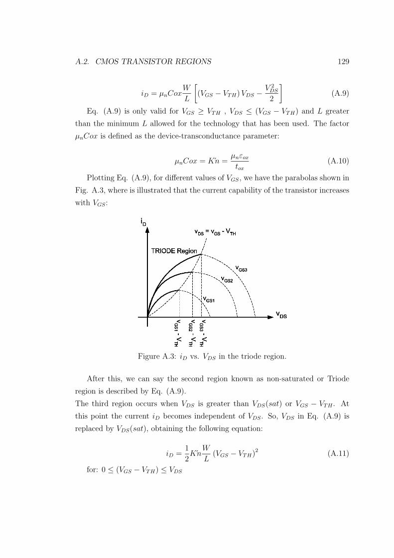
A.2. CMOS TRANSISTOR REGIONS 129
iD = µnCoxW
L
[(VGS − VTH) VDS − V 2
DS
2
](A.9)
Eq. (A.9) is only valid for VGS ≥ VTH , VDS ≤ (VGS − VTH) and L greater
than the minimum L allowed for the technology that has been used. The factor
µnCox is defined as the device-transconductance parameter:
µnCox = Kn =µnεox
tox
(A.10)
Plotting Eq. (A.9), for different values of VGS, we have the parabolas shown in
Fig. A.3, where is illustrated that the current capability of the transistor increases
with VGS:
Figure A.3: iD vs. VDS in the triode region.
After this, we can say the second region known as non-saturated or Triode
region is described by Eq. (A.9).
The third region occurs when VDS is greater than VDS(sat) or VGS − VTH . At
this point the current iD becomes independent of VDS. So, VDS in Eq. (A.9) is
replaced by VDS(sat), obtaining the following equation:
iD =1
2Kn
W
L(VGS − VTH)2 (A.11)
for: 0 ≤ (VGS − VTH) ≤ VDS

130 APPENDIX A. MOS TRANSISTOR CHARACTERISTICS
The iD current does not follow the parabolic behavior for the previous relation
(Eq. (A.4)), in fact this current becomes relatively constant in the third region,
known as Saturation region. That is, from Eq. (A.6) the local density of inversion
layer charge is proportional to VGS − V (y) − VTH . Thus, if V (y) approaches
VGS − VTH , then QI(y) drops to zero. That is, as shown in Fig. A.4, if VDS is
slightly greater than VDS(sat), then the inversion layer stops at y < L, and it is
said the channel is ”pinched off”, shown in Fig. A.5. As VDS increases more, the
point at which QI equals zero gradually moves toward the source. So, taken Eq.
(A.8) for a saturated device, and since QI is the density of mobile charge, the
integral on the left-hand side must be taken from y = 0 to y = L′, where L′ is
the point at which QI drops to zero, and on the right-hand side from V (y) = 0 to
V (y) = VGS − VTH . As a result:
iD =1
2Kn
W
L′ (VGS − VTH)2 (A.12)
Figure A.4: iD vs. VDS in the saturation region.
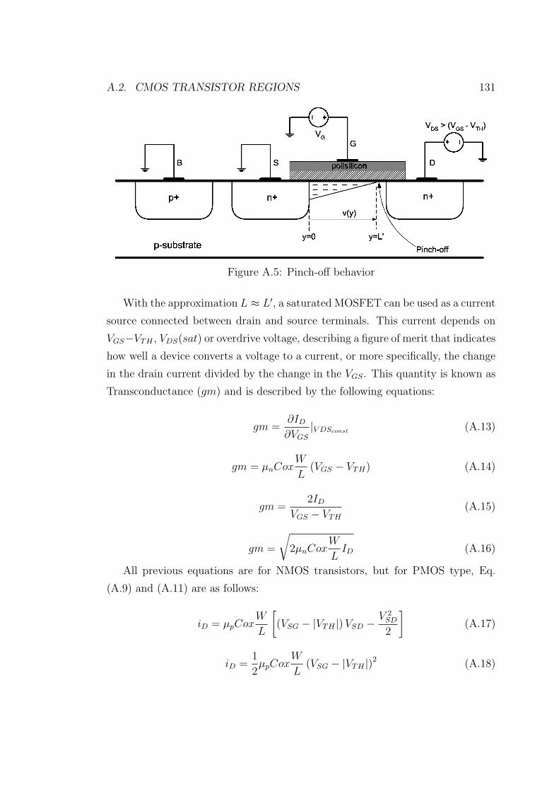
A.2. CMOS TRANSISTOR REGIONS 131
Figure A.5: Pinch-off behavior
With the approximation L ≈ L′, a saturated MOSFET can be used as a current
source connected between drain and source terminals. This current depends on
VGS−VTH , VDS(sat) or overdrive voltage, describing a figure of merit that indicates
how well a device converts a voltage to a current, or more specifically, the change
in the drain current divided by the change in the VGS. This quantity is known as
Transconductance (gm) and is described by the following equations:
gm =∂ID
∂VGS
|V DSconst (A.13)
gm = µnCoxW
L(VGS − VTH) (A.14)
gm =2ID
VGS − VTH
(A.15)
gm =
√2µnCox
W
LID (A.16)
All previous equations are for NMOS transistors, but for PMOS type, Eq.
(A.9) and (A.11) are as follows:
iD = µpCoxW
L
[(VSG − |VTH |) VSD − V 2
SD
2
](A.17)
iD =1
2µpCox
W
L(VSG − |VTH |)2 (A.18)

132 APPENDIX A. MOS TRANSISTOR CHARACTERISTICS
Therefore, VGS becomes VSG, VDS becomes VSD, VTHn becomes −VTHp, and
so on. In PMOS transistor the Threshold voltage is negative, so the condition to
keep this transistor in saturation region is now VSD > VSG − |VTHp|, and the iD
current now flows from the source to the drain terminals.
A.3 Second-Order Effects
In this section are described two of the most important second-order effects that
directly impact in analog design.
A.3.1 Body Effect
The Body Effect directly impact in an increment of the Threshold Voltage level.
Is common to see some applications with the substrate terminal connected to
the source terminal, where a pn junction is formed between the substrate and
the induced channel, generating a constant zero bias or cut-off, and as a conse-
quence, the Threshold Voltage does not change its value. In integrated circuits the
substrate, which is common to many MOS transistors, is connected to the most
negative (NMOS) or most positive (PMOS) power supply, in order to maintain
the cut-off condition for all the substrate-to-channel junctions, but this reverse
bias voltage between source and substrate (VSB) will have an effect on the device
operation [20]. Lets consider a NMOS transistor with its substrate terminal more
negative than its source terminal. As a consequence of the reverse bias voltage,
the depletion region becomes wider, reducing the channel depth. So, in order to
return the channel to its former state, VGS has to be increased.
From Eq. (A.1) it is clear that the Threshold Voltage is function of the total
charge in the depletion region because the gate charge must mirror QI before an
inversion layer is formed [19]. There for, as VSB increase, VTH will do the same.
After this, the Threshold Voltage in a MOSFET is given by:
VTH = VTH0 + γ[√
|2ΦF + VSB| −√|2ΦF |
](A.19)
Where VTH0 is the same Threshold Voltage for VSB = 0 given in Eq. (A.1),

A.3. SECOND-ORDER EFFECTS 133
ΦF is the strong inversion surface potential described by Eq. (A.2) and γ is a
fabrication process parameter known as body-effect parameter, which is given by:
γ =
√2qNsubεSI
Cox(A.20)
Eq. (A.20) shows that an incremental change in VSB generates an incremental
change in VTH which results in an incremental change in iD. Due to this, substrate
terminal acts as another gate for the transistor [20].
A.3.2 Channel Modulation Effect
As it was seen before, the channel length gradually decreases as the potential
difference between gate and drain terminals increases (VDS), in other words, as VDS
increase beyond VDS(sat), the channel pinch-off point is moved slightly away from
the drain toward the source. The voltage across the channel is constant VDS(sat) =
(VGS−VTH), and the additional voltage applied to the drain terminal appears as a
voltage drop across the narrow depletion region between the channel and the drain
diffusion, accelerating the electrons that reach the end of the channel, sweeping
them across the depletion region into the drain. This is better explained by Fig.
A.6:
Figure A.6: Channel Modulation behavior.
If L′ = L−∆L, reordering this, is obtained:
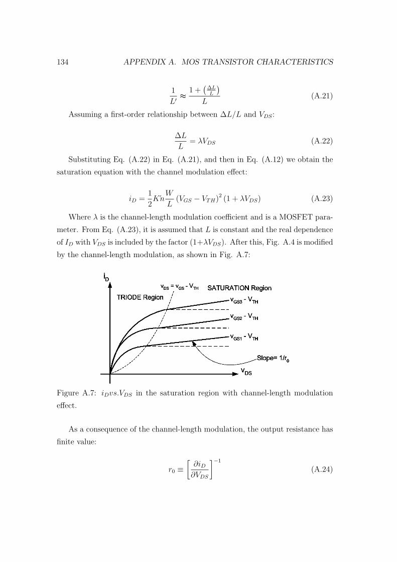
134 APPENDIX A. MOS TRANSISTOR CHARACTERISTICS
1
L′≈
1 +(
∆LL
)
L(A.21)
Assuming a first-order relationship between ∆L/L and VDS:
∆L
L= λVDS (A.22)
Substituting Eq. (A.22) in Eq. (A.21), and then in Eq. (A.12) we obtain the
saturation equation with the channel modulation effect:
iD =1
2Kn
W
L(VGS − VTH)2 (1 + λVDS) (A.23)
Where λ is the channel-length modulation coefficient and is a MOSFET para-
meter. From Eq. (A.23), it is assumed that L is constant and the real dependence
of ID with VDS is included by the factor (1+λVDS). After this, Fig. A.4 is modified
by the channel-length modulation, as shown in Fig. A.7:
Figure A.7: iDvs.VDS in the saturation region with channel-length modulation
effect.
As a consequence of the channel-length modulation, the output resistance has
finite value:
r0 ≡[
∂iD∂VDS
]−1
(A.24)

A.3. SECOND-ORDER EFFECTS 135
r0 =
[λ
Kn
2
W
L(VGS − VTH)2
]−1
(A.25)

136 APPENDIX A. MOS TRANSISTOR CHARACTERISTICS

Appendix B
CCs transistor level topologies
B.1 CCs
B.1.1 CCIs
Figure B.1: DOCCI-VFA-S
137

138 APPENDIX B. CCS TRANSISTOR LEVEL TOPOLOGIES
Figure B.2: DOCCI-VFB-S
Figure B.3: DOCCI-VFC-S
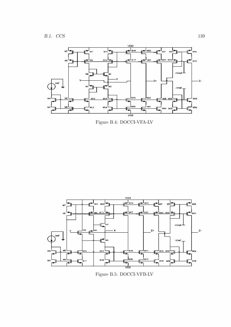
B.1. CCS 139
Figure B.4: DOCCI-VFA-LV
Figure B.5: DOCCI-VFB-LV
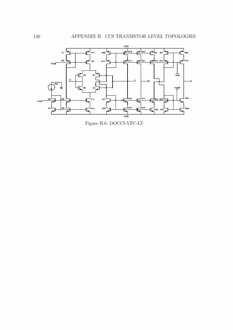
140 APPENDIX B. CCS TRANSISTOR LEVEL TOPOLOGIES
Figure B.6: DOCCI-VFC-LV
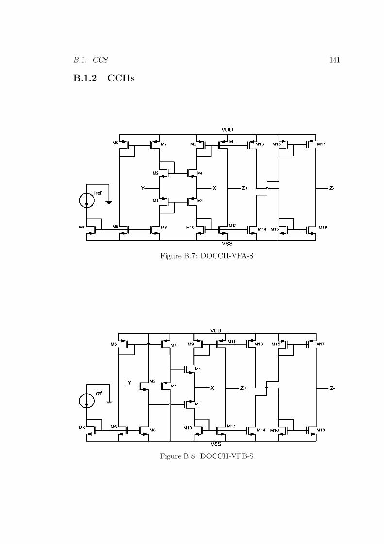
B.1. CCS 141
B.1.2 CCIIs
Figure B.7: DOCCII-VFA-S
Figure B.8: DOCCII-VFB-S
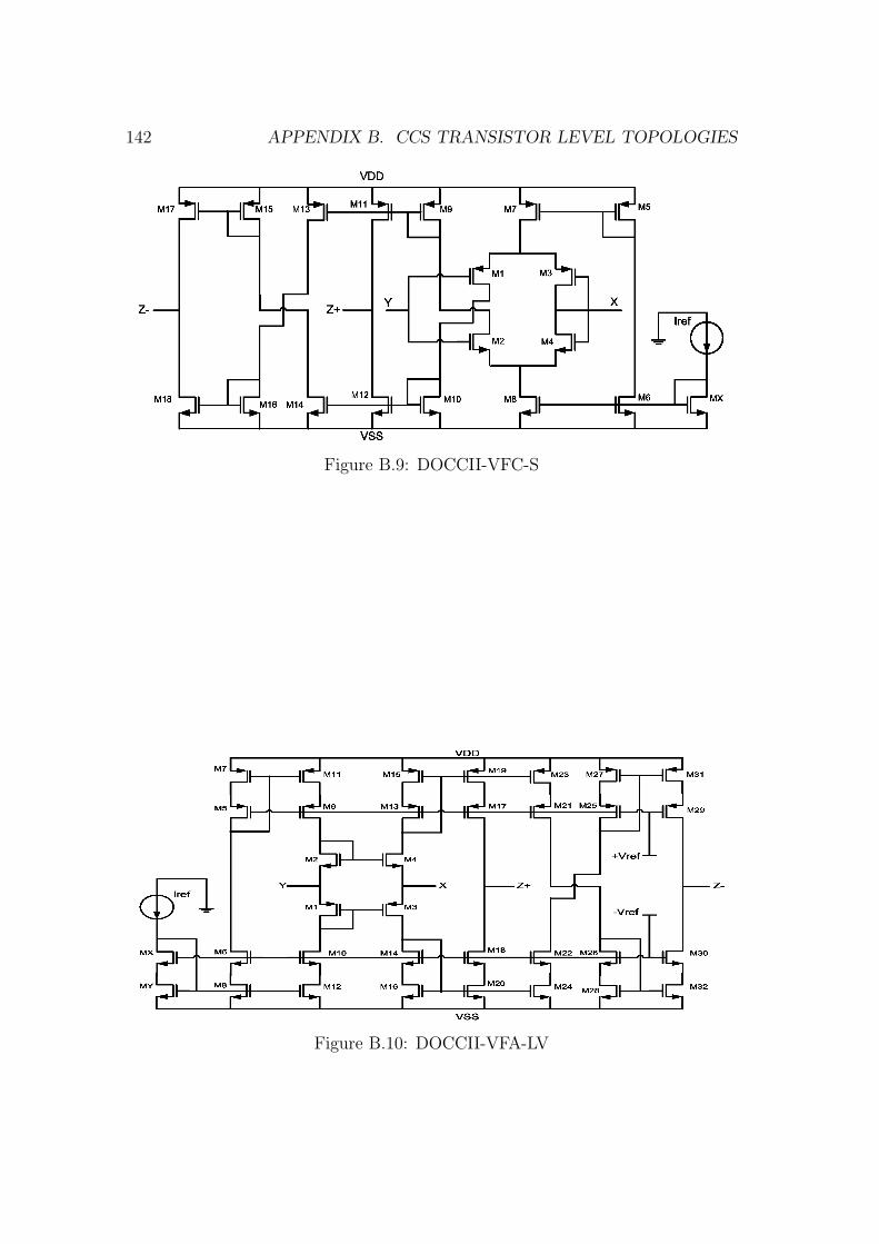
142 APPENDIX B. CCS TRANSISTOR LEVEL TOPOLOGIES
Figure B.9: DOCCII-VFC-S
Figure B.10: DOCCII-VFA-LV
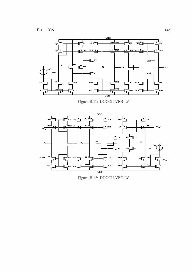
B.1. CCS 143
Figure B.11: DOCCII-VFB-LV
Figure B.12: DOCCII-VFC-LV
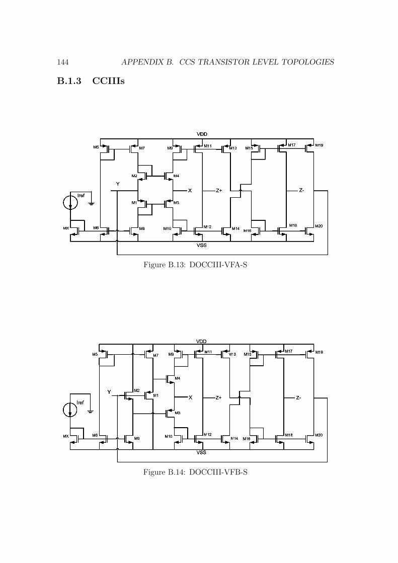
144 APPENDIX B. CCS TRANSISTOR LEVEL TOPOLOGIES
B.1.3 CCIIIs
Figure B.13: DOCCIII-VFA-S
Figure B.14: DOCCIII-VFB-S
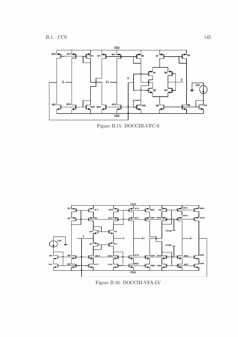
B.1. CCS 145
Figure B.15: DOCCIII-VFC-S
Figure B.16: DOCCIII-VFA-LV
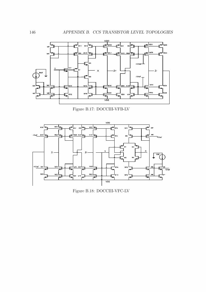
146 APPENDIX B. CCS TRANSISTOR LEVEL TOPOLOGIES
Figure B.17: DOCCIII-VFB-LV
Figure B.18: DOCCIII-VFC-LV

B.2. ICCS 147
B.2 ICCs
B.2.1 ICCIs
Figure B.19: DOICCI-VMA-S
Figure B.20: DOICCI-VMB-S

148 APPENDIX B. CCS TRANSISTOR LEVEL TOPOLOGIES
Figure B.21: DOICCI-VMC-S
Figure B.22: DOICCI-VMA-LV
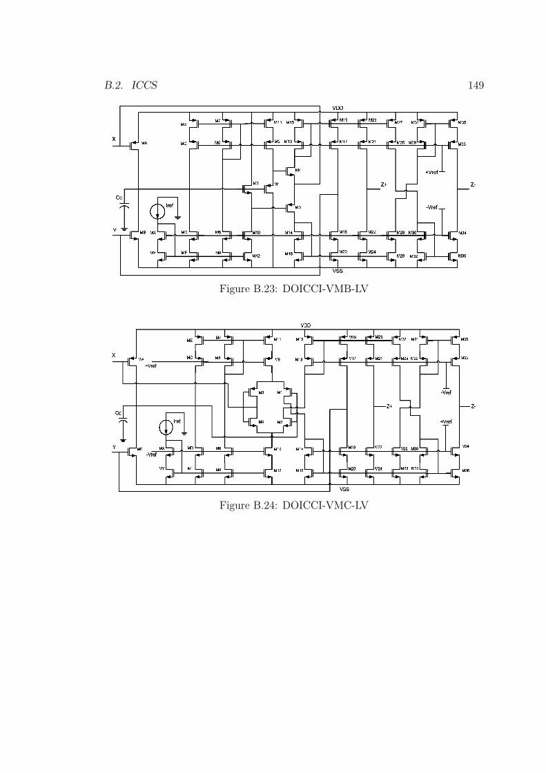
B.2. ICCS 149
Figure B.23: DOICCI-VMB-LV
Figure B.24: DOICCI-VMC-LV
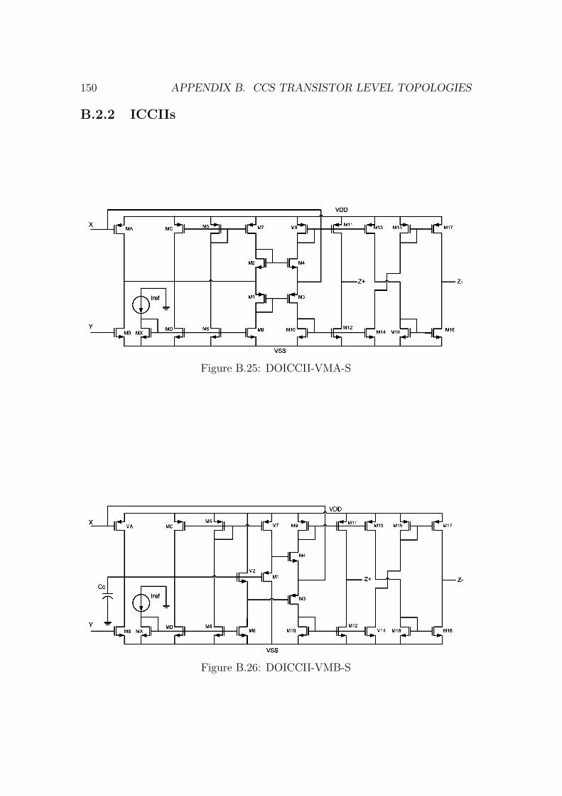
150 APPENDIX B. CCS TRANSISTOR LEVEL TOPOLOGIES
B.2.2 ICCIIs
Figure B.25: DOICCII-VMA-S
Figure B.26: DOICCII-VMB-S
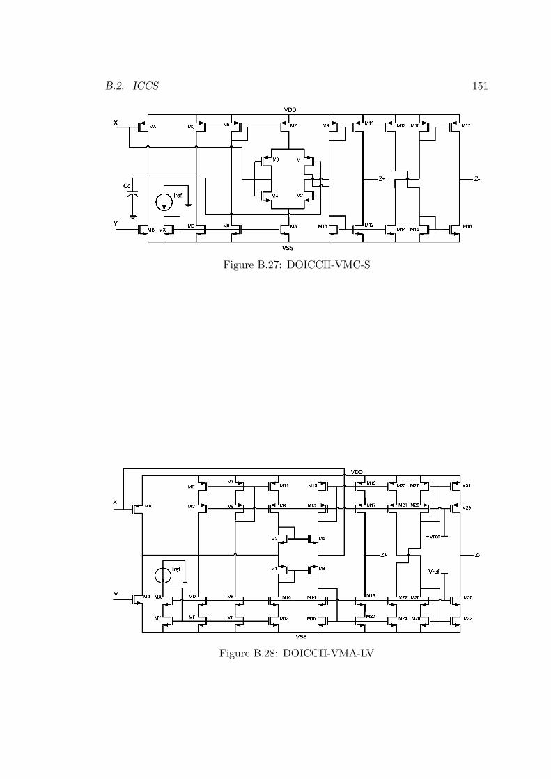
B.2. ICCS 151
Figure B.27: DOICCII-VMC-S
Figure B.28: DOICCII-VMA-LV

152 APPENDIX B. CCS TRANSISTOR LEVEL TOPOLOGIES
Figure B.29: DOICCII-VMB-LV
Figure B.30: DOICCII-VMC-LV

B.2. ICCS 153
B.2.3 ICCIIIs
Figure B.31: DOICCIII-VMA-S
Figure B.32: DOICCIII-VMB-S

154 APPENDIX B. CCS TRANSISTOR LEVEL TOPOLOGIES
Figure B.33: DOICCIII-VMC-S
Figure B.34: DOICCIII-VMA-LV
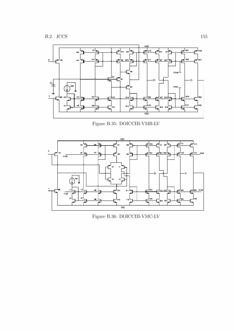
B.2. ICCS 155
Figure B.35: DOICCIII-VMB-LV
Figure B.36: DOICCIII-VMC-LV

156 APPENDIX B. CCS TRANSISTOR LEVEL TOPOLOGIES

List of Figures
1.1 Different types of CCs. . . . . . . . . . . . . . . . . . . . . . . . . 4
1.2 First Bipolar CC. . . . . . . . . . . . . . . . . . . . . . . . . . . . 5
2.1 First Generation CC. . . . . . . . . . . . . . . . . . . . . . . . . . 8
2.2 Block diagram of: (a)CCI+ and (b) CCI-. . . . . . . . . . . . . . 10
2.3 Block diagram of: (A) ICCI+ and (b) ICCI- . . . . . . . . . . . . 11
2.4 Block diagram of: (a) MOCCI and (b) MOICCI. . . . . . . . . . . 12
2.5 Block diagram of: (a) ICCCI+, (b) CCCI- and (c)MOICCCI. . . 13
2.6 Block diagram of: (a) CCII+ and (b) CCII-. . . . . . . . . . . . . 14
2.7 Block diagram of (a) ICCII+ and (b) ICCII-. . . . . . . . . . . . 15
2.8 Block diagram of: (a) MOCCII and (b) MOICCII. . . . . . . . . . 16
2.9 Block diagram of: (a) ICCCII+, (b) CCCII- and (c) MOICCCII. . 16
2.10 Block diagram of: (a) CCIII+ and (b) CCIII-. . . . . . . . . . . . 18
2.11 Block diagram of (a) ICCIII+ and (b) ICCIII-. . . . . . . . . . . 19
2.12 Block diagram of: (a) MOCCIII and (b) MOICCIII. . . . . . . . . 19
2.13 Block diagram of: (a) ICCCIII, (b) CCCIII- and (c)MOICCCIII. 20
3.1 Nullor symbol. . . . . . . . . . . . . . . . . . . . . . . . . . . . . 22
3.2 Basic nullor equivalents. . . . . . . . . . . . . . . . . . . . . . . . 22
3.3 Nullor equivalents: (a) Diode, (b) BJT, (c) MOSFET, (d) VS. . . 23
3.4 Nullor equivalents: (a) VCVS, (b) VCCS, (c) CCVS, (d) CCCS. . 24
3.5 Nullor equivalents: (a) Opamp, (b) OTA, (c) OTRA, (d) COA. . 25
3.6 Nullor equivalents: (a) CCI+, (b) CCI-, (c) ICCI+, (d) ICCI-, (e)
MOICCI. . . . . . . . . . . . . . . . . . . . . . . . . . . . . . . . 26
157

158 LIST OF FIGURES
3.7 Nullor equivalents: (a) CCII+, (b) CCII-, (c) ICCII+, (d) ICCII-,
(e) MOCCII. . . . . . . . . . . . . . . . . . . . . . . . . . . . . . 28
3.8 Nullor equivalents: (a) CCIII+, (b) CCIII-, (c) ICCIII+, (d) ICCII-
, (e) MOICCIII. . . . . . . . . . . . . . . . . . . . . . . . . . . . . 29
3.9 (a) CCI+ and (b) Nullor equivalent of (a). . . . . . . . . . . . . . 32
3.10 (a) CCI+ and (b) Nullor equivalent of (a). . . . . . . . . . . . . . 34
3.11 (a) ICCI+ and (b) Nullor equivalent of (a). . . . . . . . . . . . . . 36
3.12 (a) ICCI+ and (b) Nullor equivalent of (a). . . . . . . . . . . . . . 37
3.13 (a) ICCIII- and (b) Nullor equivalent of (a). . . . . . . . . . . . . 38
3.14 (a) ICCIII- and (b) Nullor equivalent of (a). . . . . . . . . . . . . 40
3.15 Current-mode DOCCII-based universal filter topology. . . . . . . 41
3.16 Nullor equivalent of current-mode DOCCII-based universal filter. 42
3.17 Ideal responses of the current-mode universal filter. . . . . . . . . 43
4.1 Voltage Followers: (a) VF-A, (b) VF-B and (c) VF-C. . . . . . . . 46
4.2 VF-A. . . . . . . . . . . . . . . . . . . . . . . . . . . . . . . . . . 47
4.3 VF-A with node voltages. . . . . . . . . . . . . . . . . . . . . . . 47
4.4 VF-B. . . . . . . . . . . . . . . . . . . . . . . . . . . . . . . . . . 49
4.5 VF-B with node voltages. . . . . . . . . . . . . . . . . . . . . . . 50
4.6 VF-C. . . . . . . . . . . . . . . . . . . . . . . . . . . . . . . . . . 51
4.7 VF-C with node voltages. . . . . . . . . . . . . . . . . . . . . . . 52
4.8 NMOS Current Mirror. . . . . . . . . . . . . . . . . . . . . . . . . 54
4.9 Simple Current Mirror. . . . . . . . . . . . . . . . . . . . . . . . . 55
4.10 Low Voltage Current Mirror. . . . . . . . . . . . . . . . . . . . . . 56
4.11 (a) Cascode and (b) Wilson Current Mirrors. . . . . . . . . . . . . 57
4.12 Voltage Mirror. . . . . . . . . . . . . . . . . . . . . . . . . . . . . 58
4.13 Voltage Mirror: (a) VM-A, (b) VM-B and (c) VM-C. . . . . . . . 59
4.14 Current Mirror based Current Follower. . . . . . . . . . . . . . . . 61
4.15 (a) Simple and (b) Low Voltage Current Followers. . . . . . . . . 62
5.1 DOCCI structure. . . . . . . . . . . . . . . . . . . . . . . . . . . . 64
5.2 DOCCI-VFA-S . . . . . . . . . . . . . . . . . . . . . . . . . . . . 65
5.3 DOCCI-VFA-LV . . . . . . . . . . . . . . . . . . . . . . . . . . . 66
LIST OF FIGURES 159
5.4 DOCCI structure. . . . . . . . . . . . . . . . . . . . . . . . . . . . 71
5.5 DOCCII-VFB-S . . . . . . . . . . . . . . . . . . . . . . . . . . . . 72
5.6 DOCCIII structure. . . . . . . . . . . . . . . . . . . . . . . . . . . 77
5.7 DOCCIII-VFC-S . . . . . . . . . . . . . . . . . . . . . . . . . . . 78
5.8 DOICCI structure. . . . . . . . . . . . . . . . . . . . . . . . . . . 84
5.9 DOICCI-VMA-S . . . . . . . . . . . . . . . . . . . . . . . . . . . 84
5.10 DOICCII structure. . . . . . . . . . . . . . . . . . . . . . . . . . . 89
5.11 DOICCII-VMB-S . . . . . . . . . . . . . . . . . . . . . . . . . . . 89
5.12 DOICCIII structure. . . . . . . . . . . . . . . . . . . . . . . . . . 94
5.13 DOICCIII-VMC-S . . . . . . . . . . . . . . . . . . . . . . . . . . 94
5.14 CCs parasitics elements. . . . . . . . . . . . . . . . . . . . . . . . 99
6.1 CCI-based BPF Filter . . . . . . . . . . . . . . . . . . . . . . . . 102
6.2 BPF filter AC response. . . . . . . . . . . . . . . . . . . . . . . . 103
6.3 CCI-based BPF Filter . . . . . . . . . . . . . . . . . . . . . . . . 103
6.4 HPF filter AC response. . . . . . . . . . . . . . . . . . . . . . . . 104
6.5 CCI-based Sinusoidal Oscillator . . . . . . . . . . . . . . . . . . . 105
6.6 Oscillator AC response for 1.8 MHz. . . . . . . . . . . . . . . . . . 106
6.7 Oscillator AC response for 3.5 MHz. . . . . . . . . . . . . . . . . . 106
6.8 DOCCI-VFA-SCM Rx vs. Iref curve. . . . . . . . . . . . . . . . . 107
6.9 Universal current-mode AC response. . . . . . . . . . . . . . . . . 108
6.10 fifth-order LPF. . . . . . . . . . . . . . . . . . . . . . . . . . . . . 109
6.11 DOCCII-based Floated Inductance Simulator. . . . . . . . . . . . 110
6.12 Floated Inductance Simulator 1 AC response. . . . . . . . . . . . 110
6.13 DOCCII-VFC-SCM Rx vs. Iref curve. . . . . . . . . . . . . . . . 110
6.14 DOCCII-based Floated Inductance Simulator 2. . . . . . . . . . . 111
6.15 Floated Inductance Simulator 2 AC response. . . . . . . . . . . . 112
6.16 DOCCII-VFB-LV Rx vs. Iref curve. . . . . . . . . . . . . . . . . . 112
6.17 CCII with low Rx. . . . . . . . . . . . . . . . . . . . . . . . . . . 114
6.18 FTFN block diagram. . . . . . . . . . . . . . . . . . . . . . . . . . 114
6.19 FTFN block diagram. . . . . . . . . . . . . . . . . . . . . . . . . . 114
6.20 FTFN-based Universal Current-Mode Filter. . . . . . . . . . . . . 115
160 LIST OF FIGURES
6.21 FTFN-based Universal Current-Mode Filter AC response. . . . . . 116
6.22 FTFN-based Sinusoidal Oscillator. . . . . . . . . . . . . . . . . . 117
6.23 FTFN-based Sinusoidal Oscillator AC response. . . . . . . . . . . 117
6.24 Universal Voltage-Mode topology. . . . . . . . . . . . . . . . . . . 118
6.25 Universal Voltage-Mode ideal response. . . . . . . . . . . . . . . . 119
6.26 Universal Voltage-Mode HSPICE response. . . . . . . . . . . . . . 119
A.1 NMOS Transistor. . . . . . . . . . . . . . . . . . . . . . . . . . . 126
A.2 NMOS Transistor. . . . . . . . . . . . . . . . . . . . . . . . . . . 128
A.3 iD vs. VDS in the triode region. . . . . . . . . . . . . . . . . . . . 129
A.4 iD vs. VDS in the saturation region. . . . . . . . . . . . . . . . . . 130
A.5 Pinch-off behavior . . . . . . . . . . . . . . . . . . . . . . . . . . . 131
A.6 Channel Modulation behavior. . . . . . . . . . . . . . . . . . . . . 133
A.7 iDvs.VDS in the saturation region with channel-length modulation
effect. . . . . . . . . . . . . . . . . . . . . . . . . . . . . . . . . . 134
B.1 DOCCI-VFA-S . . . . . . . . . . . . . . . . . . . . . . . . . . . . 137
B.2 DOCCI-VFB-S . . . . . . . . . . . . . . . . . . . . . . . . . . . . 138
B.3 DOCCI-VFC-S . . . . . . . . . . . . . . . . . . . . . . . . . . . . 138
B.4 DOCCI-VFA-LV . . . . . . . . . . . . . . . . . . . . . . . . . . . 139
B.5 DOCCI-VFB-LV . . . . . . . . . . . . . . . . . . . . . . . . . . . 139
B.6 DOCCI-VFC-LV . . . . . . . . . . . . . . . . . . . . . . . . . . . 140
B.7 DOCCII-VFA-S . . . . . . . . . . . . . . . . . . . . . . . . . . . . 141
B.8 DOCCII-VFB-S . . . . . . . . . . . . . . . . . . . . . . . . . . . . 141
B.9 DOCCII-VFC-S . . . . . . . . . . . . . . . . . . . . . . . . . . . . 142
B.10 DOCCII-VFA-LV . . . . . . . . . . . . . . . . . . . . . . . . . . . 142
B.11 DOCCII-VFB-LV . . . . . . . . . . . . . . . . . . . . . . . . . . . 143
B.12 DOCCII-VFC-LV . . . . . . . . . . . . . . . . . . . . . . . . . . . 143
B.13 DOCCIII-VFA-S . . . . . . . . . . . . . . . . . . . . . . . . . . . 144
B.14 DOCCIII-VFB-S . . . . . . . . . . . . . . . . . . . . . . . . . . . 144
B.15 DOCCIII-VFC-S . . . . . . . . . . . . . . . . . . . . . . . . . . . 145
B.16 DOCCIII-VFA-LV . . . . . . . . . . . . . . . . . . . . . . . . . . 145
B.17 DOCCIII-VFB-LV . . . . . . . . . . . . . . . . . . . . . . . . . . 146

LIST OF FIGURES 161
B.18 DOCCIII-VFC-LV . . . . . . . . . . . . . . . . . . . . . . . . . . 146
B.19 DOICCI-VMA-S . . . . . . . . . . . . . . . . . . . . . . . . . . . 147
B.20 DOICCI-VMB-S . . . . . . . . . . . . . . . . . . . . . . . . . . . 147
B.21 DOICCI-VMC-S . . . . . . . . . . . . . . . . . . . . . . . . . . . 148
B.22 DOICCI-VMA-LV . . . . . . . . . . . . . . . . . . . . . . . . . . 148
B.23 DOICCI-VMB-LV . . . . . . . . . . . . . . . . . . . . . . . . . . . 149
B.24 DOICCI-VMC-LV . . . . . . . . . . . . . . . . . . . . . . . . . . . 149
B.25 DOICCII-VMA-S . . . . . . . . . . . . . . . . . . . . . . . . . . . 150
B.26 DOICCII-VMB-S . . . . . . . . . . . . . . . . . . . . . . . . . . . 150
B.27 DOICCII-VMC-S . . . . . . . . . . . . . . . . . . . . . . . . . . . 151
B.28 DOICCII-VMA-LV . . . . . . . . . . . . . . . . . . . . . . . . . . 151
B.29 DOICCII-VMB-LV . . . . . . . . . . . . . . . . . . . . . . . . . . 152
B.30 DOICCII-VMC-LV . . . . . . . . . . . . . . . . . . . . . . . . . . 152
B.31 DOICCIII-VMA-S . . . . . . . . . . . . . . . . . . . . . . . . . . 153
B.32 DOICCIII-VMB-S . . . . . . . . . . . . . . . . . . . . . . . . . . 153
B.33 DOICCIII-VMC-S . . . . . . . . . . . . . . . . . . . . . . . . . . 154
B.34 DOICCIII-VMA-LV . . . . . . . . . . . . . . . . . . . . . . . . . 154
B.35 DOICCIII-VMB-LV . . . . . . . . . . . . . . . . . . . . . . . . . . 155
B.36 DOICCIII-VMC-LV . . . . . . . . . . . . . . . . . . . . . . . . . . 155

162 LIST OF FIGURES
List of Tables
4.1 VFs electrical parameter measurements. . . . . . . . . . . . . . . 53
4.2 CMs electrical parameter measurements. . . . . . . . . . . . . . . 57
4.3 VMs electrical parameter measurements. . . . . . . . . . . . . . . 60
4.4 CFs electrical parameter measurements. . . . . . . . . . . . . . . 62
5.1 DOCCI channel width (W ) dimensions. . . . . . . . . . . . . . . . 67
5.2 DOCCI-VFA-S electrical parameter measurements . . . . . . . . . 68
5.3 DOCCI-VFB-S electrical parameter measurements . . . . . . . . . 68
5.4 DOCCI-VFC-S electrical parameter measurements . . . . . . . . . 69
5.5 DOCCI-VFA-LV electrical parameter measurements . . . . . . . . 69
5.6 DOCCI-VFB-LV electrical parameter measurements . . . . . . . . 70
5.7 DOCCI-VFC-LV electrical parameter measurements . . . . . . . . 70
5.8 DOCCII channel width (W ) dimensions. . . . . . . . . . . . . . . 73
5.9 DOCCII-VFA-S electrical parameter measurements . . . . . . . . 74
5.10 DOCCII-VFB-S electrical parameter measurements . . . . . . . . 74
5.11 DOCCII-VFC-S electrical parameter measurements . . . . . . . . 75
5.12 DOCCII-VFA-LV electrical parameter measurements . . . . . . . 75
5.13 DOCCII-VFB-LV electrical parameter measurements . . . . . . . 76
5.14 DOCCII-VFC-LV electrical parameter measurements . . . . . . . 76
5.15 DOCCIII channel width (W ) dimensions. . . . . . . . . . . . . . . 79
5.16 DOCCIII-VFA-S electrical parameter measurements . . . . . . . . 80
5.17 DOCCIII-VFB-S electrical parameter measurements . . . . . . . . 80
5.18 DOCCIII-VFC-S electrical parameter measurements . . . . . . . . 81
5.19 DOCCIII-VFA-LV electrical parameter measurements . . . . . . . 81
163
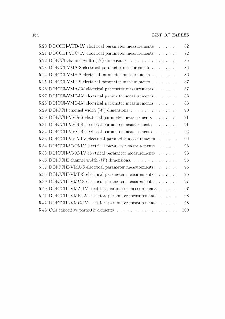
164 LIST OF TABLES
5.20 DOCCIII-VFB-LV electrical parameter measurements . . . . . . . 82
5.21 DOCCIII-VFC-LV electrical parameter measurements . . . . . . . 82
5.22 DOICCI channel width (W ) dimensions. . . . . . . . . . . . . . . 85
5.23 DOICCI-VMA-S electrical parameter measurements . . . . . . . . 86
5.24 DOICCI-VMB-S electrical parameter measurements . . . . . . . . 86
5.25 DOICCI-VMC-S electrical parameter measurements . . . . . . . . 87
5.26 DOICCI-VMA-LV electrical parameter measurements . . . . . . . 87
5.27 DOICCI-VMB-LV electrical parameter measurements . . . . . . . 88
5.28 DOICCI-VMC-LV electrical parameter measurements . . . . . . . 88
5.29 DOICCII channel width (W ) dimensions. . . . . . . . . . . . . . . 90
5.30 DOICCII-VMA-S electrical parameter measurements . . . . . . . 91
5.31 DOICCII-VMB-S electrical parameter measurements . . . . . . . 91
5.32 DOICCII-VMC-S electrical parameter measurements . . . . . . . 92
5.33 DOICCII-VMA-LV electrical parameter measurements . . . . . . 92
5.34 DOICCII-VMB-LV electrical parameter measurements . . . . . . 93
5.35 DOICCII-VMC-LV electrical parameter measurements . . . . . . 93
5.36 DOICCIII channel width (W ) dimensions. . . . . . . . . . . . . . 95
5.37 DOICCIII-VMA-S electrical parameter measurements . . . . . . . 96
5.38 DOICCIII-VMB-S electrical parameter measurements . . . . . . . 96
5.39 DOICCIII-VMC-S electrical parameter measurements . . . . . . . 97
5.40 DOICCIII-VMA-LV electrical parameter measurements . . . . . . 97
5.41 DOICCIII-VMB-LV electrical parameter measurements . . . . . . 98
5.42 DOICCIII-VMC-LV electrical parameter measurements . . . . . . 98
5.43 CCs capacitive parasitic elements . . . . . . . . . . . . . . . . . . 100
Bibliography
[1] K. Koli, CMOS Current Amplifiers: Speed versus Nonlinearity, Ph. D. Thesis.
Department of Electrical and Communications Engineering, Helsinki Univer-
sity of Technology, 2000.
[2] C. Toumazou, G. Moschytz, B. Gilbert, Trade-offs in Analog Circuit Design
the Designer’s Companion, Ed. Kluwer. Pp 208-209, 2002.
[3] S. S. Rajput, S. S. Jamuar, Low Voltage, Low Power and High Performance
Current Conveyors for Low Voltage Analog and Mixed Signal Processing Appli-
cations, Analog Integrated Circuits and Signal Processing, Vol. 41, Pp: 21-34,
2004.
[4] G. Ferri, N. C. Guerrini, Low-Voltage Low-Power CMOS Current Conveyors,
Ed. Kluwer. Pp: 2-3, 2003.
[5] A. Sedra, G. W. Roberts, Current Conveyor Theory and Practice, Advances
in Analog Integrated Circuit Design. C. Toumazou, F. J. Lidgey, D. G. Haigh
(Editors), Peter Peregrinus Limited, Londond, England. Pp: 93-126, 1990.
[6] K. C. Smith, A. Sedra, The Current Conveyor-A new circuit building block,
Proceedings of the IEEE, Vol. 56, No. 8, Pp: 1368-1369. August 1968.
[7] A. Sedra, K. C. Smith, A Second-Generation Current Conveyor and Its Appli-
cations, IEEE Transactions on Circuits Theory, Vol. 17, No. 1, Pp: 132-134.
February 1970.
165

166 BIBLIOGRAPHY
[8] A. Sedra, G. W. Roberts, F. Gohn, The current conveyor: History, progress
and new results, IEEE Proceedings on Circuits, Devices and Systems, Vol.
137, No. 2, Pp: 78-87. April 1990.
[9] A. Sedra, The current conveyor: History and new progress, IEEE International
Symposium on Circuits and Systems, Vol. 3, Pp: 1567-1571. May 1989.
[10] A. Fabre, Third-generation current conveyor: A new helpful active element,
Electronics Letters, Vol. 31, No. 5, Pp: 338-339, March 1995.
[11] H. Schmid, Approximating the Universal Active Element, IEEE Trans. on
Circuits and Systems II: Analog and Digital Signal Processing, Vol. 47, No.
11, Pp: 1160-1169, November 2000.
[12] P. Kumar, R. Senani, Bibliography on Nullors and Their Applications in
Circuit Analysis, Synthesis and Design, Analog Integrated Circuits and Signal
Processing, Vol. 33, Pp: 65-76, 2002.
[13] J. B. Grimbleby, Symbolic analysis of networks containing current conveyors,
Electronics Letters. Vol. 28, No. 15, Pp: 1401-1403. July 1992
[14] B. D. H. Tellegen, La Recherche Pour Una Srie Complete D’Elmnts De Cir-
cuit Ideaux Non.Linaires, Rendiconti-Sminario Matematico e Fisico di Milano,
Vol. 25, Pp: 134-144. 1954.
[15] C. Sanchez-Lopez, Development of a Symbolic-Method for Noise Analysis in
Analog Circuits, Ph. D. Thesis. INAOE June 2006.
[16] H. Floberg, Symbolic Analysis in Analog Integrated Circuit Design, Ed.
Springer US.
[17] S. M. Chang, G. M. Wierzba, Circuit level decomposition of networks with
nullors for symbolic analysis, IEEE Transactions on Circuits and Systems I:
Fundamental Theory and Applications. Vol. 41, No. 11. November 1994.

BIBLIOGRAPHY 167
[18] W. Tangsrirat, D. Prasertsom, Electronically tunable low-component-count
current-mode biquadratic filter using dual-output current followers, Electrical
Engineering, Vol. 90, No. 1, Pp: 33-37, 2007.
[19] B. Razavi, Design of Analog CMOS Integrated Circuits, Mc. Graw Hill. 2002.
[20] A. Sedra, K. Smith, Microelectronics Circuits, Oxford University Press, 1998,
4 Ed.
[21] P. E. Allen, D. R. Holberg, CMOS Analog Circuit Design, Oxford University
Press, 2002.
[22] L. Torres-Papaqui, D. Torres-Munoz, E. Tlelo-Cuautle, Synthesis of VFs and
CFs by manipulation of generic cells, Analog Integrated Circuits and Signal
Processing, Vol. 46, Pp: 99-102, 2006.
[23] N. Charalampidis, K. Hayatleh, B. L. Hart, F. J. Lidgey, A high frequency low
distortion voltage-follower, 2006 International Conference on Communications,
Circuits and Systems Proceedings, Vol. 4, Pp: 2291-2294. June 2006.
[24] E. Tlelo-Cuautle, M.A. Duarte-Villasenor, I. Guerra-Gomez, Automatic syn-
thesis of VFs and VMs by applying genetic algorithms, Circuits, Systems and
Signal Processing, DOI: 10.1007/s00034-008-9030-2. 2008.
[25] S. Wongfoo, W. Naklo, A. Suadet, V. Kasemsuwan, A simple rail-to-rail
CMOS voltage follower, TENCON 2006. IEEE Region 10 Conference, Digital
Object Identifier: 10.1109/TENCON.2006..
[26] M. Jimenez, A. Torralba, R. G. Carvajal, J. Ramırez-Angulo, A new low-
voltage CMOS unity-gain buffer, IEEE International Symposium on Circuits
and Systems, Digital Object Identifier 10.1109/ISCAS.2006.
[27] J. Ramırez-Angulo, A. J. Lopez-Martin, R. G. Carvajal, A. Torralba and
M. Jimenez, Simple class-AB voltage follower with slew rate and bandwidth
enhancement and no extra static power or supply requirements, Electronics
Letters, Vol. 42, No. 14, Pp: 784-785. July 2006.
168 BIBLIOGRAPHY
[28] P. Boonyaporn, V. Kasemsuwan, A high performance class AB CMOS rail
to rail voltage follower, 2002 IEEE Asia-Pacific Conference on Proceedings,
Digital Object Identifier 10.1109/APASIC.2002.
[29] P. Kadanka, A. Rozsypal, Rail-to-rail voltage follower without feedback, Elec-
tronics Letters, Vol. 36, No. 2. January 2000.
[30] A. Pena-Perez, Diseno de CFOAs en Tecnologıa CMOS, M. Sc. Thesis.
INAOE, 2006.
[31] A. Torralba, R. G. Carvajal, J. Galan, J. Ramırez-Angulo, A New Compact
Low-Power High Slew Rate Class AB CMOS Buffer, Proceedings of the 2003
International Symposium on Circuits and Systems, Vol. 1, Pp: 237-240. May
2003.
[32] A. Torralba, R. G. Carvajal, J. Galan, J. Ramırez-Angulo, Compact low
power high slew rate CMOS buffer for large capacitive loads, Electronics Let-
ters, Vol. 38, No. 22, Pp: 1348-1349. October 2002.
[33] J. M. Carrillo, R. G. Carvajal, A. Torralba, J. F. Duque-Carrillo, Rail-to-rail
low-power high-slew-rate CMOS analogue buffer, Electronics Letters, Vol. 40
No. 14, Pp: 843-844. July 2004 .
[34] E. Tlelo-Cuautle, D. Torres-Munoz, L. Torres-Papaqui, On the computational
synthesis of CMOS voltage followers, IEICE Transactions. Vol. E88-A, No. 12,
Pp: 3479-3483. Dec. 2005.
[35] B. Sedighi, M. S. Bakhtiar, Variable gain current mirror for high-speed ap-
plicacionts, IEICE, Vol. 4, No. 8, Pp: 277-281. 2007.
[36] S. S. Rajput, S. S. Jamuar, A Current mirror for low voltage, high perfor-
mance analog circuits, Analog Integrated Circuits and Signal Processing, Vol.
36, 221-233. 2003.
[37] S. S. Rajput, Advanced current mirrors for low voltage analog design, IEEE
International Conference on Semiconductor Electronics, Digital Object Iden-
tifier 10.1109/SMELEC. 2004..
BIBLIOGRAPHY 169
[38] F. Ledesma, R. Garcıa, J. Ramırez-Angulo, Comparison of new and conven-
cional low voltage current mirrors, The 2002 45th Midwest Symposium on
Circuits and Systems, Vol. 2, Pp: 49-52. August 2002.
[39] E. Bruun, P. Shah, Dynamic Range of Low-Volt age Cascode Current Mirrors,
1995 IEEE International Symposium on Circuits and Systems, Vol. 2, Pp:
1328-1331. May 1995.
[40] L. Sanchez-Gonzalez, G. Ducoudray-Acevedo, High Accuracy Self-Biasing
Cascode Current Mirror, 49th IEEE International Midwest Symposium on
Circuits and Systems, Vol. 1, Pp: 465-468. August 2006.
[41] A. Meaamar, M. Toman, Low-Voltage, High-Performance Current Mirror
Circuit Techniques, IEEE International Conference on Semiconductor Elec-
tronics, Digital Object Identifier 10.1109/SMELEC.2006.
[42] M. S. Sawant, J. Ramırez-Angulo, A. J. Lopez-Martin, R. G. Carvajal, New
Compact Implementation of a very High Performance CMOS Current Mir-
ror, 48th Midwest Symposium on Circuits and Systems, Vol. 1, Pp: 840-842.
August 2005
[43] F. Maloberti, Analog Design for CMOS VLSI Systems, Kluwer Ed. 2001.
[44] N. BEL, A High Precision Monolithic Current Follower, IEEE Journal of
Solid-State Circuits, Vol. 3, No. 3, Pp: 371-373, June 1978.
[45] H. A. Alzaher, M. Ismail, Current-mode universal filter using unity gain cells,
Electronics Letters., Vol. 35, No. 25, Pp: 2198-2200. December 1999.
[46] L. F. Mollenauer, M. J. Neubelt, M. Haner, E. Lichtman, S. G. Evangelides,
B. M. Nyman, Current- mode oscillators using single current follower, Elec-
tronics Letters. Vol 27, No 22. 1991.
[47] H. A. Alzaher, M. Ismail, Robust low-distortion wideband CMOS current-
follower, Electronics Letters, Vol. 35, No. 25, Pp: 2203-2204. December 1999.

170 BIBLIOGRAPHY
[48] D. Prasertsom, T. Pukkalanun, W. Tangsrirat and W. Surakampontom, Low
Passive Component-Count Current Follower-Based Current-Mode Second-
Order Notch Filter, 2005 IEEE Conference on Electron Devices and Solid-State
Circuits, Digital Object Identifier 10.1109/EDSSC. 2005.
[49] I. A. Awad, A. M. Soliman, Inverting second generation current conveyor the
missing building blocks, CMOS realization and applications, Int. J. Electron.
Vol. 86, No. 4, Pp: 413-432, 1999.
[50] E. A. Sobhy, A. M. Soliman, Novel CMOS realizations of the inverting second-
generation current conveyor and applications, Analog Integr. Cir. Sig. Process.
DOI 10.1007/s10470-007-9096-y
[51] D. Becvar, K. Vrba, V. Zeman, V. Musil, Novel Universal Active Block: A
Universal Current Conveyor, IEEE Symposium on Circuits and Systems. May
2000
[52] H. P. Chen, M. T. Lin, W. S. Yang, Novel First-Order Non-inverting and
Inverting Output of All-Pass Filter at the Same Configuration Using ICCII,
IEICE Trans. Electron. Vol. E89-C, No. 6,. June 2006
[53] A. Toker, A. Zeki, Tunable active network synthesis using ICCIIs, Interna-
tional Journal of Electronics, Vol. 94, No. 4, Pp: 335-351. April 2007.
[54] A. M. Soliman, The inverting second generation current conveyors as univer-
sal building blocks, Int. J. Electon. Commun. DOI:10.1016/j.aeue.2007.03.006
[55] A. Fabre, M. Alami, A Precise Macromodel for Second Generation Current
Conveyors, IEEE Transactions on Circuits and SystemsI: Fundamental Theory
and Applications, Vol. 44, No. 7, Pp: 369-642. July 1997.
[56] B. Metin, E. Yuce, O. Cicekoglu, A novel dual output universal filter topology
using a single current conveyor, Electr. Eng., Vol. 89, no. 7, Pp: 653-567, 2007.
[57] M. T. Abuelma atti, A. Al-Ghumaiz, Novel CCI-Based Single-Element-
Controlled Oscillators employing grounded resistors and capacitors, IEEE
Transactions on Circuits and Systems, Vol. 43, No. 2, Pp: 153-155. 1996.

BIBLIOGRAPHY 171
[58] E. Yuce, On the realization of the floating simulators using only grounded
passive components, Analog Integrated Circuits and Signal Processing
2006;49(2):161-6.
[59] M. Fakhfakh, M. Loulou, E. Tlelo-Cuautle, Synthesis of CCIIs and design
of simulated CCII based floating inductances, IEEE ICECS, Pp: 379-382. De-
cember, 2007.
[60] U. Cam, A. Toker, H. Kuntman, CMOS FTFN realization based on translin-
ear cells, Electronics Letters, Vol. 36, Pp: 1255-1256. 2000
[61] S.B. Salem, M. Fakhfakh, D. S. Masmoudi, M. Loulou, P. Loumeau, N.
Masmoudi, A high performances CMOS CCII and high frequency applications,
Analog Integrated Circuits and Signal Processing, Vol. 49, Pp: 71-78. 2006
[62] A. Toker, S. Ozoguz, O. CiCekoglu, High output impedance current-mode
multifunction filter using FTFNs, Circuits and Systems, ISCAS. Vol. 2, Pp:
267-269. 1999
[63] O. CiCekoglu, U. Cam, H. Kuntman, Single-resistance-controlled sinusoidal
oscillators employing single FTFN and grounded capacitors, Circuits and Sys-
tems, MWSCAS. Vol. 2, Pp: 874-877. 2001.
[64] S. S. Rajput, S. S Jamuar, Low voltage analog circuit design techniques,
Circuits and Systems Magazine, IEEE. Vol. 2, No. 1, Pp: 24-42. 2002.