design and analysis of a voice band qpsk modem
TRANSCRIPT

University of Central Florida University of Central Florida
STARS STARS
Retrospective Theses and Dissertations
1987
Design and Analysis of a Voice Band QPSK Modem Design and Analysis of a Voice Band QPSK Modem
John F. Doud University of Central Florida
Part of the Engineering Commons
Find similar works at: https://stars.library.ucf.edu/rtd
University of Central Florida Libraries http://library.ucf.edu
This Doctoral Dissertation (Open Access) is brought to you for free and open access by STARS. It has been accepted
for inclusion in Retrospective Theses and Dissertations by an authorized administrator of STARS. For more
information, please contact [email protected].
STARS Citation STARS Citation Doud, John F., "Design and Analysis of a Voice Band QPSK Modem" (1987). Retrospective Theses and Dissertations. 5090. https://stars.library.ucf.edu/rtd/5090

UNIVERSITY OF CENTRAL FLORIDA
OFFICE OF GRADUATE STUDIES
RESEARCH REPORT APPROVAL
DATE: July 17, 1987
I HEREBY RECOMMEND THAT THE RESEARCH REPORT PREPARED UNDER MY
SUPERVISION BY John F . . Doud
ENTITLED "The Design and Analysis of a Voice-Band QPSK Modem"
BE ACCEPTED IN PARTIAL FULFILLMENT OF THE REQUIREMENTS OF THE
DEGREE OF Master of Science -----------------------------FROM THE COLLEGE OF ___ E_n_g_in_e_e_r_i_n~g ______________ _
Report
RECOMMENDATION CONCURRED IN:
Coordinator of Degree Program
COMMITTEE ON FINAL EXAMINATION

THE DESIGN AND ANALYSIS OF A VOICE BAND QPSK MODEM
BY
JOHN F. DOUD B.S.E., The Johns Hopkins University, 1981
RESEARCH REPORT
Submitted in partial fulfillment of the requirements for the degree of Master of Science in Engineering
in the Graduate Studies Program of the College of Engineering University of Central Florida
Orlando, Florida
Summer Term 1987
ABSTRACT
The objective of this paper is to design and
construct a modem using the Quadrature Phase Shift Key
digital modulation technique. The modem is designed to
transmit information over a telephone line at the rate of
1200 bits per second subject to noise and imperfect channel
response in the form of magnitude and delay distortion.
The device is constructed using CMOS logic to minimize
power consumption. To analyze the design with respect to
the above constraints, it was necessary to build a
pseudorandom bit sequence generator and correlator, a
variable magnitude white noise generator and a digital
error detector/indicator.

ACKNOWLEDGEMENTS
Listing all of those who provided me assistance
during the writing of this paper would not be feasible, yet
my gratitude for their input is nonetheless significant.
Here, I would like to acknowledge those whose contribution
went beyond that normally rendered.
Without the assistance of Greg Milne throughout the
entire curriculum, completing it would have been much more
difficult. I am truly grateful for the patience he
exhibited in some of my slower moments.
The guidance provided by Dr. Robert Martin helped me
overcome any difficulties that arose. His advice steered
me through technical difficulties, while his constant
encouragement maintained my motivational level.
Finally, I would like to thank my wife Mary Jo.
During the emotional transients typical of such a project,
she displayed nothing but love and support. This is as
much her accomplishment as mine. Since it would be
impossible to adequately express my appreciation in the
short space here, I'll just offer my thanks and love.
iii

TABLE OF CONTENTS
LIST OF FIGURES . ................................ V
SECTION
1. INTRODUCTION ............................. 1
2. MODULATOR DESIGN ......................... 9
3. DEMODULATOR DESIGN ...................... 17
4. AUXILIARY CIRCUITS ...................... 31
5. PERFORMANCE ANALYSIS .................... 36
6. CONCLUSION .............................. 41
APPENDIX A MODULATOR AND DEMODULATOR SCHEMATICS ........................ 43
APPENDIX B WAVEFORM PLOTS .................... 48
LIST OF REFERENCES ............................. 51
iv

LIST OF FIGURES
1. Pe as a Function of S/N •••••..•.•..••....•..•.. 3
2. S/N as a Function of Bandwidth for a
Given Channel Capacity ....•.........•......•... 6
3. Modulator Block Diagram ...................•.•.. 9
4. Power Spectral Density for a Random
QPSK Signal ................................... 12
5. Phase Constellation for QPSK .....•..••...•.... 14
6. Demodulator Block Diagram ..•.••••••......•..•• 18
7. Delay as a Function of w and Q0 ••••••••••••••• 20
8. Bandwidth Limiting Degradation of QPSK
Signals ....................................... 21
9. Pseudorandom Sequence Correlation .....•...••.. 32
10. Probability of Error System .....•......••••... 37
V
SECTION 1
INTRODUCTION
In a communication system, the fundamental purpose
is ·to transfer information between two points which are
usually separated by a significant distance. The
considerations in the design of such a system include the
form of the information to be conveyed, the channel through
which it must travel, speed and accuracy requirements of
the end user and the cost. For this purpose, information is
defined differently than its common interpretation. In the
context of communication, information represents just that
which is transmitted to the user. The amount of
information transferred is completely determined by the
user's uncertainty prior to receiving it, and does not
depend at all on the actual content of the message or its
interpretation. Therefore, assuming the form of the
information is preset, as is usually the case, the initial
concern of the designer is focused on the transmission
channel and the performance limitations imposed by it.
These restrictions arise from the signal attenuation and
bandwidth limiting of the imperfect channel as well as the
presence of noise in the channel. The peak channel

2
performance is referred to as the channel capacity.
Channel capacity may be thought of as the maximum rate at
which information can be reliably transmitted through the
medium, that is with an arbitrarily small probability of
error. In his pioneering work of 1948, Shannon used the
basis of information theory to define and quantify this
capacity. Sparing a discourse on that discipline, his
result is stated here:
C = (1/T) * log 2 (u) ( 1)
where C = channel capacity in bits per second (bps)
T = transmission time of each message
u = number of equiprobable messages in the available alphabet.
Finally, having assessed all of these factors, the
designer chooses a system that comes closest to this
capacity, or at least as a minimum, meets the performance
requirements of the application within given cost
constraints.
The communication system design and construction to
which this paper is dedicated is a quadrature phase-shift
key (QPSK) modem transmitting digital data at a rate of
1200 bits per second over a standard telephone line.
Briefly, the phase-shift key modulation technique transmits
data via the changing phase of a sinusoid. Quadrature
phase-shift key is a specific case in which four discrete

3
phases are employed to represent two bits of data at a
time. This sinusoid is then transmitted over the
communication channel where a receiver, or demodulator,
using synchronous detection recovers the message.
At the present time, this application of the QPSK
scheme is somewhat of an anomaly since most telephone line
modems transmitting data at relatively low speeds (less
than or equal to 2400 bits per second) use frequency-shift
key modulation. One advantage of using a coherent phase
shift key design is its probability of error performance
with respect to power, as can be seen in Figure 1.
10-'
,o-i
Pe to-a
ID-4
te,-1
·~ 10-'
0 • to
S/N
di t&
Figure 1. Pe as a function of S/N.
20

4
It is this characteristic that makes coherent phase-shift
keying, especially QPSK, the predominant choice for
satellite communications. Another advantage gained by
using this multi-level, or M-ary, signaling scheme is the
increased data throughput accomplished by representing
multiple bits with each transmitted symbol. In general,
the baud rate (fs), or symbols per second, is related to
the bit rate (fb) by the following equation:
(2)
Obviously, in this case (M = 4), the baud rate is one-half
the bit rate. Extending this order, it is easy to see how
this bandwidth efficiency can be exploited to transmit
higher bit rates through band-limited channels. This
concept may also be shown using equation ( 1). There, we
see that the capacity of the channel can be improved by
increasing the transmission rate (i.e. decreasing message
transmission time) or by enlarging the message alphabet.
For the case of the band-limited telephone line, the former
may not be feasible. As an alternative, the number of
possible symbols to transmit . can be increased, surpassing
the one bps/hz limit of binary signaling schemes.
The main disadvantage of quadrature phase shift
keying is that it must be coherently demodulated. The
requirement of establishing a coherent reference in the

5
receiver increases its complexity, driving up the cost. It
also poses a stiff problem when dealing with channels that
exhibit fading, like the satellite example cited above.
For the present design, fading does not apply and cost was
a secondary concern.
The purpose of the modulation process is to match
the characteristics of the information signal to those of
the medium through which it must pass. This design matches
non-return-to-zero (NRZ), unipolar digital data to the
standard telephone line. A basic voice band telephone
channel has three kilohertz of bandwidth (300 - 3300 Hz), a
phase delay that is non-linear with frequency and a
variable signal attenuation with a maximum degradation of
fifteen decibels. The noise in the channel is assumed to
be additive white Gaussian noise (AWGN) with zero mean and
two-sided power spectral density magnitude of n/2. This
last property leads to a more useful form of equation (1)
in terms of channel parameters. It is called the Hartley
Shannon law. The actual derivation may be found in Carlson
(Carlson,1968).
C = B * log 2 (1 + S/N)
where B = channel bandwidth in hz
S = average signal power
N = average noise power
(3)

6
This equation is very important for two reasons. First, as
stated with respect to the initial form presented, it
provides an upper limit for which the engineer can strive.
Also, and maybe even more importantly from a practical
standpoint, it demonstrates the crucial tradeof f between
bandwith and signal to noise ratio (S/N) for a given
channel capacity. This relationship is shown in Figure 2,
using a channel capacity of 9600 bits per second.
S/N
BW
Figure 2. S/N as a function of bandwidth for a given channel capacity.
In this case, bandwidth is fixed at three kilohertz.
For example, for a S/N of only one, channel capacity is
3000 bps. That is, the data rate of 1200 bits per second

7
is not pushing the performance limitations of the channel.
For those applications that do near this capacity, there
are conditioned lines available with improved distortion
specifications (Stremler, 1982). These lines are for
dedicated data transmission through private leasing
agreements. Since the data rate used here does not
necessitate their use, they will not be considered.
Before leaving this topic, the Hartley Shannon law
warrants one more comment regarding an apparent discrepancy
it fosters. From the equation, it seems as though
increasing bandwidth without bound yields an infinite
channel capacity despite the presence of noise. Overlooked
here is the fact that the noise power would increase as
bandwidth is made larger. Though the proof is not included
here, the theoretical maximum can be shown to be (Stremler,
1982):
lim C = (S/n) * ( 1/ln(2)) ~co
(4)
A more detailed description of the technique and its
implementation is in the chapters that follow. The first
of these chapters describes the modem transmitter in
detail, utilizing an overall block diagram discussion and
amplifying only on the more significant circuit specifics.
The demodulator wi 11 be presented- in a similar format in

8
the next chapter. Chapter four introduces
circuits used to test the constructed model.
the auxiliary
Chapter five
expounds on the theory of the previous three chapters with
the results of those tests and analyses of how well these
results correspond to previously published data. The final
chapter not only summarizes the work here, but looks to the
future for topics of increased emphasis and improvement.

SECTION 2
MODULATOR DESIGN
The modulator is designed to convert an incoming
serial data stream into a progression of sinusoidal
waveforms whose phase over a two cycle duration represents
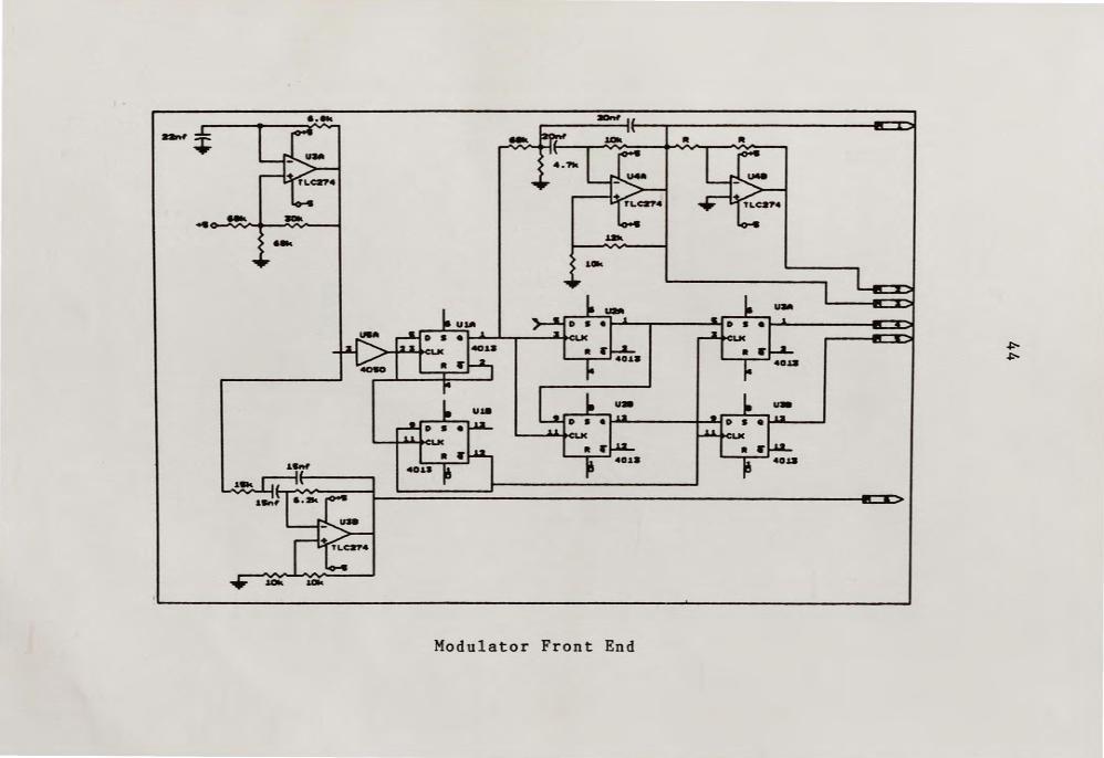
two bits. The block diagram is shown in Figure (3) below.
The actual circuit diagram may be found in the Appendix.
Oscillator at 2400
Frequency Divider
Ser/Par Converter
Bandpass at 1200
Inverter
Allpass = 90
Inverter
L
r
4 - channel Analog Multiplexer
Bandpass ........ ______ _,1
~
at 2400 'Q Figure 3. Modulator Block Diagram.
9

10
The local oscillator output is a 2400 hertz square
wave that provides the timing basis for both the modulator
and demodulatora As mentioned above, this synchronization
between the transmitter and receiver is a prerequisite of
QPSK. There are three common ways of accomplishing it.
The first uses a master timing source to which both the
modulating and demodulating circuitry are directly slaved.
Though very accurate, this method is infeasible when
dealing #ith long distance communication. The second
approach is to transmit a separate pilot signal along with
the information at the expense of increased power and
bandwidth requirements. The pilot signal may be either
frequency or time division multiplexed with the information
carrier, or actually modulated onto that carrier using an
additional modulation scheme. At the receiver, the timing
signal is recovered with its zero crossings used to
generate the local clock. This method is more common in
long distance communication. The third, and probably most
common method is to extract the timing information directly
from the data signal using a variety of methods. This
approach allows the gre~test flexibility of application at
the expense of increased circuit complexity. A good
introduction to these methods can be found in Ziemer and
Tranter (Ziemer and Tranter, 1985). For an in-depth

11
treatment of overall network synchronization, including an
extensive bibliography, see Lindsey et al (Lindsey et al,
1985).
For the present design, the second method is chosen
as a good tradeoff between equipment complexity of the
latter method and the impracticality of the initial one.
As stated above, the coherent detection requirement for
QPSK has already forced a certain degree of complexity.
There is no reason to exacerbate this problem, especially
considering the bandwidth that is available.
To implement this technique in the · circuit, the
buffered output of the 2400 hertz oscillator is input to a
second order bandpass filter tuned to its fundamental
frequency with a bandwidth of approximately 250 hertz.
Ideally, the output of this filter is an inverted sinewave
of the same frequency. If the actual output does not
closely approximate this ideal, that is if the power
spectrum of the clock signal spreads significantly, it
could impair the message signal with which it must be
frequency division multiplexed at the modulator output.
As can be seen from the equation (5) (Stremler, 1982) and
its plot in Figure 4, a 2400 hertz sinusoid would not
interfere with the information signal because it coincides
with a null in the power spectral density of that waveform.
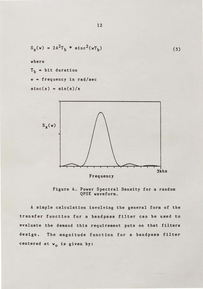
where
Tb= bit duration
w = frequency in rad/sec
sinc(x) = sin(x)/x
12
Frequency
(5)
3khz
Figure 4. Power Spectral Density for a random QPSK waveform.
A simple calculation involving the general form of the
transfer function for a bandpass filter can be used to
evaluate the demand this requirement puts on that filters
design. The magnitude function for a bandpass filter
centered at w0
is given by:

13
I H(w) I = 1 (6)
By taking a ratio of the magnitude squared at three times
the fundamental to that of the fundamental yields the
following approximation for distortion:
D = 1 (7)
1 + (64/9)* Q 2 0
The bandwidth and center frequency listed above result in a
Q0 of approximately 9. 6, yielding well less than one
percent distortion. Therefore, the frequency domain
overlap of the clock and message signals is negligible.
The oscillator output is not only used to generate
the timing signals but also to provide the local carrier
for the modulation process. To accomplish this, the square
wave frequency is divided by a factor of two and tightly
bandpass filtered to extract the fundamental sinusoid.
Distortion, as described above, was again a prime
consideration in determining the bandwidth (i.e. Q) of this
filter. This waveform is then phase shifted by 90 degrees
using a first order all pass filter. Each of these
quadrature signals is then inverted to yield the phase

14
shifts necessary for the QPSK waveform constellation shown
in Figure 5.
x(t) = Acos(wt + k1f/2) k = 0,1,2,3
Figure 5. Phase Constellation for QPSK.
These four waveforms then form four data channels of
an analog multiplexer whose output is directly combined
with the timing sinusoid via a voltage follower amplifier
at the modulator output. This method is chosen in lieu of
a chopper/summer configuration, for example, because of its
simplicity. As mentioned in the introduction, keeping
power to a minimum is one of the goals of this design. To
further that objective, dual polarity power supplies are
used for the active filter operational amplifiers and the
analog multiplexer to avoid transmitting a DC component
that contains no information.
To observe actual circuit operation, a pseudorandom
bit sequence is generated for use as the serial data input.
This data stream is generated using a four bit serial shift
register, cycling back specific outputs through an
exclusive nor gate (XNOR) as the shift register input. A
more detailed look at this circuit may be found in section

15
four where it is described as part of the white noise
simulator. The shift register is clocked at a rate of
1200 hertz to achieve the desired data rate for input into
the dibit serial to parallel converter. Out of this
converter come the inphase (I) and quadrature (Q) data
streams. These channels are fed to the data select inputs
of the multiplexer at 600 baud outputting the information
signal according to Table 1. The oscilloscope trace in the
Appendix serves as a demonstration.
TABLE 1
QUADRATURE DATA TO PHASE CORRELATION
Q I ouq~ut
0 0 + cos(wt)
0 1 + sin(wt)
1 0 - cos(wt)
1 1 - sin(wt)
The final item to discuss pertaining to the
modulator design is the decision not to include a band-
limiting transmission filter at its output. In the ideal,
both transmission and predetection filters would be used to
optimize performance. For this . design however, power
~onsiderations provided an impetus to eliminate one of them

16
on the first iteration. The transmission filter was
omitted because of the better noise rejection provided by
the predetection filter (Jones, 1971).
performance substantiates the decision.
The resulting

SECTION 3
DEMODULATOR DESIGN
The demodulator receives the combined message and
timing signals, as well as any noise acquired enroute. Its
purpose is to coherently demodulate the information,
outputting the inphase and quadrature data streams. These
are then input to a dibit parallel/serial converter that
reproduces the initial data to within a specified error
tolerance. The block diagram is shown on the next page as
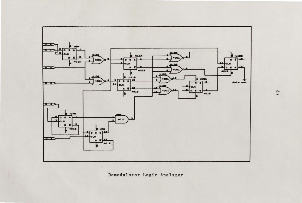
Figure 6. As with the modulator, the actual circuit is
shown in the Appendix.
17

Bandpass at 1200
Bandpass at 2400
Bandreject at 2400
Zero Detector
18
hard limiter
cosine timer
sine timer
cosine integrator
l sine integrator
threshold comparator
decision logic
par/ser converter
Figure 6. Demodulator Block Diagram.
At the demodulator input, the information signal is
separated from the pilot signal by bandpass filters tuned
to the center frequencies of each. The filter that
recovers the timing sinusoid is very similar to the one in
the modulator that originally extracted it from the square
wave. This sinusoid, again inverted by the filter, is
input to a non-inverting zero crossing detector to recreate
that square wave. To minimize the effects of phase jitter,

19
the zero crossing detector is implemented with a Schmitt
trigger. The output then passes through parallel frequency
dividers that trigger on opposite edges of this clock,
yielding quadrature square waves at the desired bit rate.
These square waves control the timing such that the
integration in each channel is synchronized to each of the
quadrature carriers of the modulator. This will be
explained in more detail below.
The predetection filter that extracts the message
from the received signal uses the bandpass filter mentioned
above and a band reject filter centered at the 2400 hertz
of the pilot signal. The use of both filters results from
a tradeoff between out-of-band attenuation and in-band
delay. Specifically, if only the bandpass filter is used,
a large Q or higher order is required to sufficiently
remove the timing signal. The delay distortion resulting
from either case is too great, corrupting the operation of
the data filters that follow. At the other extreme, the
option of using only the band reject filter is denied
because of its lack of noise rejection. As a compromise,
the band reject filter is included to ensure the timing
signal is adequately eliminated and the bandpass filter
bandwidth is extended to reduce the delay distortion. This
can be shown by again calling on the standard form of the
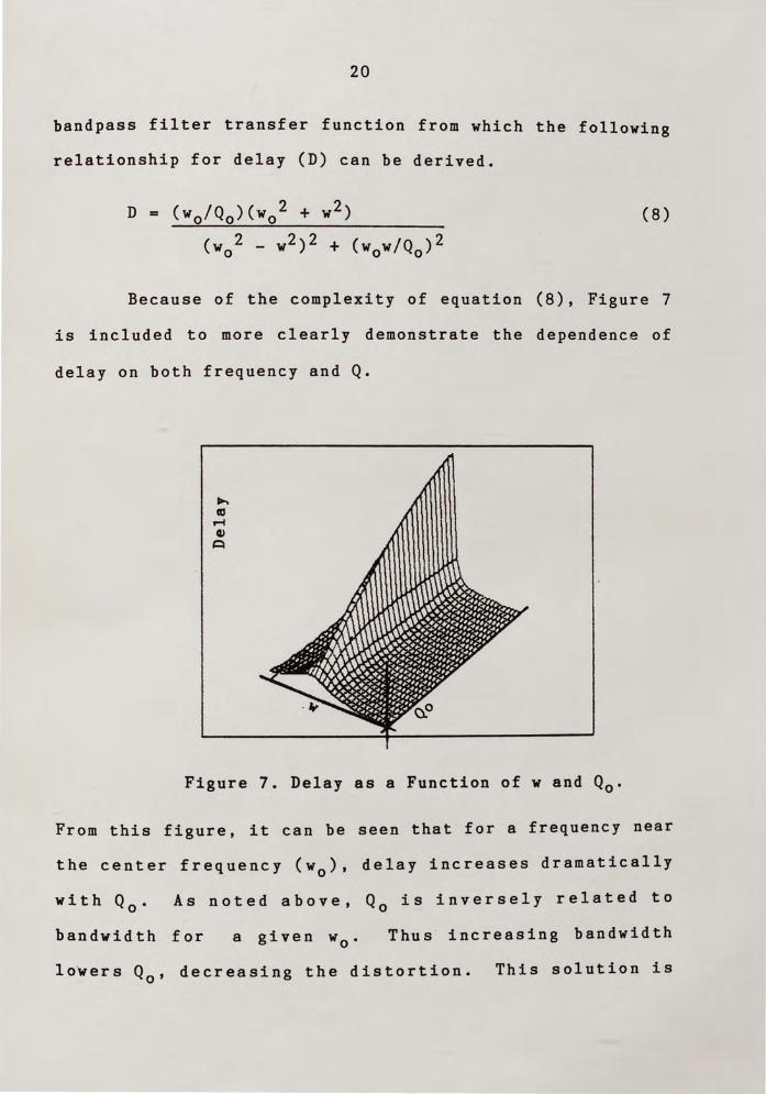
20
bandpass filter transfer function from which the following
relationship for delay (D) can be derived.
D = (wo/Qo)(wo2 + w2) (8)
(w 2 - w2)2 + (w w/Q )2 0 0 0
Because of the complexity of equation (8), Figure 7
is included to more clearly demonstrate the dependence of
delay on both frequency and Q.
Figure 7. Delay as a Function of wand Q0 •
From this figure, it can be seen that for a frequency near
the center frequency (w0
), delay increases dramatically
with Q0
• As noted above, Q0
is inversely related to
bandwidth for Thus · increasing bandwidth
lowers Q0
, decreasing the distortion. This solution is

21
supported by empirical data plotted in Figure 8 (Jones,
1971). Technically this plot pertains to the use of
transmission filters vice the predetection filtering
employed here. However, as stated later in that same work,
both cases respond similarly except for the predetection
filter's better noise rejection.
- INTEGMTE-Atc,.«JUW DETECTION •••• I.JJGL.I 9UTTIIIWOIITM OATA FLTP, It • I
1 -J I --- I I .l---..l·--·-···-• 0.1-N aPPLt OCIYINR TIIANSIIIISIOtl fl. TH
C:: • tAWL• aASEO OIi ._. KLAY I.MAIi PNMEI 0 • W • 11T • IYMIOI. IIIANSlltSSION MTI ~-~-~-~~-~-~--~--~-~~~~~~-~~-~ ...., ~ .
--c,. ~•t---r--tr--T---~--t--~----t-~~~r-""'l~r--~ ... co Q)
Aa~-~-~~-~-~--•--~--~
I t-----+----4~--6---+-~
W/B
Figure 8. Bandwidth Limiting Degradation of QPSK Signals.
The band reject filter's primary function is to
remove the timing signal from the information, yet its
effect on the information itself cannot be ignored.
Ideally this filter would be transparent to the modulated

22
carrier. By tightening the reject band around 2400 hertz,
that ideal can be approached with respect to magnitude,
and only an inversion of phase. Combined with the 180
degree shift of the bandpass filter at its center
frequency, this yields a data signal that is in phase with
the received waveform, and back in phase with the timing
signal which itself is inverted twice, as noted above.
This correction alone does not necessarily eliminate
the errors due to delay distortion. For example, an
earlier design had the carrier frequency equal to the baud
rate, allowing the data filters only one cycle per symbol
over which to operate. Therefore, the significant
attenuation imposed on the higher frequency components of
the symbol boundary transitions masked the phase over a
significant portion of the cycle in which the data filters
were operating. To remedy this, the carrier frequency was
doubled to 1200 hertz and the data filter output was taken
from operations over the second cycle only.
To this point, the discussion has emphasized the
transmitted phase and the distortion of it, as one would
expect. The magnitude of the received signal has not been
discussed for it contains no information. For that reason,
a constant envelope is desired for QPSK. However, when
realistically approaching such a ~esign, the amplitude
di~tortion of the channel and the effect it has on the

23
demodulation process must be considered. For this
application, two methods of offsetting unwanted envelope
fluctuations were pursued. The first was to place an
automatic gain control (AGC) circuit sensitive to full wave
rectified average fluctuations at the front end of the
receiver. The other was to use a hard limiter on the
input. The technique chosen here is the latter for its
simplicity. Realized by a single comparator referenced to
zero, this hard limiter is both simpler and cheaper than
even the more fundamental gain control circuits. As
pointed out by Hanson (Hanson et al, 1984), a strong
argument can be made for the AGC circuit for cases in which
the harmonics generated by the limiting process would
degrade the timing information. For this design though,
the limiting takes place after the clock signal is
extracted, removing the need to sacrifice circuit
simplicity. As a result, the waveform actually processed
by the data filter is not the transmitted sinusoid but a
bipolar square wave that preserves its phase.
The data filters are the central feature of the
demodulator design. Justification for the type chosen here
is best accomplished by briefly digressing to a rather
common discussion of optimum detection in general. Most
introductory texts include this arg~ment in some form. The
development here is effectively a compilation of the more
24
important steps outlined by Carlson (Carlson, 1968) and
Shanmugam (Shanmugam, 1979).
The goal of this development is to derive the
transfer function for the optimum detection filter. The
following notation is added to that already presented:
x(t) = received signal, magnitude of A h(t) = filter impulse response N = average noise power out of the filter y(t) = filter output Gn(f) = n/2 = white noise power spectral density
Starting with the inverse transform of a known
relationship between input and output spectra of a linear
system and taking its magnitude, the following equation may
be written.
I y(t) = I L~(f)X(f)exp(jwt 0 ) df I (9)
= A
The signal to noise ratio (S/N) that is to be maximized is
found by squaring this magnitude and dividing by the
expression for average noise power in terms of its power
spectral density.
A2 = 1Jm:(~)X(f)exp(jwt0 ) df 12 (10)
N Ji H(f) j 2Gn(f) df -a:>
Though the proof is not shown here, ·the Schwarz inequality
can be invoked to simplify this expression. By using this

25
inequality, the numerator is separated into the product of
two integrals.
or
df (11)
Comparing equations (9) and (Jl) along with specializing to
the case of white noise, it can be shown
H(f) = KX*(f)exp(-jwt0
)
(n/2)
(12)
Simplifying by letting K = n/2, the transfer function of
the optimum filter is
H(f) = x*(f)exp(-jwt0
) (13)
Using the shifting and time reversal properties of the
Fourier transform, this can be rewritten as
h(t) = x(t0
- t) (14)

26
This is a rather intriguing result as it states that
the impulse response of the optimum filter has the shape of
the signal itself reversed in time and shifted by some t0
•
For that reason, it is often referred to as a matched
filter. It is interesting to note from equation (11) that
this type of filter can theoretically attain maximum energy
per bit regardless of the signal's shape. Unfortunately,
physical realization of the matched filter is extremely
difficult. To avoid this problem, a correlator
implementation of the matched filter, sometimes called an
integrate and dump filter, is used in this design.
The integrate and dump operation can be derived from
the concept of the matched filter using equation (14) and
the convolution theorem. Letting r(t) represent the
combined information and noise arriving at the receiver, an
expression for the data filter output at t = Tx can be
written
!Tx y(Tx) = r(t)h(Tx - t) dt
-eo (15)
where from equation (14)
h(z) = x(T z) X -
= 0 otherwise

27
Letting z = Tx - t and limiting t to the stated
interval, h(z) can be written as
h(z) = h(Tx - t) = x[Tx - (Tx - t)]
= x(t)
Rewriting equation (15) yields
1Tx r(t)x(t) dt
0
(16)
Therefore it is shown that an alternative to the matched
filter is an integration of the product of the received
signal [r(t)] and a replica of the transmitted carrier
[x(t)]. To more closely approximate the ideal, the
integration is dumped at each Tx interval to zero initial
conditions for subsequent integrations. This avoids a
symbol from affecting adjacent symbols, a phenomenon known
as intersymbol interference. It must be emphasized here
that Tx is not an arbitrary value. It must occur at the
symboling interval to ensure proper, coherent detection.
The data filters used in this demodulator are
integrate and dump type filters, realized by the op-amp
integrator configuration shown on the circuit diagram in
the Appendix. A CMOS switch is paralleled with the
feedback capacitor to discharge it after sampling. Because
of the quadrature nature of the signaling scheme, two

28
separate detection channels are used. As stated above,
timing information is used to synchronize one channel to
the sine wave reference in the modulator, the other to the
cosine. Therefore, for a given phase received, only one of
the channels outputs a non-zero value to the threshold
detectors. This is a direct result of the orthogonality
property of quadrature waveforms.
The primary design consideration for the sample
comparators is at what level to set the threshold (Vth) for
optimality. Because the two channels act independently,
this question can be answered generically for the single
channel case and the result applied to each. This analogy
to a single channel is not absolute however as more logic
is required to decipher the greater number of combinations
outputted by the comparators. Because of the four-level
signaling, each data filter can output one of three
possible values. Applying Rayleigh's theorem to equation
(11), they are:
(17)
where E = signal energy n 0 {t) = filter output noise
The logic guiding the decision process considers two
characteristics of the data filter output. The magnitude
is used to determine which of the q~adrature carriers has

29
been received; the polarity reduces the remaining two
possibilities. For the in-phase (I) channel, the test for
polarity is achieved by using a separate comparator for
each with reference voltage equal to+/- Vth as
appropriate. Each comparator performs the magnitude test
by determining the output between zero and that data
filter's maximum output. Therefore, the magnitude of the
threshold voltage is chosen to optimize this test. Only
the results are summarized here because the actual
derivation of that value involves probability density
expressions that have not been introduced. Using the
probability density functions for the first and third cases
of (17), assuming Gaussian noise distribution and equal
probabilities for one and zero in the input data stream,
the optimum choice for the Vth occurs where the density
functions intersect (Shanmugam, 1979) yielding
Vth = E/2
The value of +/-2 volts used in the present design is
chosen for this reason. Looking at the quadrature channel,
one might notice only one comparator is necessary. Using
the process of elimination for the four possibilities, a
positive determination of the first three implies the
fourth.

30
Having effectively traced the demodulation process
from input to recovered data, all that remains to discuss
is the digital preparation of this data for serial output.
Because the integrations are performed at different times,
a provision must be made to buffer the quadrature channel
before input to the parallel/serial converter. If it is
not done, the clearing of the integrator destroys the data.
This buffering is accomplished by a flip flop on the output
of the lone comparator in that channel. The final stage is
a personal design of a dibit parallel/serial converter to
reform the initial serial data stream.

SECTION 4
AUXILIARY CIRCUITS
The purpose of this section is to briefly describe
the circuits that have been constructed to test the design
presented above. Actually, all three applications are
based on the same circuit, the pseudorandom bit sequence
generator (PRBSG), also called a pseudonoise (PN) sequence
generator. It is constructed using an m-stage serial shift
register in which the input is from the fed back modulo-2
addition of two of the element outputs. This yields a
maximum of 2m - 1 consecutive different states dependent
upon the proper feedback taps. The excluded case is that
of all zeros because it locks up the generator. A listing
of these connections for smaller generators (less than six)
can be found in Ziemer and Tranter (Ziemer and Tranter,
1985).
The reason for the 'pseudorandom' description is
that despite outputting a specific pattern of bits, it
appears random to a third party observer. Mathematically,
this can be shown using the autocorrelation of its output.
Earlier, white noise was assumed to have a power spectral
den~ity function equal to the constant n/2. This implies
31

32
that true white noise has no preferential spectral power
distribution, that is all frequencies have the same power.
The Wiener-Khinchine theorem relates this power spectral
density to the autocorrelation function by proving they
form a Fourier transform pair. The Fourier transform of a
constant yields the Dirac delta function at the origin.
Therefore, for the sequence to appear truly random, its
autocorrelation should approach an impulse. This is indeed
the case. As might be expected, the larger the maximal
length of the sequence, the closer to the ideal it gets.
This can be seen from the plot of this autocorrelation in
terms of m shown in Figure 9.
Figure 9. Pseudorandom Sequence Correlation.

33
The three circuits utilizing the PRBSG are the
initial data source, a white noise simulator and the PRBS
correlator in the demodulator. To serve as the data
source, the PRBSG is clocked at the desired rate bit rate
of 1200 hertz, and its output fed directly to the dibit
serial/parallel converter at the modulator front end. A
seven bit sequence is used for this purpose. How closely
this sequence approximates the ideal can be evaluated using
the chi-square and binomial distributions. The complete
method is outlined in Lane (Lane, 1983). Since QPSK
samples two bits of incoming data at a time to determine
the transmitted symbol, two is chosen as the sample size
required for the calculation. Therefore by comparison with
data tabulated in that paper for a three bit sample of a
seven bit sequence, it can be shown that this sequence is
but a fair approximation of the true randomness. For its
use in the present design though) it is sufficient.
To simulate white noise, the PRBSG is implemented
with an eighteen stage shift register to more closely
represent true randomness. The output of this circuit is
then low pass filtered to remove excessively high frequency
components that would not be present in the channel
considered anyway. Also, since the digital scheme used
everywhere in the design is unipolar NRZ, the output of the
low · pass filter contains an unwanted DC component. This

34
contradicts the zero mean assumed throughout this paper. To
restore that trait, the low pass filter is RC coupled to
the op-amp that sums the noise and the modulator output.
This op-amp configuration also provides the means to change
the noise magnitude relative to that of the signal. This
is necessary for the theory to practice discussion of the
next section. The actual spectrum obtained is shown in the
Appendix.
The PRBS correlator provides the means by which
detection errors are counted. This circuit exploits the
predictability of a pseudorandom sequence generator with
known feedback connections. This is done by using the same
feedback in the receiver PRBSG as that in the transmitter.
Therefore, it is possible to remotely recreate the
pseudorandom sequence serving as the data source in that
transmitter. Unfortunately, being able to reproduce this
sequence is not sufficient to properly ~onitor demodulator
operation. It must also be synchronized to that data.
Using a method taken from Lane (Lane, 1983), this is
accomplished by temporarily opening the correlator feedback
loop and stuffing the shift register with at least enough
received data bits to fill it. Based on a timing circuit
consistent with the bit rate, the feedback loop is then
reinserted and the correlator sequence · is aligned with that
recovered from the channel. These two data streams are

35
then digitally compared by an exclusive or gate. Since
this gate only pulses when the inputs are different, its
output is applied directly to the clock of a counter chip.
The LED's on that chip's output display a binary count of
the error.

SECTION 5
PERFORMANCE ANALYSIS
Conspicuous by its absence in the bulk of the
discussion to this point is the concept of the probability
of error (Pe). Probability of error is the most commonly
used benchmark by which digital systems are judged. Indeed
there are systems in which
like bandwidth or power,
other performance parameters,
supercede its significance.
Generally though, it is one of the more important
considerations of both the designer and the client. The
reason for its absence thus far is that it requires a
completed working system to evaluate it. The previous
sections of this paper have been devoted to that
development. Before focusing on the performance of this
modem specifically, it is necessary to discuss the factors
that determine the probability of error on a theoretical
basis. This is done in the context of an overview of its
derivation.
To allow this development to flow more smoothly,
especially with respect to the notation used, a portion of
the block diagram of a generic QPSK demodulator is shown in
Figure 10.
36

37
Acos(wt)
noise ! n(t) [kTx]
l ('x) {I}"-·~1 y1{t) = x1(t) + n1(t)
correlator 1
--t® Asin(wt) x(t) ! [kTx]
ti f r ~(t) ® = x2(t) + n2(t)
correlator 2
Figure 10. Probability of Error System.
Assuming x(t) = A cos(wct) and noting that the sampling
interval (Tx) is twice the carrier period, it can be shown
YI= A2Tx/2 + n 1(t)
Y2(t) = 0 + nz(t)
If Y1(t) is independent of y 2{t), then errors of the output
of each correlator may be treated likewise.
Provir1g this can be accomplished by demonstrating
the independence of the noise component of the correlator
outputs. Since these noise outputs are both uncorrelated
and Gaussian, they are independent. The ref ore, y1 ( t) and
y 2{t). are independent. It can be also shown the variances
of these outputs are equal to

38
Determining the probability of error for the phase-matched
channel amounts to evaluating the possibility of the noise
actually offsetting the signal at the correlator output,
that is
which can be shown to equal
Therefore the probability of the correct output is 1-Pel·
The fact that these probabilities are independent is now
used to write the probability that both channels are
correct.
P = (1-P 1 )(1-P 2) c e e
Finally, assuming Pel<< 1, the final form is written
This is consistent with the ideal relationship plotted in
Figure 1. Table 2 shows a sample of the actual performance
of this design. It falls significantly short of the ideal
calculations presented above.

39
TABLE 2
ACTUAL PROBABILITY OF ERROR PERFORMANCE
S/N (db)
21.1
18.0
15.0
Pe
212.7e-6
230.8e-6
2.4e-3
A survey of the literature pertinent to the
specifications of this design uncovers a method of possibly
improving the performance listed above. Though it involves
changing the integrate and dump data filters, it is not
contradictory to the detection optimization derived above.
It is shown that passive data filters often outperform
matched filters when there exists a significant amount of
channel and demodulator distortion (Jones, 1971 and Austin
et al, 1983). The reconciliation between this and the
optimum detection proof lies in the fact that the heavily
distorted signal no longer satisfies equation (15). Though
the impulse response of the data filter does not change, it
is no longer a time reversed and shifted version of the
received signal.
distorted signal.
That is, it is no longer matched to the
The present design remains intact
because the magnitude of the improvement, as seen in Figure
8, does not warrant the change.

40
Another improvement would be to increase the pilot
signal frequency relative to the carrier frequency. This
would allow even less restrictive band-limiting at the
demodulator input, further decreasing the demodulator
distortion described in Section 3.

SECTION 6
CONCLUSION
Quadrature phase shift key modulation can find
useful application for data transmission over a standard
telephone line. The design described in this paper is a
fundamental example. Presently, in the literature, there
are numerous designs that more fully exploit the advantages
of the phase shift key technique. This is especially
important in light of the growing demand for increased data
transmission rates. When paying for the use of the
transmission channel, speed translates into reduced costs
for the consumer. In addition, with continued advancement
in the field of application specific integrated circuits,
the complexity that once escalated production costs is no
longer of major concern.
In the future, digital communications in general
will continue to flourish. Single chip, fully implemented
modems are indicative of the hardware improvements that
have taken place in recent years. Highly efficient coding
techniques represent both software and hardware
advancement. This trend should continue considering the
vast amount of research presently being done in the field.
41

42
In addition, if proposed standards presently being
considered are adopted, they could provide a common
foundation on which to build.

APPENDIX A
MODULATOR AND DEMODULATOR SCHEMATICS
43
44
• ",:j
.. !
I. D
~
.. ..
~
+l ~
0 M
~
M
0 +
l a,
r-f ::s
",:j
0 ,::
'

w=I>---~-..r-=--=--=--=--=--=--=--=--=--=--=--=--=--=--=--:..--1 u•
40U
1Clk
.. tel.-.._,. c:hawlel
&Ok
Modulator Output
.i:::,. VI
47
r----,i • I ~
Ill 5.
1-4·
0 .µ
t't1
r-f :,
't:i 0 e Q
)
A

APPENDIX B
WAVEFORM PLOTS
48

49
QPSK Oscilloscope Trace

50
Noise Spectral Plot

LIST OF REFERENCES
Anderson, John B., Aulin, Tor, Sundberg, Carl-Erik, Digital Phase Modulation. New York: Plenum Press, 1986
Austin, Mark C., Chang, Ming U., Horwood, Daniel F., and Maslov, Robert A. "QPSK, Staggered QPSK, and MSK-A Comparative Evaluation." IEEE Transactions on Communications 31 (February 1983): 171-182.
Carlson, A. Bruce, Communication Systems. New .York: McGrawHill Book Co mpany, 1968
Daryanani, Gobind. Principles of Active Network Svnthesis and Design. New York: John Wiley and Sons, 1976.
Hanson, Kerry, Severin, William A., Klinkovsky, Edward R., Richardson, Donald C., Hochschild, James R. "1200 Bit/s QPSK Full Duplex Modem." IEEE Journal of Solid-State Circuits 19 (December 1984): 878-887.
Jones, J. Jay. "Filter Distortion and Intersymbol Interference Effects on PSK Signals." IEEE Tr4nsactions on Communications. Technology 19 (April 1971): 120-132.
Lane, Barry. "Digital Communications System Evaluation: Design Developments in Pseudorandom Sequence Usage, Signal Conditioning and Timing Regeneration." Master's Thesis, University of Central Florida, 1983.
Lindsey, William C., Ghazvinian, Farzad, Hagmann, Walter C., Dessouky, Khaled, "Network Synchronization." Proceedings of the IEEE 73 (October 1985): 1445-1466.
Schwartz, Mischa. Information Transmission, Modulation and Noise. New York: McGraw Hill, 1980.
Shanmugam, K. Sam. Digital and Analog Communication Systems. New York: John Wiley and Sons, 1979.
Stremler, Ferrel G. Introduction to Communication Systems. Massachusetts: Addison-Wesley, 1982.
51

52
Ziemer, R. E., and Tranter, W. H. Principles of Communication Systems, Modulation and Noise. Boston: Houghton Mifflin, 1985. · <