department of electronics and communication … list of experiments sl no experiments page no 1...
TRANSCRIPT

1
Department of Electronics and Communication Engineering
Sub Code/Name: BEC3L2- DIGITAL ELECTRONICS LAB
Name : ……………………………………
Reg No : ……………………………………
Branch : ……………………………………
Year & Semester : ……………………………………

2
LIST OF EXPERIMENTS
Sl No Experiments Page No
1 Study of logic gates 4
2 Design and implementation of adders and subtractors using logic gates 9
3 Design and implementation of encoder and decoder using logic gates. 15
4 Design and implementation of multiplexer and demultiplexer using logic gates. 20
5 Design and implementation of 2-bit magnitude comparator using logic gates, 28
6 Design and implementation of 16-bit odd/even parity checker. 32
7 Design and implementation of Flipflops using logic gates. 36
8 Design and implementation of code converters using logic gates. 40
9 Design and implementation of counters. 56
10 Design and Implementation of shift registers 67

3
INDEX
Expt. Expt. Name of the Experiment Marks Staff SIGN
\

4
STUDY OF LOGIC GATES
Ex No:1
Date:
Aim: To study and verify the Truth Tables of AND, OR, NOT, NAND, NOR EXOR logic gates for positive logic.
Objective:
To get familiar with the usage of the available lab equipments. To get familiar with Prototyping board (breadboard) To describe and verify the operation for the AND, OR, NOT, NAND, NOR,
XOR gates. To study the representation of these functions by truth tables, logic diagrams
and Boolean algebra To Introduce a basic knowledge in integrated circuit devices operation To practice how to build a simple digital circuit using ICs and other digital
components . Learn how to Wire a circuit
Appararus/ Equipment Required:
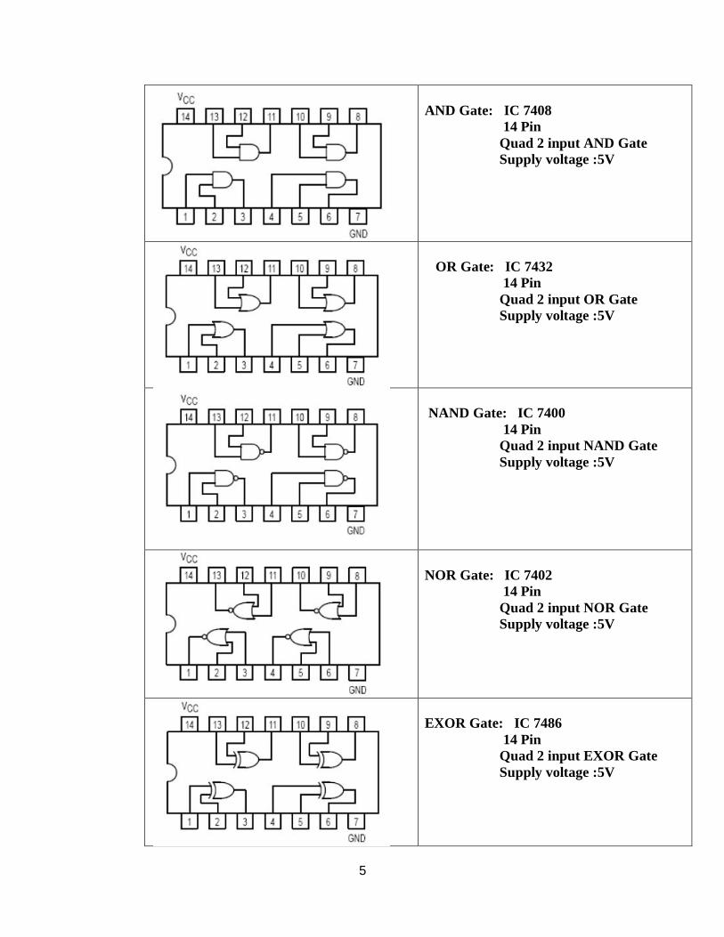
Digital ICs: 7404 :Hex Inverter 7408 :Quad 2 input AND 7432 :Quad 2 input OR 7400: Quad 2 input NAND 7402: Quad 2 inpu 7486: Quad 2 input EXOR
Trainer kit Connecting Wires
Pin Diagram:
Not Gate: IC 7404(HEX Inverter) 14 Pin Supply voltage :5V
5
AND Gate: IC 7408 14 Pin Quad 2 input AND Gate Supply voltage :5V
OR Gate: IC 7432 14 Pin Quad 2 input OR Gate Supply voltage :5V
NAND Gate: IC 7400 14 Pin Quad 2 input NAND Gate Supply voltage :5V
NOR Gate: IC 7402 14 Pin Quad 2 input NOR Gate Supply voltage :5V
EXOR Gate: IC 7486 14 Pin Quad 2 input EXOR Gate Supply voltage :5V
6
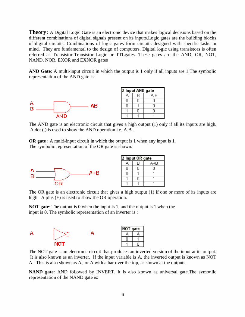
Theory: A Digital Logic Gate is an electronic device that makes logical decisions based on the different combinations of digital signals present on its inputs.Logic gates are the building blocks of digital circuits. Combinations of logic gates form circuits designed with specific tasks in mind. They are fundamental to the design of computers. Digital logic using transistors is often referred as Transistor-Transistor Logic or TTLgates. These gates are the AND, OR, NOT, NAND, NOR, EXOR and EXNOR gates
AND Gate: A multi-input circuit in which the output is 1 only if all inputs are 1.The symbolic representation of the AND gate is:
The AND gate is an electronic circuit that gives a high output (1) only if all its inputs are high. A dot (.) is used to show the AND operation i.e. A.B . OR gate : A multi-input circuit in which the output is 1 when any input is 1. The symbolic representation of the OR gate is shown:
The OR gate is an electronic circuit that gives a high output (1) if one or more of its inputs are high. A plus (+) is used to show the OR operation. NOT gate: The output is 0 when the input is 1, and the output is 1 when the input is 0. The symbolic representation of an inverter is :
The NOT gate is an electronic circuit that produces an inverted version of the input at its output. It is also known as an inverter. If the input variable is A, the inverted output is known as NOT A. This is also shown as A', or A with a bar over the top, as shown at the outputs. NAND gate: AND followed by INVERT. It is also known as universal gate.The symbolic representation of the NAND gate is:
7
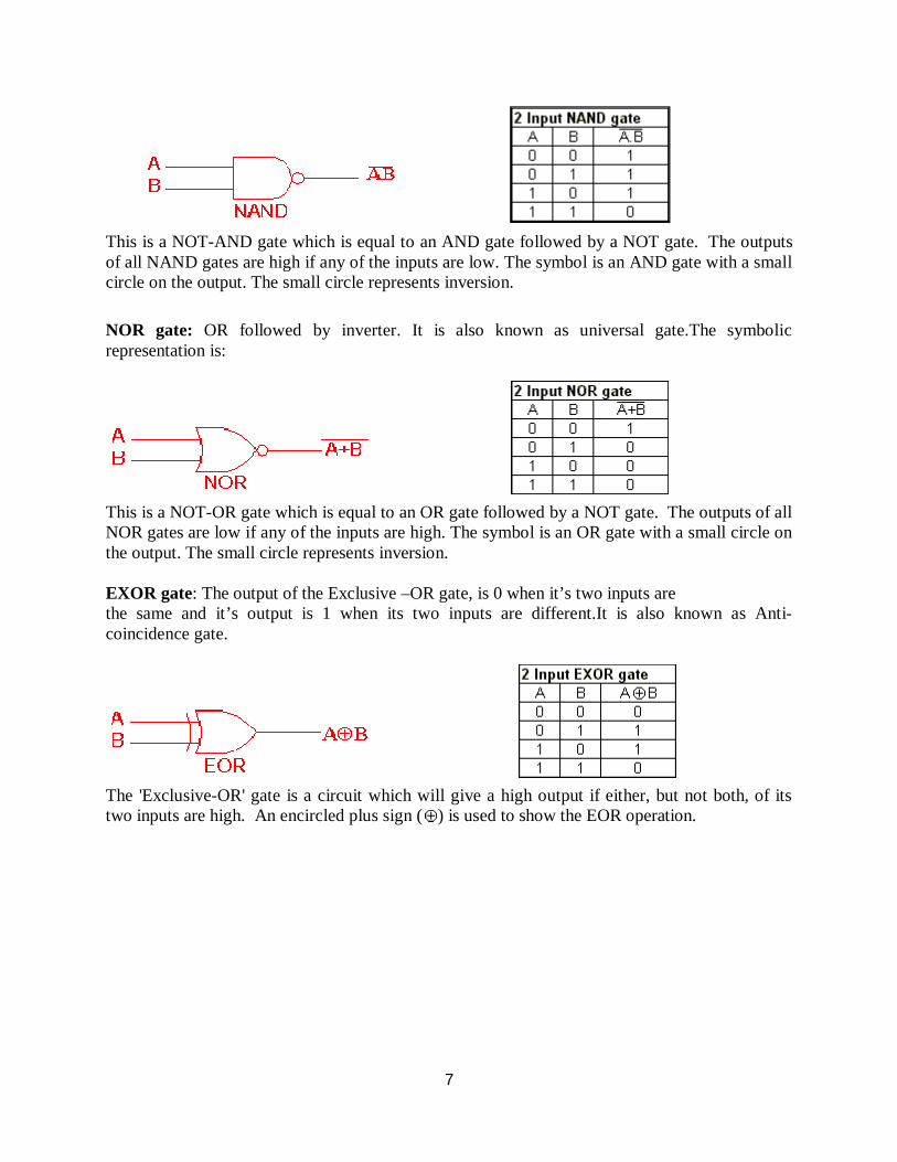
This is a NOT-AND gate which is equal to an AND gate followed by a NOT gate. The outputs of all NAND gates are high if any of the inputs are low. The symbol is an AND gate with a small circle on the output. The small circle represents inversion.
NOR gate: OR followed by inverter. It is also known as universal gate.The symbolic representation is:
This is a NOT-OR gate which is equal to an OR gate followed by a NOT gate. The outputs of all NOR gates are low if any of the inputs are high. The symbol is an OR gate with a small circle on the output. The small circle represents inversion.
EXOR gate: The output of the Exclusive –OR gate, is 0 when it’s two inputs are the same and it’s output is 1 when its two inputs are different.It is also known as Anti-coincidence gate.
The 'Exclusive-OR' gate is a circuit which will give a high output if either, but not both, of its two inputs are high. An encircled plus sign ( ) is used to show the EOR operation.
8
Procedure:
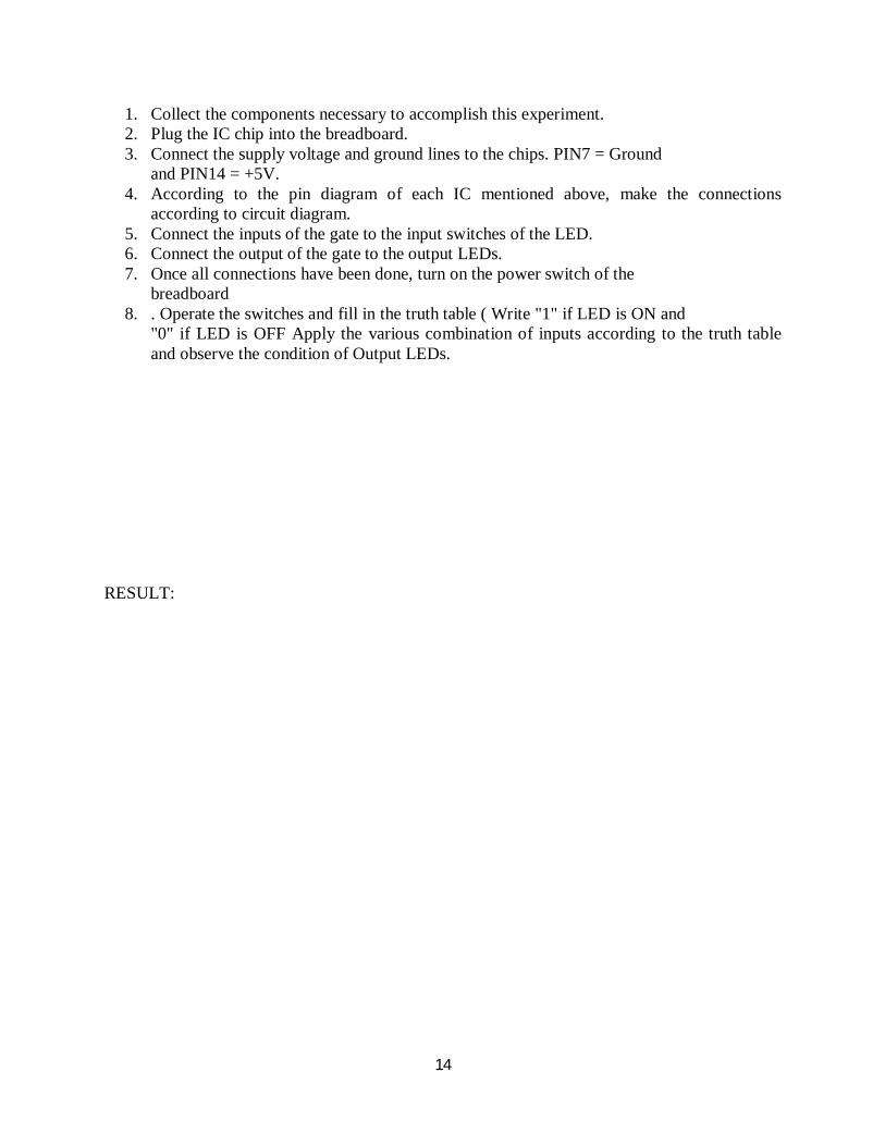
1. Collect the components necessary to accomplish this experiment. 2. Plug the IC chip into the breadboard.
3. Connect the supply voltage and ground lines to the chips. PIN7 = Ground
and PIN14 = +5V.
4. According to the pin diagram of each IC mentioned above, wire only one
gate to verify its truth table.
5. Connect the inputs of the gate to the input switches of the LED.
6. Connect the output of the gate to the output LEDs.
7. Once all connections have been done, turn on the power switch of the
breadboard
8. . Operate the switches and fill in the truth table ( Write "1" if LED is ON and
"0" if LED is OFF Apply the various combination of inputs according to the truth table
and observe the condition of Output LEDs.
9. Repeat the above steps 1 to 5 for all the ICs.
\
RESULT:

9
Ex No:2
Date:
DESIGN AND IMPLEMENTATION OF ADDERS AND SUBTRACTORS USING LOGIC GATES
Aim: Design and verify the logic circuit of Half adder using logic gates. Design and verify the logic circuit Full adder using of Half adder. Design and verify the logic circuit of Half subtractor using logic gates. Design and verify the logic circuit Full subtractor using of Half subtractor. Objective:
a. To understand the principle of binary addition. b. To understand and to differentiate half & full adder concept. c. Use truth table, Karnaugh map, and Boolean Algebra theorems in simplifying a circuit design. d. To implement half adder and full adder circuit uing logic gates
Apparatus Required: Trainer kit Digital ICs: 7408 :Quad 2 input AND
7486: Quad 2 input EXOR 7432 :Quad 2 input OR
Connecting Wires Pin Diagram: Half Adder:
Fig 2.1: Pin Diagram Of Half Adder
10
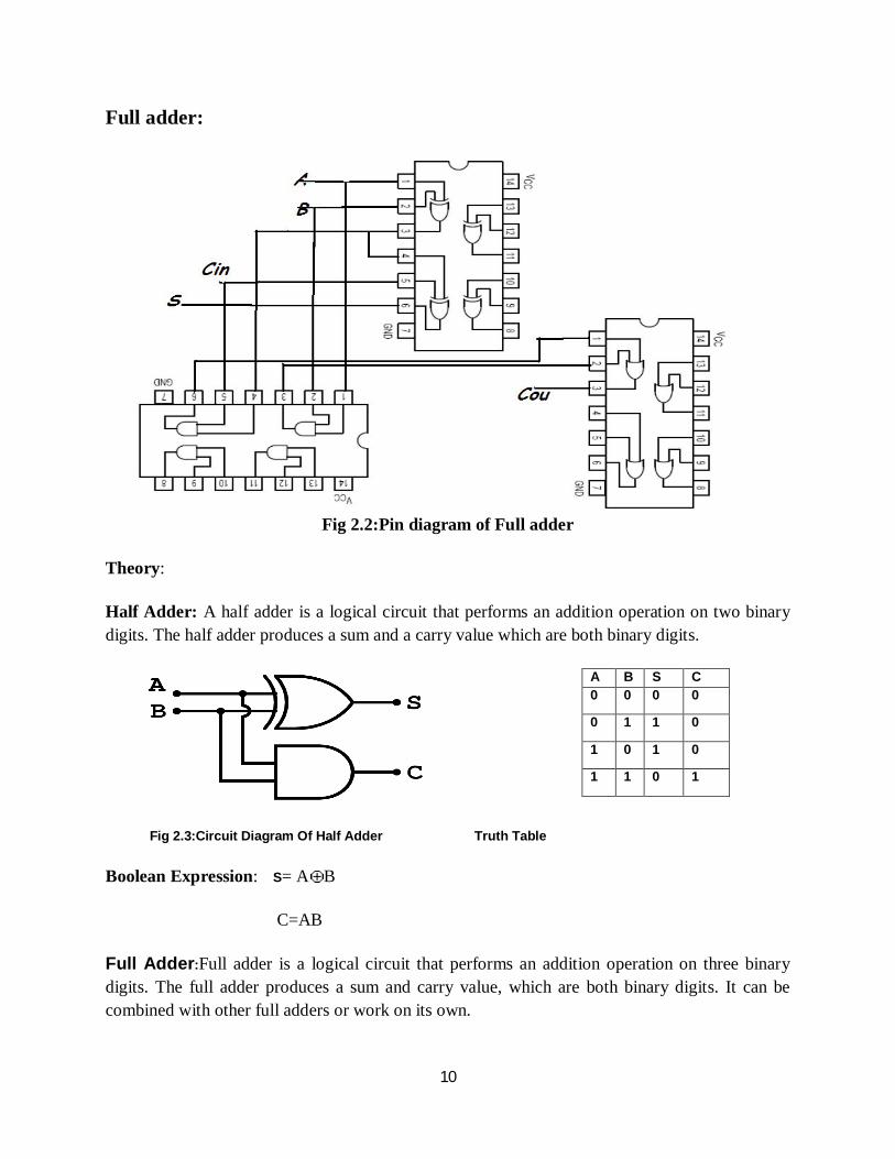
Full adder:
Fig 2.2:Pin diagram of Full adder
Theory:
Half Adder: A half adder is a logical circuit that performs an addition operation on two binary digits. The half adder produces a sum and a carry value which are both binary digits.
A B S C 0 0 0 0
0 1 1 0
1 0 1 0
1 1 0 1
Fig 2.3:Circuit Diagram Of Half Adder Truth Table
Boolean Expression: S= A B
C=AB
Full Adder:Full adder is a logical circuit that performs an addition operation on three binary digits. The full adder produces a sum and carry value, which are both binary digits. It can be combined with other full adders or work on its own.
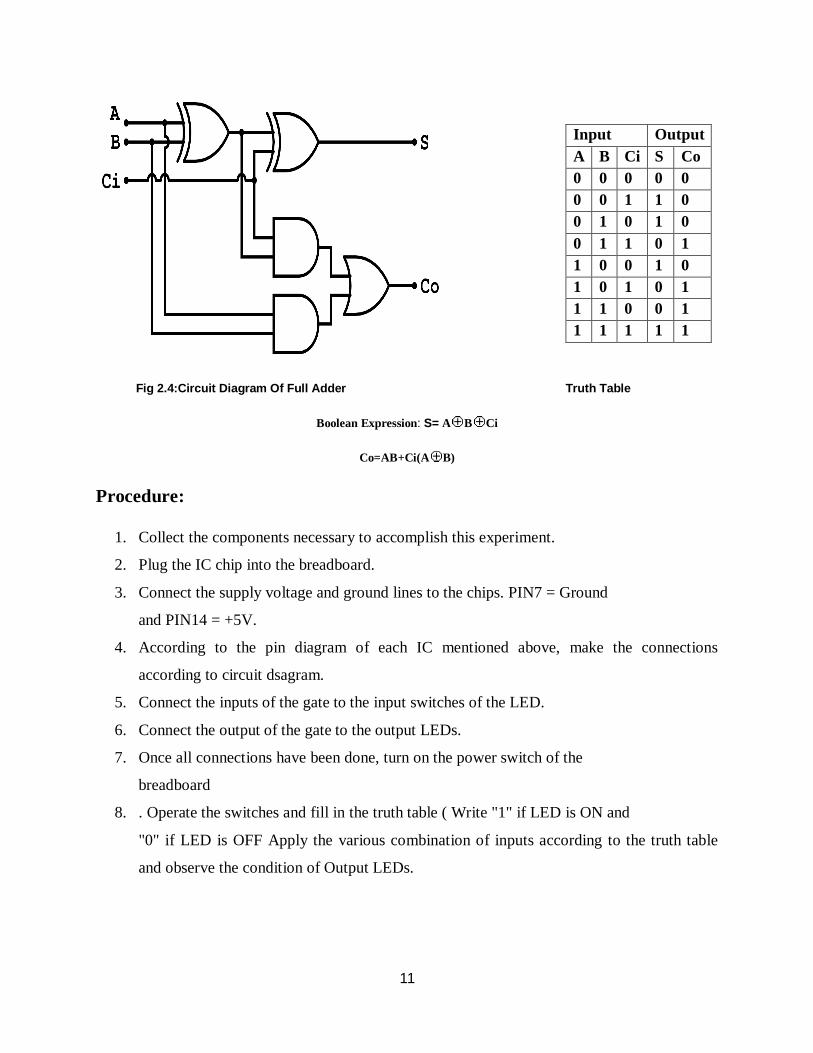
11
Input Output A B Ci S Co 0 0 0 0 0 0 0 1 1 0 0 1 0 1 0 0 1 1 0 1 1 0 0 1 0 1 0 1 0 1 1 1 0 0 1 1 1 1 1 1
Fig 2.4:Circuit Diagram Of Full Adder Truth Table
Boolean Expression: S= A B Ci
Co=AB+Ci(A B)
Procedure:
1. Collect the components necessary to accomplish this experiment.
2. Plug the IC chip into the breadboard.
3. Connect the supply voltage and ground lines to the chips. PIN7 = Ground
and PIN14 = +5V.
4. According to the pin diagram of each IC mentioned above, make the connections
according to circuit dsagram.
5. Connect the inputs of the gate to the input switches of the LED.
6. Connect the output of the gate to the output LEDs.
7. Once all connections have been done, turn on the power switch of the
breadboard
8. . Operate the switches and fill in the truth table ( Write "1" if LED is ON and
"0" if LED is OFF Apply the various combination of inputs according to the truth table
and observe the condition of Output LEDs.
12
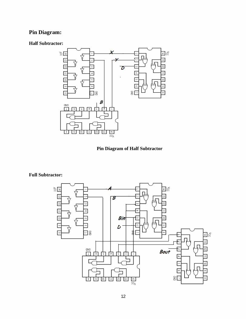
Pin Diagram:
Half Subtractor:
Pin Diagram of Half Subtractor
Full Subtractor:
13
Pin Diagram of Full subtarctor
Theory :
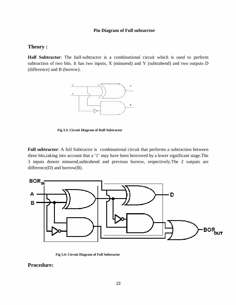
Half Subtractor: The half-subtractor is a combinational circuit which is used to perform subtraction of two bits. It has two inputs, X (minuend) and Y (subtrahend) and two outputs D (difference) and B (borrow).
Fig 3.3: Circuit Diagram of Half Subtractor
Full subtractor: A full Subtractor is combinational circuit that performs a subtraction between three bits,taking into account that a ‘1’ may have been borrowed by a lower significant stage.The 3 inputs denote minuend,subtrahend and previous borrow, respectively.The 2 outputs are difference(D) and borrow(B).
Fig 3.4: Circuit Diagram of Full Subtractor
Procedure:
14
1. Collect the components necessary to accomplish this experiment. 2. Plug the IC chip into the breadboard. 3. Connect the supply voltage and ground lines to the chips. PIN7 = Ground
and PIN14 = +5V. 4. According to the pin diagram of each IC mentioned above, make the connections
according to circuit diagram. 5. Connect the inputs of the gate to the input switches of the LED. 6. Connect the output of the gate to the output LEDs. 7. Once all connections have been done, turn on the power switch of the
breadboard 8. . Operate the switches and fill in the truth table ( Write "1" if LED is ON and
"0" if LED is OFF Apply the various combination of inputs according to the truth table and observe the condition of Output LEDs.
RESULT:
15
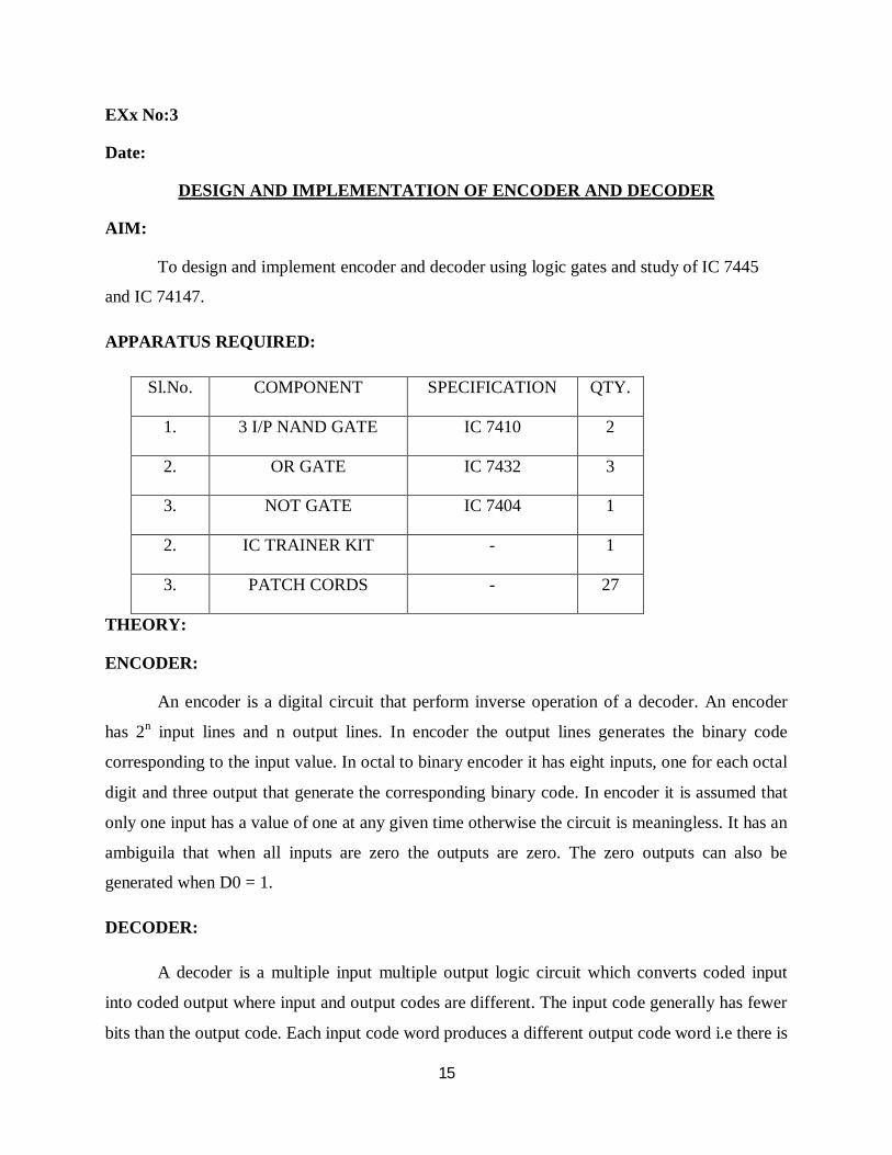
EXx No:3
Date:
DESIGN AND IMPLEMENTATION OF ENCODER AND DECODER
AIM:
To design and implement encoder and decoder using logic gates and study of IC 7445
and IC 74147.
APPARATUS REQUIRED:
Sl.No. COMPONENT SPECIFICATION QTY.
1. 3 I/P NAND GATE IC 7410 2
2. OR GATE IC 7432 3
3. NOT GATE IC 7404 1
2. IC TRAINER KIT - 1
3. PATCH CORDS - 27
THEORY:
ENCODER:
An encoder is a digital circuit that perform inverse operation of a decoder. An encoder
has 2n input lines and n output lines. In encoder the output lines generates the binary code
corresponding to the input value. In octal to binary encoder it has eight inputs, one for each octal
digit and three output that generate the corresponding binary code. In encoder it is assumed that
only one input has a value of one at any given time otherwise the circuit is meaningless. It has an
ambiguila that when all inputs are zero the outputs are zero. The zero outputs can also be
generated when D0 = 1.
DECODER:
A decoder is a multiple input multiple output logic circuit which converts coded input
into coded output where input and output codes are different. The input code generally has fewer
bits than the output code. Each input code word produces a different output code word i.e there is
16
one to one mapping can be expressed in truth table. In the block diagram of decoder circuit the
encoded information is present as n input producing 2n possible outputs. 2n output values are
from 0 through out 2n – 1.
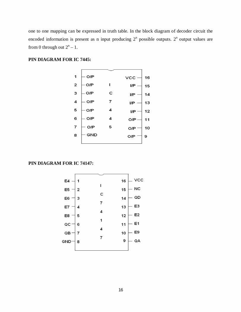
PIN DIAGRAM FOR IC 7445:
PIN DIAGRAM FOR IC 74147:
17
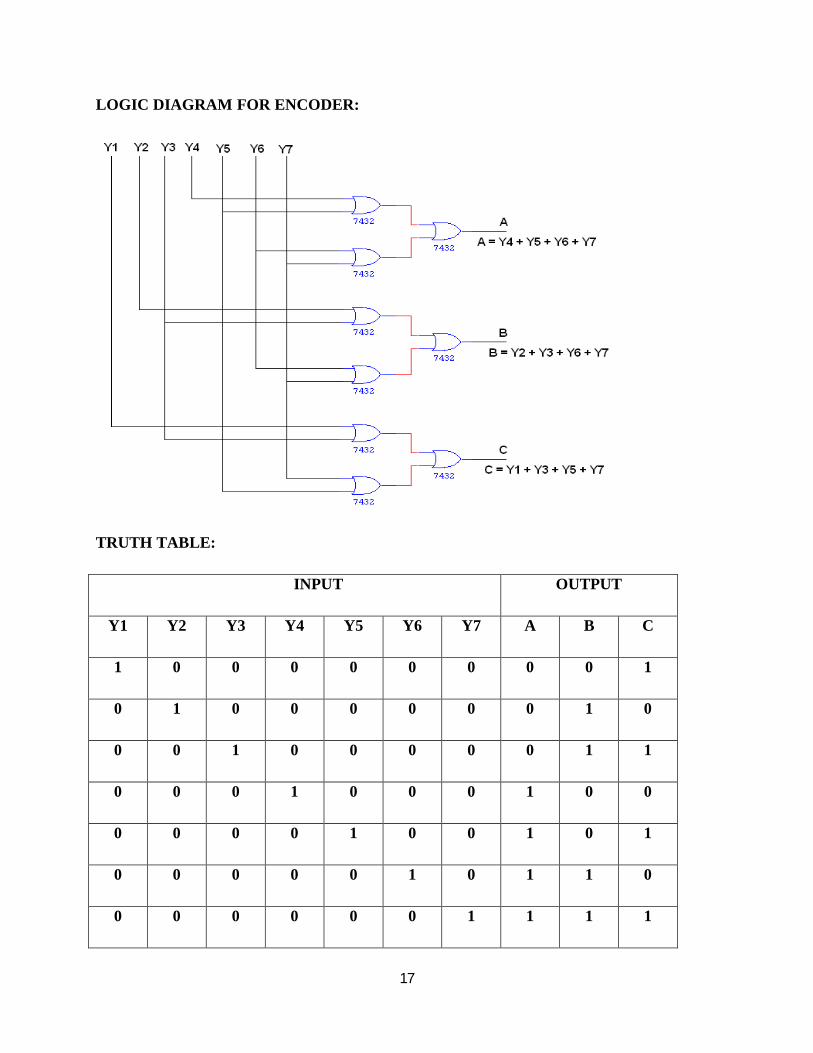
LOGIC DIAGRAM FOR ENCODER:
TRUTH TABLE:
INPUT OUTPUT
Y1 Y2 Y3 Y4 Y5 Y6 Y7 A B C
1 0 0 0 0 0 0 0 0 1
0 1 0 0 0 0 0 0 1 0
0 0 1 0 0 0 0 0 1 1
0 0 0 1 0 0 0 1 0 0
0 0 0 0 1 0 0 1 0 1
0 0 0 0 0 1 0 1 1 0
0 0 0 0 0 0 1 1 1 1
18
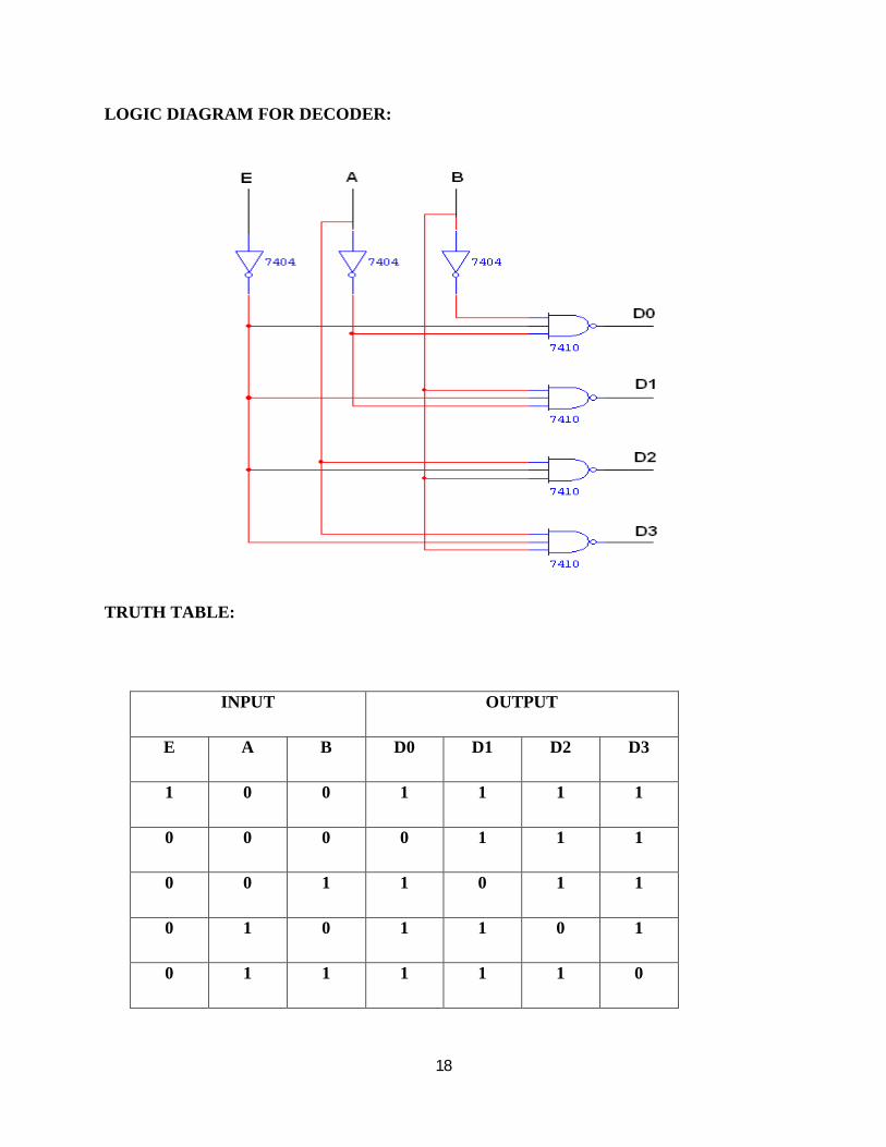
LOGIC DIAGRAM FOR DECODER:
TRUTH TABLE:
INPUT OUTPUT
E A B D0 D1 D2 D3
1 0 0 1 1 1 1
0 0 0 0 1 1 1
0 0 1 1 0 1 1
0 1 0 1 1 0 1
0 1 1 1 1 1 0

19
PROCEDURE:
(i) Connections are given as per circuit diagram.
(ii) Logical inputs are given as per circuit diagram.
(iii) Observe the output and verify the truth table.
RESULT:
20
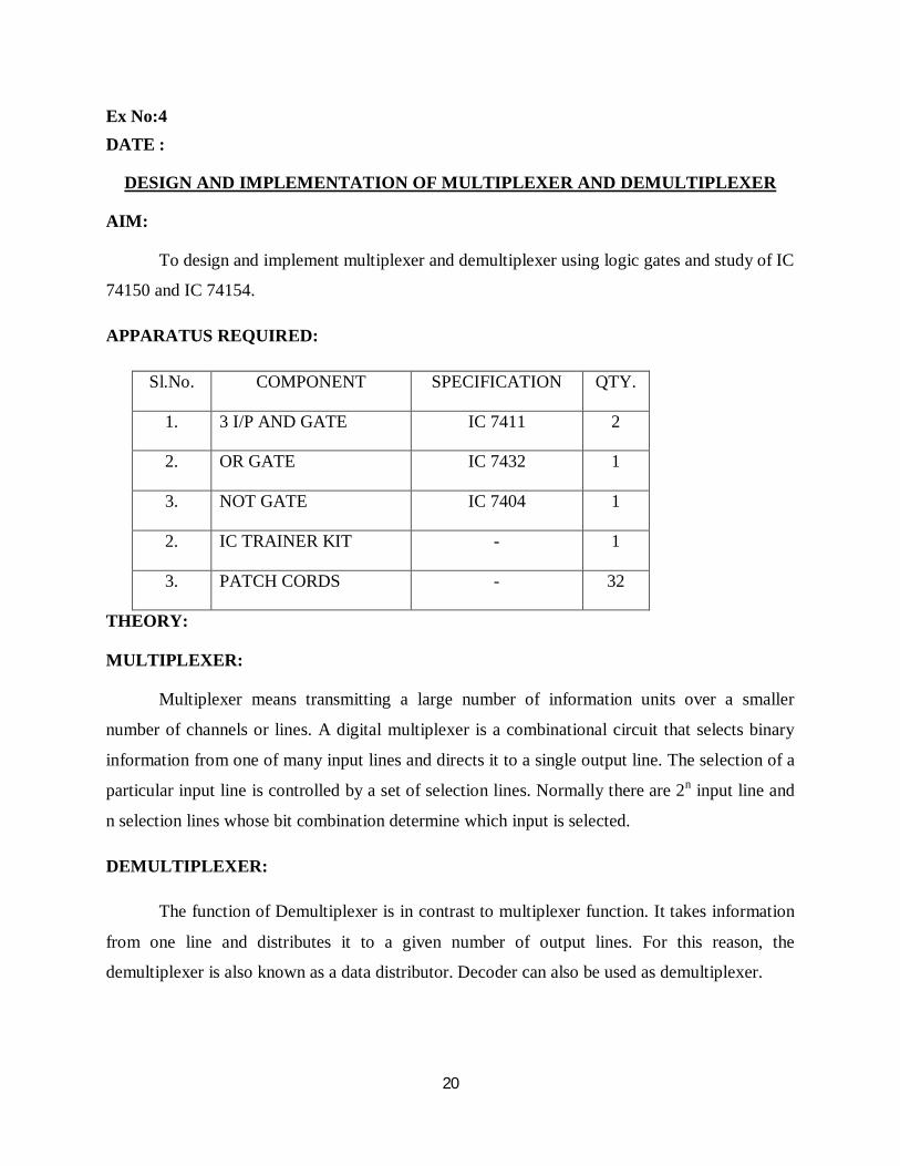
Ex No:4 DATE :
DESIGN AND IMPLEMENTATION OF MULTIPLEXER AND DEMULTIPLEXER
AIM:
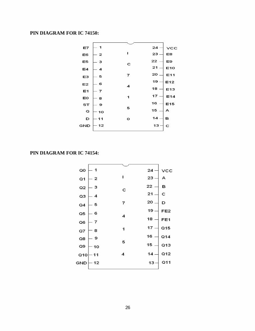
To design and implement multiplexer and demultiplexer using logic gates and study of IC
74150 and IC 74154.
APPARATUS REQUIRED:
Sl.No. COMPONENT SPECIFICATION QTY.
1. 3 I/P AND GATE IC 7411 2
2. OR GATE IC 7432 1
3. NOT GATE IC 7404 1
2. IC TRAINER KIT - 1
3. PATCH CORDS - 32
THEORY:
MULTIPLEXER:
Multiplexer means transmitting a large number of information units over a smaller
number of channels or lines. A digital multiplexer is a combinational circuit that selects binary
information from one of many input lines and directs it to a single output line. The selection of a
particular input line is controlled by a set of selection lines. Normally there are 2n input line and
n selection lines whose bit combination determine which input is selected.
DEMULTIPLEXER:
The function of Demultiplexer is in contrast to multiplexer function. It takes information
from one line and distributes it to a given number of output lines. For this reason, the
demultiplexer is also known as a data distributor. Decoder can also be used as demultiplexer.
21
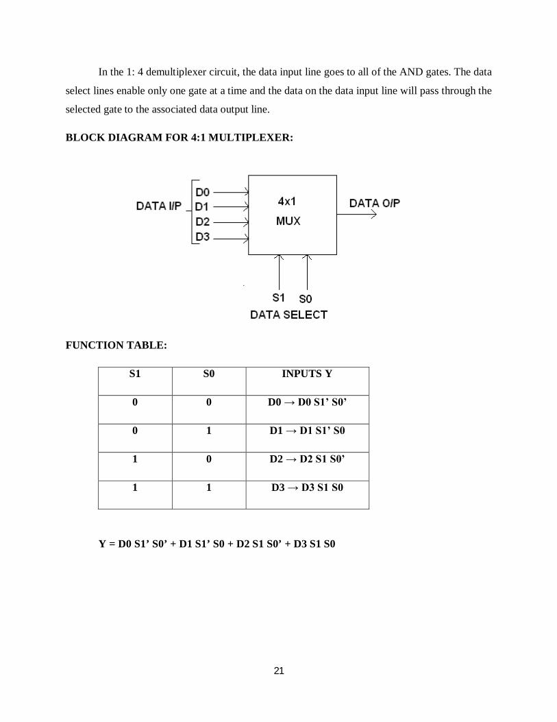
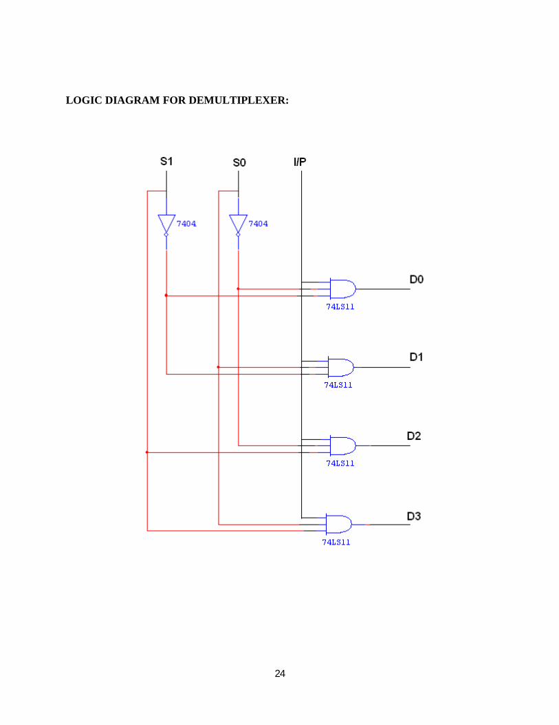
In the 1: 4 demultiplexer circuit, the data input line goes to all of the AND gates. The data
select lines enable only one gate at a time and the data on the data input line will pass through the
selected gate to the associated data output line.
BLOCK DIAGRAM FOR 4:1 MULTIPLEXER:
FUNCTION TABLE:
S1 S0 INPUTS Y
0 0 D0 → D0 S1’ S0’
0 1 D1 → D1 S1’ S0
1 0 D2 → D2 S1 S0’
1 1 D3 → D3 S1 S0
Y = D0 S1’ S0’ + D1 S1’ S0 + D2 S1 S0’ + D3 S1 S0
22
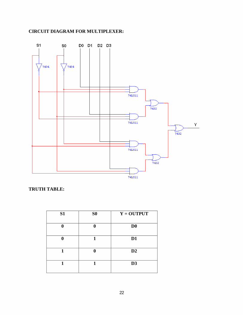
CIRCUIT DIAGRAM FOR MULTIPLEXER:
TRUTH TABLE:
S1 S0 Y = OUTPUT
0 0 D0
0 1 D1
1 0 D2
1 1 D3
23
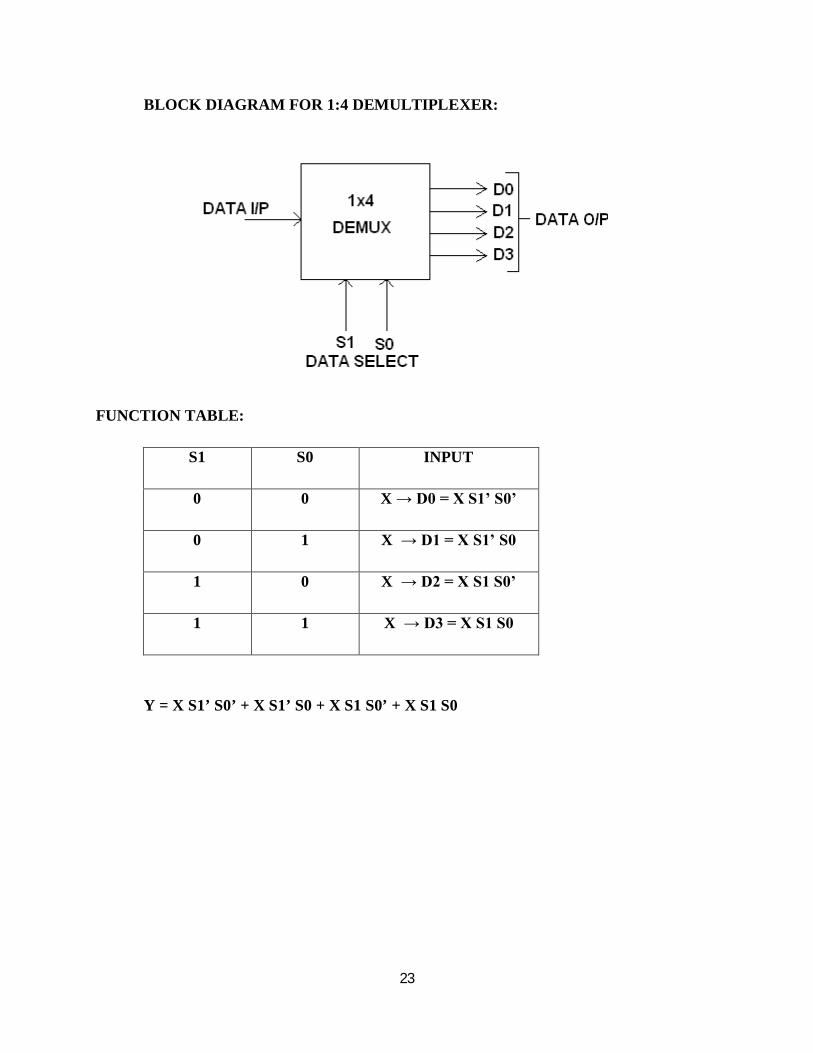
BLOCK DIAGRAM FOR 1:4 DEMULTIPLEXER:
FUNCTION TABLE:
S1 S0 INPUT
0 0 X → D0 = X S1’ S0’
0 1 X → D1 = X S1’ S0
1 0 X → D2 = X S1 S0’
1 1 X → D3 = X S1 S0
Y = X S1’ S0’ + X S1’ S0 + X S1 S0’ + X S1 S0
24
LOGIC DIAGRAM FOR DEMULTIPLEXER:
25
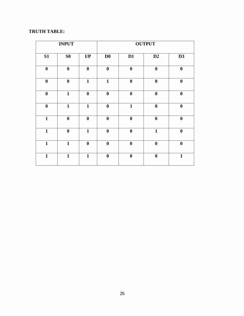
TRUTH TABLE:
INPUT OUTPUT
S1 S0 I/P D0 D1 D2 D3
0 0 0 0 0 0 0
0 0 1 1 0 0 0
0 1 0 0 0 0 0
0 1 1 0 1 0 0
1 0 0 0 0 0 0
1 0 1 0 0 1 0
1 1 0 0 0 0 0
1 1 1 0 0 0 1
26
PIN DIAGRAM FOR IC 74150:
PIN DIAGRAM FOR IC 74154:

27
PROCEDURE:
(i) Connections are given as per circuit diagram.
(ii) Logical inputs are given as per circuit diagram.
(iii) Observe the output and verify the truth table.
RESULT:

28
Ex No:5 DATE :
DESIGN AND IMPLEMENTATION OF MAGNITUDE COMPARATOR AIM:
To design and implement 2 – bit magnitude comparator using basic gates.
APPARATUS REQUIRED:
Sl.No.
COMPONENT SPECIFICATION QTY.
1. AND GATE IC 7408 2
2. X-OR GATE IC 7486 1
3. OR GATE IC 7432 1
4. NOT GATE IC 7404 1
5. 4-BIT MAGNITUDE COMPARATOR
IC 7485 2
6. IC TRAINER KIT - 1
7. PATCH CORDS - 30
THEORY:
The comparison of two numbers is an operator that determine one number is greater than,
less than (or) equal to the other number. A magnitude comparator is a combinational circuit that
compares two numbers A and B and determine their relative magnitude. The outcome of the
comparator is specified by three binary variables that indicate whether A>B, A=B (or) A<B.
A = A3 A2 A1 A0
B = B3 B2 B1 B0
29
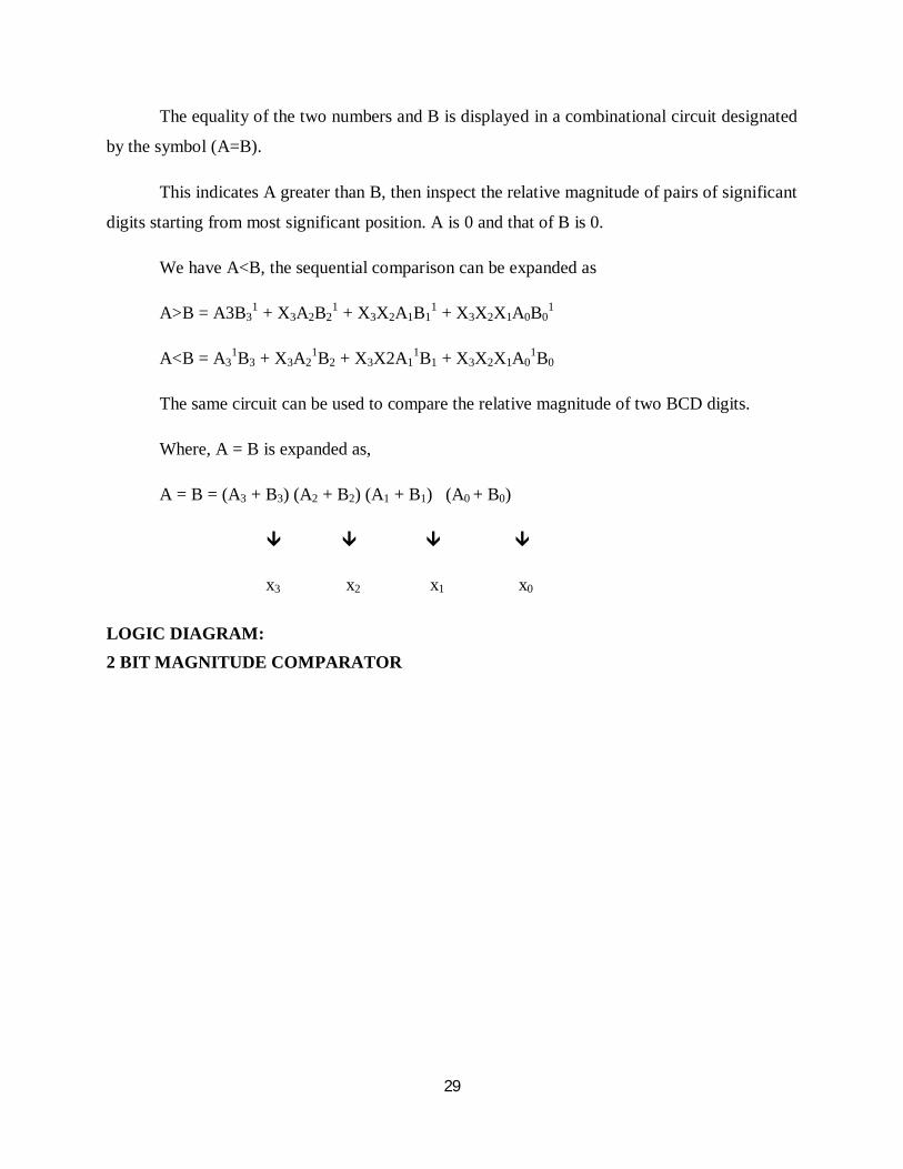
The equality of the two numbers and B is displayed in a combinational circuit designated
by the symbol (A=B).
This indicates A greater than B, then inspect the relative magnitude of pairs of significant
digits starting from most significant position. A is 0 and that of B is 0.
We have A<B, the sequential comparison can be expanded as
A>B = A3B31 + X3A2B2
1 + X3X2A1B11 + X3X2X1A0B0
1
A<B = A31B3 + X3A2
1B2 + X3X2A11B1 + X3X2X1A0
1B0
The same circuit can be used to compare the relative magnitude of two BCD digits.
Where, A = B is expanded as,
A = B = (A3 + B3) (A2 + B2) (A1 + B1) (A0 + B0)
x3 x2 x1 x0
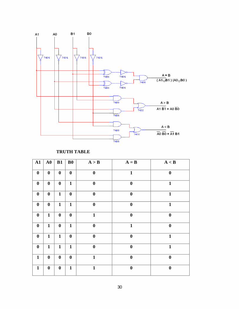
LOGIC DIAGRAM: 2 BIT MAGNITUDE COMPARATOR
30
TRUTH TABLE
A1 A0 B1 B0 A > B A = B A < B
0 0 0 0 0 1 0
0 0 0 1 0 0 1
0 0 1 0 0 0 1
0 0 1 1 0 0 1
0 1 0 0 1 0 0
0 1 0 1 0 1 0
0 1 1 0 0 0 1
0 1 1 1 0 0 1
1 0 0 0 1 0 0
1 0 0 1 1 0 0
31
1 0 1 0 0 1 0
1 0 1 1 0 0 1
1 1 0 0 1 0 0
1 1 0 1 1 0 0
1 1 1 0 1 0 0
1 1 1 1 0 1 0
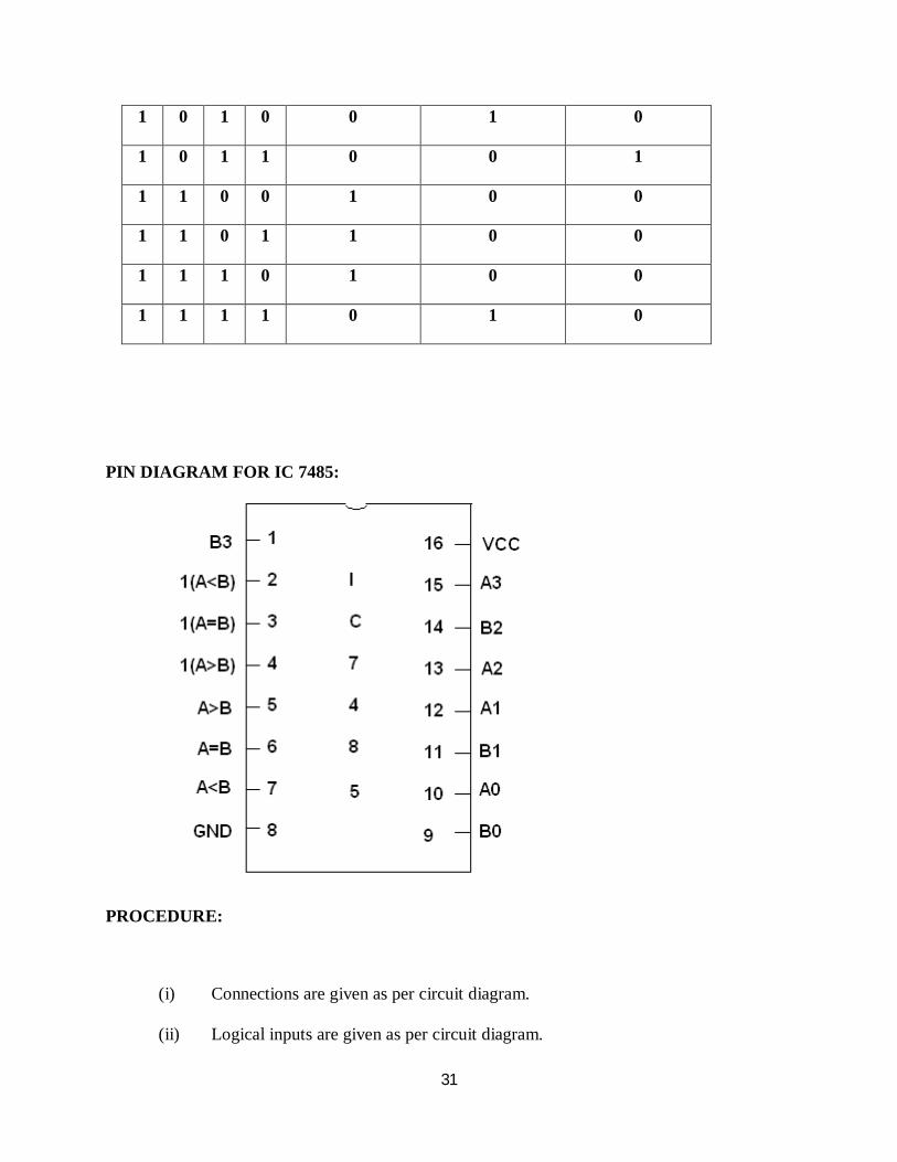
PIN DIAGRAM FOR IC 7485:
PROCEDURE:
(i) Connections are given as per circuit diagram.
(ii) Logical inputs are given as per circuit diagram.

32
(iii) Observe the output and verify the truth table.
RESULT:
33
Ex No:6 DATE :
16 BIT ODD/EVEN PARITY CHECKER /GENERATOR
AIM:
To design and implement 16 bit odd/even parity checker generator using IC 74180.
APPARATUS REQUIRED:
Sl.No. COMPONENT SPECIFICATION QTY.
1. NOT GATE IC 7404 1
IC 74180 2
2. IC TRAINER KIT - 1
3. PATCH CORDS - 30
THEORY:
A parity bit is used for detecting errors during transmission of binary information. A
parity bit is an extra bit included with a binary message to make the number is either even or
odd. The message including the parity bit is transmitted and then checked at the receiver ends for
errors. An error is detected if the checked parity bit doesn’t correspond to the one transmitted.
The circuit that generates the parity bit in the transmitter is called a ‘parity generator’ and the
circuit that checks the parity in the receiver is called a ‘parity checker’.
In even parity, the added parity bit will make the total number is even amount. In odd
parity, the added parity bit will make the total number is odd amount. The parity checker circuit
checks for possible errors in the transmission. If the information is passed in even parity, then the
bits required must have an even number of 1’s. An error occur during transmission, if the
received bits have an odd number of 1’s indicating that one bit has changed in value during
transmission.
34
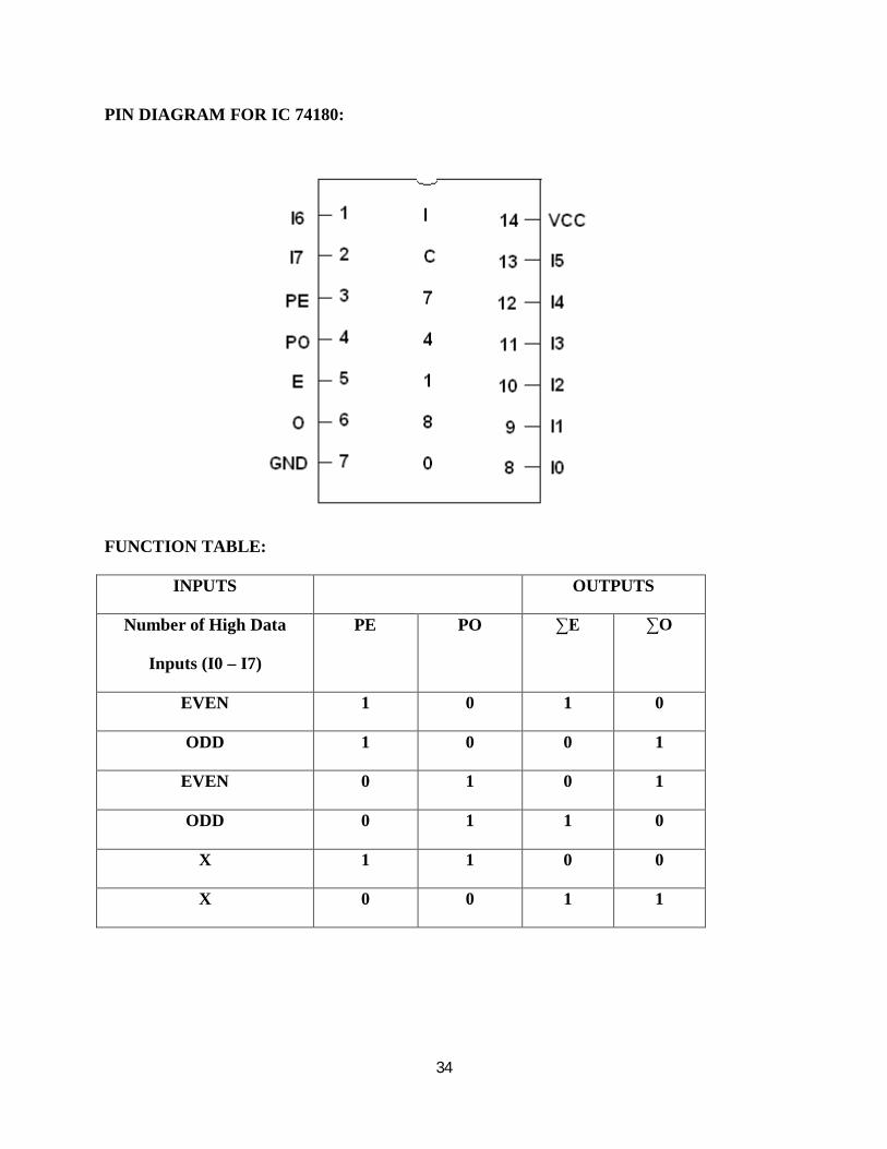
PIN DIAGRAM FOR IC 74180:
FUNCTION TABLE:
INPUTS OUTPUTS
Number of High Data
Inputs (I0 – I7)
PE PO ∑E ∑O
EVEN 1 0 1 0
ODD 1 0 0 1
EVEN 0 1 0 1
ODD 0 1 1 0
X 1 1 0 0
X 0 0 1 1
35
LOGIC DIAGRAM:
16 BIT ODD/EVEN PARITY CHECKER
TRUTH TABLE:
I7 I6 I5 I4 I3 I2 I1 I0 I7’I6’I5’I4’I3’I2’11’ I0’ Active ∑E ∑O
0 0 0 0 0 0 0 1 0 0 0 0 0 0 0 0 1 1 0
0 0 0 0 0 1 1 0 0 0 0 0 0 1 1 0 0 1 0
0 0 0 0 0 1 1 0 0 0 0 0 0 1 1 0 1 0 1
LOGIC DIAGRAM: 16 BIT ODD/EVEN PARITY GENERATOR
36
TRUTH TABLE:
I7 I6 I5 I4 I3 I2 I1 I0 I7 I6 I5 I4 I3 I2 I1 I0 Active ∑E ∑O
1 1 0 0 0 0 0 0 1 1 0 0 0 0 0 0 1 1 0
1 1 0 0 0 0 0 0 1 1 0 0 0 0 0 0 0 0 1
1 1 0 0 0 0 0 0 0 1 0 0 0 0 0 0 0 1 0
PROCEDURE:
(i) Connections are given as per circuit diagram.
(ii) Logical inputs are given as per circuit diagram.
(iii) Observe the output and verify the truth table.
RESULT:
37
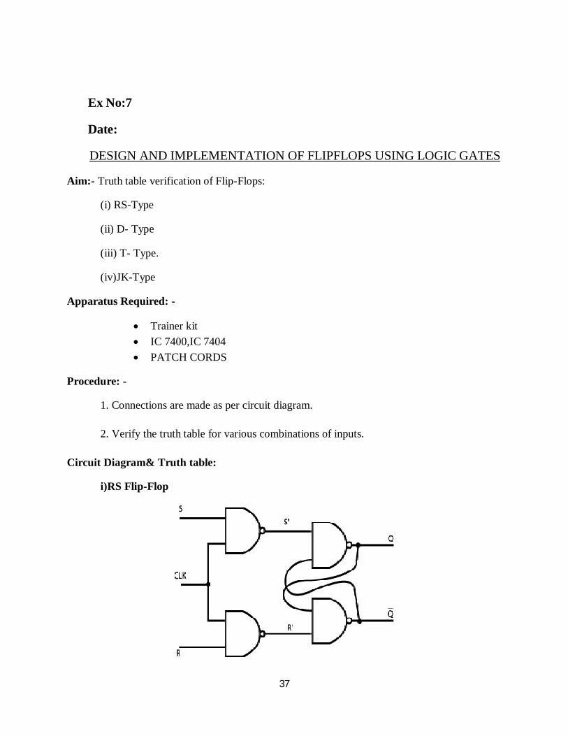
Ex No:7
Date:
DESIGN AND IMPLEMENTATION OF FLIPFLOPS USING LOGIC GATES
Aim:- Truth table verification of Flip-Flops:
(i) RS-Type
(ii) D- Type
(iii) T- Type.
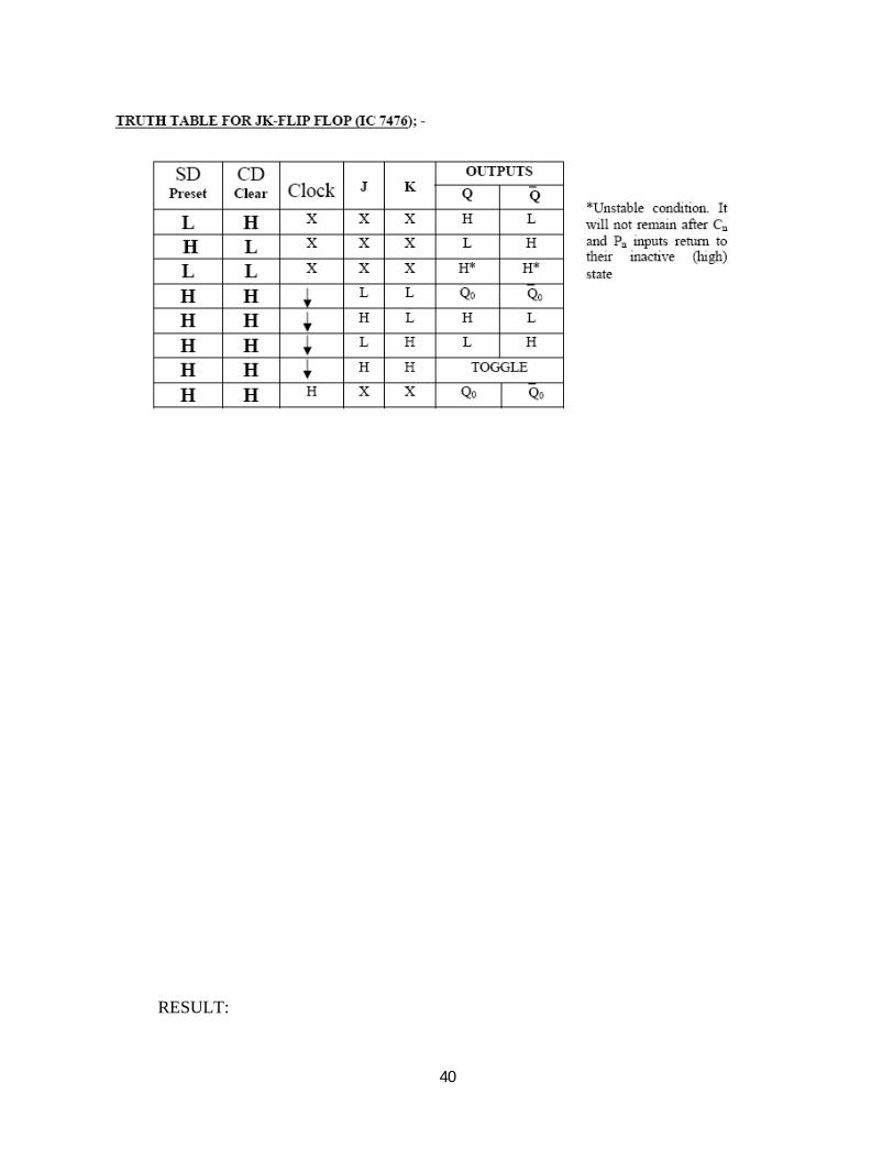
(iv)JK-Type
Apparatus Required: -
Trainer kit IC 7400,IC 7404 PATCH CORDS
Procedure: -
1. Connections are made as per circuit diagram.
2. Verify the truth table for various combinations of inputs.
Circuit Diagram& Truth table:
i)RS Flip-Flop
38
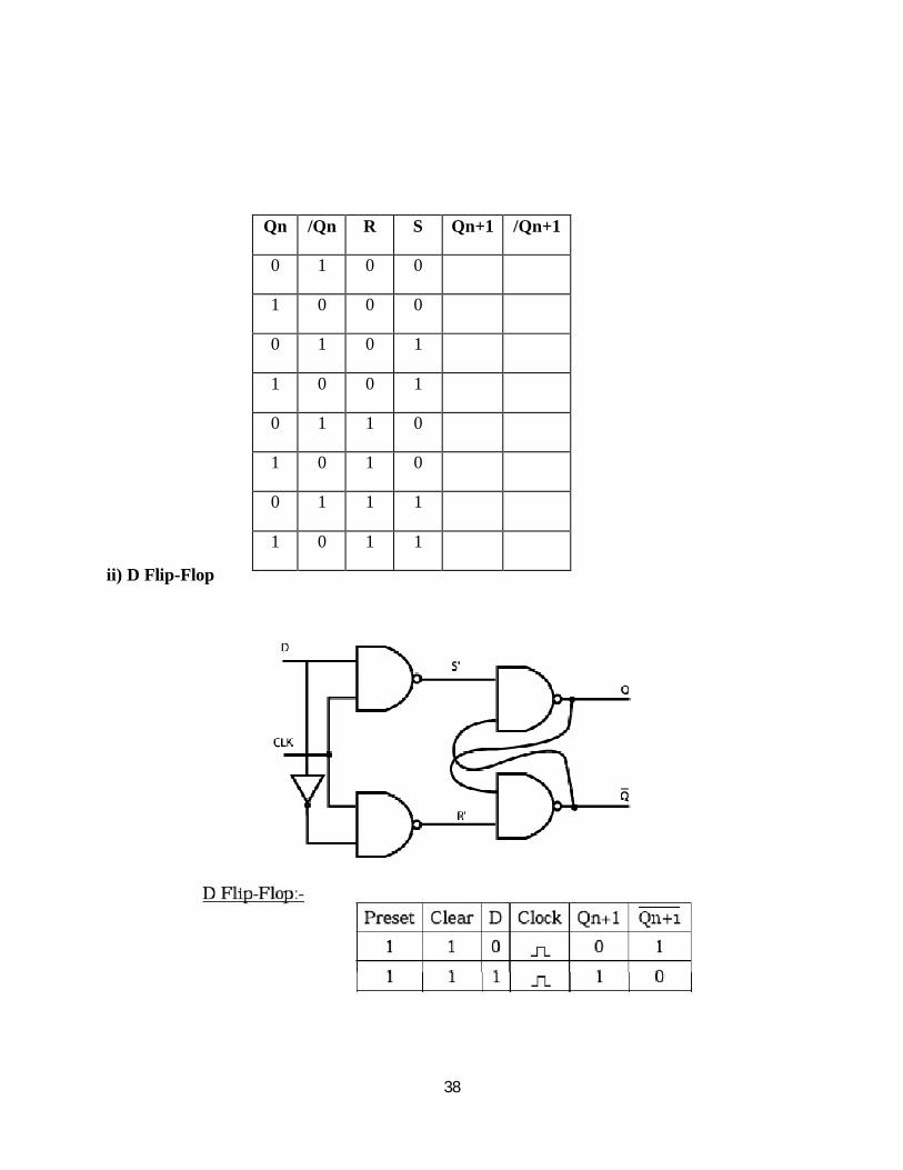
ii) D Flip-Flop
Qn /Qn R S Qn+1 /Qn+1
0 1 0 0
1 0 0 0
0 1 0 1
1 0 0 1
0 1 1 0
1 0 1 0
0 1 1 1
1 0 1 1
39
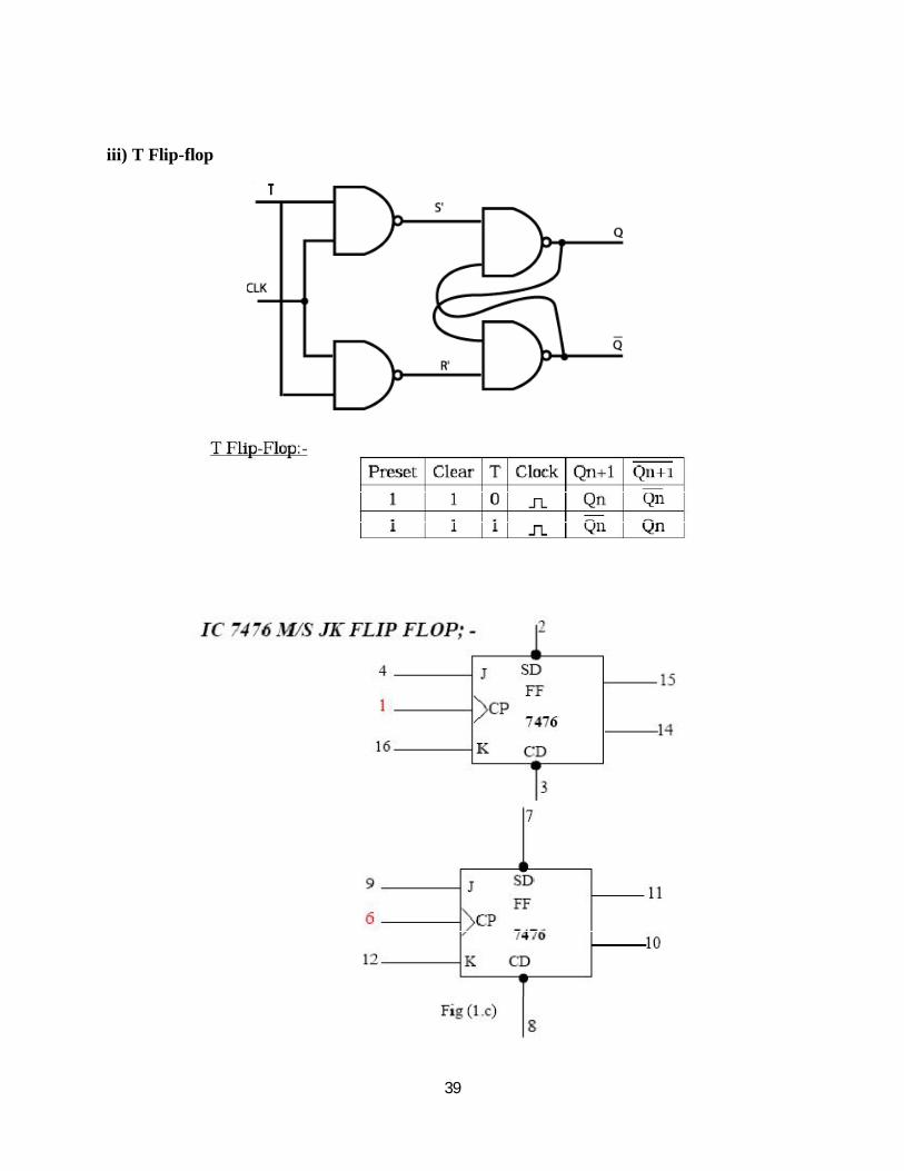
iii) T Flip-flop
40
RESULT:
41
Ex No. :8 DATE :
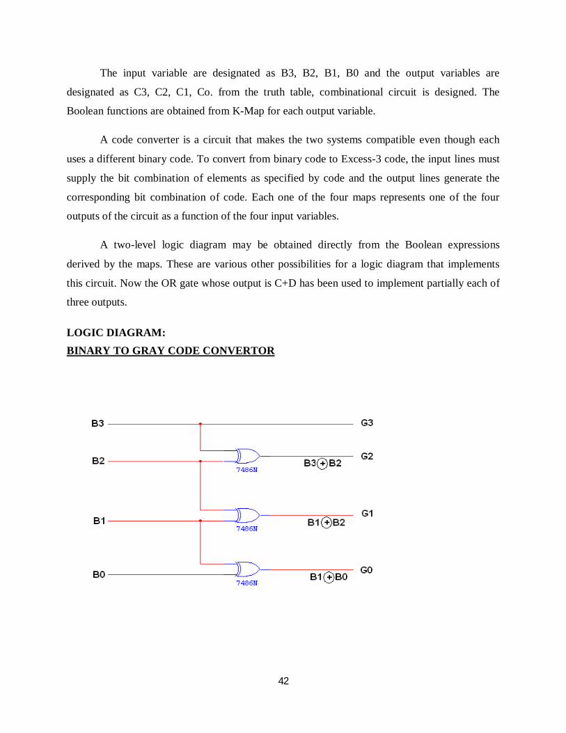
DESIGN AND IMPLEMENTATION OF CODE CONVERTOR AIM:
To design and implement 4-bit
(i) Binary to gray code converter (ii) Gray to binary code converter (iii) BCD to excess-3 code converter (iv) Excess-3 to BCD code converter
APPARATUS REQUIRED:
Sl.No. COMPONENT SPECIFICATION QTY.
1. X-OR GATE IC 7486 1
2. AND GATE IC 7408 1
3. OR GATE IC 7432 1
4. NOT GATE IC 7404 1
5. IC TRAINER KIT - 1
6. PATCH CORDS - 35
THEORY:
The availability of large variety of codes for the same discrete elements of information
results in the use of different codes by different systems. A conversion circuit must be inserted
between the two systems if each uses different codes for same information. Thus, code converter
is a circuit that makes the two systems compatible even though each uses different binary code.
The bit combination assigned to binary code to gray code. Since each code uses four bits
to represent a decimal digit. There are four inputs and four outputs. Gray code is a non-weighted
code.
42
The input variable are designated as B3, B2, B1, B0 and the output variables are
designated as C3, C2, C1, Co. from the truth table, combinational circuit is designed. The
Boolean functions are obtained from K-Map for each output variable.
A code converter is a circuit that makes the two systems compatible even though each
uses a different binary code. To convert from binary code to Excess-3 code, the input lines must
supply the bit combination of elements as specified by code and the output lines generate the
corresponding bit combination of code. Each one of the four maps represents one of the four
outputs of the circuit as a function of the four input variables.
A two-level logic diagram may be obtained directly from the Boolean expressions
derived by the maps. These are various other possibilities for a logic diagram that implements
this circuit. Now the OR gate whose output is C+D has been used to implement partially each of
three outputs.
LOGIC DIAGRAM: BINARY TO GRAY CODE CONVERTOR
43
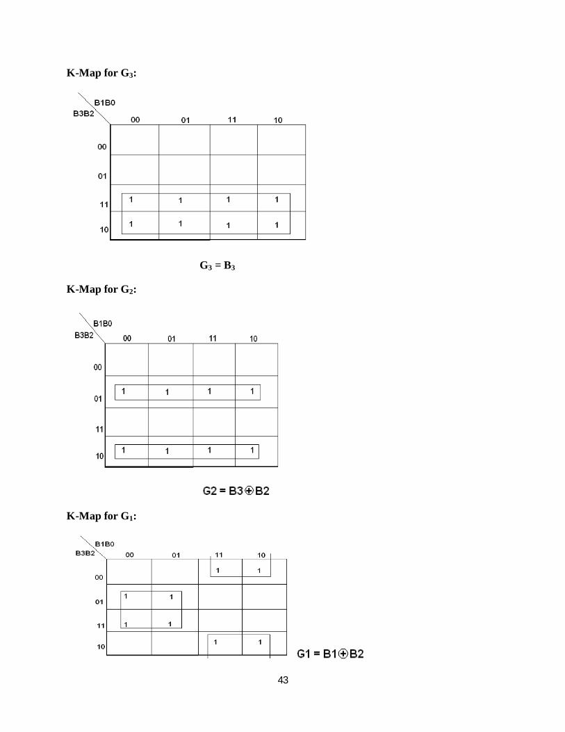
K-Map for G3:
G3 = B3
K-Map for G2:
K-Map for G1:
44
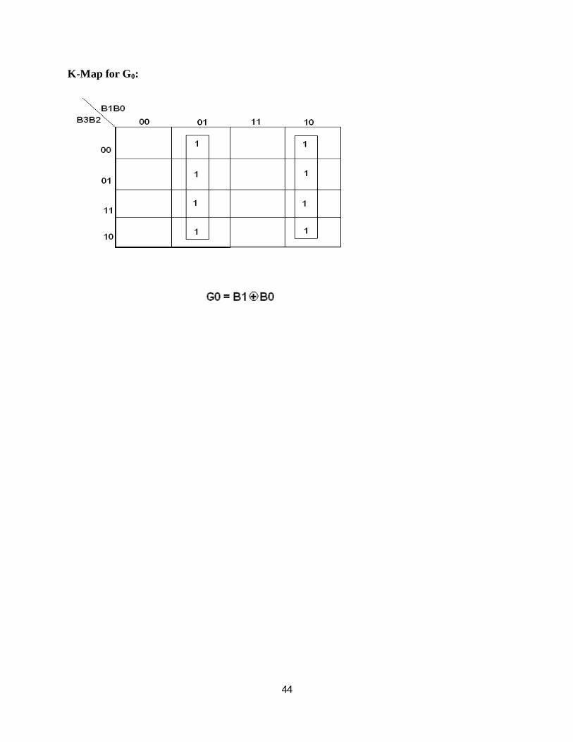
K-Map for G0:
45
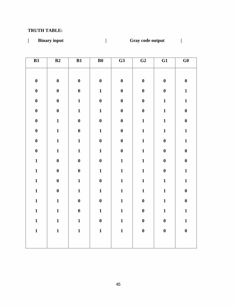
TRUTH TABLE:
| Binary input | Gray code output |
B3 B2 B1 B0 G3 G2 G1 G0
0
0
0
0
0
0
0
0
1
1
1
1
1
1
1
1
0
0
0
0
1
1
1
1
0
0
0
0
1
1
1
1
0
0
1
1
0
0
1
1
0
0
1
1
0
0
1
1
0
1
0
1
0
1
0
1
0
1
0
1
0
1
0
1
0
0
0
0
0
0
0
0
1
1
1
1
1
1
1
1
0
0
0
0
1
1
1
1
1
1
1
1
0
0
0
0
0
0
1
1
1
1
0
0
0
0
1
1
1
1
0
0
0
1
1
0
0
1
1
0
0
1
1
0
0
1
1
0
46
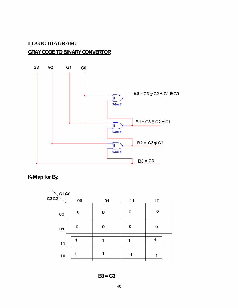
LOGIC DIAGRAM: GRAY CODE TO BINARY CONVERTOR
K-Map for B3:
B3 = G3
47
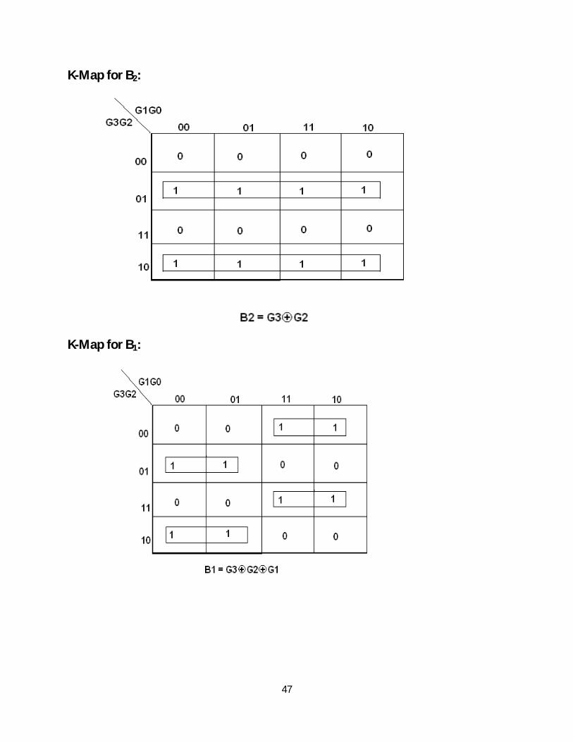
K-Map for B2:
K-Map for B1:
48
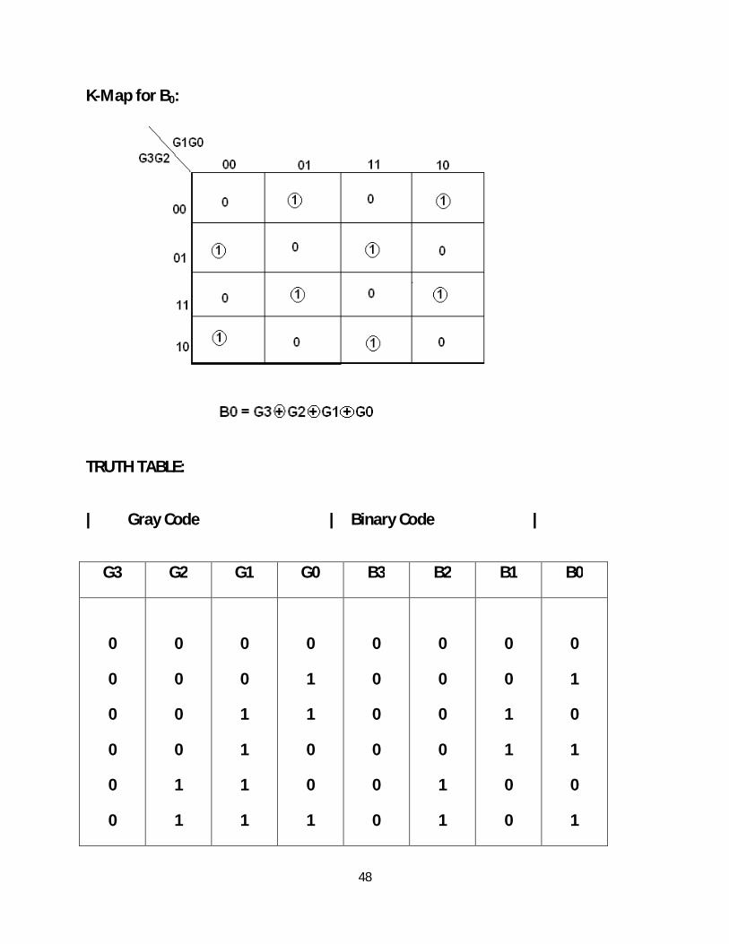
K-Map for B0:
TRUTH TABLE:
| Gray Code | Binary Code |
G3 G2 G1 G0 B3 B2 B1 B0
0
0
0
0
0
0
0
0
0
0
1
1
0
0
1
1
1
1
0
1
1
0
0
1
0
0
0
0
0
0
0
0
0
0
1
1
0
0
1
1
0
0
0
1
0
1
0
1
49
0
0
1
1
1
1
1
1
1
1
1
1
1
1
1
1
0
0
0
0
0
0
0
0
1
1
1
1
0
0
1
0
0
1
1
0
0
1
1
0
0
0
1
1
1
1
1
1
1
1
1
1
0
0
0
0
1
1
1
1
1
1
0
0
1
1
0
0
1
1
0
1
0
1
0
1
0
1
0
1
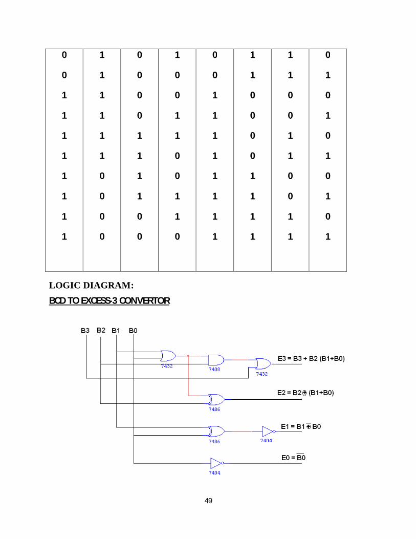
LOGIC DIAGRAM: BCD TO EXCESS-3 CONVERTOR
50
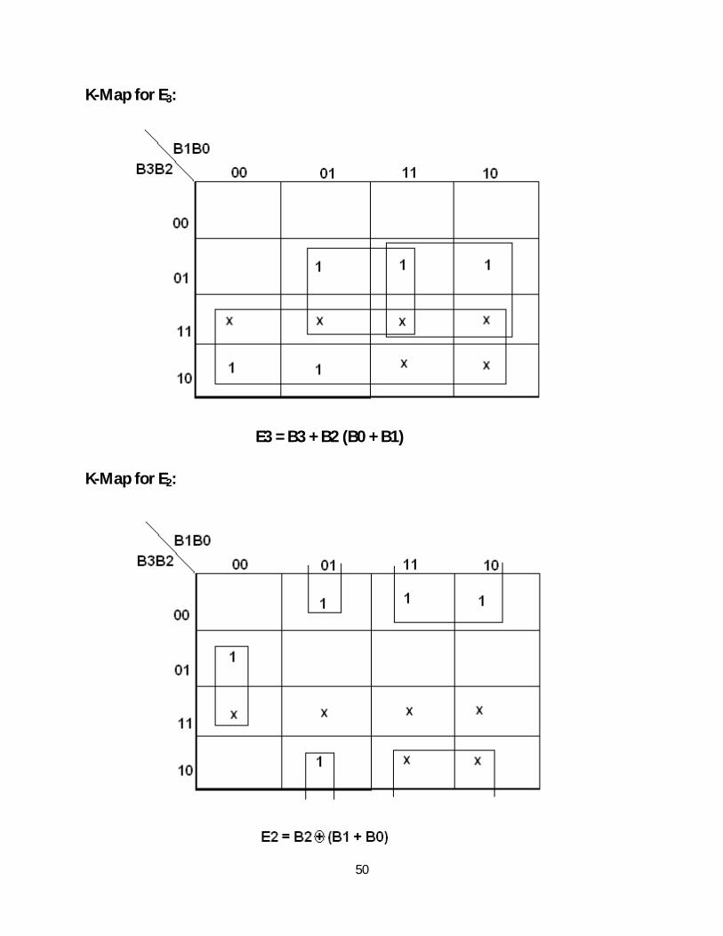
K-Map for E3:
E3 = B3 + B2 (B0 + B1)
K-Map for E2:
51
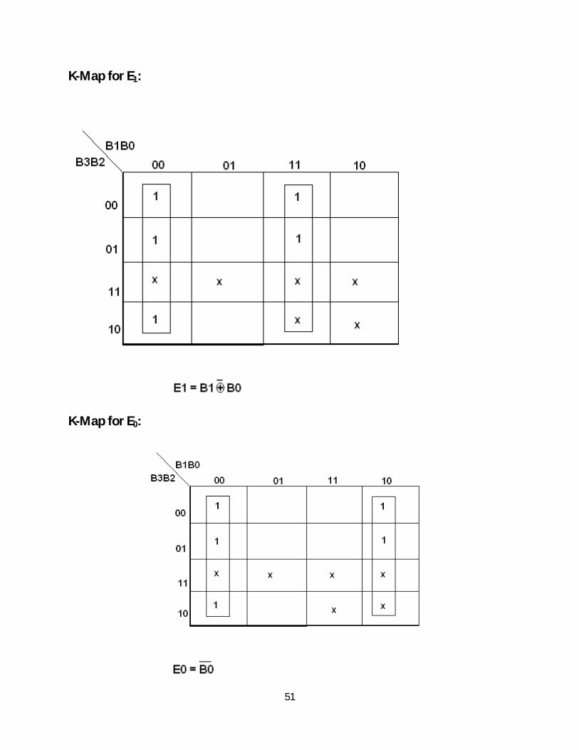
K-Map for E1:
K-Map for E0:
52
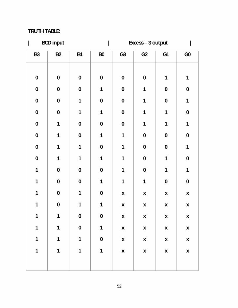
TRUTH TABLE:
| BCD input | Excess – 3 output |
B3 B2 B1 B0 G3 G2 G1 G0
0
0
0
0
0
0
0
0
1
1
1
1
1
1
1
1
0
0
0
0
1
1
1
1
0
0
0
0
1
1
1
1
0
0
1
1
0
0
1
1
0
0
1
1
0
0
1
1
0
1
0
1
0
1
0
1
0
1
0
1
0
1
0
1
0
0
0
0
0
1
1
1
1
1
x
x
x
x
x
x
0
1
1
1
1
0
0
0
0
1
x
x
x
x
x
x
1
0
0
1
1
0
0
1
1
0
x
x
x
x
x
x
1
0
1
0
1
0
1
0
1
0
x
x
x
x
x
x
53
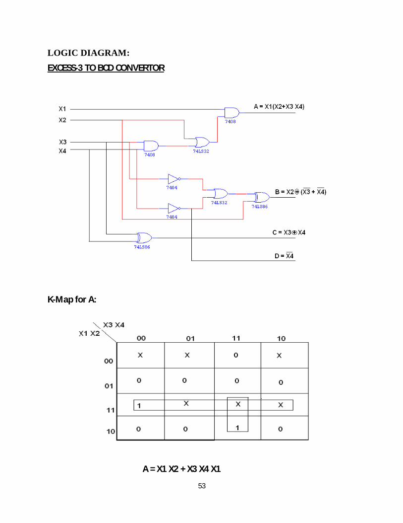
LOGIC DIAGRAM: EXCESS-3 TO BCD CONVERTOR
K-Map for A:
A = X1 X2 + X3 X4 X1
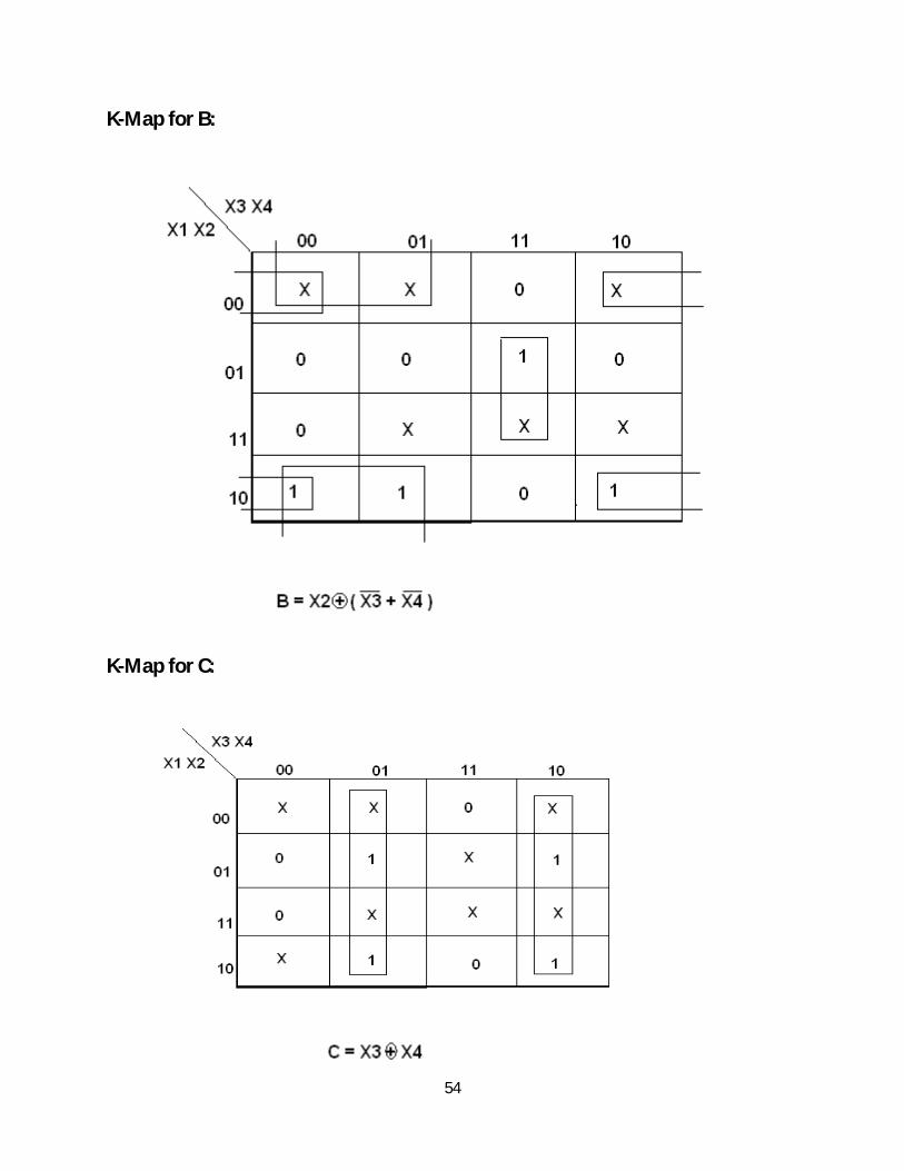
54
K-Map for B:
K-Map for C:
55
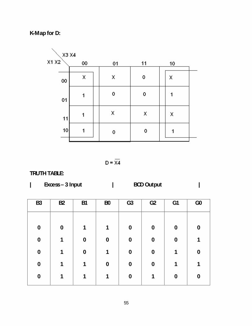
K-Map for D:
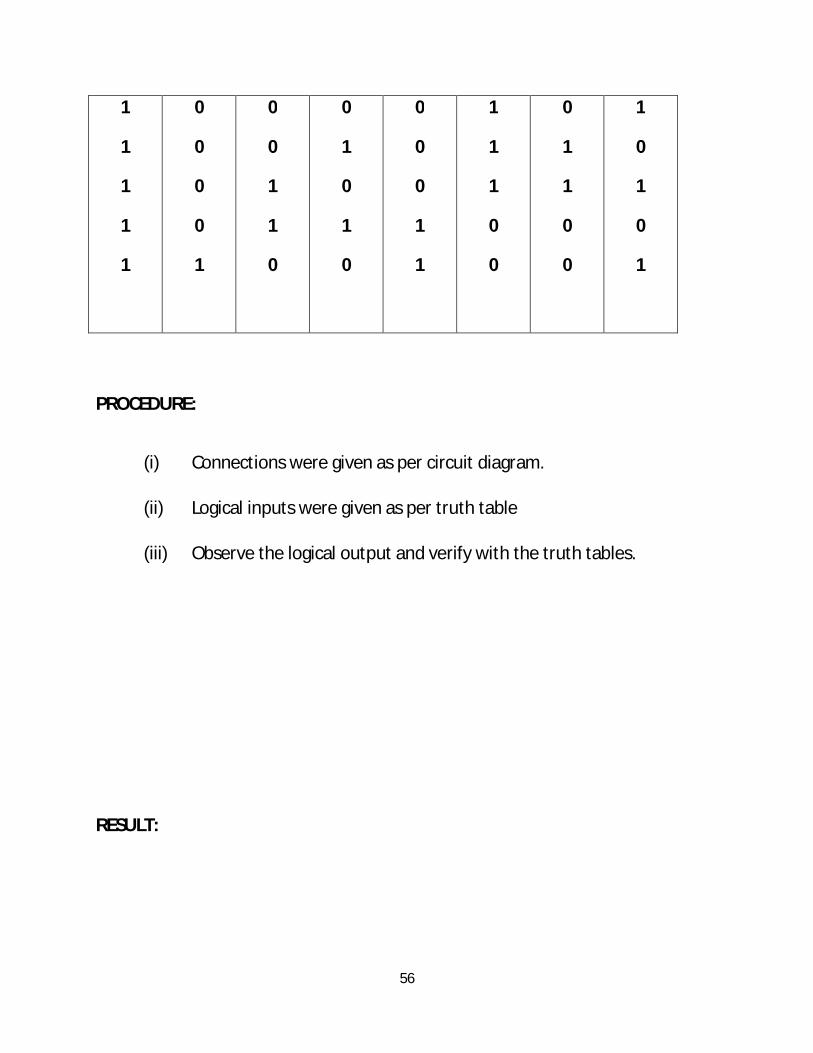
TRUTH TABLE:
| Excess – 3 Input | BCD Output |
B3 B2 B1 B0 G3 G2 G1 G0
0
0
0
0
0
0
1
1
1
1
1
0
0
1
1
1
0
1
0
1
0
0
0
0
0
0
0
0
0
1
0
0
1
1
0
0
1
0
1
0
56
1
1
1
1
1
0
0
0
0
1
0
0
1
1
0
0
1
0
1
0
0
0
0
1
1
1
1
1
0
0
0
1
1
0
0
1
0
1
0
1
PROCEDURE:
(i) Connections were given as per circuit diagram.
(ii) Logical inputs were given as per truth table
(iii) Observe the logical output and verify with the truth tables.
RESULT:

57
Ex No:9 Date :
CONSTRUCTION AND VERIFICATION OF 4 BIT RIPPLE COUNTER AND MOD 10/MOD 12 RIPPLE COUNTER
AIM:
To design and verify 4 bit ripple counter mod 10/ mod 12 ripple counter.
APPARATUS REQUIRED:
Sl.No. COMPONENT SPECIFICATION QTY.
1. JK FLIP FLOP IC 7476 2
2. NAND GATE IC 7400 1
3. IC TRAINER KIT - 1
4. PATCH CORDS - 30
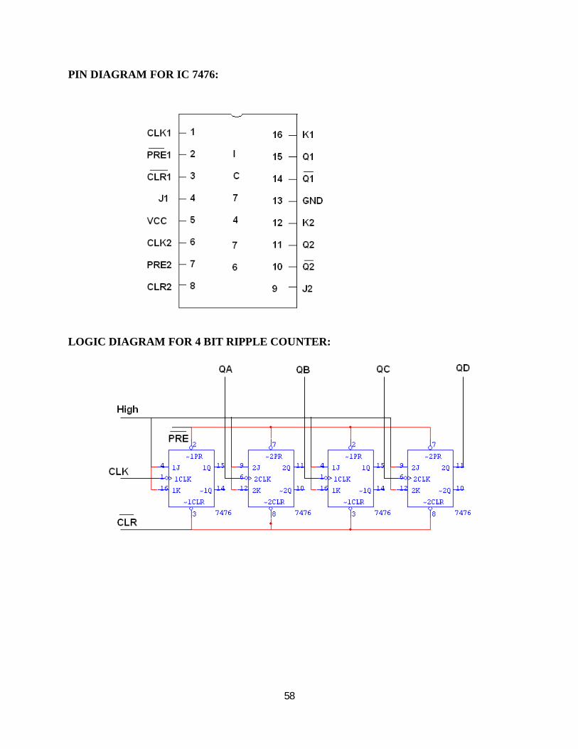
THEORY:
A counter is a register capable of counting number of clock pulse arriving at its clock
input. Counter represents the number of clock pulses arrived. A specified sequence of states
appears as counter output. This is the main difference between a register and a counter. There are
two types of counter, synchronous and asynchronous. In synchronous common clock is given to
all flip flop and in asynchronous first flip flop is clocked by external pulse and then each
successive flip flop is clocked by Q or Q output of previous stage. A soon the clock of second
stage is triggered by output of first stage. Because of inherent propagation delay time all flip
flops are not activated at same time which results in asynchronous operation.
58
PIN DIAGRAM FOR IC 7476:
LOGIC DIAGRAM FOR 4 BIT RIPPLE COUNTER:
59
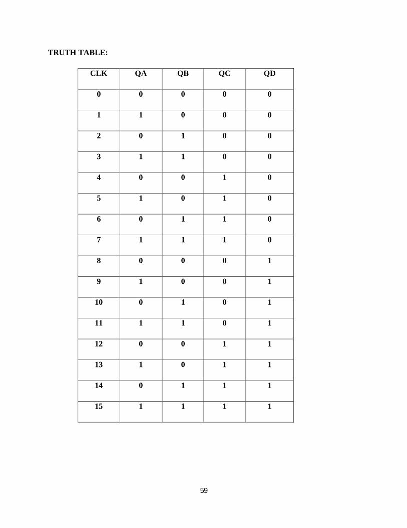
TRUTH TABLE:
CLK QA QB QC QD
0 0 0 0 0
1 1 0 0 0
2 0 1 0 0
3 1 1 0 0
4 0 0 1 0
5 1 0 1 0
6 0 1 1 0
7 1 1 1 0
8 0 0 0 1
9 1 0 0 1
10 0 1 0 1
11 1 1 0 1
12 0 0 1 1
13 1 0 1 1
14 0 1 1 1
15 1 1 1 1
60
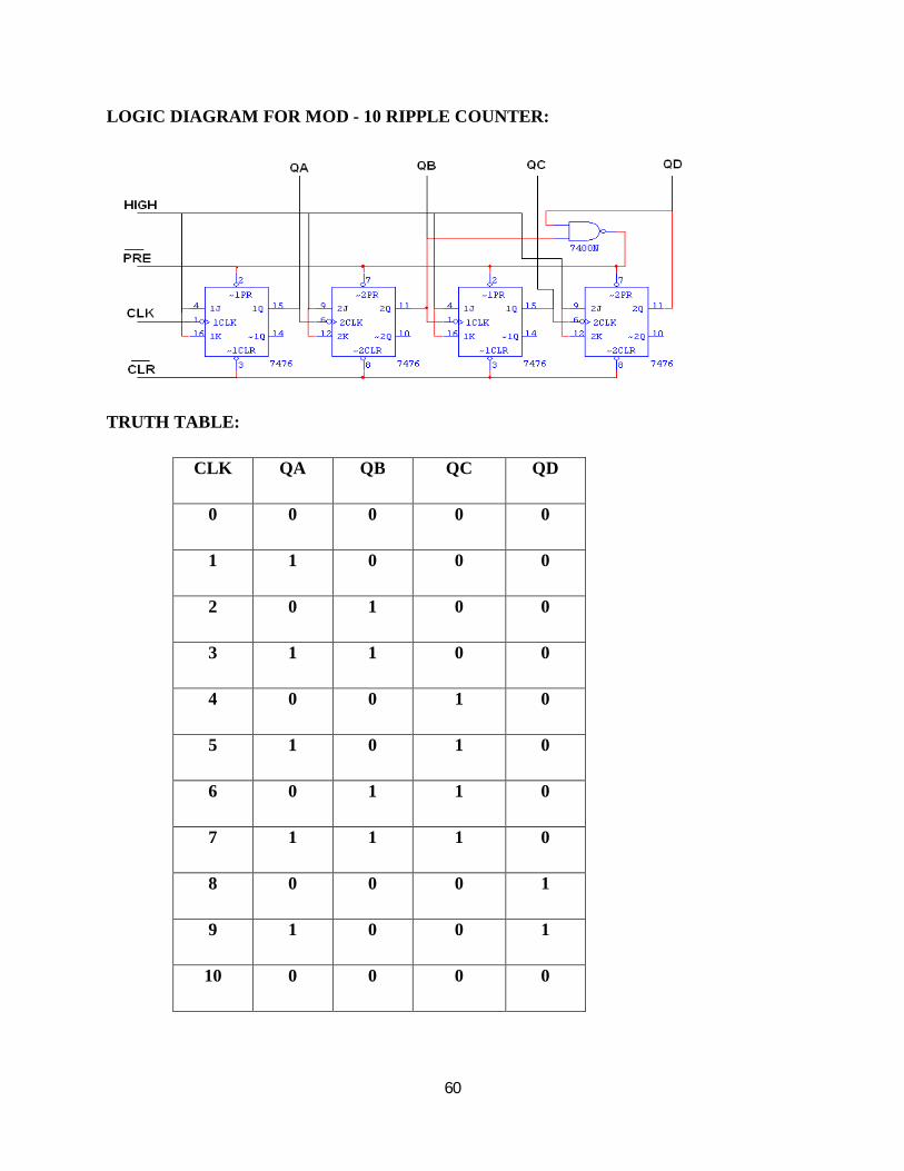
LOGIC DIAGRAM FOR MOD - 10 RIPPLE COUNTER:
TRUTH TABLE:
CLK QA QB QC QD
0 0 0 0 0
1 1 0 0 0
2 0 1 0 0
3 1 1 0 0
4 0 0 1 0
5 1 0 1 0
6 0 1 1 0
7 1 1 1 0
8 0 0 0 1
9 1 0 0 1
10 0 0 0 0
61
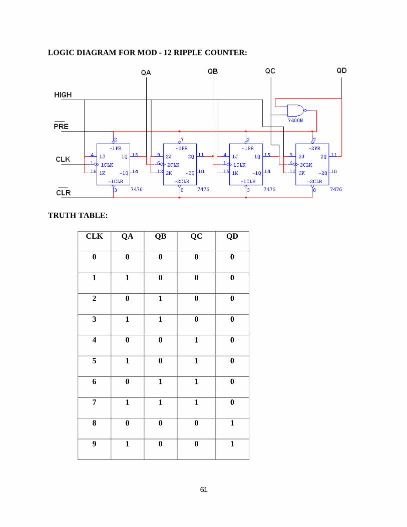
LOGIC DIAGRAM FOR MOD - 12 RIPPLE COUNTER:
TRUTH TABLE:
CLK QA QB QC QD
0 0 0 0 0
1 1 0 0 0
2 0 1 0 0
3 1 1 0 0
4 0 0 1 0
5 1 0 1 0
6 0 1 1 0
7 1 1 1 0
8 0 0 0 1
9 1 0 0 1

62
10 0 1 0 1
11 1 1 0 1
12 0 0 0 0
PROCEDURE:
(i) Connections are given as per circuit diagram.
(ii) Logical inputs are given as per circuit diagram.
(iii) Observe the output and verify the truth table.
RESULT:

63
Ex No :9(b) DATE :
DESIGN AND IMPLEMENTATION OF 3 BIT SYNCHRONOUS UP/DOWN COUNTER
AIM:
To design and implement 3 bit synchronous up/down counter.
APPARATUS REQUIRED:
Sl.No. COMPONENT SPECIFICATION QTY.
1. JK FLIP FLOP IC 7476 2
2. 3 I/P AND GATE IC 7411 1
3. OR GATE IC 7432 1
4. XOR GATE IC 7486 1
5. NOT GATE IC 7404 1
6. IC TRAINER KIT - 1
7. PATCH CORDS - 35
THEORY:
A counter is a register capable of counting number of clock pulse arriving at its clock
input. Counter represents the number of clock pulses arrived. An up/down counter is one that is
capable of progressing in increasing order or decreasing order through a certain sequence. An
up/down counter is also called bidirectional counter. Usually up/down operation of the counter is
controlled by up/down signal. When this signal is high counter goes through up sequence and
when up/down signal is low counter follows reverse sequence.
64
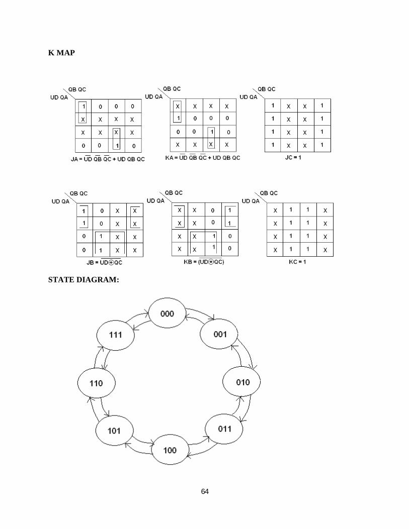
K MAP
STATE DIAGRAM:
65
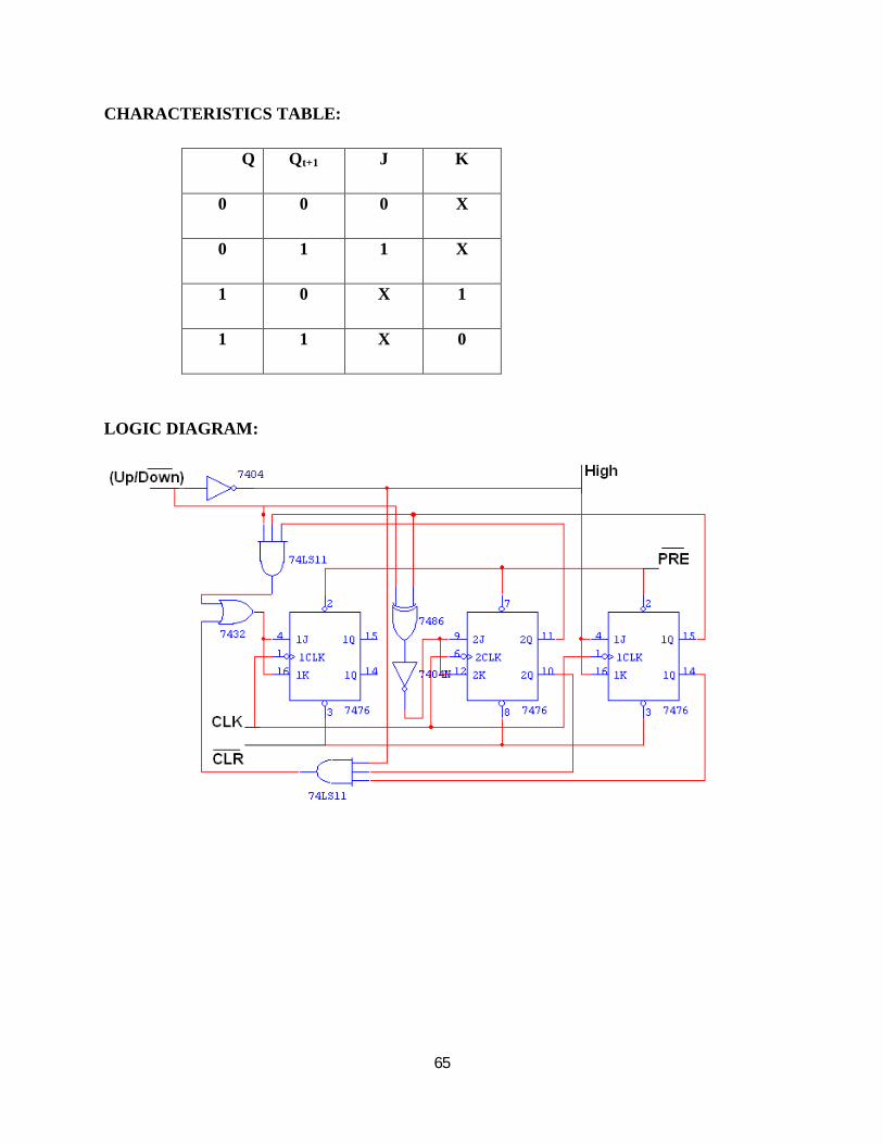
CHARACTERISTICS TABLE:
Q Qt+1 J K
0 0 0 X
0 1 1 X
1 0 X 1
1 1 X 0
LOGIC DIAGRAM:
66
TRUTH TABLE:
Input
Up/Down
Present State
QA QB QC
Next State
QA+1 Q B+1 QC+1
A
JA KA
B
JB KB
C
JC KC
0 0 0 0 1 1 1 1 X 1 X 1 X
0 1 1 1 1 1 0 X 0 X 0 X 1
0 1 1 0 1 0 1 X 0 X 1 1 X
0 1 0 1 1 0 0 X 0 0 X X 1
0 1 0 0 0 1 1 X 1 1 X 1 X
0 0 1 1 0 1 0 0 X X 0 X 1
0 0 1 0 0 0 1 0 X X 1 1 X
0 0 0 1 0 0 0 0 X 0 X X 1
1 0 0 0 0 0 1 0 X 0 X 1 X
1 0 0 1 0 1 0 0 X 1 X X 1
1 0 1 0 0 1 1 0 X X 0 1 X
1 0 1 1 1 0 0 1 X X 1 X 1
1 1 0 0 1 0 1 X 0 0 X 1 X
1 1 0 1 1 1 0 X 0 1 X X 1
1 1 1 0 1 1 1 X 0 X 0 1 X
1 1 1 1 0 0 0 X 1 X 1 X 1

67
PROCEDURE:
(i) Connections are given as per circuit diagram.
(ii) Logical inputs are given as per circuit diagram.
(iii) Observe the output and verify the truth table.
RESULT:

68
Ex No:10 Date :
DESIGN AND IMPLEMENTATION OF SHIFT REGISTER
AIM:
To design and implement
(i) Serial in serial out (ii) Serial in parallel out (iii) Parallel in serial out (iv) Parallel in parallel out
APPARATUS REQUIRED:
Sl.No.
COMPONENT SPECIFICATION QTY.
1. D FLIP FLOP IC 7474 2
2. OR GATE IC 7432 1
3. IC TRAINER KIT - 1
4. PATCH CORDS - 35
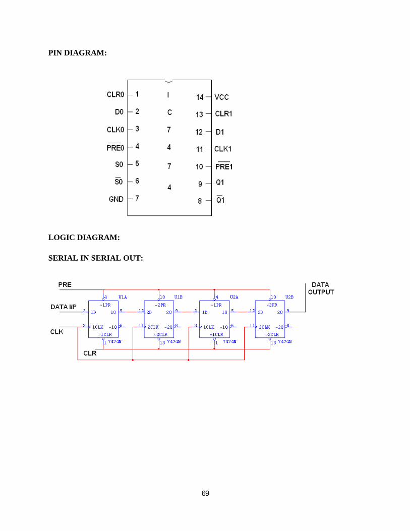
THEORY:
A register is capable of shifting its binary information in one or both directions is known
as shift register. The logical configuration of shift register consist of a D-Flip flop cascaded with
output of one flip flop connected to input of next flip flop. All flip flops receive common clock
pulses which causes the shift in the output of the flip flop. The simplest possible shift register is
one that uses only flip flop. The output of a given flip flop is connected to the input of next flip
flop of the register. Each clock pulse shifts the content of register one bit position to right.
69
PIN DIAGRAM:
LOGIC DIAGRAM:
SERIAL IN SERIAL OUT:
70
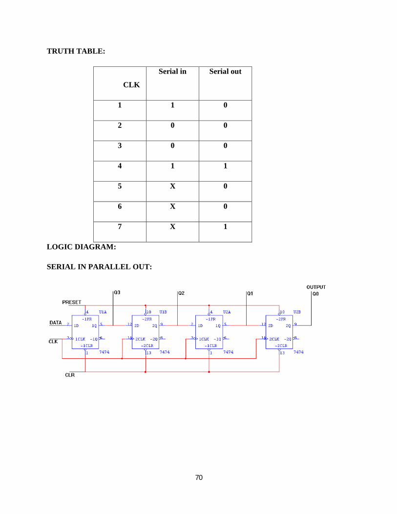
TRUTH TABLE:
CLK
Serial in Serial out
1 1 0
2 0 0
3 0 0
4 1 1
5 X 0
6 X 0
7 X 1
LOGIC DIAGRAM:
SERIAL IN PARALLEL OUT:
71
TRUTH TABLE:
CLK
DATA
OUTPUT
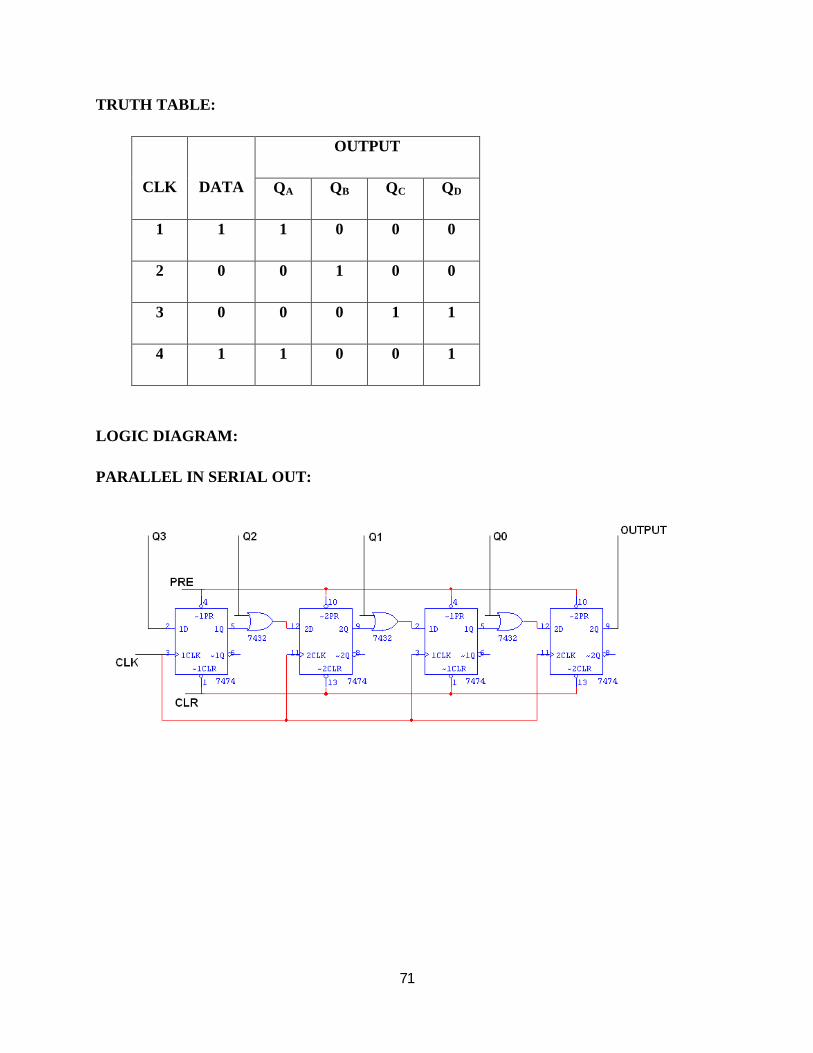
QA QB QC QD
1 1 1 0 0 0
2 0 0 1 0 0
3 0 0 0 1 1
4 1 1 0 0 1
LOGIC DIAGRAM:
PARALLEL IN SERIAL OUT:
72
TRUTH TABLE:
CLK Q3 Q2 Q1 Q0 O/P
0 1 0 0 1 1
1 0 0 0 0 0
2 0 0 0 0 0
3 0 0 0 0 1
LOGIC DIAGRAM:
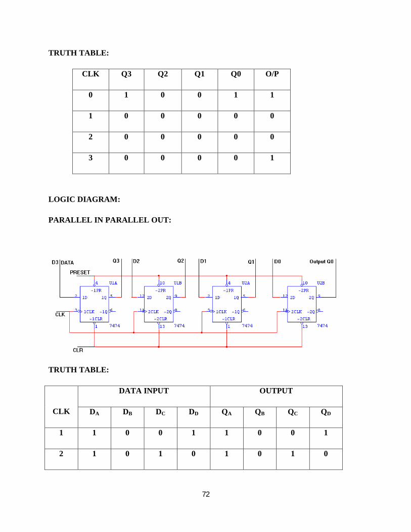
PARALLEL IN PARALLEL OUT:
TRUTH TABLE:
CLK
DATA INPUT OUTPUT
DA DB DC DD QA QB QC QD
1 1 0 0 1 1 0 0 1
2 1 0 1 0 1 0 1 0

73
PROCEDURE:
(i) Connections are given as per circuit diagram.
(ii) Logical inputs are given as per circuit diagram.
(iii) Observe the output and verify the truth table.
RESULT: