department of electrical engineering … of electrical engineering stanford university * stanford....
TRANSCRIPT

i- ,
I -'
~ ~ ~ ~ ~ ~ ~~~
/A?-?- P@4$p" Q 9-*
DEPARTMENT OF ELECTRICAL ENGINEERING STANFORD UNIVERSITY * STANFORD. CA 94305 FINAL REPORT
SUBMllTED TO
JET PROPULSION LABORATORY PASADENA, CA
CONTRACT TITLE
MEASUREMENT OF CARRIER TRANSPORT AND RECOMBINATION PARAMETER IN HEAVILY DOPED SILICON
Minority Carrier Transport in Heavily Doped n-Typed Silicon Jesus A. del Alamo, Volume I (submitted earlier)
Minority Carrier Transport in Heavily Doped Si:B Stanley E. Swirhun and Richard M. Swanson, Volume II
BY
STANFORD UNlVERSlN STANFORD, CA 94305
FOR PERIOD 2 APRIL 1985 THROUGH 30 JUNE 1986 CONTRACT NO. 957159
R. M. SWANSON PRlNC I PAL INVESTIGATOR STANFORD ELECTRONICS LABORATORIES
The JPL Flat-Plate Solar Array Project is sponsored by the U.S. Department of Energy and forms part of the Solar Photovoltaic Conversion Program to initiate a major effort toward the development of low-cost solar arrays. This work was performed for the Jet Propulsion Laboratory, California Institute of Technology, by agreement between NASA and DOE.
m 0 r? =t n( W O N a-
4 CY U-
t f- m Q O a 30
li
https://ntrs.nasa.gov/search.jsp?R=19870012870 2018-05-16T01:49:48+00:00Z

This work was performed for the Jet Propulsion Laboratory, California Institute of Technology, and was sponsored by the U. S. Department of Energy through an agreement with the National Aeronautics and Space Ad mi n is trat i o n .
This report was prepared as an account of this work sponsored by an agency of the United States Government. Neither the United States Government nor any agency thereof, nor any of their employees, makes any warranty, express or implied, or assumes any legal liability or responsibility for the accuracy, completeness, or usefulness of any information, apparatus, product, or process disclosed, or represents that its use would not infringe privately owned rights.
Reference herein to any specific commercial product, process, or service by trade name, trademark, manufacturer, or otherwise, does not necessarily constitute or imply its endorsement, recommendation, or favoring by the United States Government or any agency thereof. The views and opinions of authors expressed herein do not necessarily state or reflect those of the United States Government or any agency thereof.

Abstract
The minority carrier transport and recombination parameters in heavily doped bulk silicon have been measured. Both Si:P and Si:B with bulk dopings from lo" to lozo cm" have been studied.
It is shown that three parameters characterize transport in bulk heavily doped Si: the minority carrier lifetime r, the minority carrier mobility c, and the equilibrium minority carrier density no or po (in p type and n-type Si respectively). Knowledge of no and po is equivalent to knowledge of bandgap narrowing AEG(NA) and AEG(ND). How- ever, dc current-voltage measurements can never measure all three of these parameters, and some M or timetransient experiment is required to obtain the values of these parameters as a function of dopant density.
Using both dc electrical measurements on bipolar transistors with heavily doped base regions and transient optical measurements on heav- ily doped bulk and epitaxially grown samples, lifetime, mobility and bandgap narrowing have been measured as a function of both p and n type dopant densities. Some interesting results:
1. Minority carrier electron and hole mobilities in heavily doped p and n-type Si are approximately a factor of two higher than the mobilities of these carriers as majority carriers. These are the first measurements of minority carrier mobility in the highly doped range.
2. Band-gap narrowing in n-type Si is negligible up to the lOl8 d o p ing level, and reaches almost 100 meV at lo2' cm". In ptype Si, band-gap narrowing exists as low as 1017 and reaches 120 meV at
3. Minority carrier lifetimes in processed heavily doped Si are best modeled by lifetime dependencies on doping that differ from the commonly used "band to band Auger" dependence.
Best fits of minority carrier mobility, band-gap narrowing and life- time as a function of doping density (in the heavily doped range) have been constructed to d o w accurate modeling of minority carrier trans- port in heavily doped Si.
cm+.

Minority Carrier Transport in Heavily Doped Si:B
VOl. I1
Stanley E. Swirhun and Richard M. Swanson Stanford University
Prepared for the Jet Propulsion Laboratory
October 13, 1986

Contents
1 Introduction 2
1.1 Scope . . . . . . . . . . . . . . . . . . . . . . . . . . . . . . . 2
1.2 Comparison of Si:B to Si:P . . . . . . . . . . . . . . . . . . . 4
2 Characterization of Bulk p+ Si:B 6
2.1 Minority Carrier Lifetime . . . . . . . . . . . . . . . . . . . . 6
2.2 Diffusion Length and Diffusion Coefficient . . . . . . . . . . . 16
3 Characterization of Epitaxial Si:B 23
3.1 Epitaxial Growth . . . . . . . . . . . . . . . . . . . . . . . . . 23
3.2 Bandgap Narrowing in p+ Si:B Epitaxial Layers. . . . . . . . 30
4 Conclusions 35
1

. .
Chapter 1
Introduction
1.1 Scope
This report summarizes work done under JPL contract JPL 957159 concern- ing the characterization of minority carrier transport and recombination in heavily doped Si. This part of the report (Vol. 11) discusses the results of a detailed investigation of the minority carrier transport parameters in heavily doped Si:B. A previous report “Minority Carrier Transport in Heavily Doped n-type Silicon”, Vol. I of this two part study, details the results on heavily doped Si:P.
The experimental work reported here is in two parts: optical measure- ments and electrical measurements. The portion concerning electrical mea- surements is largely an extension of our previously reported work on minority carrier transport in n+ Si:P. The techniques and structures used for electrical measurement are similar and in many cases identical, to those reported in (11 [2][3][4]; discussion on these topics in this report will therefore be brief and will only serve to point out differences from the work reported previously. The discussion of the optical measurements will be considerably more de- tailed since we have reported very little concerning the optical measurement of minority carrier lifetime [4] previously.
2

1.1. SCOPE 3
It is most convenient to reference the following discussion to the previous work on minority carrier transport in n+ material. In the investigation of the minority carrier transport parameters in epitaxial Si:P [l], all measure- ments, both electrical and optical, were conducted on heavily doped epitax- ially grown material. The laser and optical equipment used for the lifetime measurement were loaned from the San Francisco Laser Center during the course of the experimental work and lifetime could be measured on the same dice as were used for electrical characterization. This was not possible for the Si:B characterization reported here since the laser could not be obtained after the fabrication of devices in epitaxial Si:B was completed (due to the closure of the San Francisco Laser Center). As a result, the characterization of minority carrier transport in p+ Si was done in two parts.
In the first part of the study, on heavily doped bulk p+ Si:B, the lifetime of minority carriers was measured using the photoluminescence decay met hod. This measurement is reported in more detail in Section 2.1. Then, lateral bipolar transistors were fabricated on the very bulk samples in which r, was measured, and diffusion lengths L,
L n = @X were obtained. This is reported in more detail in Section 2.2. These two mea- surements allowed the extraction of the minority carrier diffusion coefficient D, and mobility p, in the doped-as-grown bulk samples. We concentrated on the high doping range since it was not covered by any previous exper- imental determination of minority carrier mobility. When combined with prior published mobility data, we were able to construct an empirical best fit for p, which was suitable over a wide doping range.
The second part of the investigation involved measurement of the effec- tive band gap narrowing in heavily doped Si:B epitaxial layers. Prior to beginning this experiment, a careful characterization allowed us to conclude that the epi-layers were virtually identical to bulk heavily doped-as-grown wafers. These results are presented in detail in Section 3.1. The technique used for the band-gap narrowing measurement is well described in [2] and in Section 3.2. This technique allows the measurement, of the product noDn in p+ Si:B epi-layers, a parameter product that is idependent of the minority carrier lifetime in the epitaxial material (which may be different than the bulk doped-as-grown material). To extract the equilibrium minority carrier

4 CHAPTER 1 . INTRODUCTION
density no (or equivalently, AE, [3]) we use a fit of the minority carrier diffusion coefficient D,(NA) from the first part of the study.
1.2 Comparison of Si:B t o Si:P
In general, properties of ptype Si are less well studied than n-type Si. The reasons are both fundamental and practical. The valence band structure of heavily doped Si:B is considerably more complex than the conduction band structure since the heavy, light and split-off bands all are involved in the carrier transport [SI; this makes interpretation of experimental results in p+ Si:B more difficult than for n+ Si, which is itself difficult. The practical reason is that most work on characterization of heavily doped Si has attempted to answer questions about bipolar transistor (and solar cell) emitters [6]. These have typically been n type, partly for technological reasons that will not be discussed here, and partly because the gains of npn transistors are higher than equivalently doped pnp transistors.
Heavily doped Si:P has often been used as the model material for study of metal-to-semiconductor transitions [7], and the majority carrier proper- ties are relatively well known. The majority carrier properties of p+ Si:B are not as well known. For example, it is commonly believed that the dopant deionization factor in Si:B is considerably stronger than in n-type Si. In physical terms, this effect is a manifestation of the less rapid descent (in p t y p e Si) of the impurity band into the valence band as doping increases. Significant dopant deionization is believed to occur in Si:B near 1.0 - 3.0 xlOIa ~ m - ~ , even at room temperature. As late as 1981, the common ref- erence data describing the resistivity-dopant density relation for Si:B was “corrected” [9] by up to 30 % after a detailed study of majority carrier mo- bility. The correction occured in the critical 10” cm-’ doping range. It is still the case that knowledge of the poorly known factors that forced the resistivity correction (effective masses and band occupancy) still affect the accuracy of our knowledge of the majority carrier density in Si:B. For the purposes of minority carrier transport, this report will almost exclusively report values of the minority carrier transport parameters in terms of the dopant densities to avoid this problem. Furthermore all minority carrier results will be reported for room temperature only.

1.2. COMPARISON OF SI:B TO SI:P 5
This is not the ideal situation. A completely comprehensive study of minority carrier transport in heavily doped Si should include data on the temperature dependence of the transport parameters. However, an essential first step to understanding measurements of the minority carrier transport properties as a function of doping and temperature concerns understanding the majority carrier density as a function of dopant density and tempera- ture. For this reason, the characterization of resistivity and majority carrier mobility was extended to temperatures above and below room temperature. This work is reported in Section 3.1.
*

Chapter 2
. -
Characterization of Bulk p+ Si:B
2.1 Minority Carrier Lifetime
Minority carrier (electron) lifetime in p+ Si:B was measured by an entirely optical photoluminescence technique. No accurate electrical measurement technique for measuring 7, in heavily doped Si has ever been presented since lifetimes in heavily doped Si are typically very short (as low as 0.5 ns for Si:B doped 2 x1OZo ~ m - ~ ) . Electrical measurements to measure lifetime as a result must be conducted at frequencies typically in the hundreds of MHz range, and the problems of parasitic reactances and high junction capaci- tance prevents accuracy for these high frequency electrical measurements. In the following section, the experimental photoluminescence decay appara- tus, the theory of the photoluminescence decay lifetime experiment, results and implications of the results will be discussed.
The photoluminescence decay method used here is essentially identical to that used by Dziewior and Schmid [lo] and Beck and Conradt [ll] for lifetime measurement. However the laser pulse duration is considerably shorter in this experiment than in either of those two previous experiments; this fact alone
6

2.1. MINORITY CARRIER LIFETIME 7
has allowed better accuracy and measurements to higher doping levels.
The technique is illustrated in Fig. 2.1. A Kr+ mode locked laser, pulsing a t 66 MHz was used as the excitation source. All the data reported here was taken with the laser resonating at 647 nm. Initially, a few lifetime determination experiments were conducted using the Kr+ 752 nm line. No difference was observed for the different source excitation frequency, so for convenience (higher power, more stable operation, visible beam) the 647 nm line was favored. Individual pulse selection was accomplished with a Bragg cell (an acousto-optic beam deflector) which allowed selection of single laser pulses from the 66 MHz pulse train at rates from approximately 10 kHz to 4 MHz. The Bragg cell driver gave a n eletrical signal coincident with both the opening of the pulse selection window and the arrival of the laser pulse to be selected. It was used as a timing signal to indicate arrival of the selected laser pulse a t the Si sample.
The incident pulsed light beam was focussed to a small spot on the heavily doped Si wafer. The spot size was varied by selection of assorted focussing lenses and lifetimes on the sample were measured as will be discussed below. No difference in extracted lifetime was observed for different laser light spot sizes. Minority carriers are generated only where the laser strikes the sample, and therefore the concentration of electron-hole pairs produced by the laser pulse varies with the spot size (the laser pulse intensity was constant). The absolute value of the lifetime and its decay kinetics depend on whether or not the sample is high injected and as a result the invariance of the extracted lifetime with spot size is strong proof that the samples were always low injected during the meaurement time.
The scattered light from the front surface of the Si sample was imaged onto the entrance slit of a 1/4 m infrared grating monochromator. The lens system collecting the scattered and photoluminescent light between the monochromator and the sample used a large (1 1 cm diameter) lens of short fo- cal length so that a relatively large collecting solid angle could be subtended. An adjust,able neutral density filter (0-100 dB) was placed in the detection path to attenuate the collected light when required. Of the light reaching the entrance slit of the monochromator roughly of it was luminescent band-gap photons, the rest being scattered 647 nm light from the laser. With careful alignment of the monochromator however, the 1.1 eV band-gap radia-

8
- TIME TO
PULSE PULSE HEIGHT PULSE - WIDEBAND - AMPLITUDE CONVERTER AMPLITUDE LOW-NOISE
, AMPLIFIER DISC R I M I N AT0 R -Go VARIABLE
01 S C R 1M I N AT0 R STA z-, - DELAY -
CHAPTER 2. CHARACTERIZATION OF BULK pf SI:B
I 647 nm MODE LOCKED Kr* LASER
I SINGLEPULSE I L ELECTRONICS I
-*------ I /---
MONOCHROMATOR
I I r 1
' L I Q U I D N2 COOLEA SI PHOTOMULTIPLIER
LABORATORY
DATA STORAGE CHANNEL COMPUTER ANA LY 2 E R
Figure 2.1: Block diagram of apparatus for photoluminescence decay lifetime measurement

_ .
2.1. MINORITY CARRIER LIFETIME 9
tion could be distinguished from the scattered light. Occasionally, absorption filters that passed the 1.1 eV bandgap photons but absorbed the 647 nm ex- citation radiation were placed in front of the monochromator entrance slit. This allowed better selection of the desired photoluminescence signal from the undesired scattered 647 nm excitation light.
A liquid nitrogen cooled S-1 photocathode photomultiplier (PM) tube (Hammamatsu 1676 or T102, depending on doping of the sample) was placed at the monochromator exit slit. Very wide (0.1 eV) slits for the monochro- mator entrance and exit were used. The photomultiplier (PM) tube was o p erated at = 1800 V (near the rated maximum voltage) to allow single photon detection. A custom-made 40 dB 0.01-400 MHz low-noise 50 fl preamplifier was connected to the PM output. The amplified single photon signal was fed to a 100 MHz constant-fraction timing discriminator (CFD) for discrimation of pulses of sufficient amplitude to be due to single luminescent photons inci- dent on the photocathode. The CFD gave a fast signal out for precise timing location. Another CFD was fed an electrical trigger signal from the Bragg cell driver which was synchronous with the selection of a single light pulse to strike the sample. The two CFD outputs started and stopped a time-to- pulseheight converter, which encoded the time difference between the arrival of the laser pulse and the detection of the first luminescent photon into a form suitable for collection by a multi-channel analyzer.
The essence of this experiment is to record the time difference from the arrival of a laser pulse at the sample and the arrival of the signal due to the first luminescent photon emitted from the sample. The experiment consists of repeating this over and over again, collecting the distribution describing the number of photons emitted as a function of time from the laser pulse arrival a t the sample. This distribution gives the lifetime of minority carriers in the sample (this will be described below). It is important to remember that since we are mapping the time between the laser pulse arrival (at the sample) and the first photon, we must see on average, much less than one photon per laser pulse. In general, the intensity of the incident light was weak enough so that this was the case for most samples. The adjustable neural density filter in the detection path allowed attenuation for the rare cases when this detection rate was exceeded.
Two facts make this experiment quite difficult to perform. The first is
-.

10 CHAPTER 2. CHARACTERIZATION OF BULK P+ SI:B
that the luminescence efficiency of Si is extremely low. The second is that the infrared (band-gap) photons that are emitted are extremely difficult to detect, especially with fast photomultipliers that have infrared single photon sensitivity. Since the desired electrical and optical signals are so minute, for many samples successful execution of the experiment involves getting rid of the “noise” contaminating the desired signal - a difficult task, since the experiment requires a 400 MHz signal bandwidth. It was often necessary to perform the experiment in the early morning hours, when stray light and electrical noise were minimized.
The time-resolved experiment measures minority carrier lifetime only in- directly by monitoring the by-product photon of a radiative recombination event. This works since radiative recombination of the excess minority car- riers in heavily doped Si is an extremely weak process; all but about 1 in lo5 minority carriers recombine non-radiatively in indirect band gap Si. The radiative recombination rate Urod is related [SI to the carrier densities n and P by:
urad = 1.8 x 1 0 - 1 5 ~ ~
where n, p and Urad are in cm-’. The prefactor is not accurately known but the dependence on the product of carrier densities is fundamental and exact. In heavily p-type Si at 300 K almost all the dopant atoms are ionized, so:
Urod a NAn In other words the radiative recombination rate (the rate of production of bandgap photons) varies linearly with minority carrier density. Thus, by monitoring the radiative recombination rate we can monitor the rate of decay of minority carriers even though the process that dominates the carrier decay kinetics is non-radiative. The radiative lifetime is given by:
Substitution of the dopant densitites of interest and comparison to Fig. 2.4 will illustrate that radiative recombination in no way controls the lifetime of minority carriers in either p+ or n+ Si samples. The “instantaneous” luminescence intensity (radiative recombination rate) is proportional to the

2.1. MINORITY CARRIER LIFETIME 11
instantaneous minority carrier density and so the decay rate of the minority carrier density is given by the decay rate of the luminescence production. The weak radiative recombination leaves the minority carrier density virtually unaffected.
A significant factor in allowing the accuracy of this method is due to the experimental fact that the minority carrier density decay rate dn/dt is linear in excess minority carrier density. This yeilds a minority carrier density decay exponential with time:
n a esp ( - t / q , )
Therefore the collection of data over a long time period in which the laser intensity may change has no effect on the lifetime extracted; the decay rate is always exponential, independent of the carrier density. This can be con- trasted to lifetime measurements performed in high level injection in which n = p >> N i . In this case:
dn dt
cc n’ -
This decay yeilds a carrier lifetime which is strongly dependent [12] on in- stantaneous carrier density, initial carrier density and hence pulse to pulse laser light intensity variations.
An example of the raw data obtained with the photoluminescence lifetime apparatus is shown in Fig. 2.2. The data shown here is from a Si:Sb sample doped 4.2 x 1OI8 cm-3, but the shape of the curve is identical to those from Si:B sample of similar lifetime. In this case the extracted lifetime is long compared to the intrinsic speed of the luminescence detector and detection electronics. The plot shown is the direct output of the multichannel analyzer. Each channel corresponds to roughly 1.0 ns. For more efficient experimental data collection, time t=O (when the laser pulse arrives at the sample) is at the right of the figure and time advances right to left. The counts in each “bin” of width 1.0 ns were obtained individually by counting photons with the specific time delay from excitation pulse arrival to luminescent photon detection indicated by that bin. The clear exponential decay can be accurately fit with a lifetime T = 160 ns.
. ..
Fig. 2.3 illustrates the raw data when lifetimes are short compared to the “instrumental response time”, a time characteristic of the detector and

. .
12 CHAPTER 2. CHARACTERIZATION OF BULK P SI:B
Photoluminescence Decay Si: Sb 4.2 - lo'* T = 160 ns 2 10 O/,,
CHANNEL NUMBER (1.01 ns/ch)
Figure 2.2: Photoluminescence decay lifetime data; r,, long compared to instrumen tal pulse width.

. .
2.1. MINORITY CARRIER LIFETIME 13
. .
rT) I-
0 c1,
5 lo2
IO’
0
Photoluminescence Decay Si: Ph 9.2 - 1019 T = a00 PS 2 2001~
f
..... . . . . . . . . .....-..- . . . . . . . . . . . . . . . . . . . . . . . . . . . . . . - . . ._ . . . . . .
~ . . . . . - .-.. ...... ..-.-.. .................. .... ..-..- .I,.-..-...--... ...........
200 400 600 800 CHANNEL NUMBER (49.8 ps/ch)
1000
Figure 2.3: Photoluminescence lifetime data; r,, short compared to instru- mental impulse response.

14 CHAPTER 2. CHARACTERIZATION OF BULK P SI:B
detector electronics speed and jitter. Again time advances right to left, but here each channel corresponds to a little less than 50 ps. Two experimental curves are shown. The inner curve is the “instrumental response time” I(t). This was obtained by adjusting the monochromator to pass weak scattered 647 nm (incident) photons, which are extremely prompt. In the ideal case of an infinitely short excitation pulse, infinitely fast detection electronics, and no system discrimation jitter, I(t) would be a delta function defining the t=O point. Because of jitter, finite excitation pulse width, transit time variations in the PM tube and finite detector electronics bandwidth the dis- tribution shown is recorded. Upon switching the monochromator back to allow detection of bandgap photons the outer curve O(t) is recorded. O(t) is characteristic of both I(t) and the characteristic minority carrier lifetime T through the convolution equation
where k is some scaling constant. Upon de-convolution T may be accurately extracted. Since deconvolution is numerically inaccurate, a two parameter non-linear least squares program was constructed that allows variation of parameters T and k and evaluation of the best fit r and its uncertainty. In general, the results of this fitting are accurate down to lifetimes of about 300 ps, assuming the I(t) curves of the laser and detection apparatus described here.
. .
Data obatined by this technique on heavily doped-as-grown bulk Si:B at 295 K are shown in Fig. 2.4. The standard reference data of Dziewior and Schmid [lo] at 300 K are also plotted for reference. Each experimental point corresponds to a different sample - in general the average of a few measurements of that sample. Error bars in the lifetime determination are too small to be seen on the plot. All samples were obtained from the National Bureau of Standards (J . Ehrstein, W. Thurber) where their resistivities were also accurately measured. Conversion from resistivity to doping density was done using [9].
The data from this experiment differs significantly from the data of Dziewior and Schmid (DS) at dopings below M 5 ~ 1 0 ’ ~ ~ m - ~ , although it compares quite well above that doping level. The DS data are from unpro- cessed doped-as-grown wafers wheras all Si:B samples measured here were

2.1. MINORITY CARRIER LIFETIME
ELECTRON LIFETIME IN p - T Y P E SILICON
. This Data 0 Driewior/Schmid
e
10'01 I I n ' ' I I ' ' I I I '
1 0l6 1017 10l8 1019 1o2o lo2' p - T Y P E DOPING ( ~ r n - ~ )
15
Figure 2.4: Minority carrier electron lifetime vs. acceptor doping.

16 CHAPTER 2. CHARACTERIZATION OF BULK P SI:B
subjected to at least one thermal oxidation step. Typically, 2400 A dry oxides were grown at 1050 C. The data presented here indicates that the minority carrier lifetime in processed heavily doped p+ Si:B is most proba- bly significatly different from that in unprocessed doped-as-grown Si. In an attempt to find out if this T ( N A ) dependence is a fundamental property of p+ Si or some furnace contamination, the identical samples that were ox- idized and measured were subjected to additional "gettering" treatements to remove defect centers. The first gettering treatment consisted of a heavy POCIS predeposition (both wafer sides) for 30 minutes a t 1050 C. The Si:P was then etched off in 4:l HF:HNOS and the wafers reoxidized in an HC1 get- tering environment (dry 0 2 with 2% HCl). Repeat lifetime measurements yielded identical lifetimes. The fact that the lifetimes were unchanged by a gettering process combined with the inverse dependence on N A in the regime below 5 x10" suggests that there is a reasonable possiblity that the life time controlling process is fundamental. j i is clear that the introduction of a Shockley-Read-Hall recombination center through a contaminated furnace should not discriminate between samples. That is, there is no reason that the T ( N A ) values should decrease with increasing N A rather than be constant if contamination were to cause this particular lifetime controlling behavior.
For the purposes of modelling processed heavily doped Si:B regions, the T(NA) data can be best fit by a sum of inverse and inversesquare lifetime dependences upon acceptor density NA:
Since this fit results from a systematic measurement of heavily doped samples all processed identically, it should provide a significantly better prediction of device performance than the normally used band-to-band Auger behavior with r a 1/Ni over six decades of lifetime.
2.2 Diffusion Length and Diffusion Coefficient
The bulk p+ Si:B samples were also used to find values for the diffusion coef- ficient of minority electrons D, or equivalently the minority electron mobility

. .
_ .
2.2. DIFFUSION LENGTH A N D DIFFUSION COEFFICIENT
COLLECTOR CONTACT CONTACT
p-SUBSTRATE
17
Figure 2.5: Lateral npn transistor in bulk p+ Si:B.
p,. Mobility and diffusion coefficent are related by the Einstein relation
kT 9
Dn = -pn
which always holds for a dilute minority carrier popluation. The technique for measuring D, consists of fabricating lateral transistor test structures (Fig. 2.5) to measure diffusion length L,
L n = 4EL and extracting D, from the measured diffusion length. Our previously reported work [I] with this technique has used heavily doped epitaxial Si:P layers. Ac- curate extraction of D, with lateral transistors in these layers by the identical

18 CHAPTER 2. CHARACTERIZATION OF BULK P+ SI:B
10-2 1 5 - I -
" 1 10-10
10-12
W, = 1.25prn '
2.5 1
200 300 400 500 600 70C 800 900
BASE-EMITTER VOLTAGE Vbe (mV)
Figure 2.6: Gummel plot of typical lateral npn transistor test structure --r extracting diffusion length L,.
technique is possible when the n+ layers are thicker than the diffusion length because the effects of the sinking currrent a t the epi-substrate junction (a parasitic collector junction) are minimized. With the heavily doped bulk Si:B samples, this problem of a backside parasitic junction is eliminated.
The lateral transistor test structures (Fig. 2.5) consist of a long stripe emitter with a number of collectors stripes separated laterally from the emit- ter stripe by base widths (W,) that varied from 2.5 to 40 pm. The collector stripes were always longer than the base width so that the approximation of onedimensional current flow from emitter to collector was good. Fig. 2.6 illustrates I-V curves of a typical lateral transistor test structure. Note that the dc current gain is less that for all lateral base widths because
I
. .
. .

2.2. DIFFUSION LENGTH A N D DIFFUSION COEFFICIENT
DRAWN BASE !‘JIDTH \‘I3 (pum)
19
Figure 2.7: Normalized base current vs. drawn base width for extraction o diffusion length L,.
only a small fraction of the electron current injected into the base is injected laterally from the collecor side of the emitter. In addition, because of the heavily doped base region, reverse injection of holes into the emitter is a large component of I*. Fig. 2.7 shows the method of extraction of L, for three samples of base doping in excess of 8.5 x 10ld cm-j. The Vh values a t which these I, values were obtained was typically 0.6 V. The clear exponen- tial decays illustrated in Fig. 2.7 allow extraction of diffusion lengths I ; , with good accuracy. Fig 2.8 shows the extracted pn from these test structures. In addition, the data of Dziewior and Silber [13] which ends at roughly 9 x 10” cm-3 is shown. The additional data presented here in the 10’’ decade agrees quite well with a graphical extension of the Dziewior and Silber data and shows conclusively that minority carrier mobility in heavily doped Si:B

20 CHAPTER 2. CHARACTERIZATION OF BULK Pt SI:B
Dziewior/Silber This data
600t \ Thurbe I .\
2ool 1 I 1 I I 1 1 1 1 1 I I I I 1 1 1 1 1 I I I I I I l l 1
1017 10'8 1019 1020
ACCEPTOR DENSITY (cm-3)
Figure 2.8: Electon mobility p,, vs. doping N A ; solid line is majority carrier Pn.
. .

. .
2.2. DIFFUSION LENGTH A N D DIFFUSION COEFFICIENT 21
is roughly constant and about 2 times higher than the majority electon mo- bility in this same doping range. An empirical best fit to minority carrier mobility (in cm2/Vs) that extends through 10lg can be made:
Because no other data describing the doping dependence of minority elec- tron mobility p ( N A ) existed prior to this study, the existing [13] data cover- ing the doping range around 10" cm-3 has seldom been used in analytic or computer device models. Rather, electon mobilities in heavily doped n-type Si (the majority carrier electron mobilities p ( N 0 ) ) have been used instead. The error in doing so is illustrated in Fig. 2.8 where the well established majority carrier mobility curve is compared to the minority carrier electron mobility data. A small enhancement of the (minority) electron mobility in p type Si over the (majority) electron mobility in equivalently doped n-type Si (ie. p n ( N A ) over pn(No)) was predicted theoretically (141 so the fact that an ehancement was observed is not a surprize. These results are surprizing however because of the magnitude of the enhancement. Theory predicted only a 20% enhancement in the mobility of electrons in p type material over that in n-type material of the same doping: this experimental data suggests a 130% enhancement. The same theory predicted (with good accuracy) an en- hancment of about 120% of hole mobilites p p ( N ~ ) over p p ( N A ) ; experiments implied 120-150% [4].
The reasons for the different mobility values will not be discussed here in detail. The reaon that minority carrier mobilities are higher than ma- jority carrier mobilities at equivalent doping levels is believed to be because Coulombic scattering of free carriers from like charged stationary impuri- ties is weaker that scattering from oppositely charged stationary impurities. Since impurity scattering dominates at high doping densities a t room tem- perature, and at all doping densities at very low temperatures, we may expect to see an enhancement of minority carrier mobilities (over majority carrier mobilities) a t lower dopings than were studied here a t low temperatures.
The measurement of p n ( N A ) by this technique may have problems at d o p ings lower than 1019 both from fundamental and practical considerations. The lifetime extraction by the photoluminescence technique will probably

22 CHAPTER 2. CHARACTERIZATION OF BULK P+ SI:B
always be accurate; in fact accuracy may increase with lower dopings since lifetimes increase as doping is lowered. The extraction of L, may be a funda- mental problem however, because the effect of strong surface recombination a t the base-oxide region in a lateral transistor of base width WB mimics the effect of an increased base width WB + b that is significantly longer than Wg itself. This is not expected to be a problem when the doping is high enou h such that the characteristic diffusion velocity (defined by Sd;,, = J-9 D,/r-) is greater than or approximately equal to the surface recombination velocity a t the heavily doped Si/SiOz interface. However, as doping falls, it is not quite clear at exactly which doping level this equality holds, because there have been few measurements of effective surface recombination velocity a t heavily doped Si:B/Si02 interfaces.
The practical consideration concerns the order of the experiments to mea- sure r, and L,. Since we had only a single heavily doped wafer of each doping and it was unclear whether processing would affect r,,, the lifetime and get- tering experiments were conducted first. Device fabrication followed but the photoluminescence lifetime setup was unavailable for re-characterizing r, af- ter the lateral transistors were completely fabricated. An increase in r, in the bulk of the fabricated wafers is quite unlikely, but a reduction may oc- cur. This would have the effect of yielding an erroneously low p, value. The possiblity of this occuring is slim in the heavily doped material studied here, because the lifetime experiments showed that processing equivalent to that required to fabricate the lateral transistors did not succeed in changing the lifetime in the Si:B samples at all.

Chapter 3
Characterization of Epitaxial SirB
3.1 Epitaxial Growth
Epitaxial Si:B was grown a t 1 atmosphere in a rf heated Hugle I1 epitax- ial reactor. In order to keep autodiffusion and doping profile gradients to a minimum the process used SiHl as the Si source rather than the higher temperature alternatives SiHzClz or SiCI4. The dopant gas was B2He and the carrier gas H2. Depostions were done to characterize the active dopant density and film quality as a function of gas flows and reactor temperature. In all cases Sb doped substrates were used (resistivity 0.1 to 0.05 0 cm). Junction depths (xj) of the epitaxial layers were measured by groove and stain and bevel and stain techniques using an interferenece microscope when xj 5 9pm. Deeper junctions used spreading resistance (SR) profiling. A wide selection of samples were chosen for SR profiling to ensure that the assumption of flat doping profiles was justified. Eight epitaxial samples were selected for defect density characterization and etch pit density count. They were given a five minute-Wright etch and croscope. The highest doped had an etch seven of the eight had etch pit densities
inspected under a high power mi- pit density of less than 100 cm-2; of less than 40 cm-2. The high-
23

24 CHAPTER 3. CHARACTERIZATION OF EPITAXIAL SI:B
est doped sample investigated was about 7.1 xlOlg cm-'. Measurements of the bulk resistivit.y and Hall mobility pH at 23 C were done on all samples. Eight were selected for measurement of the temperature dependence of re- sistivity and Hall conductivity. A detailed interpretation of the temperature dependencies has not yet been completed, but some of the more interesting features will be discussed below.
The same eight samples were profiled by spreading resistance. For all, the carrier disribution appeared flat and the junction abrupt. All samples were grown a t 1050 C with a depostion rate of (on average) 0.62 prnlmin. The nonuniformity of the carrier density in all these samples as indicated by spreading resistance profiling was within 7% excluding the sloping behavior at the junction region. For all of these, the 1050 C growth step was the high- est temperature step for all subsequent processing, and junction abruptness was never a problem for the interpretation of device results.
A good indication that the epitaxial material has majority carrier proper- ties similar to doped-as-grown material can be obtained by performing Hall mobility measurements on a number of epitaxial samples. Fig. 3.1 plots this data. Error bars for all points are about the same size as the point itself. Measurements were made a t 23 C. Conversion from bulk resitivity to accep- tor doping density was done by using the best fit suggested in the National Bureau of Standards publication [9]. Typical junction depths for these mea- surements were 10 pm; minimum junction depths were 6 pm and a few were as thick as 43 pnz. Measured sheet resistance values were uncorrected for the profile at the junction, since the effect was small for most layers. The lack of any correction may partially explain tile small mobility descrepancy at low doping values. In spite of this small disagreement, the majority carrier properties of Si:B epitaxiai material closely resembles the majority carrier properties of bulk Si:B.
Twelve of the samples shown in Fig. 3.1 were used for AEc determination and eight were subsequently used for p(T) and p ~ ~ l , ( T ) characterization. The Hall factor R as a function of T measured on these samples is shown in Fig. 3.2. The semiconductor-like behavior a t low doping (RH rising strongly with decreasing T) is obvious, and the flat metallic behavior [15) for the sample doped 1.08 xlOm is also obvious. It is normally believed that the metal-to semiconductor transition is abrupt a t a doping of approximately 3.0 ~ 1 0 ' ~

3.1. EPITAXIAL GROWTH 25
a
250 -
200 -
150 -
100 -
EPITAXIAL Si:B (SiH4, B2H6, H2) z
\ a THURBER E T
50 -
1 I I l l I I I l l I I I l l I I I 1
102’ 0 1017 1018 1019 1020
NA (hole density) ( ~ r n - ~ )
Figure 3.1: Characterization of epitaxial Si:B at 23 C; majority mobility pp VS. NA.

26
LL
-I _J
4 ..
l o - ’
CHAPTER 3. CHARACTERIZATION OF EPITAXIAL SI:B
L
- - - 810 1.00 1019
B I 1 3 07 10 ’9
R13 485 l O I 9 7 . - . I
i L - - - - - - - - - - - - 1 8 1 4 1 0810io I
1 U
100 I- u Q
a4 2.05 10’8
86 3.59 l O l 8
89 5.93 1018 F-
Figure 3.2: Hall factor RH vs. temperature for Si:B samples.

3.1. EPITAXIAL GROWTH 27
1 1 1 t 1 l 1 1 1 1 ~ l 1 1 1 :
I 100 2co 300
TEMPERATURE (K)
Figure 3.3: Hall mobility vs. temperature for Si:B samples.
cm-3 even when it is examined by experimental measurements done within the temperature range spanned [15] here. It is clear that this is quite a poor approximation since the sample doped 3.59 ~ 1 0 ' ~ appears to be a hybrid of the metallic and semiconductor-like behaviors, with a Hall factor first rising and then falling.
Hall mobility as a function of temperature (Fig. 3.3) shows an even more interesting behavior. Whereas at room temperature and above, the measured ~ ~ ~ 1 1 decreases monotonically with doping this is not true for low temperatures, where a strong minimum is seen. The minimum corresponds to the doping at which dopant deionization effects are the strongest. This implies that the scattering mechanism responsible for the decreased mobility data may be related to deionized impurities. This explanation must be viewed as tentative because it suggests an extremely large cross-section for

28 CHAPTER 3. CHARACTERIZATION OF EPITAXIAL SIB
neutral impurity scattering, and this does not agree well with existing theory [lS]. The alternative explanation is that the effect is due entirely to dopant deionization itself changing the effective carrier density as measured by the Hall measurement, and this “Hall effective carrier density” is different from the “conductivity effective carrier density”. This will be discussed further below. This anomalous scattering behavior a t low temperatures was observed previously in a single sample by Pearson and Bardeen [17], but it was not explained or discussed.
It is generally assumed that the Hall scattering factor r, the relation between Hall mobility and conductivity mobility
is constant as a function of doping and temperature [8). That is, changes in the Hall mobility are assumed to accurately follow changes in the conductiv- ity mobility although the absolute values vary by a constant factor. For p type Si, irrespective of dopant, it is generally assumed [8] that r=0.8. This is an extremely strong assumption, and one that is essentially unsupported by experimental data. By using the assumption that r is independent of d o p ing density and temperature, we are able to examine the normalized sheet carrier density shown in Fig. 3.4. As mentioned earlier for NA 2 3 x 1Old cm-’, it is assumed that the semiconductor is metallic so the carrier density should be flat independent of T. This figure illustrates that this is not the case. The distinction between metallic and semiconductor-like behavior is quite blurry. What is rigorously true however, is that the chemical dopant concentration is constant for each of these samples and that deionization effects can never raise the effective carrier density as the temperature is low- ered. The curling up beyond unity of the normalized sheet resistance can then only be attributed to an r factor which is strongly temperature and NA dependent. A more detailed study of the r factor requies an exact chemical determination of the dopant density.

3.1. EPITAXIAL GROWTH 29
1.2
> u)
w D
k 1.c
a w a a a 0 0 w 0.f !! a A
I 0 z y^
n ii:
0 0.t
0 . d
I I I I 1 1 1 1 I I I I I I I I
100 200 300 TEMPERATURE (K)
Figure 3.4: Carrier density normalized to 305 K value vs. temperature for Si:B samples.

30 CHAPTER 3. CHARACTERIZATION OF EPITAXIAL SX:B
3.2 Bandgap Narrowing in p+ Si:B Epitaxial Layers
As discussed in detail in [1][3], an accurste measurement of apparent bandgap narrowing A EG is equivalent to measurement of the equilibrium minority carrier density no in heavily doped p+ Si:B. All the effects of heavy doping on minority carrier transport can be lumped into this single variable. The following is the definition of bandgap narrowing used here:
noNA AEG = kTln- n?0
where n;, is the (low doping) effective intrinsic carrier concentration.
The technique used here (see [l] [4] for more details) relies on the fab- rication of both lateral and vertical transistors (Fig. 3.5) in a thick heavily B doped epitaxial layer which serves as the base for these transistors. The bandgap narrowing is measured in the base region. The Si:B layer is grown on an n type substrate which acts as the emitter for the vertical transis- tor (it operates in the upward mode). The diffusion length L, of minority electrons in the heavily doped base is obtained from the lateral transistor test structures just as discussed earlier in the section concerning measure- ment of diffusion length in bulk material. Base widths W, of the vertical transistors are obtained from the junction bevel and stain technique. The collector saturation current density of the vertical transistor structures gives the product noDn, and since D, is known in heavily doped Si:B, from the study done in bulk wafers, we are able to extract the equilibrium minority carrier density no, or equivalently AEG. This technique of extracting AEG is identical in both principle and practice to that in [18] (with the single ex- ception that these authors used vertical transistors with narrow basewidths) and is extensively discussed in (31.
The one significant difference between this study and [l] is that here no structures had base epitaxial layer thicknesses less than the diffusion length L,. This ensures the accuracy of determination of L, from the lateral transistors because the epitxial substrate junction which acts as a parasitic collector is no longer of concern. The problem with this approach is that the

3.3. BANDGAP NARROWING IN P SI:B EPITAXIAL LAYERS 31
EMITTER COLLECTOR CONTACT
BASE 7 \
n-SUBSTRATE .
BASE I,
COLLECTOR CONTACT
I
n-SU BSTRATE
' EMITTER CONTACT
Figure 3.5: Lateral and vertical npn transistors for A& measurement.
32 CHAPTER 3. CHARACTERIZATION OF EPITAXIAL SI:B
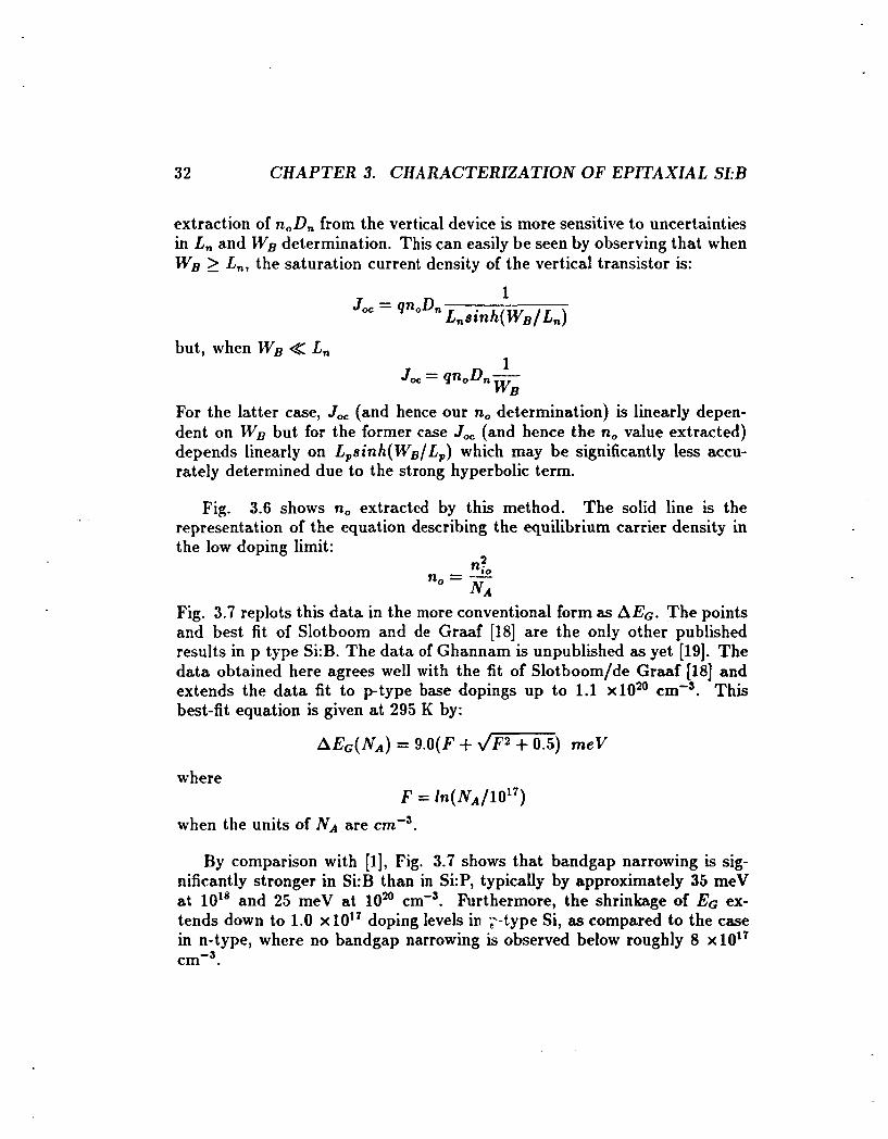
extraction of noDn from the vertical device is more sensitive to uncertainties in L, and W, determination. This can easily be seen by observing that when WE 2 L,, the saturation current density of the vertical transistor is:
1 Jm = qnoDn L,sinh(WB/L,)
but, when WB << L, i I J , = qn0Dn-
WB For the latter case, J , (and hence our no determination) is linearly depen- dent on W, but for the former case Joe (and hence the no value extracted) depends linearly on L,sinh( W B / L ~ ) which may be significantly less accu- rately determined due to the strong hyperbolic term.
Fig. 3.6 shows no extracted by this method. The solid line is the representation of the equation describing the equilibrium carrier density in the low doping limit:
. .
2 ni0 no = - N A
Fig. 3.7 replots this data in the more conventional form as AEG. The points and best fit of Slotboom and de Graaf [18] are the only other published results in p type Si:B. The data of Ghannam is unpublished as yet [19]. The data obtained here agrees well with the fit of Slotboom/de Graaf [18] and extends the data fit to p type base dopings up to 1.1 x10²⁰ ~ r n ' ~ . This best-fit equation is given a t 295 K by:
AEG(NA) = 9.O(F + dF2 + 0.5) meV
where
when the units of NA are crn-j.
F = /n(N~/10'')
By comparison with 111, Fig. 3.7 shows that bandgap narrowing is sig- nificantly stronger in Si:B than in Si:P, typically by approximately 35 meV at 10" and 25 meV a t lo2' ~ r n - ~ . Furthermore, the shrinkage of E G ex- tends down to 1.0 x10" doping levels in ;--type Si, as compared to the case in n-type, where no bandgap narrowing is observed below roughly 8 x1017 cm-'.

3.2. BANDGAP NARROWING IN P+ SI:B EPITAXIAL LAYERS 33
105,
T = 295 K n . (295 K) =9.565 lo9 ~ r n - ~
I
0 0
O I
ACCEPTOR DOPING N, ( ~ r n - ~ )
Figure 3.6: Equilibrium minority carrier density measured in different NA epitaxial Si:B layers.

34
9 E (3 z
Y
5 [r [r a Z a a (3 n z a m
2 w
t- Y U U w
w 0 a
CHAPTER 3. CHARACTERIZATION OF EPITAXIAL SI:B
120 i- o TH!S DATA (T=295 K) A SLOTBOOM/DEGRAAF o GHANNAM
40t P f / FIT OF SLOTBOOM.
201 i.’ I I I l l I 1 I l l I I I l l 1
1017 1018 1019 1020
ACCEPTOR DOPING N, (crn-3)
Figure 3.7: Effective bandgap narrowing as a fuction of acceptor doping NA.

Chapter 4
Conclusions
This report has summarized experimental measurements of the minority car- rier transport parameters in bulk heavily doped Si:B. Values and best fits of minority carrier mobility p,,, minority carrier lifetime T,, and effective bandgap narrowing A E G have been included. In addition, a characterization of the temperature and doping dependence of some majority carrier proper- ties of epitaxial Si:B has been given. The results are useful for modeling of heavily doped regions in bipolar semiconductor devices.
35
..
..

Bibliography
(11 J. A. del Alamo, S. E. Swirhun and R. M. Swanson, Simultaneous mea- surement of hole lifetime, hole mobility and bandgap narrowing in heav- ily doped n-type silicon, IEDM Tech. Digest, 1985, p. 290.
[2] J. A. del Alamo, S. E. Swirhun and R. M. Swanson, Measuring and modeling minority cari.ier transport in heavily doped silicon, Special Issue of Solid State Electonics, 28, p.47, 1985.
[3] J. A. del Alamo, PhD. dissertation, Dept. of EE, Stanford University, . .
November 1985.
[4] S. E. Swirhun, J. A. del Alamo and R. M. Swanson, Measurement of hole moblity in heavily doped n-type silicon, IEEE Electron Device Letts., 7,p. 168.,1986.
[5] S. M. Sze, Physics of Semiconductor Devices, John Wiley, 1981.
[6] R. A. Abram, G. J. Rees and B. L. H. Wilson, Heavily doped semicon- ductors and devices, Adv. Phys., 27, p. 799, 1978.
[7] J. D. Quirt and J. R. Marko, Absolute spin susceptibilities and other ESR parameters of heavily doped n-type silicon, 11; a unified treatment, Phys Rev. B, 7, p. 3842, 1973.
[8] J. F. Lin, S. S. Li, L. C. Linares and K. W. Teng, Theoretical analysis of hall factor and hall mobility in p t y p e silicon, Solid State Electronics, 24, p. 827, 1981.
36
..

..
BIBLIOGRAPHY 37
[9] W. R. Thurber, R. L. Mattis, Y. M. Liu and J. J. Filliben, The re- lationship between resistivity and dopant density for phosphorus and boron doped silicon, National Bureau of Standards publication NBS SP 400-64, May 1981.
[lo] J. Dziewior and W. Schmid, Auger coefficients for highly doped and
[ll] J. D. Beck and R. Conradt, Auger-rekomination in Si, Solid-state
[12] K. G. Svanteson, N. G. Nilsson and L. Huldt, Auger recombination in
[13] J. Dziewior and D. Silber, Minority carrier diffusion coefficients in highly doped silicon, Appl. Phys. Letts., 35, p. 170, 1979.
[14] H. S. Bennet, Hole and electron mobilities in heavily doped silicon: comparison of theory and experiments, Solid State Electronics, 26, p. 1157, 1983.
highly excited silicon, Appl. Physics Letts., 31, p. 346, 1977.
Comm., 13, p93, 1973.
silicon, Solid-state Comm., 11, p. 155, 1972.
[15] P. W. Chapman, 0. N. Tufte, J. D. Zook and D. Long, Electrical p r o p erties of heavily doped silicon, J. Appl. Physics, 34, p. 3291, 1963.
[16] K. Seeger, Semiconductor Physics, an Introduction, Second Edition,
I171 G. L. Pearson and J. Bardeen, Electrical properties of pure silicon and silicon alloys containing boron and phosphorus, Phys. Rev., 75, p. 865, 1949.
Springer Verlag, 1982.
[18] J . W. Slotboom and H. C. deGraaf, Measurements of bandgap narrowing in Si bipolar transistors, Solid State Electronics, 19, p. 857, 1976.
[19] M. Ghannam, PhD dissertation, Katholieke Universiteit Leuven, 1985.