department of ece - avniet
TRANSCRIPT

B MAMATHA
ASSISTANT PROFESSOR
AVNIET
1
ANALOG COMMMUNICATION
UNIT-I
DOUBLE SIDE BAND - SUPRESSED CARRIER
DEPARTMENT OF ECE

2
Contents
• Theory
• Implementation
– Transmitter
– Detector
• Synchronous
• Power analysis
• Summary

3
Double Side Band Suppressed Carrier
From AM spectrum:
• Carries signal c carries no information m.
• Carries signal consumes a lot of power more
than 50% c - m c c + m
Carrier
USB LSB
Single frequency Question: Why transmit carrier at all?
Ans:
Question: Can one suppress the carrier?
Ans.: Yes, just transmit two side bands (i.e DSB-SC)
System complexity at the receiver
But what is the penalty?

4
DSB-SC - Theory
General expression: )(cos])([)( 1 cctCtmktc
Let k1 = 1, C = 0 and c = 0, the modulated carrier signal, therefore:
ttmtc c cos)()(
Information signal m(t) = Em cos mt
Thus
tME
tME
ttEtc
mcc
mcc
cmm
)(cos2
)(cos2
coscos)(
upper side band lower side band

5
DSB-SC - Waveforms
B = 2m
Mixer
(Multiplier)
Notice: No carrier frequency

6
DSB-SC - Implementation
AM
mod.
Carrier
Ec cos ct
0.5 m(t)
-0.5 m(t)
+
-
DSB-SC
Ec m(t) cos ct
+
Ec (1+ 0.5 m(t) cos ct
Ec (1- 0.5 m(t) cos ct
• Balanced modulator
• Ring modulator
• Square-law modulator
AM
mod.

7
DSB-SC - Detection
• Synchronous detection
Multiplier Low pass filter Message signal
DSB-SC
Local oscillator
c(t) = cos ct tttmty cc cos]cos)([)(
ttmtm
ttmty
c
c
2cos)()(
]2cos1[)()(
21
21
21
)()(21 tmtv
Condition:
•Local oscillator has the same
frequency and phase as that of the
carrier signal at the transmitter.
m 2c+m 2c-m
Low pass filter
high frequency
information

8
DSB-SC - Synchronous Detection
• Case 1 - Phase error
Multiplier Low pass filter
Message signal DSB-SC
Local oscillator
c(t) = cos(ct+)
Condition:
•Local oscillator has the same
frequency but different phase
compared to carrier signal at the
transmitter.
m 2c+m 2c-m
Low pass filter
high frequency
information
)(cos]cos)([)( tttmty cc
)2(cos)(cos)(
)(cos)()2(cos)()(
21
21
21
21
ttmtm
tmttmty
c
c
cos)()(21 tmtv

9
Phase Synchronisation - Costas Loop
Recovered
signal
• When there is no phase error. The quadrature component is zero
• When 0, yip(t) decreases, while yqp(t) increases
X
VCO
DSB-SC
Ec cos (ct+)
LPF
Phase
discriminator
In-phase 0.5Ec m(t) cos
Vphase(t)
yip(t)
X. 0.5Ec m(t) sin
90o
phase shift
LPF
Ec sin (ct+)
Quadrature-phase yqp(t)
•The out put of the phase discriminator is proportional to

10
DSB-SC - Synchronous Detection
• Case 1 - Frequency error
Multiplier Low pass filter
Message signal DSB-SC
Local oscillator
c(t)=Eccos(ct+)
Condition:
•Local oscillator has the same
phase but different frequency
compared to carrier signal at the
transmitter.
m 2c+m 2c-m
Low pass filter
high frequency
information
)(cos]cos)([)( tttmty cc
)2(cos)(cos)(
)(cos)()2(cos)()(
21
21
21
21
ttmtm
tmttmty
c
c
cos)()(21 tmtv

11
DSB-SC - Power
• The total power (or average power):
R
ME
ME
RP
c
cSCDSBT
4
)(
2
2/2
2
2
• The maximum and peak envelop power
2)(
R
MEP c
SCDSBP

12
DSB-SC - Summary
• Advantages:
– Lower power consumption
• Disadvantage:
- Complex detection
• Applications:
- Analogue TV systems: to transmit colour information
- For transmitting stereo information in FM sound broadcast
at VHF

1
Department of ECE Sub: Analog Communications
Unit - 2
Single Side Band Suppressed Carrier
B MAMATHA
Assistant Professor
AVNIET

2
Content
• Theory
• Transmitter Implementation
• Detector Implementation
• Power Analysis
• Summary

3
Single Side Band Suppressed Carrier
From DSB-SC spectrum:
• Information m is carried twice
• Bandwidth is is high
c - m c c + m
Carrier
USB LSB
Single frequency Question: Why transmit both side bands?
Ans:
Question: Can one suppress one of the side bandcarrier?
Ans.: Yes, just transmit one side band (i.e SSB-SC)
System complexity at the receiver
But what is the penalty?

4
SSB-SC - Implementation
• Frequency discrimination
Multiplier Message
m(t)
Local oscillator
c(t) = cos ct
DSB-SC
tME
tME
ttEtc
mcc
mcc
cmm
)(cos2
)(cos2
coscos)(
Band pass filter c+ c
Band pass filter c- c
tME
tc mcc )(cos
2)(
tME
tc mcc )(cos
2)(
Upper sideband
Lower sideband

5
SSB-SC - Waveforms
B = 2m
USB
Bandwidth B = m
B = m

6
SSB-SC - Implementation cont.
• Phase discrimination (Hartley modulator)
X
SSB-SC
signal
X Em sin mt sin ct
sin ct
cos ct Carrier
90o
phase shift
Message m(t)
90o
phase shift
+
-
Em cos mt cos ct
Em sin mt
Em cos mt
v(t) =Em cos mt cos ct + Em sin mt sin
ct
= Em cos (m - c)t LSB
v(t) =Em cos mt cos ct - Em sin mt sin ct
= Em cos (m + c)t USB

7
SSB-SC - Hartley Modulator
• Advantages:
– No need for bulky and expensive band pass filters
– Easy to switch from a LSB to an USB SSB output
• Disadvantage:
– Requires Hilbert transform of the message signal. Hilbert
transform changes the phase of each +ve frequency
component by exactly - 90o.

8
SSB-SC - Detection
• Synchronous detection
Multiplier Low pass filter Message signal
SSB-SC
Local oscillator
c(t) = cos ct
Condition:
•Local oscillator has the same
frequency and phase as that of the
carrier signal at the transmitter.
m 2c+m
Low pass filter
high frequency
information
ttME
ty cmcc cos)(cos
2)(
tME
tME
ty mcc
mc )2(cos
4)(cos
4)(
tME
tv mc cos
4)(
9
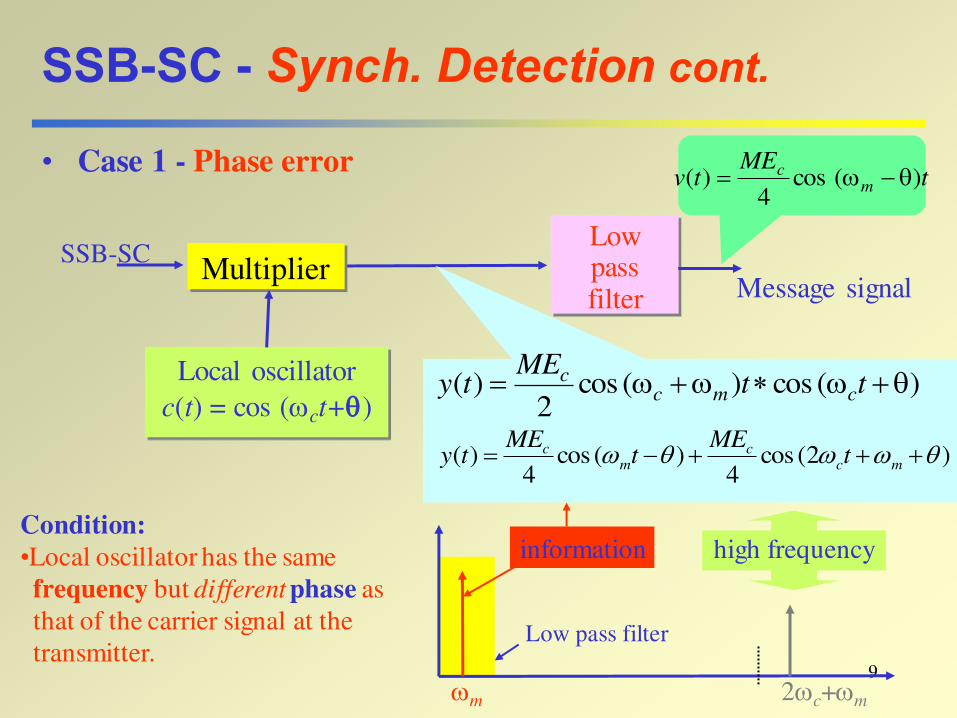
SSB-SC - Synch. Detection cont.
• Case 1 - Phase error
Multiplier Low pass filter Message signal
SSB-SC
Local oscillator
c(t) = cos (ct+)
Condition:
•Local oscillator has the same
frequency but different phase as
that of the carrier signal at the
transmitter.
m 2c+m
Low pass filter
high frequency
information
)(cos)(cos2
)( ttME
ty cmcc
)2(cos4
)(cos4
)( mcc
mc t
MEt
MEty
tME
tv mc )(cos
4)(

10
SSB-SC - Synch. Detection cont.
• Case 1 - Frequency error
Multiplier Low pass filter Message signal
SSB-SC
Local oscillator
c(t) = cos
(c+)t
Condition:
•Local oscillator has the same
phase but different frequency as
that of the carrier signal at the
transmitter.
m + 2c+m +
Low pass filter
high frequency
information
ttME
ty cmcc )(cos)(cos
2)(
tME
tME
ty mcc
mc )2(cos
4)(cos
4)(
tME
tv mc )(cos
4)(

11
SSB-SC - Power
• The total power (or average power):
R
ME
ME
RP
c
cSCSSBT
8
)(
2
2/1
2
2
• The maximum and peak envelop power
2
4
)(
R
MEP c
SCSSBP

12
SSB-SC - Summary
• Advantages: – Lower power consumption
– Better management of the frequency spectrum
– Less prone to selective fading
– Lower noise
• Disadvantage:
- Complex detection
• Applications:
- Two way radio communications
- Frequency division multiplexing
- Up conversion in numerous telecommunication systems

Department of ECE Sub: Analog Communicatons
Unit – 3 FREQUENCY MODULATION AND
DEMODULATION
B MAMTHA Assistant Professor
AVNIET

CONTENT:
Angle modulation vs. Amplitude modulation
FM Basics
Phase Modulation
Frequency Modulation
FM Characteristics
Relationship b/w FM & PM
Frequency Modulation
Narrow Band FM
WideBand FM
Bandwidth of FM
Phase Locked Loop
Advanatages, Disadvantages & Applications of FM

Angle Modulation vs. AM
Summarize: properties of amplitude modulation
– Amplitude modulation is linear
just move to new frequency band, spectrum shape does not change. No new frequencies generated.
– Spectrum: S(f) is a translated version of M(f)
– Bandwidth ≤ 2W
Properties of angle modulation
– They are nonlinear
spectrum shape does change, new frequencies generated.
– S(f) is not just a translated version of M(f)
– Bandwidth is usually much larger than 2W

FM Basics
VHF (30M-300M) high-fidelity broadcast
Wideband FM, (FM TV), narrow band FM (two-way radio)
1933 FM and angle modulation proposed by Armstrong, but success by 1949.
Digital: Frequency Shift Key (FSK), Phase Shift Key (BPSK, QPSK, 8PSK,…)
AM/FM: Transverse wave/Longitudinal wave

Instantaneous Frequency
( ) cos ( ) ,
where : carrier amplitude, ( ) : angle (phase)
c i
c i
s t A t
A t
( )1( )
2i
i
d tf t
dt
•Angle modulation has two forms - Frequency modulation (FM): message is represented as the variation of the instantaneous frequency of a carrier - Phase modulation (PM): message is represented as the variation of the instantaneous phase of a carrier
( ) cos 2 ( )c c
s t A f t t
where ( ) is a function of message signal ( ).t m t

Phase Modulation
PM (phase modulation) signal
( ) cos 2 ( )
c c ps t A f t k m t
( ) ( ), : phase sensitivity
( )instantanous frequency ( )
2
p p
p
i c
t k m t k
k dm tf t f
dt

Frequency Modulation
FM (frequency modulation) signal
0
( ) cos 2 2 ( )t
c c fs t A f t k m d
0
0
: frequency sensitivity
instantanous frequency ( ) ( )
angle ( ) 2 ( )
2 2 ( )
f
i c f
t
i i
t
c f
k
f t f k m t
t f d
f t k m d
(Assume zero initial phase)

FM Characteristics
Characteristics of FM signals
– Zero-crossings are not regular
– Envelope is constant
– FM and PM signals are similar

Relations between FM and PM
0FM of ( ) PM of ( )
t
m t m d
( )PM of ( ) FM of
dm tm t
dt


Frequency Modulation
FM (frequency modulation) signal
0
( ) cos 2 2 ( )t
c c fs t A f t k m d
0
0
: frequency sensitivity
instantanous frequency ( ) ( )
angle ( ) 2 ( )
2 2 ( )
f
i c f
t
i i
t
c f
k
f t f k m t
t f d
f t k m d
(Assume zero initial phase)
( ) cos(2 )m m
m t A f t cos(2 )i c f m m
f f k A f t
0
Let
2 cos(2 )21 1 1
2 2 2
1 2 cos(2 )
2
t
f m mc
i
c f m m t
d k A f dd f tdf
dt dt dt
f k A f

Example
m(t)
0 T 2T t
k and k
. T t for k)t( and
t0 for k)t(m k)t( isfrequency ousinstantane The
t.-T)-(t- d)m( d)m( d)m( , 1- m(t) T t for
and t d)m( , 1 m(t) t0 For 0.t at starts m(t) Assume
). d)m(ktcos( A )t(
fcmin ifcmax i
2T
fci
2T
fcfci
2T
2T
t
0
t
02T
t
02T
t
-
fcFM
2
T
2
T
t
)t(FM
Consider m(t)- a square wave- as shown. The FM wave for this m(t) is
shown below.

Frequency Deviation
Frequency deviation Δf
– difference between the maximum instantaneous and carrier frequency
– Definition:
– Relationship with instantaneous frequency
– Question: Is bandwidth of s(t) just 2Δf?
max | ( ) |f m f
f k A k m t
single-tone ( ) case: cos(2 )
general case:
i c m
c i c
m t f f f f t
f f f f f
No, instantaneous frequency is not
equivalent to spectrum frequency
(with non-zero power)!
S(t) has ∞ spectrum frequency (with non-zero power).
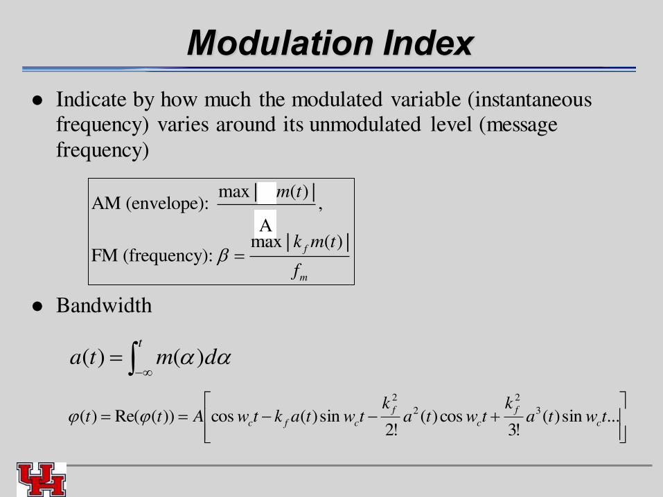
Modulation Index
Indicate by how much the modulated variable (instantaneous frequency) varies around its unmodulated level (message frequency)
Bandwidth
max | ( ) |AM (envelope): ,
1
max | ( ) |FM (frequency):
a
f
m
k m t
k m t
f
A
t
dmta )()(
...sin)(
!3cos)(
!2sin)(cos))(Re()( 3
2
2
2
twtak
twtak
twtaktwAtt c
f
c
f
cfc

Narrow Band Angle Modulation
1)( tak f
twtaktwAt cfc sin)(cos)( Definition
Equation
Comparison with AM Only phase difference of Pi/2 Frequency: similar Time: AM: frequency constant FM: amplitude constant
Conclusion: NBFM signal is
similar to AM signal NBFM has also bandwidth 2W. (twice message signal
bandwidth)


Block diagram of a method for generating a narrowband FM signal.

A phasor comparison of narrowband FM and AM waves for sinusoidal modulation. (a) Narrowband FM wave. (b) AM wave.

Wide Band FM
Wideband FM signal
Fourier series representation
( ) cos(2 )
( ) cos 2 sin(2 )
m m
c c m
m t A f t
s t A f t f t
( ) ( )cos 2 ( )
( ) ( ) ( ) ( )2
c n c m
n
c
n c m c m
n
s t A J f nf t
AS f J f f nf f f nf
( ) : -th order Bessel function of the first kindn
J n


Bessel Function of First Kind
0
1
2
1. ( ) ( 1) ( )
2. If is small, then ( ) 1,
( ) , 2
( ) 0 for all 2
3. ( ) 1
n
n n
n
n
n
J J
J
J
J n
J

Spectrum of WBFM (Chapter 5.2)
Spectrum when m(t) is single-tone
Example 2.2
( ) cos 2 sin(2 ) ( )cos 2 ( )
( ) ( ) ( ) ( )2
c c m c n c m
n
c
n c m c m
n
s t A f t f t A J f nf t
AS f J f f nf f f nf

Bandwidth of FM
Facts – FM has side frequencies extending to infinite frequency
theoretically infinite bandwidth
– But side frequencies become negligibly small beyond a point practically finite bandwidth
– FM signal bandwidth equals the required transmission (channel) bandwidth
Bandwidth of FM signal is approximately by
– Carson’s Rule (which gives lower-bound)

Carson’s Rule
Nearly all power lies within a bandwidth of
– For single-tone message signal with frequency fm
– For general message signal m(t) with bandwidth (or highest frequency) W
2 2 2( 1)T m m
B f f f
2 2 2( 1)T
B f W D W
where is deviation ratio (equivalent to ),
max ( )f
fD
W
f k m t

Phase-Locked Loop
Can be a whole course. The most important part of receiver.
Definition: a closed-loop feedback control system that generates and outputs a signal in relation to the frequency and phase of an input ("reference") signal
A phase-locked loop circuit responds both to the frequency and phase of the input signals, automatically raising or lowering the frequency of a controlled oscillator until it is matched to the reference in both frequency and phase.

Ideal Model
Model
– Si=Acos(wct+1(t)), Sv=Avcos(wct+c(t))
– Sp=0.5AAv[sin(2wct+1+c)+sin(1-c)]
– So=0.5AAvsin(1-c)=AAv(1-c)
Capture Range and Lock Range
LPF
VCO
Si
Sv
Sp So

Voltage Controlled Oscillator (VCO)
W(t)=wc+ce0(t), where wc is the free-running frequency
Example
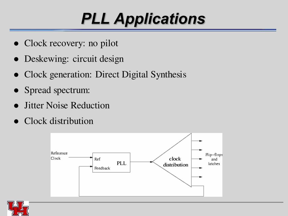
PLL Applications
Clock recovery: no pilot
Deskewing: circuit design
Clock generation: Direct Digital Synthesis
Spread spectrum:
Jitter Noise Reduction
Clock distribution

Angle Modulation Pro/Con Application
Why need angle modulation?
– Better noise reduction
– Improved system fidelity
Disadvantages
– Low bandwidth efficiency
– Complex implementations
Applications
– FM radio broadcast
– TV sound signal
– Two-way mobile radio
– Cellular radio
– Microwave and satellite communications

Department of ECE Sub: Analog Communications
Unit - 4 Effect of Noise on Analog Communication Systems
B MAMATHA
Assistant Professor
AVNIET

2
Content:
Effect of Noise on a Baseband System
Effect of Noise on DSB-SC AM
Effect of Noise on SSB-AM
Effect of Noise on Conventional AM

3
Introduction
Angle modulation systems and FM can provide a high degree of noise immunity
This noise immunity is obtained at the price of sacrificing channel bandwidth
Bandwidth requirements of angle modulation systems are considerably higher than that of amplitude modulation systems
This chapter deals with the followings: Effect of noise on amplitude modulation systems
Effect of noise on angle modulation systems
Carrier-phase estimation using a phase-locked loop (PLL)
Analyze the effects of transmission loss and noise on analog communication systems

4
Effect of Noise on a Baseband System
Since baseband systems serve as a basis for comparison of various modulation systems, we begin with a noise analysis of a baseband system.
In this case, there is no carrier demodulation to be performed.
The receiver consists only of an ideal lowpass filter with the bandwidth W.
The noise power at the output of the receiver, for a white noise input, is
If we denote the received power by PR, the baseband SNR is given by (6.1.2)
WNdfN
PW
Wn 0
0
20
WN
P
N
S R
b 0

5
White process
White process is processes in which all frequency components appear with equal power, i.e., the power spectral density (PSD), Sx(f), is a constant for all frequencies.
the PSD of thermal noise, Sn(f), is usually given as
(where k is Boltzrnann's constant and T is the temperature)
The value kT is usually denoted by N0, Then
2)( kTn fS
20)( N
n fS

6
Effect of Noise on DSB-SC AM
Transmitted signal :
The received signal at the output of the receiver noise-
limiting filter : Sum of this signal and filtered noise
Recall from Section 5.3.3 and 2.7 that a filtered noise process
can be expressed in terms of its in-phase and quadrature
components as
(where nc(t) is in-phase component and ns(t) is quadrature
component)
tftmAtu cc 2cos)()(
)2sin()()2cos()(
)2sin()(sin)()2cos()(cos)()](2cos[)()(
tftntftn
tfttAtfttAttftAtn
cscc
ccc

7
Effect of Noise on DSB-SC AM
Received signal (Adding the filtered noise to the
modulated signal)
Demodulate the received signal by first multiplying r(t)
by a locally generated sinusoid cos(2fct + ), where is
the phase of the sinusoid.
Then passing the product signal through an ideal
lowpass filter having a bandwidth W.
tftntftntftmA
tntutr
cscccc 2sin)(2cos)(2cos)(
)()()(

8
Effect of Noise on DSB-SC AM
The multiplication of r(t) with cos(2fct + ) yields
The lowpass filter rejects the double frequency components and
passes only the lowpass components.
tftntftntntn
tftmAtmA
tftftntftftn
tftftmA
tftntftu
tftr
csccsc
ccc
ccsccc
ccc
cc
c
4sin)(4cos)(sin)(cos)(
4cos)(cos)(
2cos2sin)(2cos2cos)(
2cos2cos)(
2cos)(2cos)(
2cos)(
21
21
21
21
sin)(cos)(cos)()( 21
21 tntntmAty scc

9
Effect of Noise on DSB-SC AM
In Chapter 3, the effect of a phase difference between the
received carrier and a locally generated carrier at the receiver is
a drop equal to cos2() in the received signal power.
Phase-locked loop (Section 6.4)
The effect of a phase-locked loop is to generate phase of the received carrier at the receiver.
If a phase-locked loop is employed, then = 0 and the demodulator is called a coherent or synchronous demodulator.
In our analysis in this section, we assume that we are employing a coherent demodulator. With this assumption, we assume that = 0
)()()( 2
1 tntmAty cc

10
Effect of Noise on DSB-SC AM
Therefore, at the receiver output, the message signal and the noise components are additive and we are able to define a meaningful SNR. The message signal power is given by
power PM is the content of the message signal
The noise power is given by
The power content of n(t) can be found by noting that it is the result of passing nw(t) through a filter with bandwidth Bc.
Mc
o PA
P4
2
nnn PPPc 4
1
4
10

11
Effect of Noise on DSB-SC AM Therefore, the power spectral density of n(t) is given by
The noise power is
Now we can find the output SNR as
In this case, the received signal power, given by Eq. (3.2.2), is
PR = Ac2PM /2.
otherwise
WfffS c
N
n0
||)( 2
0
00 24
2)( WNW
NdffSP nn
0
2
041
40
0 22
2
0WN
PA
WN
P
P
P
N
S McM
A
n
c

12
Effect of Noise on DSB-SC AM The output SNR for DSB-SC AM may be expressed as
which is identical to baseband SNR which is given by Equation (6.1.2).
In DSB-SC AM, the output SNR is the same as the SNR for a
baseband system
DSB-SC AM does not provide any SNR improvement over
a simple baseband communication system
WN
P
N
S R
DSB 00

13
Effect of Noise on SSB AM SSB modulated signal :
Input to the demodulator
Assumption : Demodulation with an ideal phase reference.
Hence, the output of the lowpass filter is the in-phase component (with a coefficient of ½) of the preceding signal.
)2sin()(ˆ)2cos()()( tftmAtftmAtu cccc
tftntmAtftntmA
tftntftntftmAtftmA
tntftmAtftmAtr
cscccc
cscccccc
cccc
2sin)()(ˆ)2cos()()(
2sin)(2cos)()2sin()(ˆ)2cos()(
)()2sin()(ˆ)2cos()()(
)()()( 21 tntmAty cc

14
Effect of Noise on SSB AM
Parallel to our discussion of DSB, we have
The signal-to-noise ratio in an SSB system is equivalent to that
of a DSB system.
0
20
0 0WN
PA
P
P
N
S Mc
n
McUR PAPP2
b
R
N
S
WN
P
N
S
SSB
00
Mc
o PA
P4
2
nnn PPPc 4
1
4
10
00 2
2)( WNW
NdffSP nn

15
Effect of Noise on Conventional AM
DSB AM signal :
Received signal at the input to the demodulator
a is the modulation index
mn(t) is normalized so that its minimum value is -1
If a synchronous demodulator is employed, the situation is basically
similar to the DSB case, except that we have 1 + amn(t) instead of m(t).
After mixing and lowpass filtering
)2cos()](1[)( tftamAtu cnc
tftntftntamA
tftntftntftamA
tntftamAtr
csccnc
cscccnc
cnc
2sin)()2cos()()](1[
2sin)(2cos)()2cos()](1[
)()2cos()](1[)(
)()()( 21 tntamAty cnc

16
Effect of Noise on Conventional AM Received signal power
Assumed that the message process is zero mean.
Now we can derive the output SNR as
denotes the modulation efficiency
Since , the SNR in conventional AM is always smaller than the SNR in a baseband system.
nM
cR Pa
AP
22
12
bbM
MR
M
M
M
A
M
MMc
n
Mc
N
S
N
S
Pa
Pa
WN
P
Pa
Pa
WN
Pa
Pa
Pa
WN
PaA
P
PaA
N
S
n
n
n
n
n
c
n
nn
c
n
AM
2
2
02
2
0
22
2
2
0
22
41
2241
0
11
1
12
2
nn MM PaPa22 1

17
Effect of Noise on Conventional AM In practical applications, the modulation index a is in the range of
0.8-0.9.
Power content of the normalized message process depends on the message source.
Speech signals : Large dynamic range, PM is about 0.1. The overall loss in SNR, when compared to a baseband system, is a
factor of 0.075 or equivalent to a loss of 11 dB.
The reason for this loss is that a large part of the transmitter power is used to send the carrier component of the modulated signal and not the desired signal.
To analyze the envelope-detector performance in the presence of
noise, we must use certain approximations.
This is a result of the nonlinear structure of an envelope detector,
which makes an exact analysis difficult.

18
Effect of Noise on Conventional AM
In this case, the demodulator detects the envelope of the
received signal and the noise process.
The input to the envelope detector is
Therefore, the envelope of r ( t ) is given by
Now we assume that the signal component in r ( t ) is much
stronger than the noise component. Then
Therefore, we have a high probability that
tftntftntamAtr csccnc 2sin)()2cos()()](1[)(
)()()](1[)( 22tntntamAtV scncr
1)](1[)( tamAtnP ncc
)()](1[)( tntamAtV cncr

19
Effect of Noise on Conventional AM
After removing the DC component, we obtain
which is basically the same as y(t) for the synchronous demodulation without the ½ coefficient.
This coefficient, of course, has no effect on the final SNR.
So we conclude that, under the assumption of high SNR
at the receiver input, the performance of synchronous
and envelope demodulators is the same.
However, if the preceding assumption is not true, that is, if we assume that, at the receiver input, the noise power is much
stronger than the signal power, Then
)()()( tntamAty cnc

20
Effect of Noise on Conventional AM
(a) : is small compared with the other components
(b) : ;the envelope of the noise process
Use the approximation
, where
)(1)(
)()(
)(1)(
)(1)(
)(1)()(
)(21)()(
)](1)[(2)()()](1[
)()()](1[)(
2
22
22
2222
22
tamtV
tnAtV
tamtV
tnAtV
tamtntn
tnAtntn
tamtnAtntntamA
tntntamAtV
n
n
ccn
n
n
ccn
b
n
sc
ccsc
a
nccscnc
scncr
22 )](1[ tamA nc
)()()( 22tVtntn nsc
smallfor,11 2 )(1)()(
)(222
tamtntn
tnAn
sc
cc

21
Effect of Noise on Conventional AM
Then
We observe that, at the demodulator output, the signal and the noise components are no longer additive.
In fact, the signal component is multiplied by noise and is no longer distinguishable.
In this case, no meaningful SNR can be defined.
We say that this system is operating below the threshold.
The subject of threshold and its effect on the performance of a communication system will be covered in more detail when we discuss the noise performance in angle modulation.
)(1)(
)()()( tam
tV
tnAtVtV n
n
ccnr

Department of ECE
Sub: Analog Communications
Unit - 5 PUSLE MODULATION TECHNIQUES
B MAMATHA
Assistant Professor
AVNIET

Content:
Pulse Amplitude Modulation
Pulse Width and Position Modulation
Demodulation of PWM & PPM

Pulse Amplitude Modulation – Natural and Flat-Top Sampling
The circuit of Figure 11-3 is used to illustrate pulse
amplitude modulation (PAM). The FET is the switch
used as a sampling gate.
When the FET is on, the analog voltage is shorted to
ground; when off, the FET is essentially open, so that
the analog signal sample appears at the output.
Op-amp 1 is a noninverting amplifier that isolates the
analog input channel from the switching function.

Figure 11-3. Pulse amplitude modulator, natural sampling.
Pulse Amplitude Modulation – Natural and Flat-Top Sampling

Op-amp 2 is a high input-impedance voltage follower
capable of driving low-impedance loads (high “fanout”).
The resistor R is used to limit the output current of op-
amp 1 when the FET is “on” and provides a voltage division with rd of the FET. (rd, the drain-to-source
resistance, is low but not zero)
Pulse Amplitude Modulation – Natural and Flat-Top Sampling

The most common technique for sampling voice in
PCM systems is to a sample-and-hold circuit.
As seen in Figure 11-4, the instantaneous amplitude of
the analog (voice) signal is held as a constant charge on
a capacitor for the duration of the sampling period Ts.
This technique is useful for holding the sample constant
while other processing is taking place, but it alters the
frequency spectrum and introduces an error, called
aperture error, resulting in an inability to recover
exactly the original analog signal.
Pulse Amplitude Modulation – Natural and Flat-Top Sampling

The amount of error depends on how mach the analog
changes during the holding time, called aperture time.
To estimate the maximum voltage error possible,
determine the maximum slope of the analog signal and
multiply it by the aperture time DT in Figure 11-4.
Pulse Amplitude Modulation – Natural and Flat-Top Sampling

Figure 11-4. Sample-and-hold circuit and flat-top sampling.
Pulse Amplitude Modulation – Natural and Flat-Top Sampling

Pulse Amplitude Modulation – Natural and Flat-Top Sampling
Figure 11-5. Flat-top PAM signals.

Recovering the original message signal m(t) from PAM signal
.completely recovered be can )( signal original eIdeally th
(3.20) )sin()sinc(
1
)(
1
is responseequalizer Let the
effect aparture
(3.19) )exp()sinc()(
by given is )( of ansformFourier tr
that theNote . )()( isoutput filter The
is bandwidthfilter theWhere
2delaydistortion amplitude
s
tm
f T
f
f TTfH
f Tjf TTfH
th
fHfMf
W
T
10

3.4 Other Forms of Pulse Modulation
a. Pulse-duration modulation (PDM)
b. Pulse-position modulation (PPM)
PPM has a similar noise performance as FM.
11

In pulse width modulation (PWM), the width of each pulse is made directly proportional to the amplitude of the information signal.
In pulse position modulation, constant-width pulses are used, and the position or time of occurrence of each pulse from some reference time is made directly proportional to the amplitude of the information signal.
PWM and PPM are compared and contrasted to PAM in Figure 11-11.
Pulse Width and Pulse Position Modulation

Figure 11-11. Analog/pulse modulation signals.
Pulse Width and Pulse Position Modulation

Figure 11-12 shows a PWM modulator. This circuit is simply a high-gain comparator that is switched on and off by the sawtooth waveform derived from a very stable-frequency oscillator.
Notice that the output will go to +Vcc the instant the analog signal exceeds the sawtooth voltage.
The output will go to -Vcc the instant the analog signal is less than the sawtooth voltage. With this circuit the average value of both inputs should be nearly the same.
This is easily achieved with equal value resistors to ground. Also the +V and –V values should not exceed Vcc.
Pulse Width and Pulse Position Modulation

Figure 11-12. Pulse width modulator.
Pulse Width and Pulse Position Modulation

A 710-type IC comparator can be used for positive-only output pulses that are also TTL compatible. PWM can also be produced by modulation of various voltage-controllable multivibrators.
One example is the popular 555 timer IC. Other (pulse output) VCOs, like the 566 and that of the 565 phase-locked loop IC, will produce PWM.
This points out the similarity of PWM to continuous analog FM. Indeed, PWM has the advantages of FM---constant amplitude and good noise immunity---and also its disadvantage---large bandwidth.
Pulse Width and Pulse Position Modulation

Since the width of each pulse in the PWM signal
shown in Figure 11-13 is directly proportional to the
amplitude of the modulating voltage.
The signal can be differentiated as shown in Figure
11-13 (to PPM in part a), then the positive pulses are
used to start a ramp, and the negative clock pulses
stop and reset the ramp.
This produces frequency-to-amplitude conversion (or
equivalently, pulse width-to-amplitude conversion).
The variable-amplitude ramp pulses are then time-
averaged (integrated) to recover the analog signal.
Demodulation

Figure 11-13. Pulse position modulator.
Pulse Width and Pulse Position Modulation

Demodulation
As illustrated in Figure 11-14, a narrow clock pulse sets an RS flip-flop output high, and the next PPM pulses resets the output to zero.
The resulting signal, PWM, has an average voltage proportional to the time difference between the PPM pulses and the reference clock pulses.
Time-averaging (integration) of the output produces the analog variations.
PPM has the same disadvantage as continuous analog phase modulation: a coherent clock reference signal is necessary for demodulation.
The reference pulses can be transmitted along with the PPM signal.
This is achieved by full-wave rectifying the PPM pulses of Figure 11-13a, which has the effect of reversing the polarity of the negative (clock-rate) pulses.
Then an edge-triggered flipflop (J-K or D-type) can be used to accomplish the same function as the RS flip-flop of Figure 11-14, using the clock input.
The penalty is: more pulses/second will require greater bandwidth, and the pulse width limit the pulse deviations for a given pulse period.
Demodulation

Figure 11-14. PPM demodulator.
Demodulation