demo mul dc2165a ltc3884 high efficiency, dual-output
TRANSCRIPT
1dc2165af
DEMO MANUAL DC2165A
DESCRIPTION
LTC3884EUK High Efficiency, Dual-Output, Synchronous Buck Converter
with Power System Management
Demonstration circuit 2165A is a high efficiency, high density, dual-output buck converter with a 4.5V to 14V input range. The output voltage is adjustable from 0.5V to 5.5V, and each output can supply up to 30A of load current when the output voltage is within a 0.5V to 1.8V range. This demo board features the LTC®3884, a dual-output poly phase step-down controller with ultra-low DCR sens-ing and incorporates digital power system management. The LTC3884 data sheet must be read in conjunction with this demo board manual for this demonstration circuit DC2165A.
The DC21065A powers up to default settings and pro-duces power based on configuration resistors or with its non-volatile memory without the need for any serial bus communication. This allows easy evaluation of the DC/DC converter. To fully explore the extensive power system management features of the part, download the
L, LT, LTC, LTM, Linear Technology and the Linear logo are registered trademarks and LTpowerPlay is a trademark of Linear Technology Corporation. All other trademarks are the property of their respective owners.
PERFORMANCE SUMMARY
GUI software LTpowerPlay™ onto your PC and use LTC’s I2C/SMBus/PMBus dongle DC1613A to connect to the board. LTpowerPlay allows the user to reconfigure the part on-the-fly and store the configuration in EEPROM, view telemetry of voltage, current, temperature and fault status.
GUI Software LTpowerPlay Download
The software can be downloaded from: http://www.linear.com/LTpowerPlay
For more details and instructions of LTpowerPlay, please refer to LTpowerPlay GUI for LTC3884 demo manual.
Design files for this circuit board are available at http://www.linear.com/demo/DC2165
Specifications are at TA = 25°C
PARAMETER CONDITIONS VALUE
Input Voltage Range 4.5V to 14V
Output Voltages, VOUT0/VOUT1 VIN = 4.5V to 14V, IOUT0/IOUT1 = 0A to 30A Default: 1V
Maximum Output Current, IOUT0/IOUT1 VIN = 4.5V to 14V, VOUT0/VOUT1 = 0.5V to 1.8V 30A
Typical Efficiency VIN = 12V, VOUT0/VOUT1 = 1.0V, IOUT0/IOUT1 = 30A 86.5%
Peak Efficiency VIN = 12V, VOUT0/VOUT1 = 1.0V 88.8%
Default Switching Frequency 425kHz

2dc2165af
DEMO MANUAL DC2165A
QUICK START PROCEDURE
Figure 1. Proper Measurement Equipment Setup
Demonstration circuit 2165A is easy to set up to evaluate the performance of the LTC3884. Refer to Figure 1 for the proper measurement equipment setup and follow the procedure below.
1. With power off, connect the input power supply to VIN (4.5V to 14V) and GND (input return).
2. Connect the output load between VOUT0/VOUT1 and GND (Initial load: no load).
3. Connect the DVMs to the input and outputs.
4. Check the default jumper/switch position: JP1: OFF, JP4: OFF, JP5: INT, SW1: OFF, SW2: OFF.
5. Turn on the input power supply up to 12V.
NOTE: Make sure that the input voltage does not exceed 14V.
6. Turn on the switches: SW1: ON, SW2: ON.
7. Check for the proper output voltages from VOUT0+ to VOUT0– and VOUT1+ to VOUT1–.
8. Once the proper output voltages are established, adjust the loads within the operating range and observe the output voltage regulation, ripple voltage and other parameters.
9. Connect the dongle and control the output voltages from the GUI. See LTpowerPlay Quick Start Guide session for details.
NOTE: When measuring the output or input voltage ripple, do not use the long ground lead on the oscil-loscope probe. See Figure 2 for the proper scope probe technique. Short, stiff leads need to be soldered to the (+) and (–) terminals of an output capacitor. The probe’s ground ring needs to touch the (–) lead and the probe tip needs to touch the (+) lead.
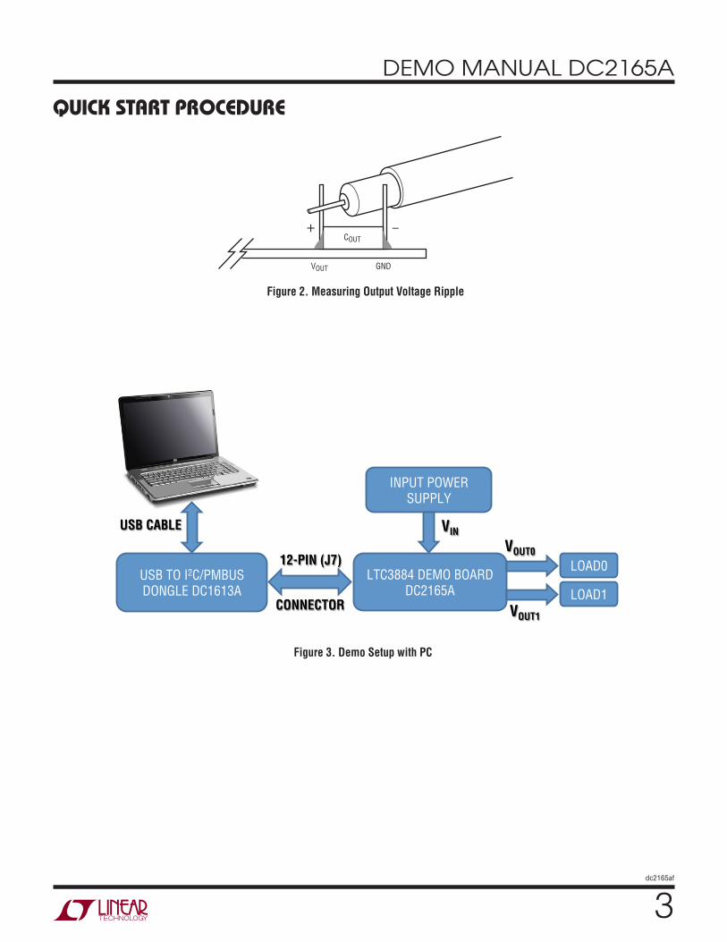
Connecting a PC to DC2165A
You can use a PC to reconfigure the power management features of the LTC3884 such as: nominal VOUT, margin set points, OV/UV limits, temperature fault limits, sequenc-ing parameters, the fault log, fault responses, GPIOs and other functionality. The DC2165A dongle may be plugged when VIN is present.
V
+
VIN 4.5V TO 14V
A
+ +
+
LOAD0 (30A)
1mΩ V
V +
VOUT0
+
LOAD1 (30A)
1mΩ
V
V +
VOUT1
3dc2165af
DEMO MANUAL DC2165A
+ –
VOUT GND
COUT
Figure 2. Measuring Output Voltage Ripple
Figure 3. Demo Setup with PC
QUICK START PROCEDURE
USB TO I2C/PMBUS DONGLE DC1613A
LTC3884 DEMO BOARD DC2165A
INPUT POWER SUPPLY
USB CABLE
12-PIN (J7)
CONNECTOR
LOAD0
LOAD1 VOUT1
VOUT0
VIN

4dc2165af
DEMO MANUAL DC2165A
Figure 4. Efficiency vs Load Current at VIN = 12V, fSW = 425kHz
OUTPUT LOAD CURRENT (A)0 5 10 15 20 25 30
75
80
85
90
95
EFFI
CIEN
CY (%
)
DC2165 F04
1.5VOUT1VOUT
VOUT0 (20MHz BW)(10mV/DIV)
Figure 5. Output Voltage Ripple at VIN = 12V, VOUT0 = 1V, IOUT0 = 30A
QUICK START PROCEDURE

5dc2165af
DEMO MANUAL DC2165A
Figure 6. Transient Response at VIN = 12V, VOUT0 = 1V, ∆IOUT0 = 7.5A
Figure 7. Thermal Performance at VIN = 12V, VOUT0 =1 .0V, IOUT0 = 30A, VOUT1 = 1.0V, IOUT1 = 30A, TA = 23.6°C, No Airflow
VOUT0 (20MHz BW)(20mV/DIV)
0A TO 7.5A LOAD STEP
QUICK START PROCEDURE

6dc2165af
DEMO MANUAL DC2165A
LTpowerPlay is a powerful Windows-based develop-ment environment that supports Linear Technology power system management ICs, including the LTM4676, LTC3880, LTC3883, LTC3884, LTC2974 and LTC2978. The software supports a variety of different tasks. You can use LTpowerPlay to evaluate Linear Technology ICs by connecting to a demo board system. LTpowerPlay can also be used in an offline mode (with no hardware pres-ent) in order to build a multichip configuration file that can be saved and reloaded at a later time. LTpowerPlay provides unprecedented diagnostic and debug features. It becomes a valuable diagnostic tool during board bring-up to program or tweak the power management scheme in a system, or to diagnose power issues when bringing up rails. LTpowerPlay utilizes the DC1613A USB-to-SMBus controller to communicate with one of many potential targets, including the LTM4676, the LTC3880, LTC3884
LTpowerPlay QUICK START GUIDE
Figure 8. LTpowerPlay Main Interface
and the LTC3883’s demo system, or a customer board. The software also provides an automatic update feature to keep the software current with the latest set of device drivers and documentation. The LTpowerPlay software can be downloaded from:
http://www.linear.com/LTpowerPlay
To access technical support documents for LTC Digital Power Products visit Help. View online help on the LTpowerPlay menu.
The following procedure describes how to use LTpowerPlay to monitor and change the settings of LTC3884.
1. Download and install the LTpowerPlay GUI:
http://www.linear.com/LTpowerPlay

7dc2165af
DEMO MANUAL DC2165A
2. Launch the LTpowerPlay GUI.
a. The GUI should automatically identify the DC2165A. The system tree on the left hand side should look like this:
LTpowerPlay QUICK START GUIDE
b. A green message box shows for a few seconds in the lower left hand corner, confirming that LTC3884 is communicating:
c. In the Toolbar, click the “R” (RAM to PC) icon to read the RAM from the LTC3884. This reads the configuration from the RAM of LTC3884 and loads it into the GUI.
d. If you want to change the output voltage to a different value, like 1.5V. In the Config tab, type in 1.5 in the VOUT_COMMAND box, like this:
Then, click the “W” (PC to RAM) icon to write these register values to the LTC3884. After finishing this step, you will see the output voltage will change to 1.5V.
8dc2165af
DEMO MANUAL DC2165A
If the write is successful, you will see the following message:
LTpowerPlay QUICK START GUIDE
PARTS LIST
e. You can save the changes into the NVM. In the tool bar, click “RAM to NVM” button, as following:
f. Save the demo board configuration to a (*.proj) file. Click the Save icon and save the file with a preferred file name.
ITEM QTY REFERENCE PART DESCRIPTION MANUFACTURER/PART NUMBER
Required Circuit Components
1 4 CIN1, CIN2, CIN3, CIN4 CAP, 1210 10μF 20% 35V X5R AVX 1210DD106MAT2A
2 10 COUT1, COUT2, COUT5, COUT6, COUT19, COUT20, COUT24, COUT25, C34, C35
CAP, 1210 100μF 20% 6.3V X5R AVX 12106D107MAT2A
3 8 COUT3, COUT4, COUT7, COUT8, COUT17, COUT18, COUT22, COUT23
CAP, 7343 330μF 20% 6.3V POSCAP PANASONIC 6TPF330M9L
4 5 C7, COUT21, COUT26, C41, C42 CAP, 0603 1μF 20% 25V X5R AVX 06033D105MAT2A
5 1 C1 CAP, 0603 2.2μF 20% 6.3V X5R AVX 06036D225MAT2A
6 2 C2, C32 CAP, 270μF 20% 16V OSCON PANASONIC 16SVPC270M
7 1 C3 CAP, 0805 1μF 10% 16V X7R AVX 0805YC105KAT2A
8 1 C4 CAP, 0603 4.7μF 10% 10V X5R AVX 0603ZD475KAT2A
0 1 C6 CAP, 0603 4.7μF 20% 25V X5R TDK C1608X5R1E475M080AC
10 2 C8, C15 CAP, 0603 0.1μF 10% 25V X7R AVX 06033C104KAT2A
11 2 C9, C16 CAP, 0603 220nF 10% 25V X7R TDK C1608X7R1E224K
12 3 C10, C12, C40 CAP, 0603 150pF 5% 50V NPO AVX 06035A151JAT2A
13 2 C11, C13 CAP, 0603 1500pF 5% 50V C0G MURATA GRM1885C1H152JA01D
14 4 C14, C17, C27, C28 CAP, 0603 10nF 10% 25V X7R AVX 06033C103KAT2A
15 2 C26, C39 CAP, 0603 100nF 20% 16V X7R AVX 0603YC104MAT2A
16 2 C30, C31 CAP, 1210 10μF 10% 16V X7R MURATA GRM32DR71C106KA01
17 2 D1, D2 DIODE, SCHOTTKY 30V, 100mA CENTRAL SEMI CMDSH-3-TR
18 4 D5, D6, D8, D9 LED, 0603 GREEN WURTH ELEKTRONIK 150060GS75000
19 1 D7 LED, 0603 RED WURTH ELEKTRONIK 150060SS75000
20 1 D12 DIODE, ULTRA LOW SCHOTTKY RECTIFIER NXP SEMI. PMEG2005AEL, 315
21 2 L1, L2 IND, 0.25μH WURTH ELEKTRONIK 744301025

9dc2165af
DEMO MANUAL DC2165A
ITEM QTY REFERENCE PART DESCRIPTION MANUFACTURER/PART NUMBER
22 2 Q1, Q5 XSTR, POWER MOSFET INFINEON BSC050NE2LS
23 2 Q3, Q8 XSTR, POWER MOSFET INFINEON BSC010NE2LSI
24 2 Q7, Q10 XSTR, PNP GENERAL PURPOSE DIODES INC. MMST3906-7-F
25 2 Q19, Q20 XSTR, N-CHANNEL DMOS FET DIODES INC. DMP3130L-7
26 4 Q21, Q22, Q25, Q26 XSTR, N-CHANNEL DMOS FET DIODES INC 2N7002A-7
27 2 Q23, Q24 XSTR, MOSFET, N-CHANNEL 30V VISHAY SUD50N04-8M8P-4GE3
28 1 R1 RES, 2512 0.005Ω 1% 1W SUSUMU KRL3264E-C-R005-F-T5
29 1 R2 RES, 0603 1Ω 1% 1/10W VISHAY CRCW06031R00FKEA
30 10 R3, R4, R15, R19, R63, R65, R66, R91, R113, R114
RES, 0603 0Ω JUMPER VISHAY CRCW06030000Z0EA
31 4 R5, R16, R18, R21 RES, 0603 10Ω 1% 1/10W VISHAY CRCW060310R0FKEA
32 12 R6, R7, R8, R10, R29, R30, R33, R34, R77, R87, R98, R105
RES, 0603 10kΩ 5% 1/10W VISHAY CRCW060310K0JNEA
33 6 R9, R11, R12, R13, R72, R73 RES, 0603 4.99kΩ 1% 1/10W VISHAY CRCW06034K99FKEA
34 2 R14, R20 RES, 0603 715Ω 1% 1/10W VISHAY CRCW0603715RFKEA
35 2 R69, R70 RES, 0603 10Ω 5% 1/10W VISHAY CRCW060310R0JNEA
36 1 R78 RES, 0603 15.8kΩ 1% 1/10W VISHAY CRCW060315K8FKEA
37 4 R79, R80, R125, R130 RES, 0603 200Ω 5% 1/10W VISHAY CRCW0603200RJNEA
38 1 R81 RES, 0603 127Ω 1% 1/10W VISHAY CRCW0603127RFKEA
39 1 R89 RES, 0603 2Ω 5% 1/10W VISHAY CRCW06032R00JNEA
40 1 R90 RES, 2010 0Ω JUMPER VISHAY CRCW20100000Z0EA
41 1 R92 RES, 0603 3.3Ω 1% 1/10W VISHAY CRCW06033R30FKEA
42 1 R93 RES, 0603 154kΩ 1% 1/10W VISHAY CRCW0603154KFKEA
43 1 R94 RES, 0603 1MΩ 5% 1/10W VISHAY CRCW06031M00JNEA
44 2 R95, R96 RES, 0603 20kΩ 5% 1/10W VISHAY CRCW060320K0JNEA
45 1 R97 RES, 0603 681kΩ 1% 1/10W VISHAY CRCW0603681KFKEA
46 1 R99 RES, 0603 182Ω 1% 1/10W VISHAY CRCW0603182RFKEA
47 1 R100 RES, 0603 82.5Ω 1% 1/10W VISHAY CRCW060382R5FKEA
48 1 R101 RES, 2512 0.01Ω 1% 1W VISHAY WSL2512R0100FEA
49 1 R103 RES, VARIABLE 5kΩ BOURNS 3386P-1-502-LF
50 1 R104 RES, 0603 649Ω 1% 1/10W VISHAY CRCW0603649RFKEA
51 1 R107 RES, 0603 34.8kΩ 1% 1/10W VISHAY CRCW060334K8FKEA
52 2 SW1, SW2 SWITCH, SUBMINIATURE SLIDE C&K JS202011CQN
53 1 U1 IC, LTC3884 LINEAR TECH. LTC3884EUK#10E1-1PBF-ES
54 1 U3 IC, 24LC05-I/ST MICROCHIP 24LC025-I/ST
55 1 U4 IC, REGULATOR LINEAR TECH. LT1761ES5-SD#PBF
56 1 U5 IC, LTC6992 LINEAR TECH. LTC6992IS6-1#PBF
57 1 U6 IC, SINGLE OP AMP LINEAR TECH. LT1803IS5#PBF
PARTS LIST

10dc2165af
DEMO MANUAL DC2165A
ITEM QTY REFERENCE PART DESCRIPTION MANUFACTURER/PART NUMBER
Additional Demo Board Circuit Components
1 0 C5 CAP, 0603 OPTION OPTION
2 0 D10, D11 DIODE, SCHOTTKY 30V, 100mA OPTION CENTRAL SEMI CMDSH-3-TR OPTION
3 0 Q2, Q4, Q6, Q9 XSTR, POWER MOSFET OPTION OPTION
4 0 R17, R22, R23, R24, R25, R26, R27, R28, R31, R32, R35, R36, R37, R38, R39, R40, R42, R43, R45, R46, R61, R62, R64, R67, R68, R74, R75, R106, R126, R139, R142, R146, R147
RES, 0603 OPTION OPTION
5 0 R41, R44, R47, R48, R85, R86, R88 RES, 2010 OPTION OPTION
6 0 R102 RES, 2512 OPTION OPTION
Hardware
1 26 E1, E2, E3, E4, E5, E6, E7, E8, E9, E10, E11, E12, E13, E14, E20, E21, E22, E23, E24, E25, E26, E27, E28, E29, E30, E31
TURRET MILL MAX 2501-2-00-80-00-00-07-0
2 3 JP1, JP4, JP5 HEADER, SINGLE ROW 3-PIN WURTH ELEKTRONIK 62000311131
3 6 J1, J2, J3, J4, J5, J6 STUD, TEST PIN PEM KFH-032-10
4 1 J7 HEADER, 12-PIN 2mm STR DL FCI 98414-G06-12ULF
5 1 J8 CONN, SOCKET 14-PIN DUAL ROW R/A SULLINS INC. NPPN072FJFN-RC
6 1 J9 HEADER, 14-PIN DUAL ROW R/A MOLEX 87760-1416
7 3 J10, J11, J12 CONN, BNC, 5 PINS AMPHENOL CONNEX 112404
8 1 J16 HEADER, 4-PIN 2mm STR DL HIROSE DF3A-4P-2DSA
9 7 LUG RING, #10 KEYSTONE 8205
10 14 NUT, BRASS 10-32 ANY #10-32
11 7 WASHER, #10 TIN PLATED BRASS ANY #10 EXT BZ TN
12 4 MH1, MH2, MH3, MH4 STANDOFF, SNAP ON KEYSTONE 8834
13 3 XJP1, XJP4, XJP5 SHUNT WURTH ELEKTRONIK, 60800213421
PARTS LIST

11dc2165af
DEMO MANUAL DC2165A
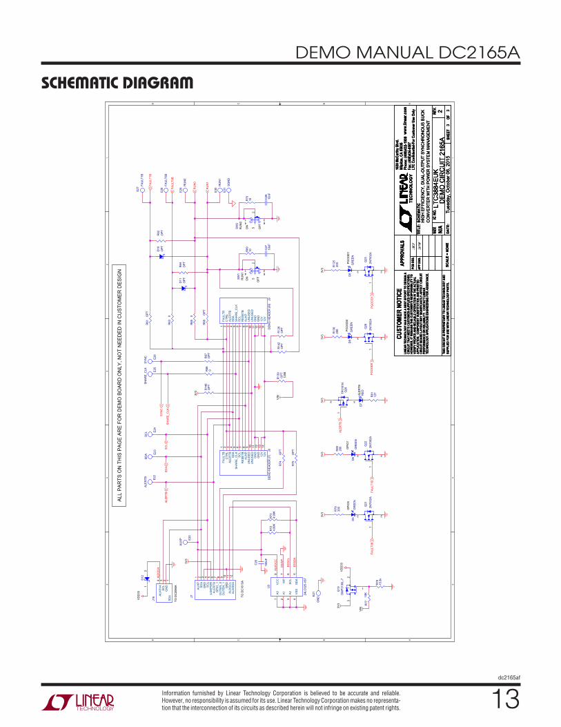
SCHEMATIC DIAGRAM5 5
4 4
3 3
2 2
1 1
DD
CC
BB
AA
NO
TE:
T1 -
T8 A
RE
EX
PO
SE
D P
CB
VIA
S
4.5V
- 14
V
1.0V
AT
30A
1.0V
AT
30A
WP
ON
OFF
7443
0102
5
7443
0102
5
OP
TIO
N F
OR
TW
O-P
HA
SE
CO
NFI
GU
RA
TIO
N C
ON
NE
CTI
ON
AS
EL0
AS
EL1
VO
UT0
_CFG
VO
UT1
_CFGSC
L
SD
A
ALE
RTB
FRE
Q_C
FG
PH
AS
E_C
FG
WP
1
SH
AR
E_C
LK
SY
NC
RU
N1
RU
N0
TSN
S1
TSN
S0
TG0
SW
0
BS
T0
BG
0
SW
1 BG
1
TG1
VIN
VD
D25
VO
UT1
VO
UT0
EX
TVC
CIN
TVC
CVD
D25
VD
D33
VIN
VIN
1
VIN
1
VD
D33
VIN
1
VIN
1
VD
D33
VD
D33
VD
D33
VD
D33
EX
TVC
C
INTV
CC
VD
D33
VD
D25
INTV
CC
INTV
CC
INTV
CC
SH
AR
E_C
LK
SY
NC
ALE
RTB
RU
N1
RU
N0
FAU
LT0B
FAU
LT1B
ITH
0
ITH
1
SC
L
SD
A
PG
OO
D0
VS
EN
SE
0+
VS
EN
SE
0-
VS
EN
SE
1+
VS
EN
SE
0-
VS
EN
SE
0+
VS
EN
SE
1+
VS
EN
SE
1-
PG
OO
D1
VS
EN
SE
1-
ITH
0IT
H1
RU
N0
RU
N1
FAU
LT0B
FAU
LT1B
VS
EN
SE
0+V
SE
NS
E1+
VS
EN
SE
0-V
SE
NS
E1-
PG
OO
D0
PG
OO
D1
VO
UT0
VO
UT1
SIZE
DATE
:
IC N
O.RE
V.
SHEE
TOF
TITL
E:
APPR
OVAL
S
PCB
DES.
APP
ENG.
TEC
HN
OLO
GY
Fax:
(408
)434
-050
7
Milp
itas,
CA 95
035
Phon
e: (4
08)4
32-1
900
1630
McC
arth
y Blvd
.
LTC
Conf
iden
tial-F
or C
usto
mer
Use
Onl
y
CUST
OMER
NOT
ICE
LINE
AR T
ECHN
OLOG
Y HA
S MA
DE A
BES
T EF
FORT
TO
DESI
GN A
CIRC
UIT
THAT
MEE
TS C
USTO
MER-
SUPP
LIED
SPE
CIFI
CATI
ONS;
HOW
EVER
, IT R
EMAI
NS T
HE C
USTO
MER'
S RE
SPON
SIBI
LITY
TO
VERI
FY P
ROPE
R AN
D RE
LIAB
LE O
PERA
TION
IN T
HE A
CTUA
LAP
PLIC
ATIO
N. C
OMPO
NENT
SUB
STIT
UTIO
N AN
D PR
INTE
DCI
RCUI
T BO
ARD
LAYO
UT M
AY S
IGNI
FICA
NTLY
AFF
ECT
CIRC
UIT
PERF
ORMA
NCE
OR R
ELIA
BILI
TY. C
ONTA
CT L
INEA
RTE
CHNO
LOGY
APP
LICA
TION
S EN
GINE
ERIN
G FO
R AS
SIST
ANCE
.
THIS
CIR
CUIT
IS P
ROPR
IETA
RY T
O LI
NEAR
TEC
HNOL
OGY
AND
SCHE
MAT
IC
SUPP
LIED
FOR
USE
WIT
H LI
NEAR
TEC
HNOL
OGY
PART
S.SC
ALE
= NO
NE
www.
linea
r.com 2
Tues
day,
Oct
ober
06,
201
51
3
HIG
H E
FFIC
IEN
CY
, DU
AL-
OU
TPU
T S
YN
CH
RO
NO
US
BU
CK
N/A
LTC
3884
EU
KD
EM
O C
IRC
UIT
216
5A
CO
NV
ER
TER
WIT
H P
OW
ER
SY
STE
M M
AN
AG
EM
EN
T
` \
[ j
RE
VIS
ION
HIS
TOR
YD
ES
CR
IPTI
ON
DA
TEA
PP
RO
VE
DE
CO
RE
V
[ j
PR
OTO
-2
04/2
2/15
RE
VIS
ION
HIS
TOR
YD
ES
CR
IPTI
ON
DA
TEA
PP
RO
VE
DE
CO
RE
V
[ j
PR
OTO
-2
04/2
2/15
RE
VIS
ION
HIS
TOR
YD
ES
CR
IPTI
ON
DA
TEA
PP
RO
VE
DE
CO
RE
V
[ j
PR
OTO
-2
04/2
2/15
E14
PG
OO
D1
J1
VIN
C8
0.1u
F
E9
EX
TVC
C
C7
1uF
R17
OP
T
C16
220n
F
JP1
1
2
3
E11
VD
D33
+C
OU
T833
0uF
6.3V
7343
C17
10nF
R11
40
R27
OP
T
Q5
BS
C05
0NE
2LS
3
12
4
5
Q4
OP
T
3
12
4
5
E4
VO
UT0
-
R23
OP
T
R37
OP
T
R15
0
R33
10K
R21 10 1%
R36
OP
T
R11
4.99
K
J2
GN
D
R6
10K
C1
2.2u
F
E13
PG
OO
D0
C11
1500
pF
C3
1uF
0805
Q9
OP
T
3
12
4
5
E5
VO
UT1
+
C10
150p
F
CO
UT6
100u
F
1210
6.3V
R47
OP
T
2010
R14
7O
PT
Q3
BS
C01
0NE
2LS
I
3
12
4
5
C6
4.7u
F
E12
VD
D25
J6
GN
D
L10.
25uH
C5 OP
TQ
2O
PT
3
12
4
5
CO
UT5
100u
F
1210
6.3V
R24
OP
T
R2
11%
R12 4.99
K
Q8
BS
C01
0NE
2LS
I
3
12
4
5
R45
OP
T
E3
VO
UT0
+
R3 0
J5
VO
UT1
R29
10K
R8
10K
C13
1500
pF
R19
0
R20
715
1%
J3
VO
UT0
R11
30
CIN
410
uF12
10
CIN
210
uF12
10
R46
OP
T
Q6
OP
T
3
12
4
5
D1
CM
DS
H-3
-TR
R34
10K
+C
OU
T333
0uF
6.3V
7343
R32
OP
TR
31O
PT
R9
4.99
K
Q7
MM
BT3
906-
AL3
-RS
OT-
323
R30
10K
E1
VIN
+
R44
OP
T
2010
R18
10 1%
R35
OP
T
E6
VO
UT1
-
D2
CM
DS
H-3
-TR
+C
OU
T433
0uF
6.3V
7343
C12
150p
F
L20.
25uH
E10
INTV
CC
R22
OP
T
Q1
BS
C05
0NE
2LS
3
12
4
5
R4
0
Q10
MM
BT3
906-
AL3
-RS
OT-
323
+C
3227
0uF
16V
J4
GN
D
U1
LTC
3884
EU
K
TG1
35
SW1
34
BOO
ST1
36IIN-
47
PGND41
BOO
ST0
43SW
045
ITH
_R0
5
SYN
C11
SCL
12
SDA
13
ALER
TB14
SHAR
E_C
LK27
RU
N0
17
RU
N1
18
ITH
_R1
30
ITH
129
TSN
S010
TSN
S19
ASEL
019
ASEL
120
VDD3328
ITH
06
WP
26
VDD2525
IIN+46
FAU
LT0B
15
FAU
LT1B
16
BG1
37
ISEN
SE1+
3
VOU
T1_C
FG22
VSEN
SE1-
31VS
ENSE
1+32
ISEN
SE1-
4
VSEN
SE0+
1IS
ENSE
0-8
ISEN
SE0+
7
BG0
42
VOU
T0_C
FG21
VSEN
SE0-
2
49GND
FREQ
_CFG
23
PHAS
E_C
FG24
PGOOD133
PGOOD048
TG0
44
INTVCC38
VIN39
EXTV
CC
40R
1010
KR
134.
99K
C15
0.1u
F
R7
10K
R25
OP
T
CIN
310
uF12
10
R43
OP
T
R39
OP
T
C9
220n
F
E2
VIN
-
R28
OP
T
R42
OP
T
R41
OP
T
2010
CIN
110
uF12
10
C4
4.7u
F
+C
227
0uF
16V
R40
OP
T
R48
OP
T
2010
R16
10
CO
UT1
100u
F
1210
6.3V
R14
715
1%
R38
OP
T
CO
UT2
100u
F
1210
6.3V
C14
10nF
+C
OU
T733
0uF
6.3V
7343
R26
OP
T
R1
0.00
525
12
R5
10
12dc2165af
DEMO MANUAL DC2165A
SCHEMATIC DIAGRAM5 5
4 4
3 3
2 2
1 1
DD
CC
BB
AA
VO
UT0
VO
UT1
PU
LSE
DY
NA
MIC
LO
AD
TE
ST
CIR
CU
IT, F
OR
DE
MO
BO
AR
D O
NLY
70H
z, 3
% D
uty
Cyc
le
INT
EX
T
1% 1%
IOU
T S
TEP
OP
TIO
NA
L 5.
5V B
IAS
OP
T20
1020
10O
PT
BLE
ED
ER
LO
AD
S
ON
OFF
BIA
S
+5.5
V
EX
TVC
C
VIN
+5.5
V
VO
UT0
VO
UT1
VO
UT0
VO
UT1
SIZE
DATE
:
IC N
O.RE
V.
SHEE
TOF
TITL
E:
APPR
OVAL
S
PCB
DES.
APP
ENG.
TEC
HN
OLO
GY
Fax:
(408
)434
-050
7
Milp
itas,
CA 95
035
Phon
e: (4
08)4
32-1
900
1630
McC
arth
y Blvd
.
LTC
Conf
iden
tial-F
or C
usto
mer
Use
Onl
y
CUST
OMER
NOT
ICE
LINE
AR T
ECHN
OLOG
Y HA
S MA
DE A
BES
T EF
FORT
TO
DESI
GN A
CIRC
UIT
THAT
MEE
TS C
USTO
MER-
SUPP
LIED
SPE
CIFI
CATI
ONS;
HOW
EVER
, IT R
EMAI
NS T
HE C
USTO
MER'
S RE
SPON
SIBI
LITY
TO
VERI
FY P
ROPE
R AN
D RE
LIAB
LE O
PERA
TION
IN T
HE A
CTUA
LAP
PLIC
ATIO
N. C
OMPO
NENT
SUB
STIT
UTIO
N AN
D PR
INTE
DCI
RCUI
T BO
ARD
LAYO
UT M
AY S
IGNI
FICA
NTLY
AFF
ECT
CIRC
UIT
PERF
ORMA
NCE
OR R
ELIA
BILI
TY. C
ONTA
CT L
INEA
RTE
CHNO
LOGY
APP
LICA
TION
S EN
GINE
ERIN
G FO
R AS
SIST
ANCE
.
THIS
CIR
CUIT
IS P
ROPR
IETA
RY T
O LI
NEAR
TEC
HNOL
OGY
AND
SCHE
MAT
IC
SUPP
LIED
FOR
USE
WIT
H LI
NEAR
TEC
HNOL
OGY
PART
S.SC
ALE
= NO
NE
www.
linea
r.com 2
Frid
ay, S
epte
mbe
r 04,
201
52
3
HIG
H E
FFIC
IEN
CY
, DU
AL-
OU
TPU
T S
YN
CH
RO
NO
US
BU
CK
N/A
LTC
3884
EU
KD
EM
O C
IRC
UIT
216
5A
CO
NV
ER
TER
WIT
H P
OW
ER
SY
STE
M M
AN
AG
EM
EN
T
[ j
` \
R98 10
K
C42
1.0u
F
Q24
SU
D50
N04
-8M
8P-4
GE
3
C30
10uF
16V
1210
R10
10.
0125
12
E7E
XT
PU
LSE
R10
35K
CO
UT2
11.
0uF
R99 182
J10
1
2
R10
0
82.5
1%
C41
1.0u
F
+C
OU
T17
330u
F6.
3V73
43
R10
734
.8K
1%
R10
464
9
R93
154k
1%
R10
2O
PT
2512
+C
OU
T22
330u
F6.
3V73
43
+C
OU
T18
330u
F6.
3V73
43
CO
UT2
61.
0uF
R94
1MU
6LT
1803
IS5
VO
UT
1
V-
2
+IN
3-IN
4
V+
5
+C
OU
T23
330u
F6.
3V73
43
C40
150p
F
U4
LT17
61E
S5-
SD
IN1
AD
J4
SH
DN
3G
ND
2O
UT
5
R96
20K
E8
GN
D
C39
100n
F
C31
10uF
16V
1210
U5
LTC
6992
IS6-
1
MO
D1
GN
D2
SE
T3
DIV
4V
+5
OU
T6
R87
10K
C35
100u
F
1210
6.3V
R88
OP
T
2010
J11
1
2
C34
100u
F
1210
6.3V
R91
0
R10
510
K
R97
681K
1%
R89
2
CO
UT2
510
0uF
1210
6.3V
R90
0
2010
R85
CO
UT2
010
0uF
1210
6.3V
JP4
1
2
3J1
21
2
Q23
SU
D50
N04
-8M
8P-4
GE
3
JP5
1
2
3
CO
UT2
410
0uF
1210
6.3V
R10
6
OP
T
CO
UT1
910
0uF
1210
6.3V
R92
3.3
1%
R95
20K
R86
13dc2165af
DEMO MANUAL DC2165A
Information furnished by Linear Technology Corporation is believed to be accurate and reliable. However, no responsibility is assumed for its use. Linear Technology Corporation makes no representa-tion that the interconnection of its circuits as described herein will not infringe on existing patent rights.
SCHEMATIC DIAGRAM5 5
4 4
3 3
2 2
1 1
DD
CC
BB
AA
ALL
PA
RTS
ON
TH
IS P
AG
E A
RE
FO
R D
EM
O B
OA
RD
ON
LY, N
OT
NE
ED
ED
IN C
US
TOM
ER
DE
SIG
N
PGO
OD
0PG
OO
D1
TO D
C20
86A
ON
OFF
ON
OFF
RU
N0
RU
N1
TO D
C16
13A
1206
GPI
O0
GPI
O1
ALER
TB
EEW
P
EESD
A
AUX3
V4 AUXV
CC
EESC
L
3V3
3V3
VDD
33
3V3
VIN3V
3
VIN3V
3
VDD
33
3V3
3V3
3V3
PGO
OD
1PG
OO
D0
ALER
TBSD
ASC
L
RU
N0
RU
N1
FAU
LT1B
FAU
LT0B
SYN
C
SHAR
E_C
LK
FAU
LT0B
FAU
LT1B
ALER
TB
SIZE
DATE
:
IC N
O.RE
V.
SHEE
TOF
TITL
E:
APPR
OVAL
S
PCB
DES.
APP
ENG.
TEC
HN
OLO
GY
Fax:
(408
)434
-050
7
Milp
itas,
CA 95
035
Phon
e: (4
08)4
32-1
900
1630
McC
arth
y Blvd
.
LTC
Conf
iden
tial-F
or C
usto
mer
Use
Onl
y
CUST
OMER
NOT
ICE
LINE
AR T
ECHN
OLOG
Y HA
S MA
DE A
BES
T EF
FORT
TO
DESI
GN A
CIRC
UIT
THAT
MEE
TS C
USTO
MER-
SUPP
LIED
SPE
CIFI
CATI
ONS;
HOW
EVER
, IT R
EMAI
NS T
HE C
USTO
MER'
S RE
SPON
SIBI
LITY
TO
VERI
FY P
ROPE
R AN
D RE
LIAB
LE O
PERA
TION
IN T
HE A
CTUA
LAP
PLIC
ATIO
N. C
OMPO
NENT
SUB
STIT
UTIO
N AN
D PR
INTE
DCI
RCUI
T BO
ARD
LAYO
UT M
AY S
IGNI
FICA
NTLY
AFF
ECT
CIRC
UIT
PERF
ORMA
NCE
OR R
ELIA
BILI
TY. C
ONTA
CT L
INEA
RTE
CHNO
LOGY
APP
LICA
TION
S EN
GINE
ERIN
G FO
R AS
SIST
ANCE
.
THIS
CIR
CUIT
IS P
ROPR
IETA
RY T
O LI
NEAR
TEC
HNOL
OGY
AND
SCHE
MAT
IC
SUPP
LIED
FOR
USE
WIT
H LI
NEAR
TEC
HNOL
OGY
PART
S.SC
ALE
= NO
NE
www.
linea
r.com 2
Tues
day,
Oct
ober
06,
201
53
3
HIG
H E
FFIC
IEN
CY
, DU
AL-
OU
TPU
T S
YN
CH
RO
NO
US
BU
CK
`\
N/A
LTC
3884
EU
KD
EM
O C
IRC
UIT
216
5A
CO
NV
ER
TER
WIT
H P
OW
ER
SY
STE
M M
AN
AG
EM
EN
T
[ j
E29
RU
N0
J7
AU
XP
1
SD
A2
GN
D3
SC
L4
LGK
PW
R5
ALE
RTB
6
GP
IO_1
7
OU
TEN
_08
OU
TEN
_19
GN
D10
AU
XS
CL
11
AU
XS
DA
12
R61
OPT
R13
020
0
R69
10
R74
OPT
R73
4.99
K R79
200
J8D
EMO
HEA
DER
(F)
FAU
LTB
1
CTR
L2
ALE
RTB
3
SD
A4
SH
AR
E_C
LK5
SC
L6
RE
SE
TB7
AU
XP
8
UN
US
ED
9
UN
US
ED
10
GN
D11
GN
D12
12V
13
12V
14
R13
9O
PT
D10
OP
T
E30
RU
N1
R77
10K
Q25
2N70
02A
23
1
Q19
DM
P313
0L-7
23
1
Q20
TP01
01K
2 3
1
SW1
1
2
34
5
6
D11
OP
T
U3
24LC
025-
I/ST
A0
1
A1
2
A2
3
VS
S4
SD
A5
SC
L6
WP
7V
CC
8
D7
RED
Q26
2N70
02A
23
1
C28
10nF
Q21
2N70
02A
23
1
R14
2O
PT
J16 A
UX
3V4
4
SC
L3
GN
D2 1
SDA
R12
6O
PT
R81
127
R78
15.8
k
Q22
2N70
02A
23
1
R66 0
E22
ALER
TB
E27
FAU
LT1B
J9D
EMO
HEA
DER
(M)
FAU
LTB
1
CTR
L2
ALE
RTB
3
SD
A4
SH
AR
E_C
LK5
SC
L6
RE
SE
TB7
AU
XP
8
UN
US
ED
9
UN
US
ED
10
GN
D11
GN
D12
12V
13
12V
14
R67
OPT
E24
SCL
D12
21
R72
4.99
K
E28
FAU
LT0B
SW2
1
2
34
5
6
C26
100n
F
D6
GR
EEN
R14
6O
PT
E25
SHAR
E_C
LK
R62
OPT
R80
200
R68
OPT
E20
AUXP
D8
GR
EEN
E26
SYN
C
C27
10nF
R75
OPT
R64
OPT
D5
GR
EEN
D9
GR
EEN
E23
SDA
R63
0
E21
GN
D
R70
10
R65
0
E31
SGN
D
R12
520
0
14dc2165af
DEMO MANUAL DC2165A
Linear Technology Corporation1630 McCarthy Blvd., Milpitas, CA 95035-7417 (408) 432-1900 FAX: (408) 434-0507 www.linear.com LINEAR TECHNOLOGY CORPORATION 2015
LT 1215 • PRINTED IN USA
DEMONSTRATION BOARD IMPORTANT NOTICE
Linear Technology Corporation (LTC) provides the enclosed product(s) under the following AS IS conditions:
This demonstration board (DEMO BOARD) kit being sold or provided by Linear Technology is intended for use for ENGINEERING DEVELOPMENT OR EVALUATION PURPOSES ONLY and is not provided by LTC for commercial use. As such, the DEMO BOARD herein may not be complete in terms of required design-, marketing-, and/or manufacturing-related protective considerations, including but not limited to product safety measures typically found in finished commercial goods. As a prototype, this product does not fall within the scope of the European Union directive on electromagnetic compatibility and therefore may or may not meet the technical requirements of the directive, or other regulations.
If this evaluation kit does not meet the specifications recited in the DEMO BOARD manual the kit may be returned within 30 days from the date of delivery for a full refund. THE FOREGOING WARRANTY IS THE EXCLUSIVE WARRANTY MADE BY THE SELLER TO BUYER AND IS IN LIEU OF ALL OTHER WARRANTIES, EXPRESSED, IMPLIED, OR STATUTORY, INCLUDING ANY WARRANTY OF MERCHANTABILITY OR FITNESS FOR ANY PARTICULAR PURPOSE. EXCEPT TO THE EXTENT OF THIS INDEMNITY, NEITHER PARTY SHALL BE LIABLE TO THE OTHER FOR ANY INDIRECT, SPECIAL, INCIDENTAL, OR CONSEQUENTIAL DAMAGES.
The user assumes all responsibility and liability for proper and safe handling of the goods. Further, the user releases LTC from all claims arising from the handling or use of the goods. Due to the open construction of the product, it is the user’s responsibility to take any and all appropriate precautions with regard to electrostatic discharge. Also be aware that the products herein may not be regulatory compliant or agency certified (FCC, UL, CE, etc.).
No License is granted under any patent right or other intellectual property whatsoever. LTC assumes no liability for applications assistance, customer product design, software performance, or infringement of patents or any other intellectual property rights of any kind.
LTC currently services a variety of customers for products around the world, and therefore this transaction is not exclusive.
Please read the DEMO BOARD manual prior to handling the product. Persons handling this product must have electronics training and observe good laboratory practice standards. Common sense is encouraged.
This notice contains important safety information about temperatures and voltages. For further safety concerns, please contact a LTC application engineer.
Mailing Address:
Linear Technology
1630 McCarthy Blvd.
Milpitas, CA 95035
Copyright © 2004, Linear Technology Corporation