deformation theory
DESCRIPTION
deformation theoryTRANSCRIPT
1
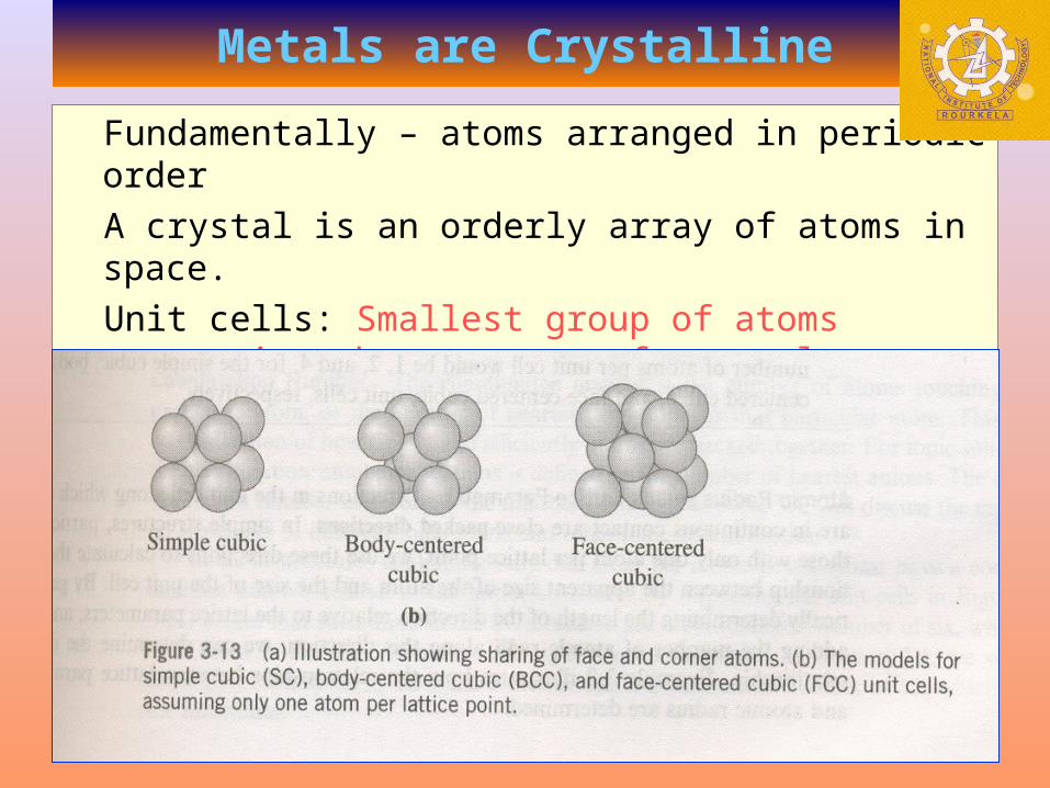
Metals are Crystalline
Fundamentally – atoms arranged in periodic order
A crystal is an orderly array of atoms in space.
Unit cells: Smallest group of atoms possessing the symmetry of crystal
Most metals crystallize: bcc, fcc & hcp
2
Real crystals deviate from perfect periodicity and known as lattice defects.Defects affect Physical & Mechanical Properties
Structure sensitive and insensitive properties• Structure sensitive - Mechanical Properties• Structure insensitive - Physical Properties
Lattice Defects

3
Slip planes/ directions in bcc
4
Contd… lattice defects
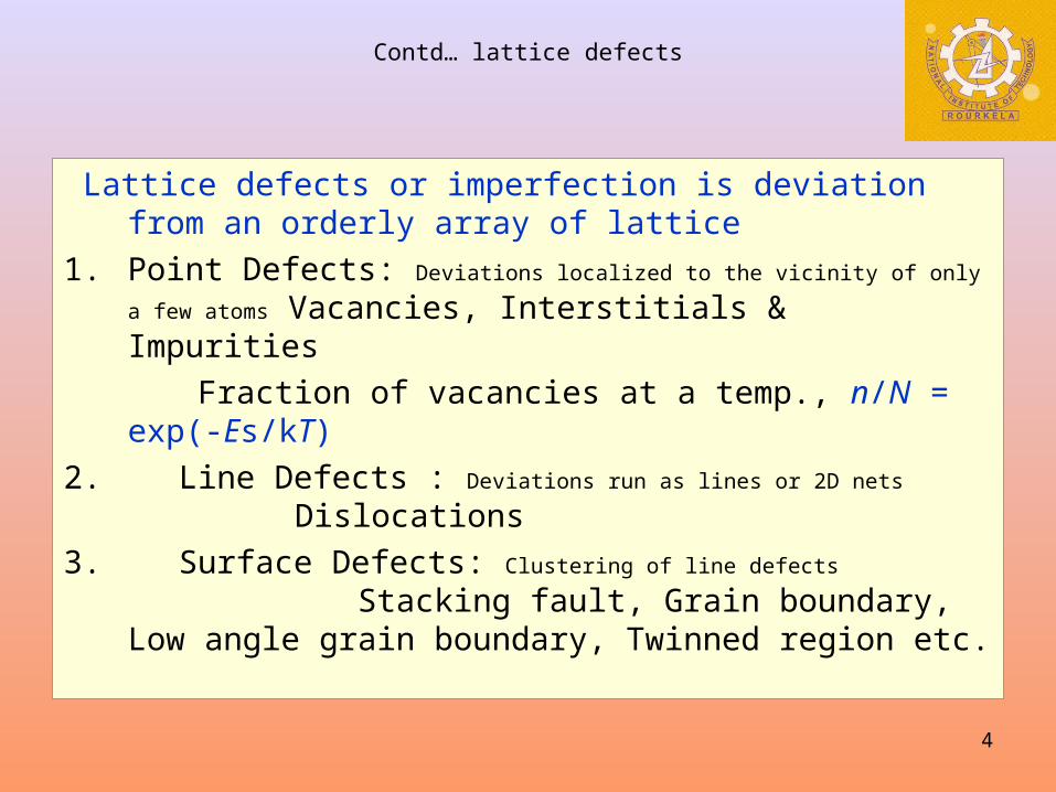
Lattice defects or imperfection is deviation from an orderly array of lattice
1. Point Defects: Deviations localized to the vicinity of only a few atoms Vacancies, Interstitials & Impurities
Fraction of vacancies at a temp., n/N = exp(-Es/kT)
2. Line Defects : Deviations run as lines or 2D nets
Dislocations
3. Surface Defects: Clustering of line defects Stacking fault, Grain boundary, Low angle grain boundary, Twinned region etc.
5
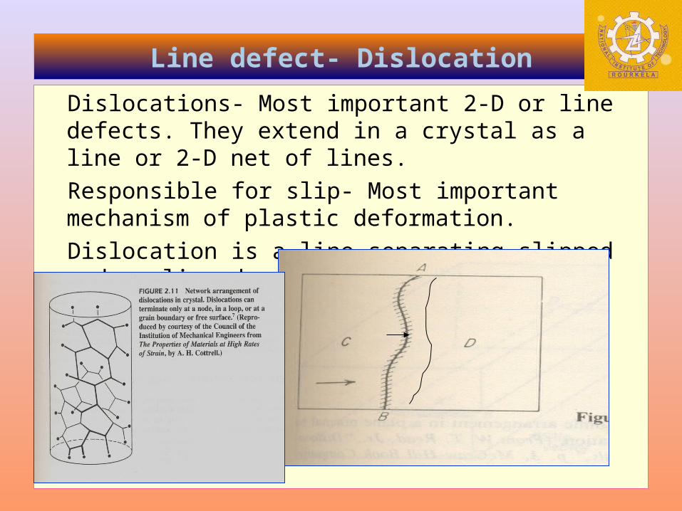
Dislocations- Most important 2-D or line defects. They extend in a crystal as a line or 2-D net of lines.
Responsible for slip- Most important mechanism of plastic deformation.
Dislocation is a line separating slipped and unslipped region of a crystal.
Line defect- Dislocation
6
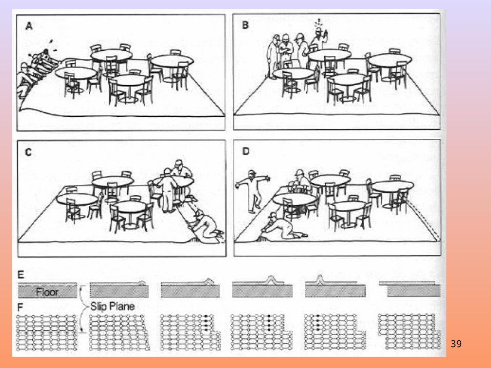
The usual method of plastic deformation is slip. This is sliding of one block of crystal over other block. Slip is responsible for plastic deformation and deferent mechanisms of mechanical behaviour.
This takes place along a definite crystallographic plane (slip plane).
Crude approximation, it is like distortion produced in a deck of cards when pushed from one end.
Slip in a crystal can be understood with the help of the Fig.1
Deformation by Slip
7
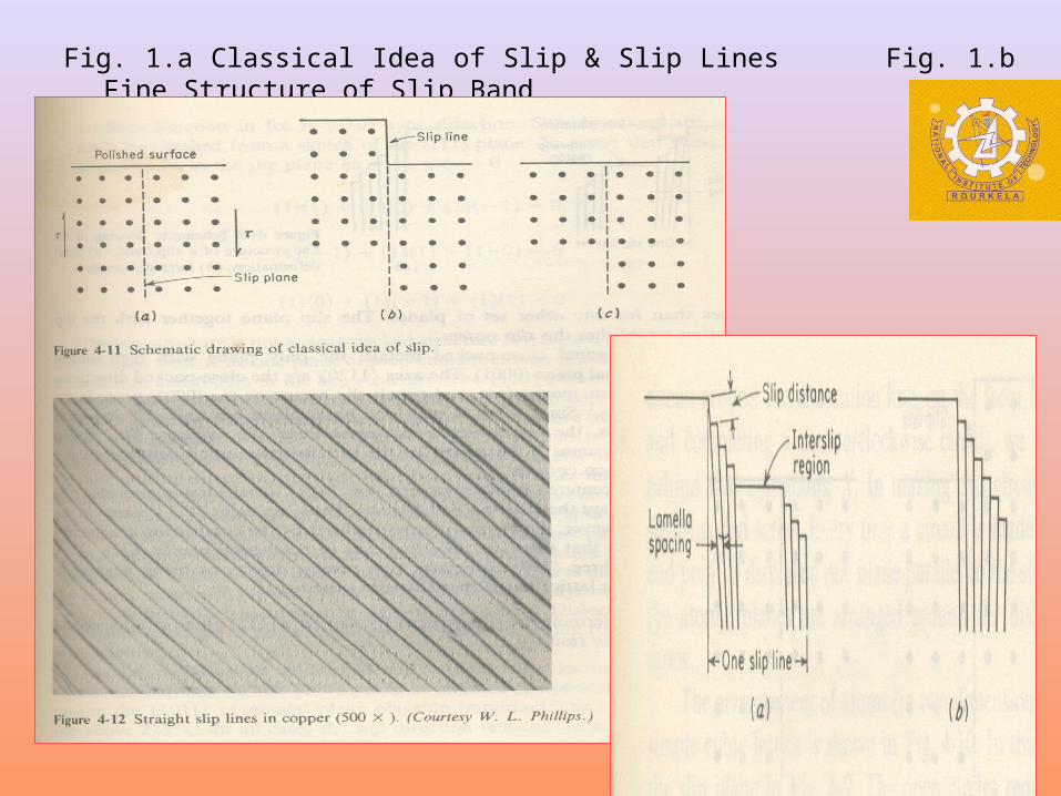
Fig. 1.a Classical Idea of Slip & Slip Lines Fig. 1.b Fine Structure of Slip Band
8
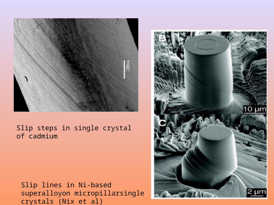
Slip steps in single crystal of cadmium
Slip lines in Ni-based superalloyon micropillarsingle crystals (Nix et al)
9
• Slip takes place along certain crystallographic planes and directions (there are only limited no. of planes and directions).
• Stress must exceed a critical level. • Slip displacement is an integral multiple of atomic distance (each atom moves an integral multiple of atomic spacing).
Due to symmetry of a crystal lattice, the crystal structure is perfectly restored, if deformation is uniform. Each atom in the slipped part move by the same integral multiple of lattice spacing.
Slip lines appears as changes in elevation. Under Electron Microscope the change in elevation of slip appears as a band. The band is actually composed of number of individual slip steps.
Effect of Shear Stress
10
Slip Plane & Direction
Slip occurs most readily in specific direction on a certain specific crystallographic planes. Generally, slip planes are plane of greatest atomic density. Slip directions are closest–packed directions within the slip planes.• Since the planes of highest atomic density are most widely spaced planes in the crystal systems, the resistance to slip is least along the set of planes. • Slip directions are closed packed direction, therefore the movement of atoms in the direction is least.• The slip plane together with the slip direction is considered as slip systems.
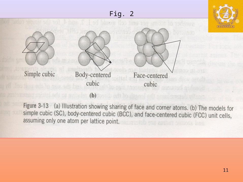
The most common crystation lattice in metallic materials are bcc, hcp and fcc. The figures show the hard ball model and stacking sequences in the above crystal systems
Slip occurs most readily in specific direction on a certain specific crystallographic planes. Generally, slip planes are plane of greatest atomic density. Slip directions are closest–packed directions within the slip planes.• Since the planes of highest atomic density are most widely spaced planes in the crystal systems, the resistance to slip is least along the set of planes. • Slip directions are closed packed direction, therefore the movement of atoms in the direction is least.• The slip plane together with the slip direction is considered as slip systems.
The most common crystation lattice in metallic materials are bcc, hcp and fcc. The figures show the hard ball model and stacking sequences in the above crystal systems
11
Fig. 2
12
hcp Crystals
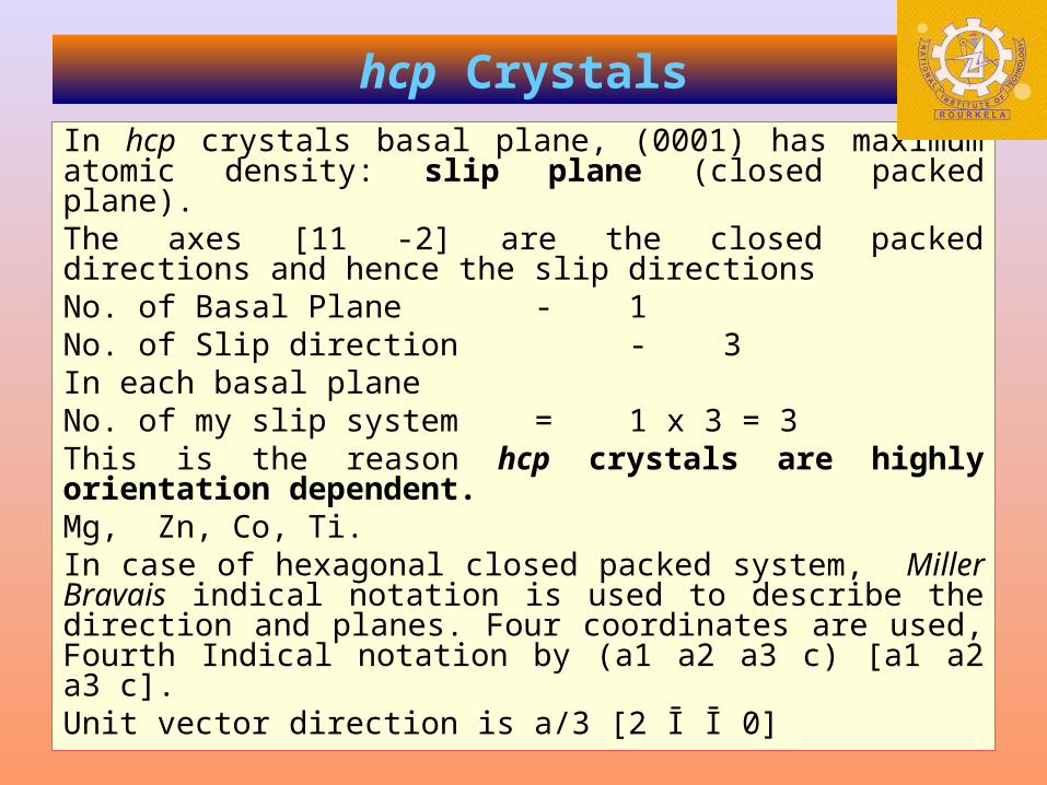
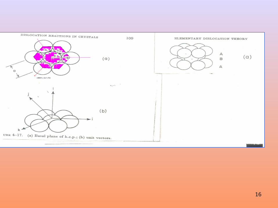
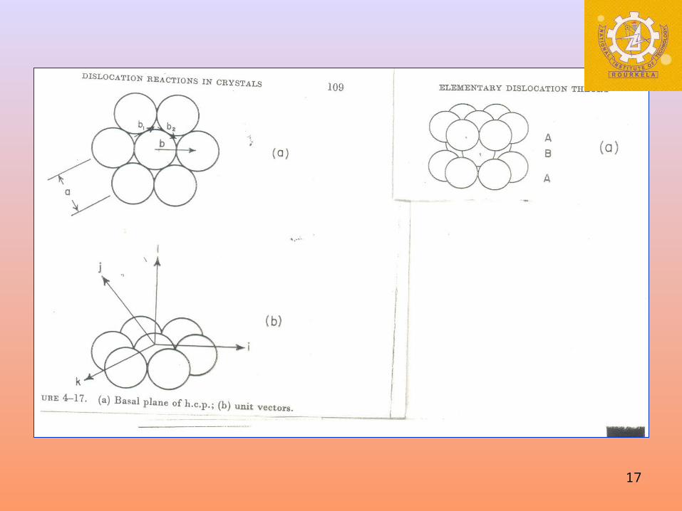
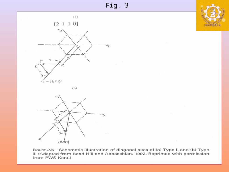
In hcp crystals basal plane, (0001) has maximum atomic density: slip plane (closed packed plane). The axes [11 -2] are the closed packed directions and hence the slip directionsNo. of Basal Plane - 1No. of Slip direction - 3In each basal planeNo. of my slip system = 1 x 3 = 3This is the reason hcp crystals are highly orientation dependent.Mg, Zn, Co, Ti.In case of hexagonal closed packed system, Miller Bravais indical notation is used to describe the direction and planes. Four coordinates are used, Fourth Indical notation by (a1 a2 a3 c) [a1 a2 a3 c].Unit vector direction is a/3 [2 Ī Ī 0]
13
Fig. 3
14
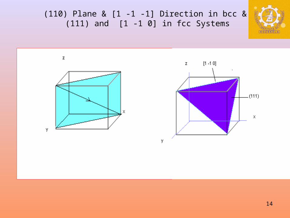
(110) Plane & [1 -1 -1] Direction in bcc & (111) and [1 -1 0] in fcc Systems
15
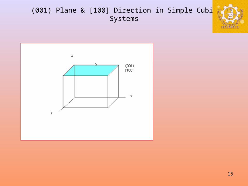
(001) Plane & [100] Direction in Simple Cubic Systems
16
17
18
Fig. 3
19
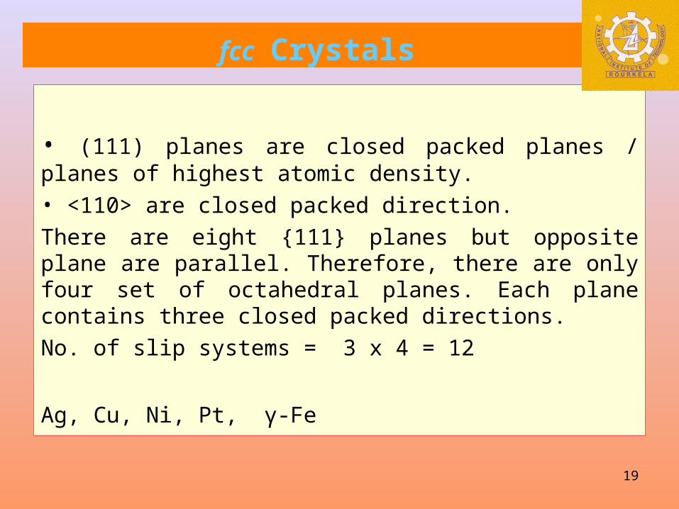
fcc Crystals
• (111) planes are closed packed planes / planes of highest atomic density. • <110> are closed packed direction.
There are eight {111} planes but opposite plane are parallel. Therefore, there are only four set of octahedral planes. Each plane contains three closed packed directions.
No. of slip systems = 3 x 4 = 12
Ag, Cu, Ni, Pt, γ-Fe
20
Slip planes/ directions in fcc
21
Slip planes/ directions in bcc
22
bcc Crystals
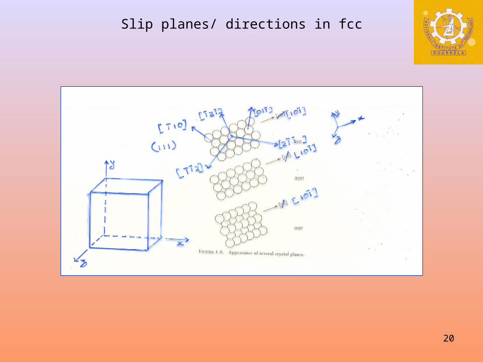
bcc is not a closed packed structure. Not even a single closed packed plane. {110} planes have higher atomic density. <111> direction are as closed as <110> in fcc and {11-20} in hcp.The slip planes are not definite • Common slip planes {110}, {112} & {123} • Directions always {111}. There are 48 slip systems. But planes are not really closed packed, therefore, the shear stress required is higher.Slip moves (cross slip) from one plane to other resulting into irregular wavy slip bands. The examples of bcc metals α – Fe, Mo, Cr, Nb.
23
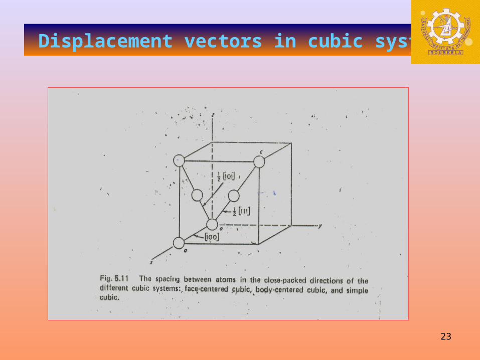
Displacement vectors in cubic system
24
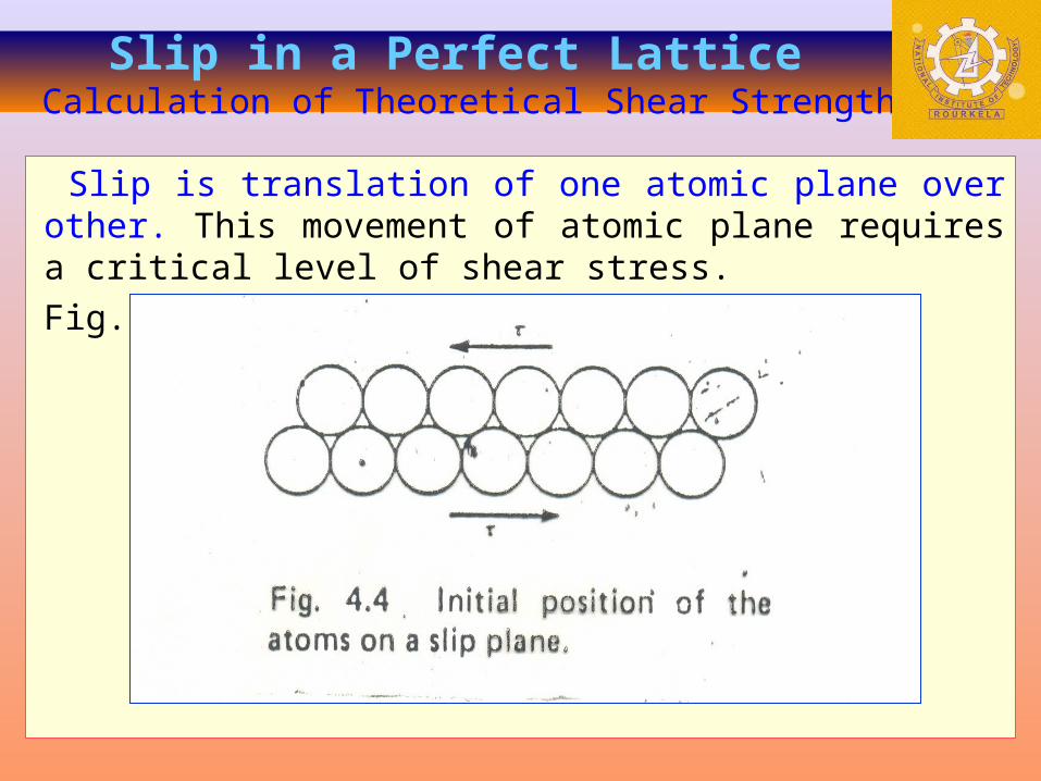
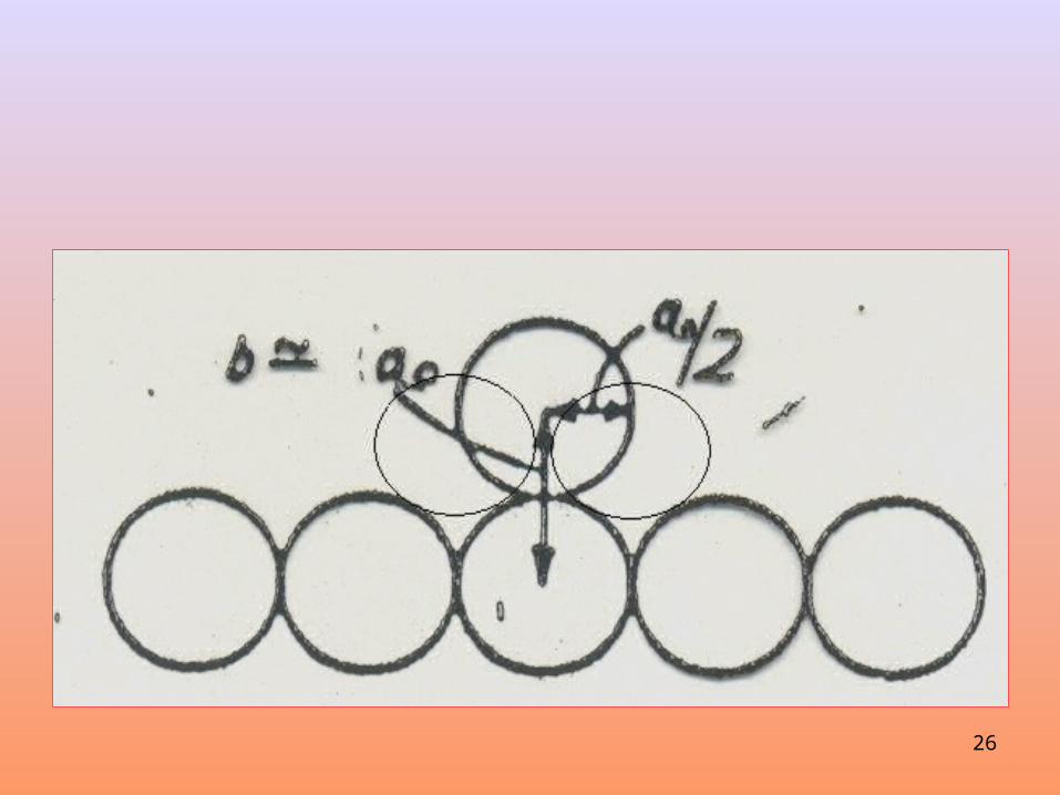
Slip in a Perfect Lattice Calculation of Theoretical Shear Strength
Slip is translation of one atomic plane over other. This movement of atomic plane requires a critical level of shear stress.
Fig.
25
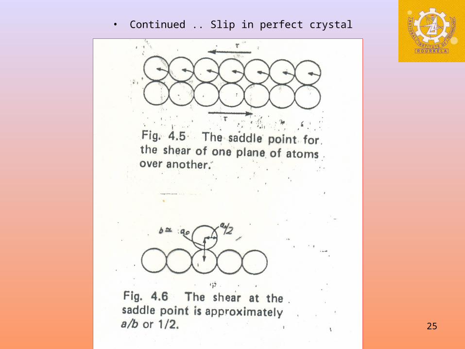
• Continued .. Slip in perfect crystal
26
27
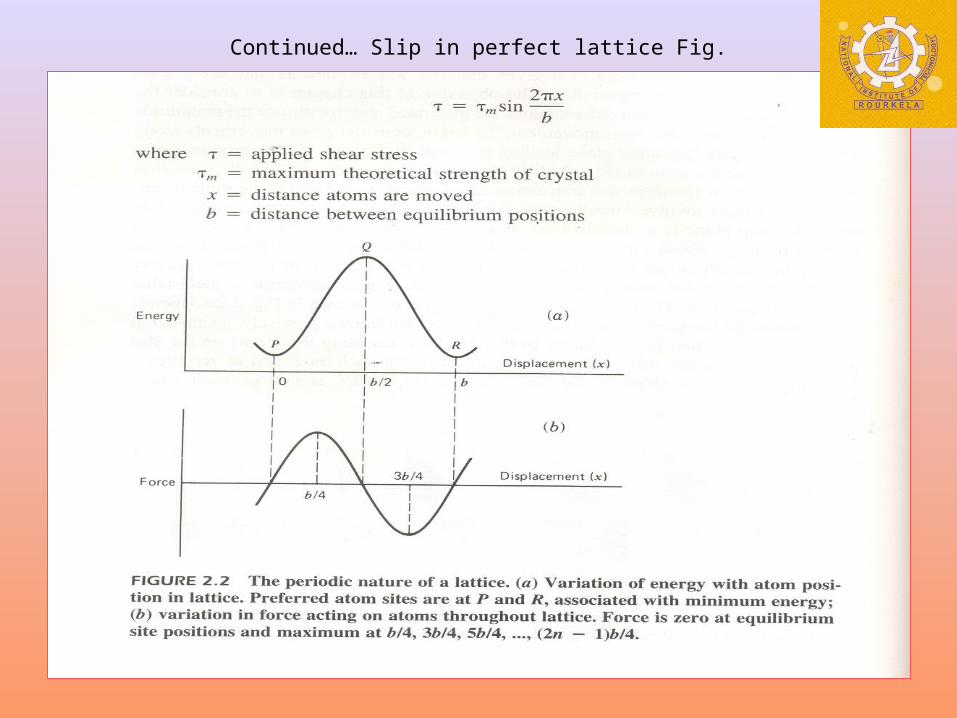
Continued… Slip in perfect lattice Fig.
28
Continued… Slip in perfect lattice Fig.
The shear stress is a periodic function of the displacement. A sinusoidal relationship can be assumed here is amplitude of sine wave. a is
interatomic spacing, b is period & x is small displacement
Now
For small displacement,
G
a
bGm
2
a
xGGr
m
29
Continued… Slip in perfect lattice Fig.
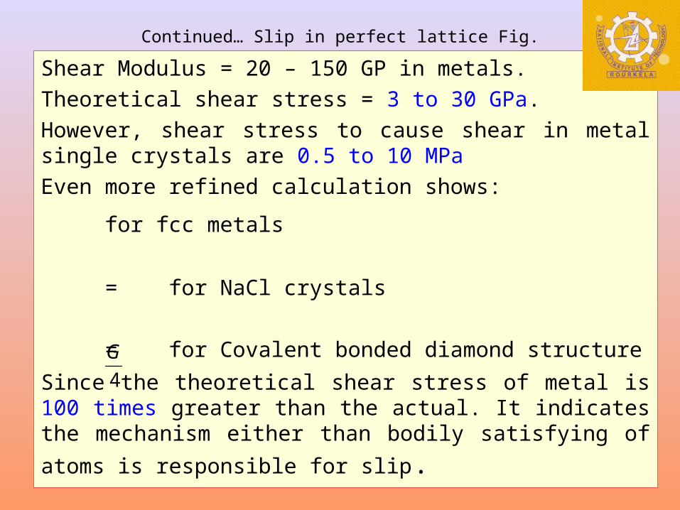
Shear Modulus = 20 – 150 GP in metals.
Theoretical shear stress = 3 to 30 GPa.
However, shear stress to cause shear in metal single crystals are 0.5 to 10 MPa
Even more refined calculation shows:
for fcc metals
= for NaCl crystals
= for Covalent bonded diamond structure
Since the theoretical shear stress of metal is 100 times greater than the actual. It indicates the mechanism either
than bodily satisfying of atoms is responsible for slip.
4
G
30
Theoretical shear strength, explanation
The concept of dislocation was first introduced to explain discrepancy between the observed and theoretical shear strength of metals If this concept is true it is necessary to show: 1) they are visible, 2) the motion of a dislocation requires a shear stress much smaller than the theoretical shear strength. 3) the movement of dislocation produces a steps at the free surface. All three are found to be true in real crystals. This indicates the validity of the concept of dislocation.
31
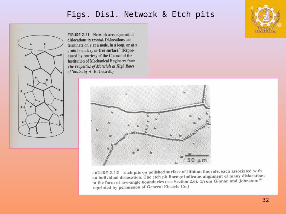
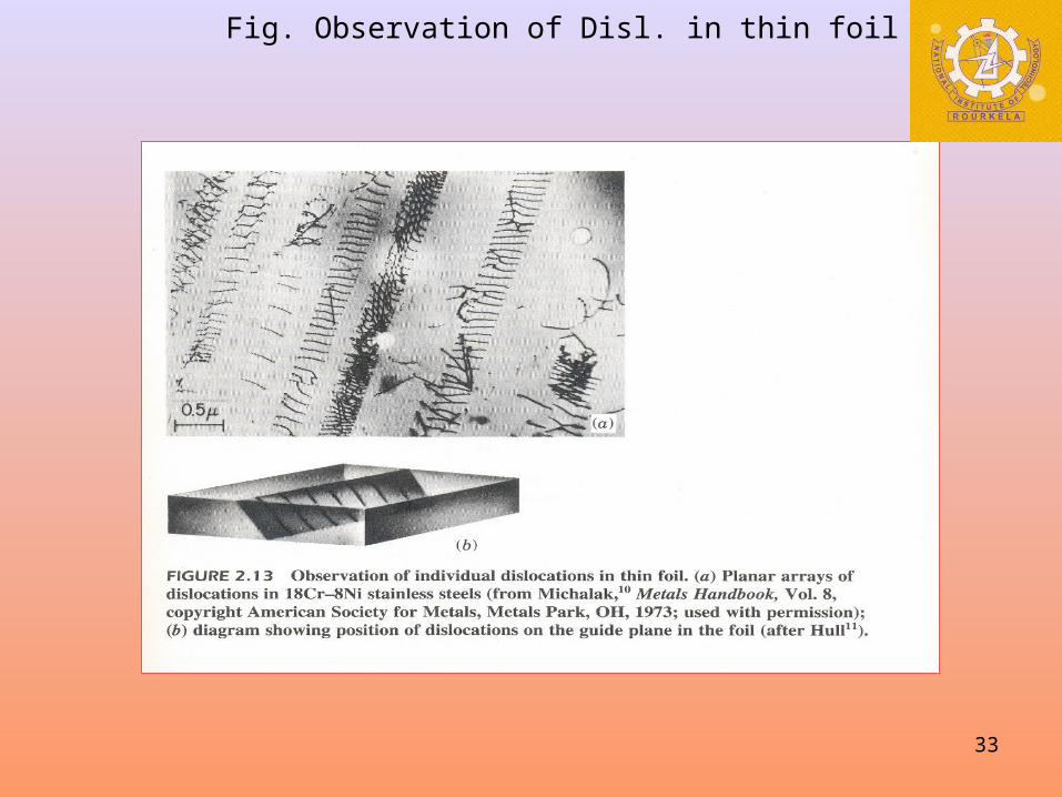
• It is possible to see these dislocations with aid of Transmission Electron Microscope.
For this purpose very thin slice of metal is taken (few thousand Ǻ thick) from a deformed crystal.
• Etch Pit Technique revels the location of intersection of dislocation line with the surface.
32
Figs. Disl. Network & Etch pits
.
33
Fig. Observation of Disl. in thin foil
34
Edge Dislocation
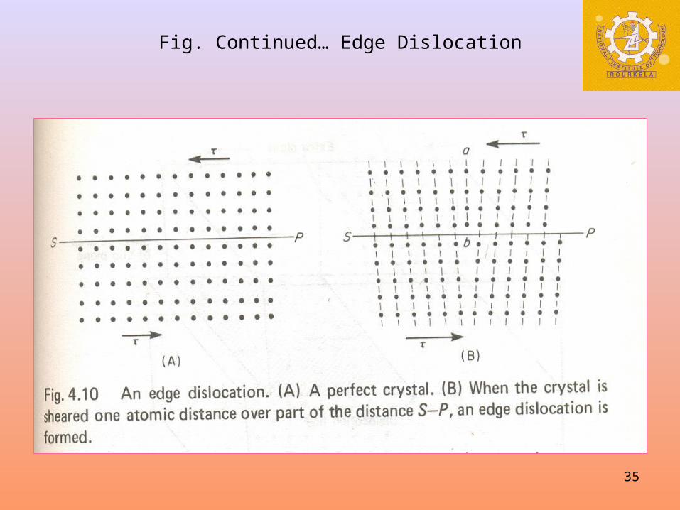
Fig – A represents a simple cubic lattice under an external shear stress. The amount of slip or displacement is assumed to be one atomic spacing. The result of this shear is shown in the Fig. – B.
• This leaves an extra half plane CD below the slip plane in the right hand side, outside the crystal.
• It will also produce an extra half plane located above the slip plane and in the centre of the crystal.
• All other planes are realigned and continuity is maintained.• Distortion decrease as moved away from the edge of the
extra plane. • The boundary of additional plane is called an edge
dislocation.
35
Fig. Continued… Edge Dislocation
36
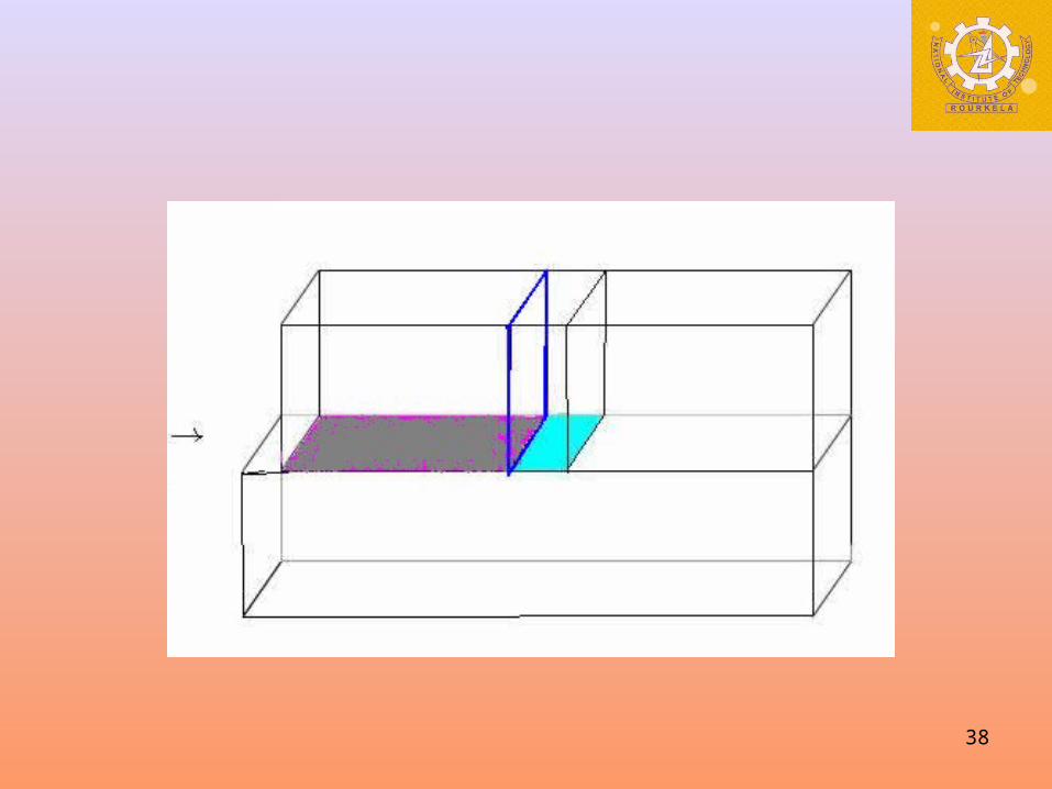
Edge Dislocation
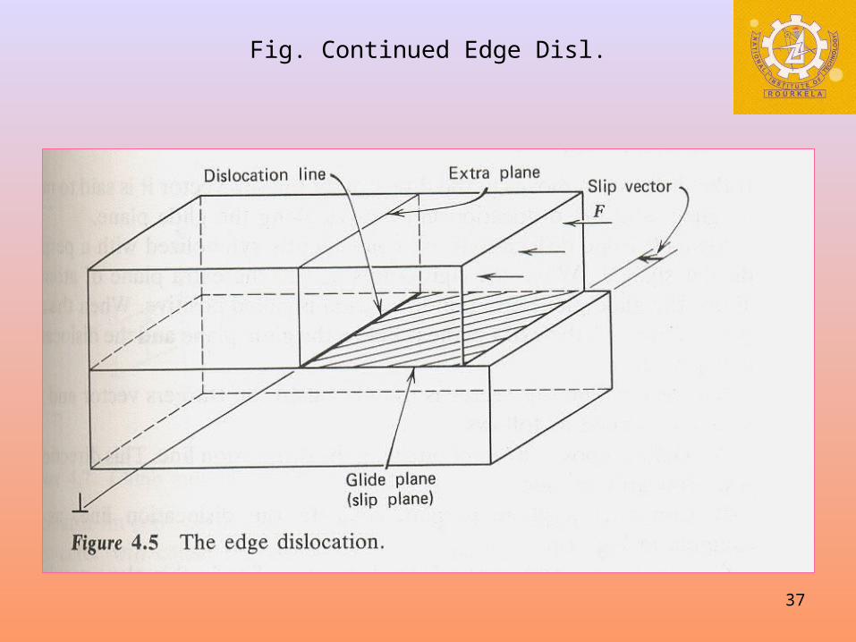
• Fig. 4.11 represents a 3 – D sketch of the edge dislocation.
• The figure clearly shows that dislocation has the dimension of a line.
• Dislocation line marks the (separates) boundary between sheared and un-sheared part of the slip plane.
This is the basic characteristics of a dislocation line. Dislocation may be defined as a line that forms a
boundary on a slip plane between slipped and un-slipped region.
Displacement vector: Burgers Vector, bֿ .
37
Fig. Continued Edge Disl.
38
39
40
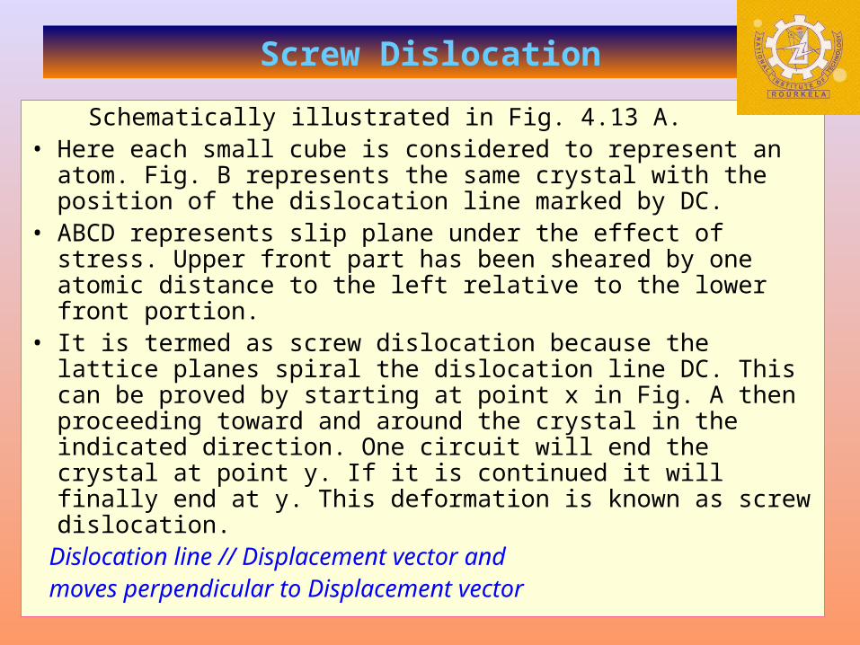
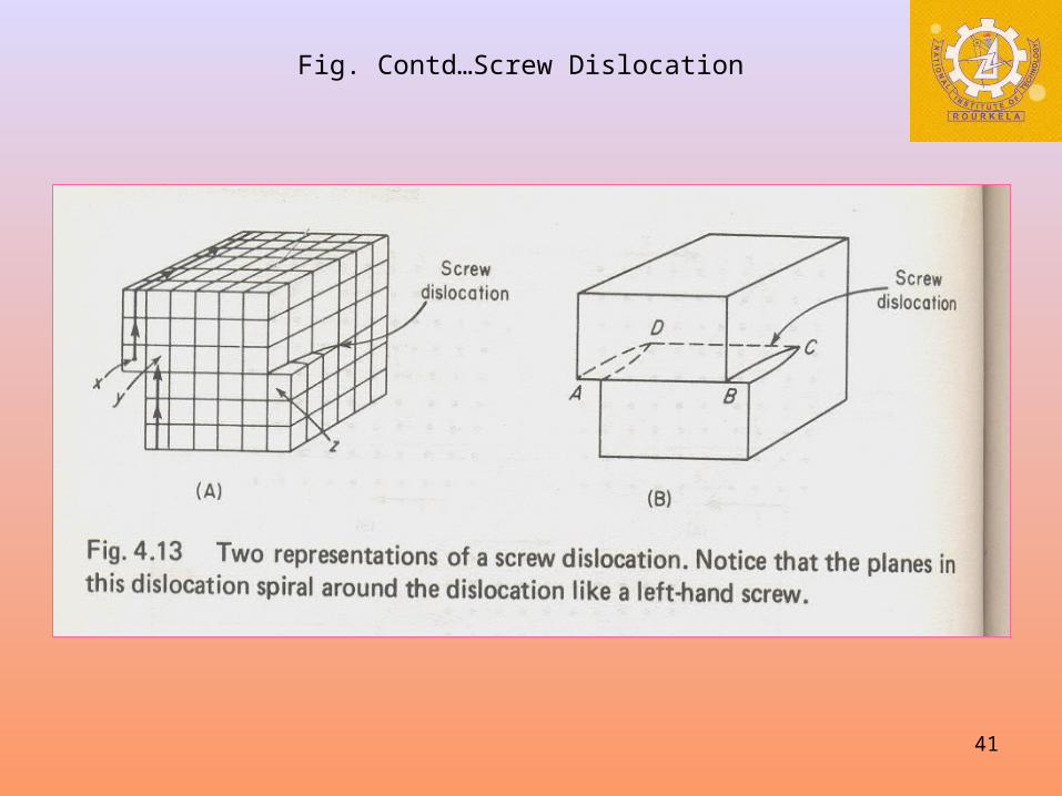
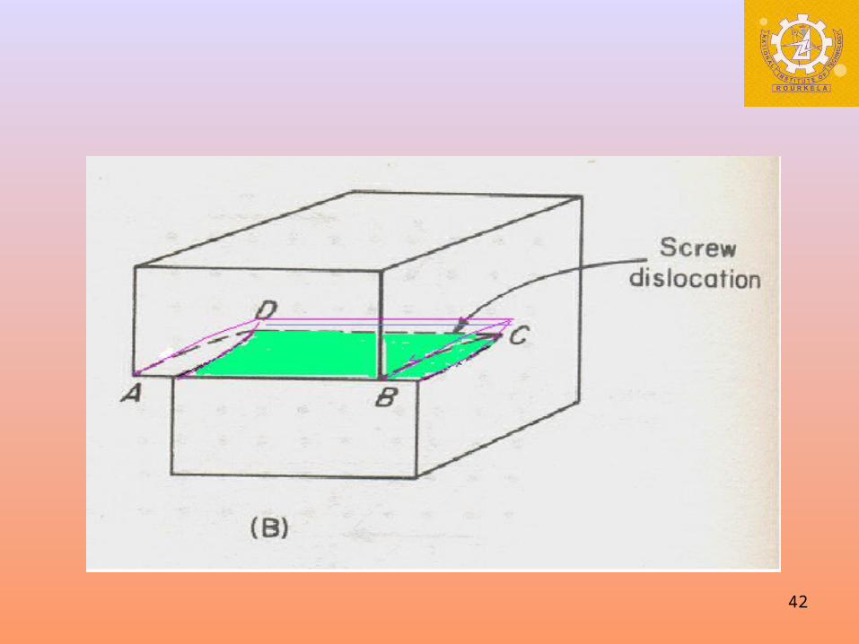
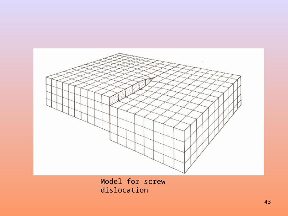
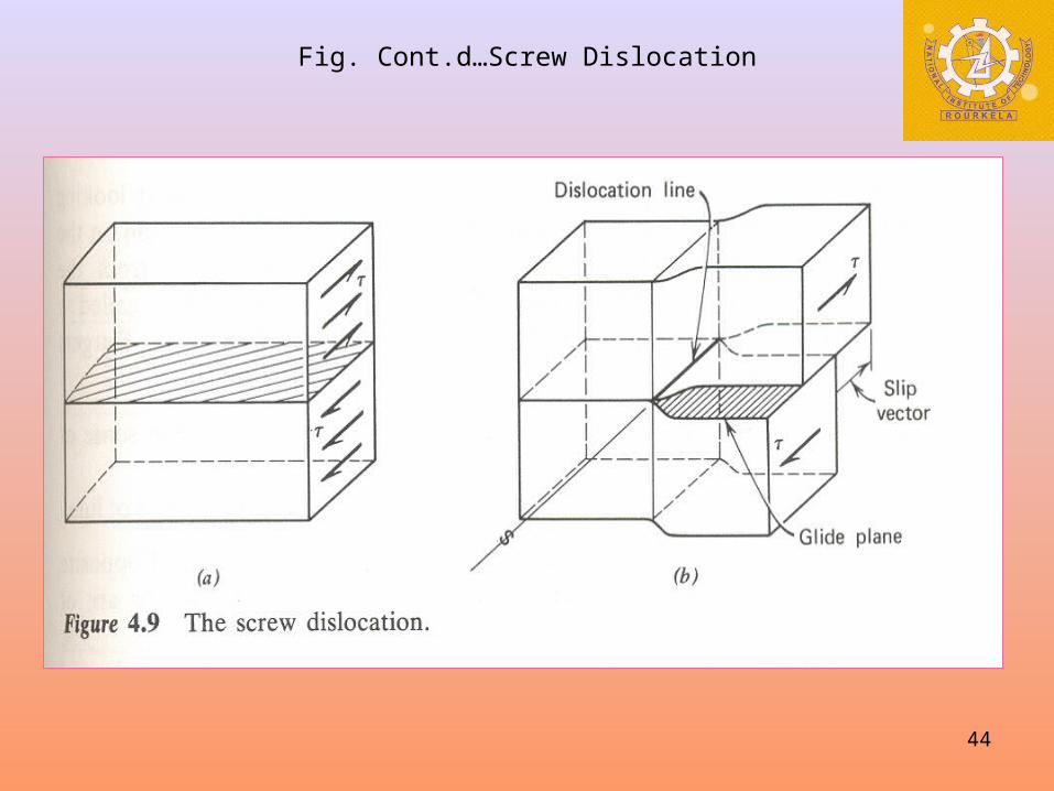
Screw Dislocation
Schematically illustrated in Fig. 4.13 A. • Here each small cube is considered to represent an atom.
Fig. B represents the same crystal with the position of the dislocation line marked by DC.
• ABCD represents slip plane under the effect of stress. Upper front part has been sheared by one atomic distance to the left relative to the lower front portion.
• It is termed as screw dislocation because the lattice planes spiral the dislocation line DC. This can be proved by starting at point x in Fig. A then proceeding toward and around the crystal in the indicated direction. One circuit will end the crystal at point y. If it is continued it will finally end at y. This deformation is known as screw dislocation.
Dislocation line // Displacement vector and moves perpendicular to Displacement vector
41
Fig. Contd…Screw Dislocation
42
43
Model for screw dislocation
44
Fig. Cont.d…Screw Dislocation
45
Edge vs Screw Dislocations
• The Fig. A, shown earlier has an incomplete plane which lies above the slip plane. These dislocations are repres-ented by and ┴. Here the “―” represents slip plane and “I” vertical line extra-half plane.
• It is also possible to introduce an incomplete plane below the slip plane these dislocations are differentiated by calling the first one as positive(┴) and second a negative (┬)edge dislocation.
• It may be noted that the difference between these dislocations is arbitrary. A single rotation of a positive edge dislocation by 180° turns it into negative edge dislocation.
46
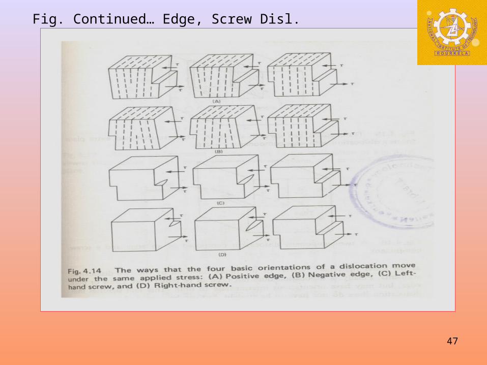
Cont… Edge vs Screw dislocations
The illustrated Screw dislocation is Left Hand Dislocation. Because the lattice planes spiral the dislocation line like a left hand screw.
In other case, lattice planes spiral the dislocation like a right hand screw (anti-clock wise movement of lattice planes results the advancement towards its operator/ right). All there dislocations are shown in the Figs. 4.14.
47
Fig. Continued… Edge, Screw Disl.
48
Cont… Edge vs Screw dislocations
• In (+) edge dislocation, line move to the left, when stress is applied on the upper half.
• In (-) edge dislocation, line moves in the right direction when stress is applied on lower half.
• Similarly anti-clock wise movement makes the advancement towards left in left handed screw.
• Anti-clock wise movement makes the advancement in the right direction in case of right hand screw dislocation.
What is common?
Continue shearing of the crystal in all cases result into formation of steps on both the surfaces.
49
Cont… Edge vs Screw dislocations
In the above cases dislocations are terminated on the surface of the crystals. However, they can also form a continues loop within it.
• In a loop two basic types of dislocations. Screw and edge dislocations.
• An irregular area can also get sheared inside the crystal.
In all the cases displacement is equal to a vector (length equal to an atomic spacing or its multiple). This is a discontinuity at which lattice shifts from un-sheared to
shear state.
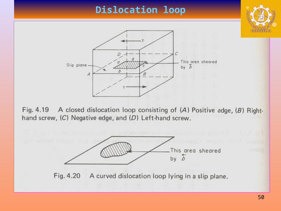
50
Dislocation loop
51
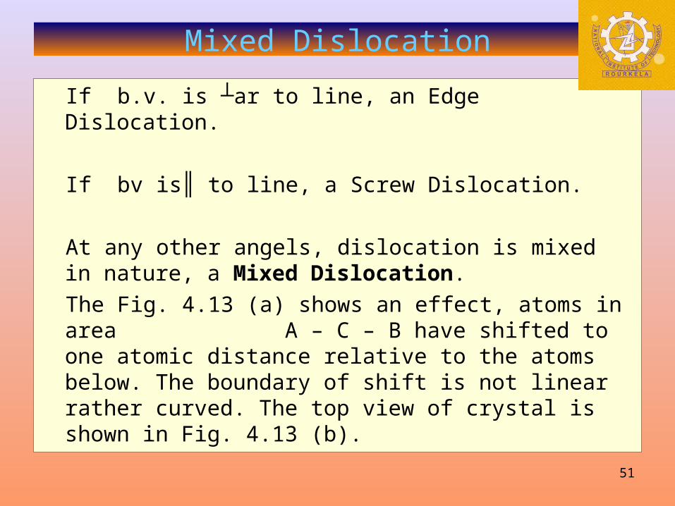
If b.v. is ┴ar to line, an Edge Dislocation.
If bv is║ to line, a Screw Dislocation.
At any other angels, dislocation is mixed in nature, a Mixed Dislocation.
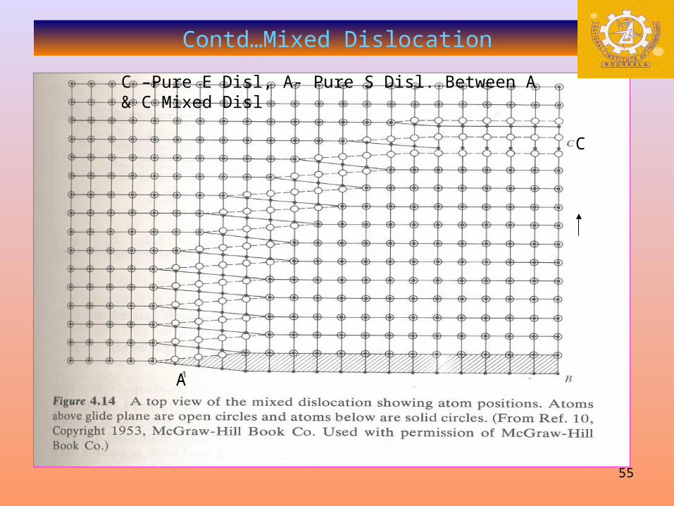
The Fig. 4.13 (a) shows an effect, atoms in area A – C – B have shifted to one atomic distance relative to the atoms below. The boundary of shift is not linear rather curved. The top view of crystal is shown in Fig. 4.13 (b).
Mixed Dislocation
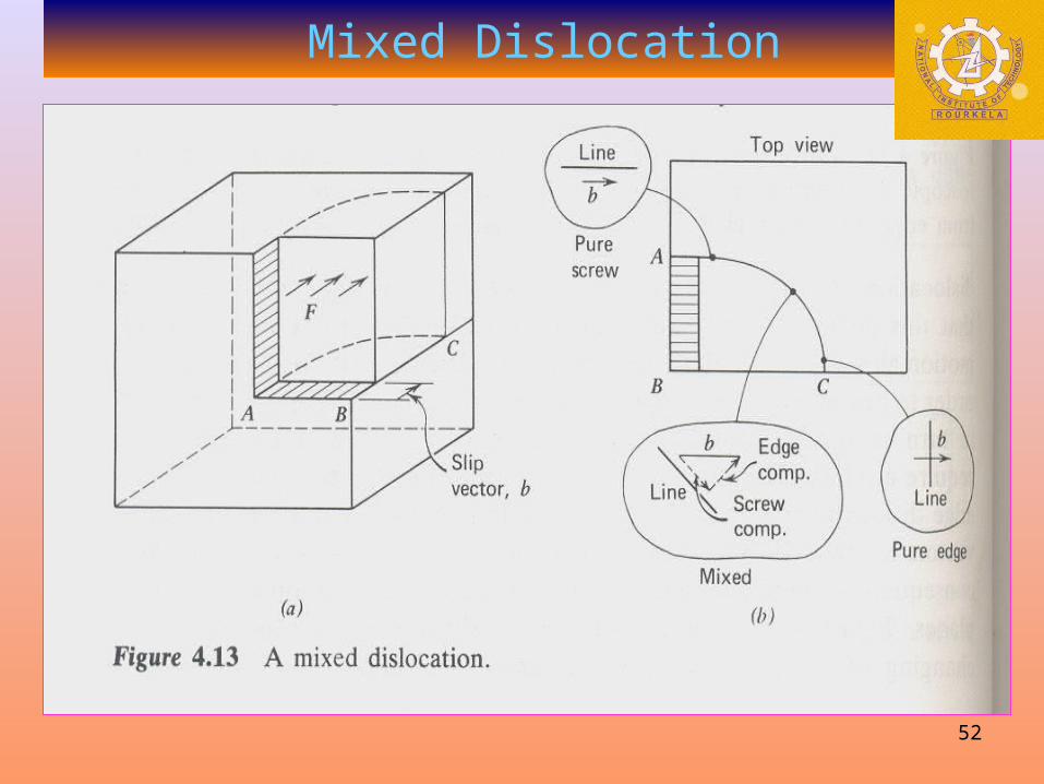
52
Mixed Dislocation
53
Cont… Mixed dislocation
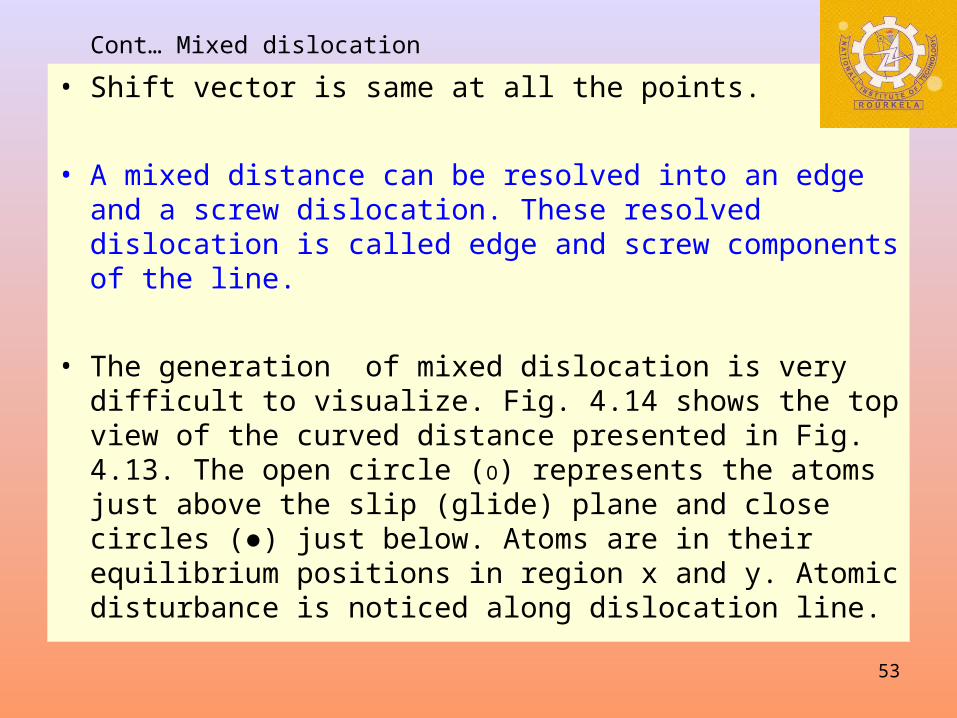
• Shift vector is same at all the points.
• A mixed distance can be resolved into an edge and a screw dislocation. These resolved dislocation is called edge and screw components of the line.
• The generation of mixed dislocation is very difficult to visualize. Fig. 4.14 shows the top view of the curved distance presented in Fig. 4.13. The open circle (O) represents the atoms just above the slip (glide) plane and close circles (●) just below. Atoms are in their equilibrium positions in region x and y. Atomic disturbance is noticed along dislocation line.

54
55
.
Contd…Mixed Dislocation
C –Pure E Disl, A- Pure S Disl. Between A & C Mixed Disl
C
A
56
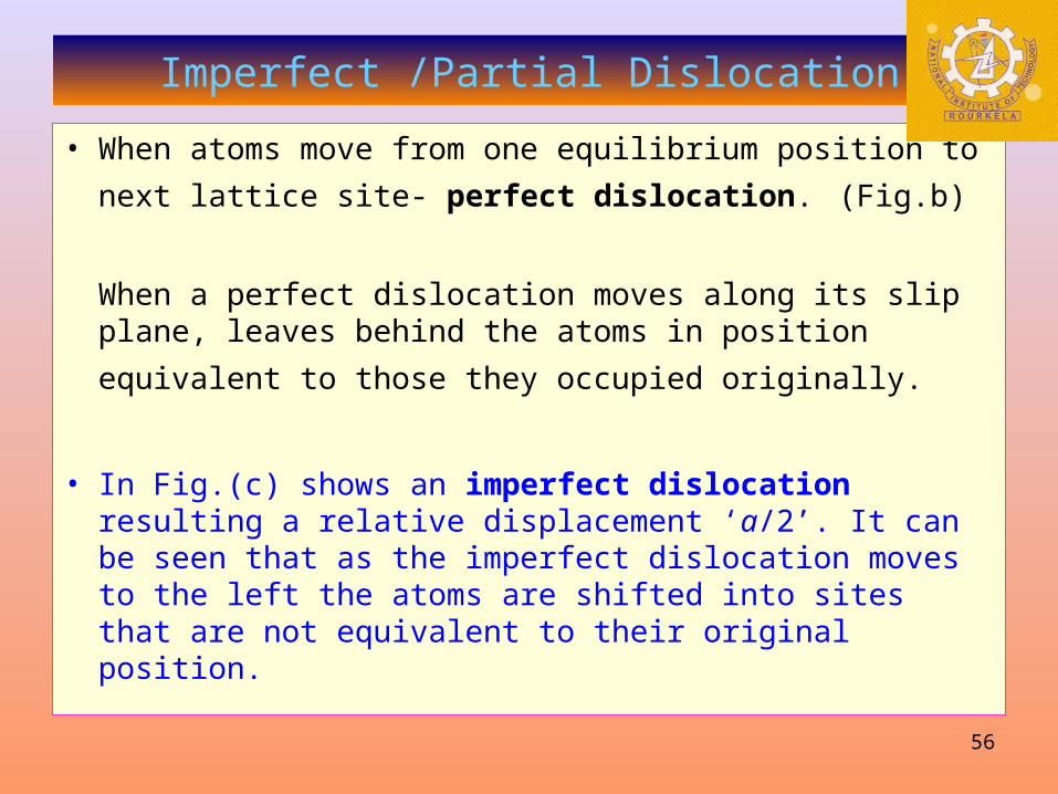
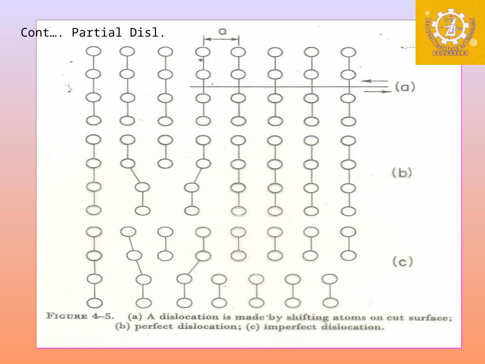
Imperfect /Partial Dislocation
• When atoms move from one equilibrium position to next
lattice site- perfect dislocation. (Fig.b)
When a perfect dislocation moves along its slip plane, leaves behind the atoms in position equivalent to those
they occupied originally.
• In Fig.(c) shows an imperfect dislocation resulting a relative displacement ‘a/2’. It can be seen that as the imperfect dislocation moves to the left the atoms are shifted into sites that are not equivalent to their original position.
57
Cont…. Partial Disl.
58
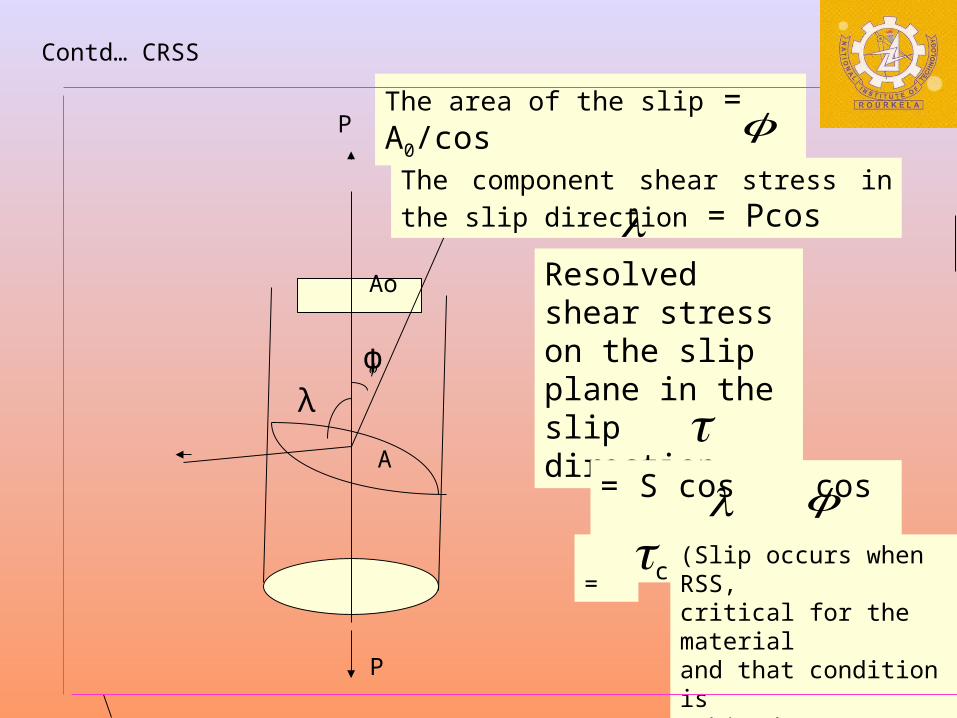
Critical Resolved Shear Stress
The extent of slip in crystal depends on the magnitude of the shearing stress produced by external loads, geom-etry of the crystal, structure and the orientation slip plane /direction with respect to the shearing stress.
Slip begins when the shearing stress (resolved) on the slip plane in the slip direction reached a critical threshold value, called critical resolved shear stress.
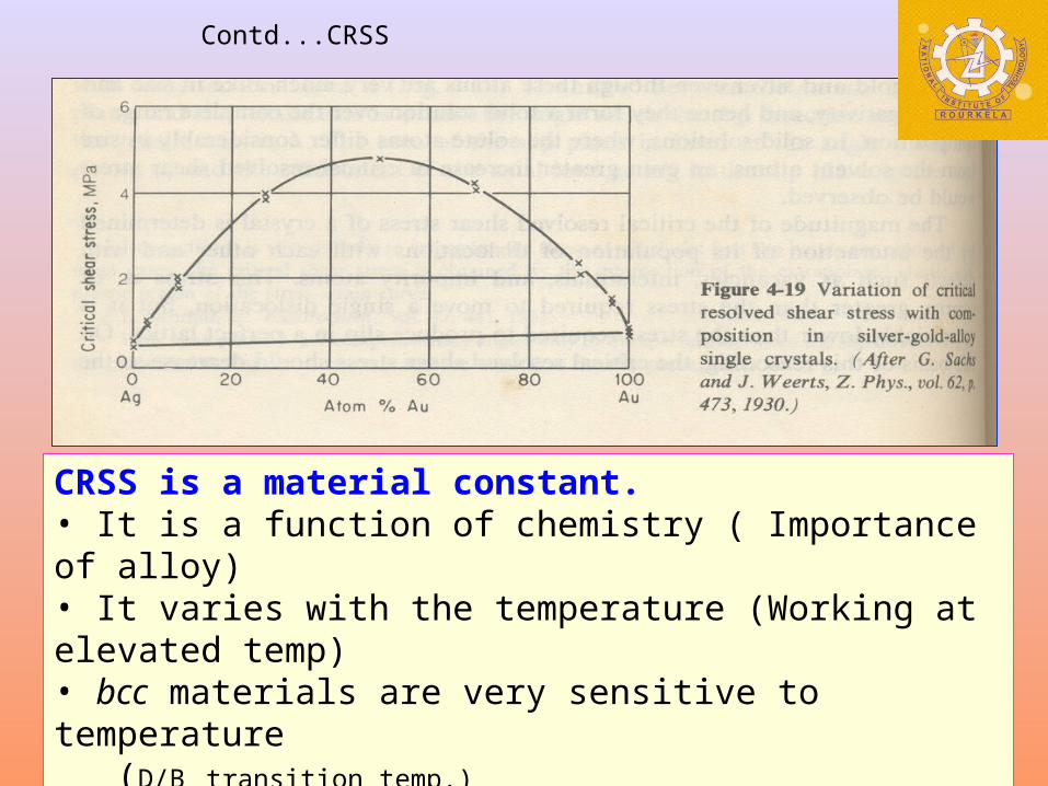
This depends on composition and temperature
(introduced by Schmid).
59
λФ
P
P
Ao
A
The area of the slip = A0/cos
The component shear stress in the slip
direction = Pcos
Resolved shear stress on the slip plane in the slip direction
= S cos cos = c
Contd… CRSS
(Slip occurs when RSS, critical for the material and that condition is achived
60
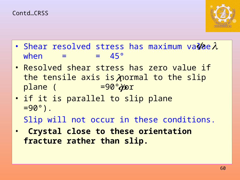
• Shear resolved stress has maximum value when = = 45°
• Resolved shear stress has zero value if the tensile axis is normal to the slip plane ( =90°)or
• if it is parallel to slip plane =90°).
Slip will not occur in these conditions.• Crystal close to these orientation fracture rather than
slip.
Contd…CRSS
61
Cont…CRSS
Contd...CRSS
CRSS is a material constant. • It is a function of chemistry ( Importance of alloy)• It varies with the temperature (Working at elevated temp)• bcc materials are very sensitive to temperature (D/B transition temp.)
• hcp crystals are very sensitive to orientation changes
62
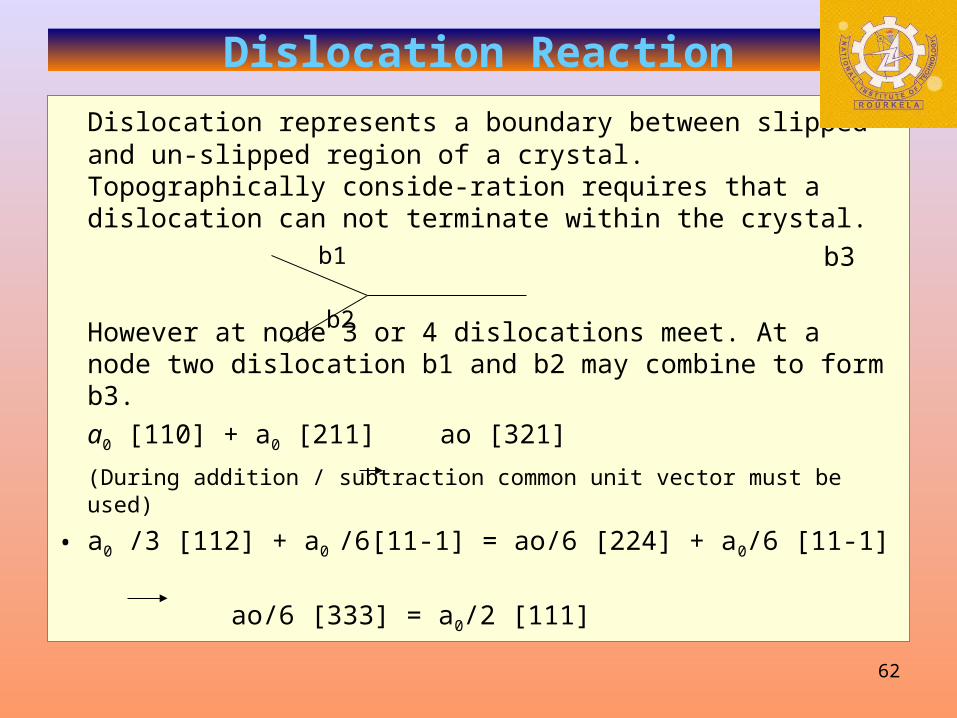
Dislocation Reaction
Dislocation represents a boundary between slipped and un-slipped region of a crystal. Topographically conside-ration requires that a dislocation can not terminate within the crystal.
b3
However at node 3 or 4 dislocations meet. At a node two dislocation b1 and b2 may combine to form b3.
a0 [110] + a0 [211] ao [321]
(During addition / subtraction common unit vector must be used)
• a0 /3 [112] + a0 /6[11-1] = ao/6 [224] + a0/6 [11-1]
ao/6 [333] = a0/2 [111]
b1
b2
63
Contd…Disl. reaction
A dislocation having b.v. equal to one lattice spacing is called distance of unit strength.
Dislocation of higher strength (2ao, 3ao…… = b.v.) They generally dissociates into the 2 or more dislocations.
Dislocation of unit strength can also dissociate. This is only possible when there is a decrease in strain
energy (proportional to the square of its b.v.)
If b = a0 [u v w]
S.E. α a02 [u2 + v2 + w2],
Strength |b| α a0 [u2 + v2 + w2]½
64
Contd… Dislocation reaction
We know that the smallest b.v. in fcc crystal is [a0 /2, a0 /2, 0] generally written as a0 /2[110] (say b)
Let us assume dissociation of this dislocation into c and d dislocations
b = c + d, a0/2 [-110] = a0/6 [-12 -1] + a0/6 [-211]
In this case vector sum of each component on the RHS is equal to LHS. (a balanced equation)
However, this is possible in case there is reduction in strain energy
b2 > c 2 + d2 feasible( reaction feasible )
65
Dislocation in fcc Lattice
• The primary slip planes in fcc lattice are (octahedral planes) [111]. The stacking sequence in this system is ABC ABC….type .See Fig.
• How can we introduce an edge dislocation?
An edge dislocation can be introduced by removing a plane of atoms (atoms upto B- stack removed, a zig –
zag row of atoms is missing , A -stack, grey circles
visible)
66
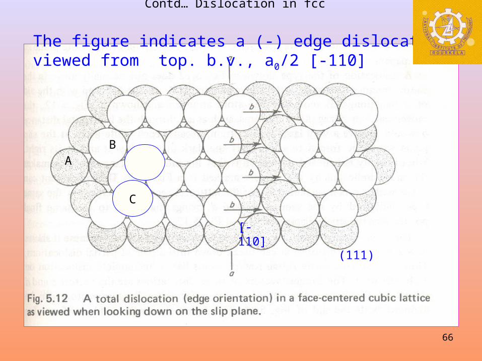
Contd… Dislocation in fcc
The figure indicates a (-) edge dislocation viewed from top. b.v., a0/2 [-110]
C
AB
[-110]
(111)
67
Cont… Dislocation in fcc
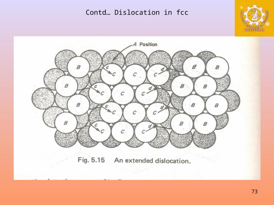
A dislocation indicated in Fig. 5.12 can not move in a simple manner.
Because in this case each white atoms have to climb over A atoms to move to next B positions.
This involves large straining of the lattice. Therefore, energetically not favorable. This displacement can also be achieved by a two step
process (this has been shown in Fig. 5.13). Atoms (B) move by vector c and then by d. This brings the atoms to same final position (B2). In other words a perfect dislocation of displacement vector b ¯ is now taking
place in two steps c ¯ and d¯. This is dissociation of b¯ into c ¯ and d ¯ resulting into introduction of two partial dislocations.
This involves less straining of crystal and therefore more energetically favorable.
68
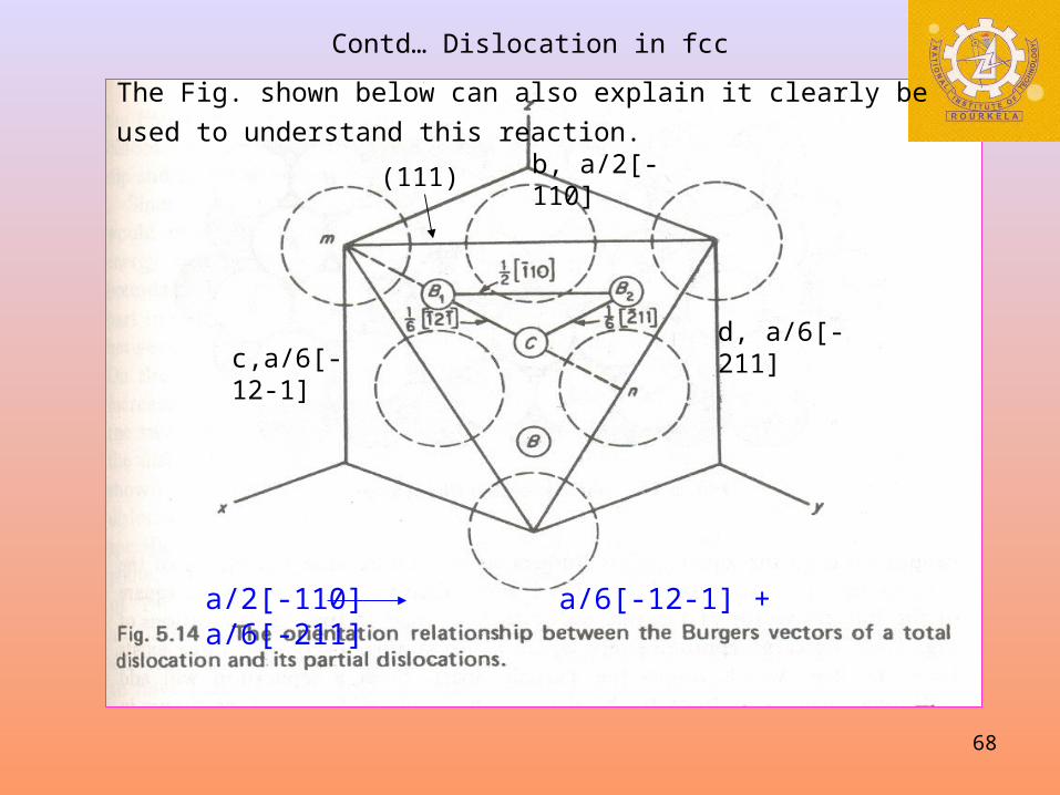
Contd… Dislocation in fcc
b, a/2[-110]
c,a/6[-12-1]d, a/6[-211]
a/2[-110] a/6[-12-1] + a/6[-211]
(111)
The Fig. shown below can also explain it clearly be used to understand
this reaction.
69
Contd… Dislocation in fcc
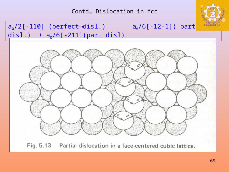
a0/2[-110] (perfect disl.) a0/6[-12-1]( partial disl.) + a0/6[-211](par. disl)
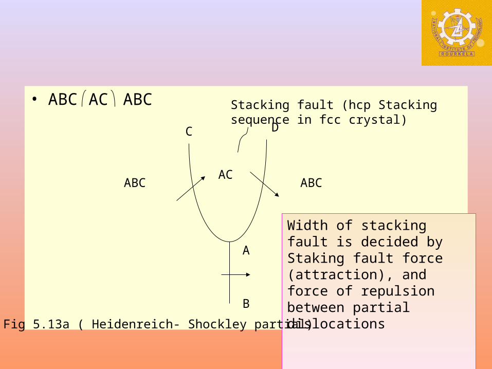
70
• ABC
ABCAC
ABC
AC ABC
A
B
C D
Stacking fault (hcp Stacking sequence in fcc crystal)
Width of stacking fault is decided by Staking fault force (attraction), and force of repulsion between partial dislocations
Fig 5.13a ( Heidenreich- Shockley partial)
71
Formation of partial dislocation can be understood with
the help of this Fig. (5.13 5.13a Reed – Hill).
Originally there is a perfect dislocation (Fig.5.12) on the
either sides of the dislocation line.
Stacking sequence is ABCABC (ABC ABC dislocation
line).
During its course of movement atoms stacked at “B”
position moves to “C” position. At this state the stacking
sequence is ABC (AC) ABC.
It is a fault in the stacking sequence, known as stacking
fault.
72
• The angle between two partial 60°. Force is repulsively
between these two partials (because they are of
opposite sign and angle θ > 45°).• The faulted region possesses a surface energy attractive
in nature (much smaller then an ordinary g.b.). • Therefore this faulted region is under two opposite
forces. • width of the fault settles at equilibrium depending
on stacking fault energy or surface energy. Lower the stacking fault energy wider the fault and few more atoms are added in the faulted region.
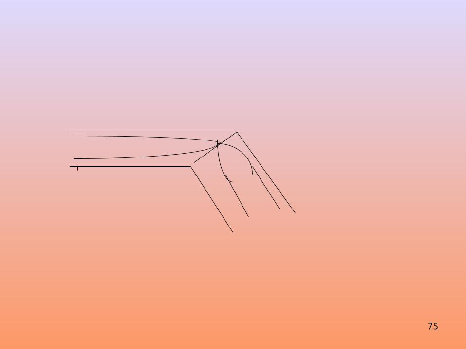
73
Contd… Dislocation in fcc
74
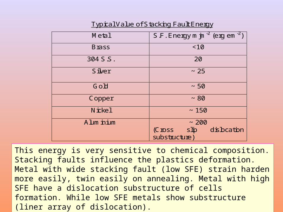
Typical Value of Stacking Fault Energy
Metal S.F. Energy mjm-2 (erg em-2)
Brass <10
304 S.S. 20
Silver ~ 25
Gold ~ 50
Copper ~ 80
Nickel ~ 150
Aluminium ~ 200 (Cross slip dislocation substructure)
This energy is very sensitive to chemical composition. Stacking faults influence the plastics deformation. Metal with wide stacking fault (low SFE) strain harden more easily, twin easily on annealing. Metal with high SFE have a dislocation substructure of cells formation. While low SFE metals show substructure (liner array of dislocation).
75
76
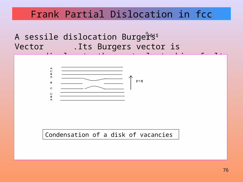
Frank Partial Dislocation in fcc
A sessile dislocation Burgers Vector .Its Burgers vector is perpendicular to the central stacking fault.
]111[3
0a
Condensation of a disk of vacancies
77
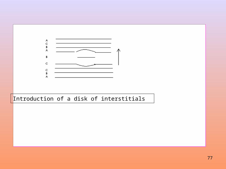
Introduction of a disk of interstitials
78
Frank pointed out that another type of partial dislocation can exist in the fcc lattice. Fig. illustrates a set of (111) planes viewed from the edge. The centre part of the middle A plane is missing. An edge dislocation if formed in this region with a Burgers vector .This is called a Frank partial dislocation. Its Burgers vector is perpendicular to the central stacking fault. Since glide must be restricted to the plane of the stacking fault and the Burgers vector is normal to this plane, the Frank partial dislocation cannot move by glide. For this reason it is called a sessile dislocation. A sessile dislocation can move only by the diffusion of atoms or vacancies to or from the fault i.e. by the process of climb.
]111[3
0a
79
Because climb is not a likely process at ordinary temperatures, sessile dislocations provide obstacles to the movement of other dislocation. Dislocations which glide freely over the slip plane, such as perfect dislocations or Shockley partials, are called glissile. A method by which a missing row of atoms can be created in the (111) plane is by the condensation of a disk of vacancies on that plane. Evidence for the collapse of disks of vacancies in aluminum has been obtained by transmission electron microscopy.
80
Lomer – Cottrell Barrier
Dislocation can glide and cross-slip (if screw in nature).Partial dislocations are created by some dislocation reactions or other mechanisms.
Shockley Partial- GlissileFrank Partial - Sessile
Sessile dislocation can also be produced by glide of dislocations on intersecting plane during duplex slip.
81
Contd… Lomer-Cottrell barrier
82
83
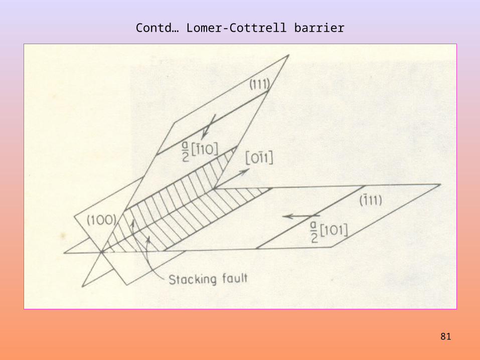
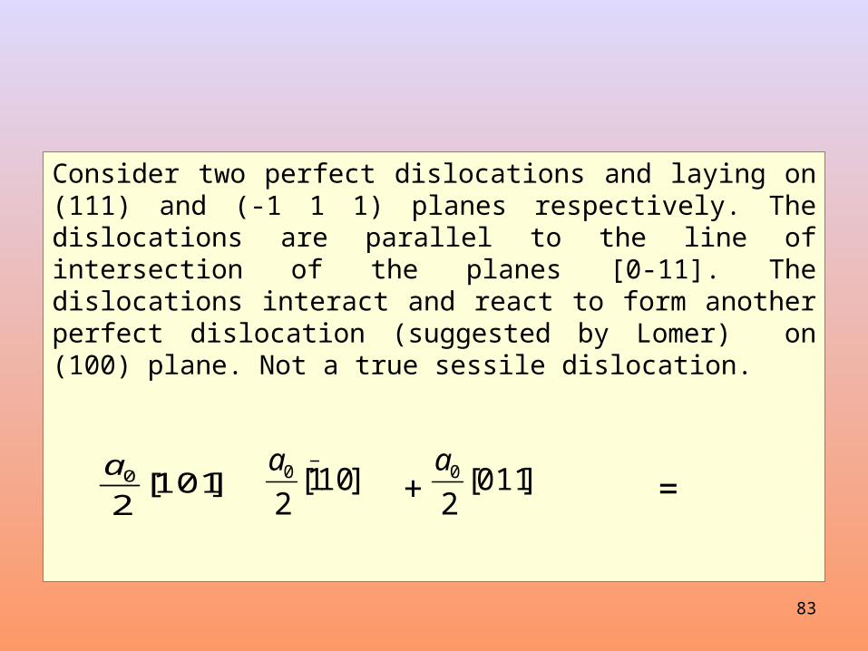
Consider two perfect dislocations and laying on (111) and (-1 1 1) planes respectively. The dislocations are parallel to the line of intersection of the planes [0-11]. The dislocations interact and react to form another perfect dislocation (suggested by Lomer) on (100) plane. Not a true sessile dislocation.
+ = ]101[2
0a ]101[2
0a ]011[2
0a
84
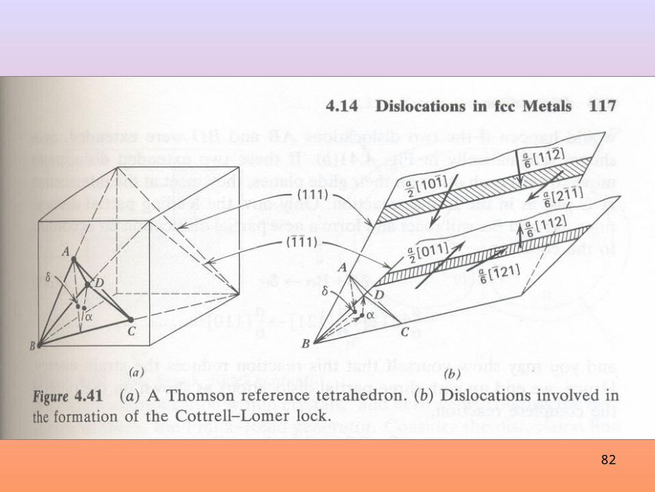
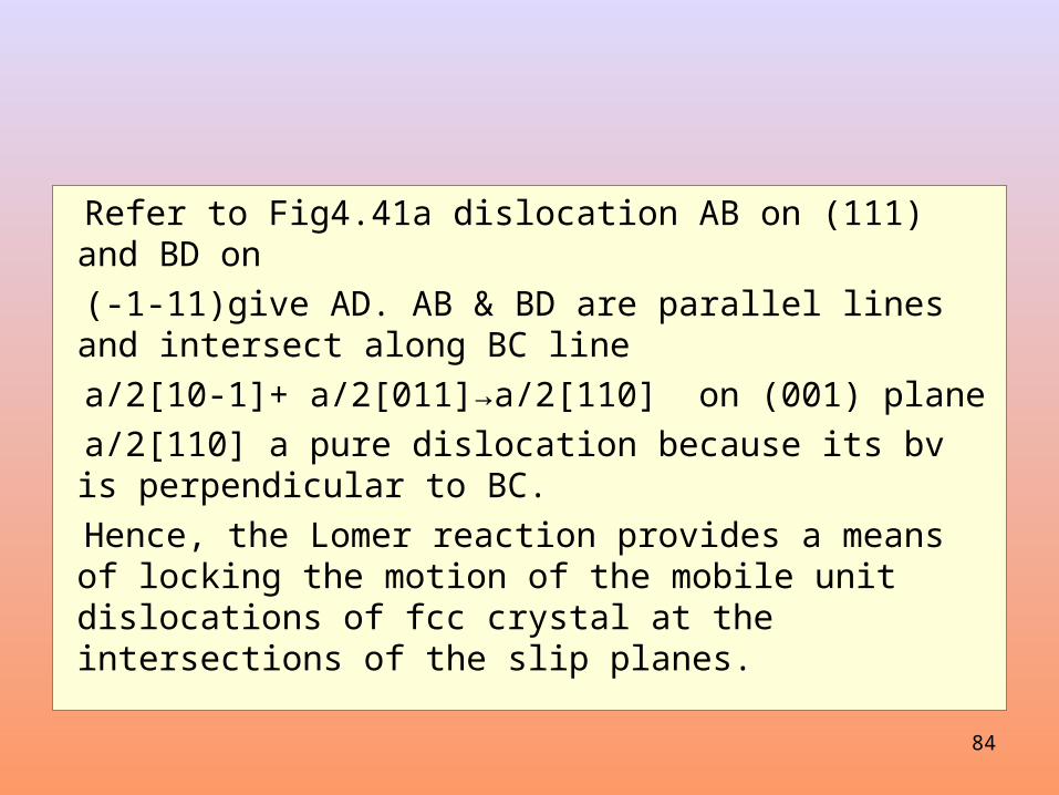
Refer to Fig4.41a dislocation AB on (111) and BD on
(-1-11)give AD. AB & BD are parallel lines and intersect along BC line
a/2[10-1]+ a/2[011]→a/2[110] on (001) plane
a/2[110] a pure dislocation because its bv is perpendicular to BC.
Hence, the Lomer reaction provides a means of locking the motion of the mobile unit dislocations of fcc crystal at the intersections of the slip planes.
85
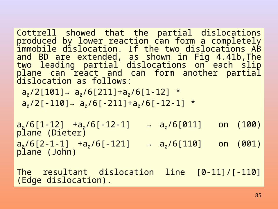
Cottrell showed that the partial dislocations produced by lower reaction can form a completely immobile dislocation. If the two dislocations AB and BD are extended, as shown in Fig 4.41b,The two leading partial dislocations on each slip plane can react and can form another partial dislocation as follows: a0/2[101]→ a0/6[211]+a0/6[1-12] * a0/2[-110]→ a0/6[-211]+a0/6[-12-1] *
a0/6[1-12] +a0/6[-12-1] → a0/6[011] on (100) plane (Dieter)a0/6[2-1-1] +a0/6[-121] → a0/6[110] on (001) plane (John)
The resultant dislocation line [0-11]/[-110](Edge dislocation).
86
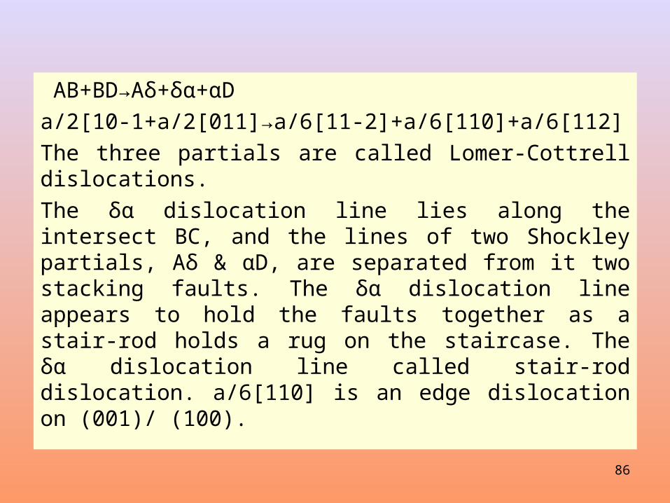
AB+BD→Aδ+δα+αD
a/2[10-1+a/2[011]→a/6[11-2]+a/6[110]+a/6[112]
The three partials are called Lomer-Cottrell dislocations.
The δα dislocation line lies along the intersect BC, and the lines of two Shockley partials, Aδ & αD, are separated from it two stacking faults. The δα dislocation line appears to hold the faults together as a stair-rod holds a rug on the staircase. The δα dislocation line called stair-rod dislocation. a/6[110] is an edge dislocation on (001)/ (100).
87
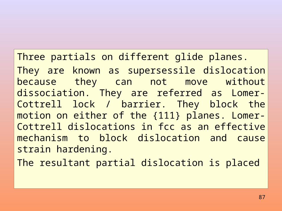
Three partials on different glide planes.
They are known as supersessile dislocation because they can not move without dissociation. They are referred as Lomer-Cottrell lock / barrier. They block the motion on either of the {111} planes. Lomer-Cottrell dislocations in fcc as an effective mechanism to block dislocation and cause strain hardening.
The resultant partial dislocation is placed
88
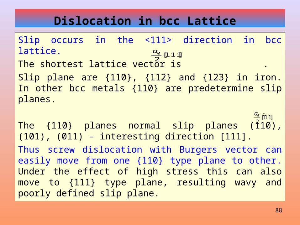
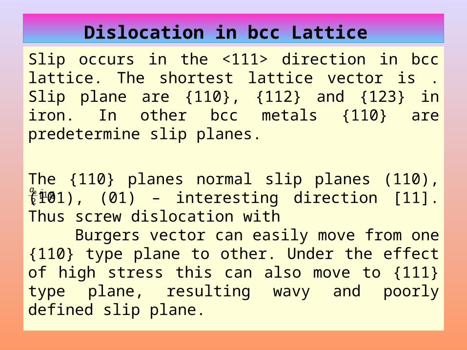
Dislocation in bcc Lattice Slip occurs in the <111> direction in bcc lattice.
The shortest lattice vector is .
Slip plane are {110}, {112} and {123} in iron. In other bcc metals {110} are predetermine slip planes.
The {110} planes normal slip planes (110), (101), (011) – interesting direction [111].
Thus screw dislocation with Burgers vector can easily move from one {110} type plane to other. Under the effect of high stress this can also move to {111} type plane, resulting wavy and poorly defined slip plane.
]111[2
0a
]111[2
0a
89
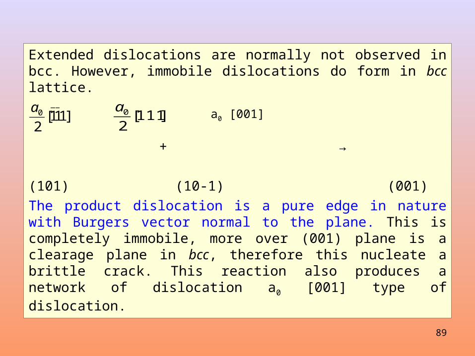
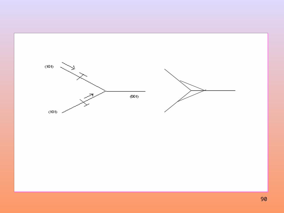
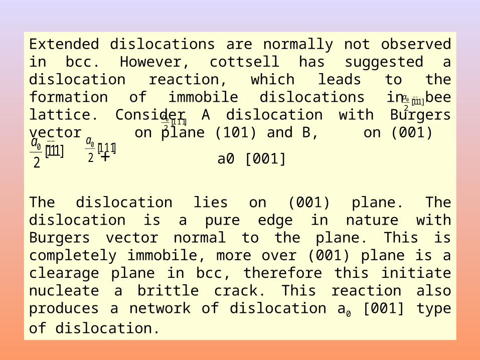
Extended dislocations are normally not observed in bcc. However, immobile dislocations do form in bcc lattice.
+ →
(101) (10-1) (001)
The product dislocation is a pure edge in nature with Burgers vector normal to the plane. This is completely immobile, more over (001) plane is a clearage plane in bcc, therefore this nucleate a brittle crack. This reaction also produces a network of dislocation a0 [001] type of dislocation.
]111[2
0a ]111[2
0a a0 [001]
90
91
Dislocation in bcc Lattice Slip occurs in the <111> direction in bcc lattice. The shortest lattice vector is . Slip plane are {110}, {112} and {123} in iron. In other bcc metals {110} are predetermine slip planes.
The {110} planes normal slip planes (110), (101), (01) – interesting direction [11]. Thus screw dislocation with Burgers vector can easily move from one {110} type plane to other. Under the effect of high stress this can also move to {111} type plane, resulting wavy and poorly defined slip plane.
]111[2
0a
92
Extended dislocations are normally not observed in bcc. However, cottsell has suggested a dislocation reaction, which leads to the formation of immobile dislocations in bee lattice. Consider A dislocation with Burgers vector on plane (101) and B, on (001)
+ a0 [001]
The dislocation lies on (001) plane. The dislocation is a pure edge in nature with Burgers vector normal to the plane. This is completely immobile, more over (001) plane is a clearage plane in bcc, therefore this initiate nucleate a brittle crack. This reaction also produces a network of dislocation a0 [001] type of dislocation.
]111[2
0a
]111[2
0a
]111[2
0a ]111[2
0a
93
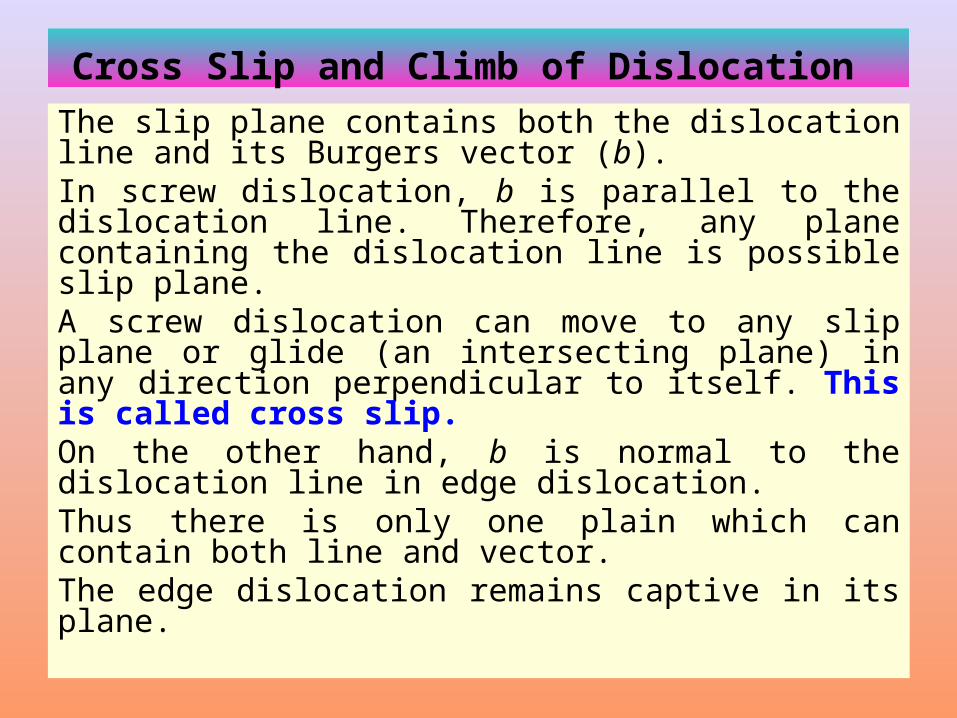
Cross Slip and Climb of Dislocation The slip plane contains both the dislocation line and its Burgers vector (b). In screw dislocation, b is parallel to the dislocation line. Therefore, any plane containing the dislocation line is possible slip plane. A screw dislocation can move to any slip plane or glide (an intersecting plane) in any direction perpendicular to itself. This is called cross slip. On the other hand, b is normal to the dislocation line in edge dislocation. Thus there is only one plain which can contain both line and vector. The edge dislocation remains captive in its plane.
94
Cross Slip and Climb of Dislocation
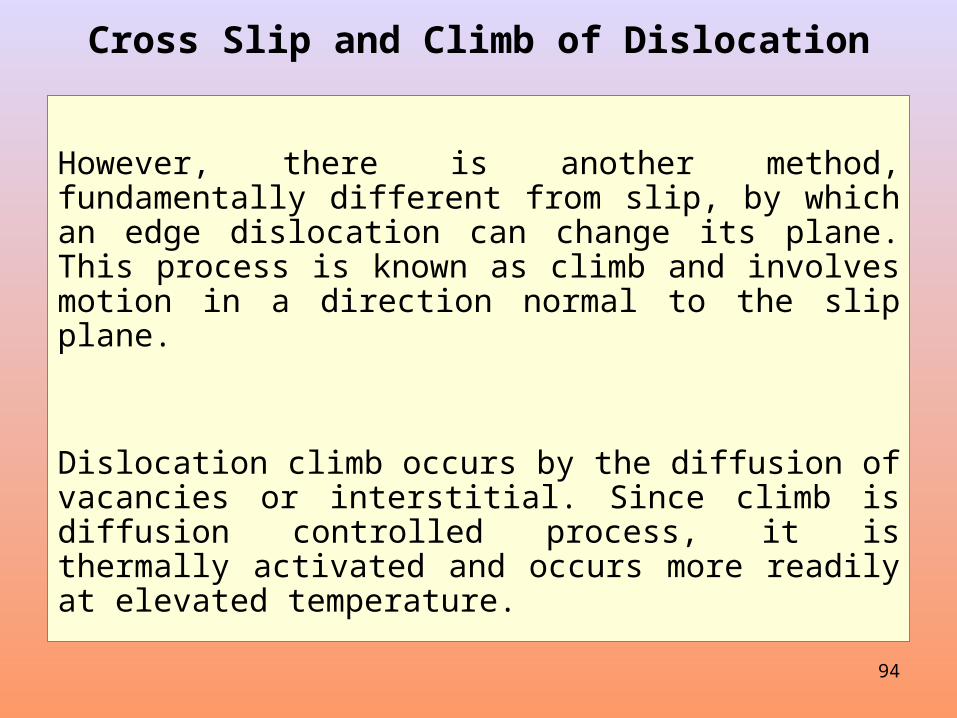
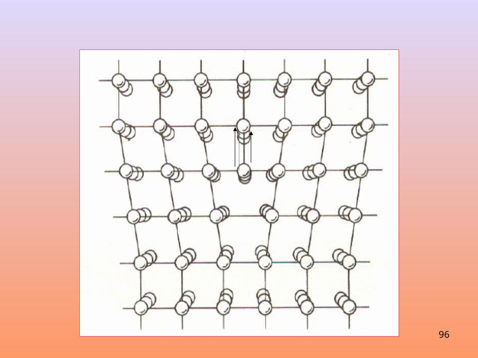
However, there is another method, fundamentally different from slip, by which an edge dislocation can change its plane. This process is known as climb and involves motion in a direction normal to the slip plane.
Dislocation climb occurs by the diffusion of vacancies or interstitial. Since climb is diffusion controlled process, it is thermally activated and occurs more readily at elevated temperature.
95
Cross Slip and Climb of Dislocation
96
97
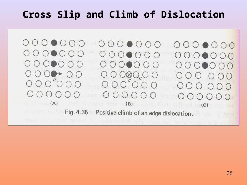
In the diagram, a vacant site has moved to position ‘a’ of the crystal. The edge dislocations lose one atom. Atom c
(crossed circle) represents the next atom of the edge (lying just below the plane of the paper). If atom c and all other atoms forming edge of dislocation move off through interaction with vacancies, the edge dislocation will climb one atom distance in a direction normal to the slip plane. The climb illustrated in this Fig. shows movement of dislocation one atomic spacing above the slip plane, designated positive climb. This results in shrinking of the size of extra plane.
98
99
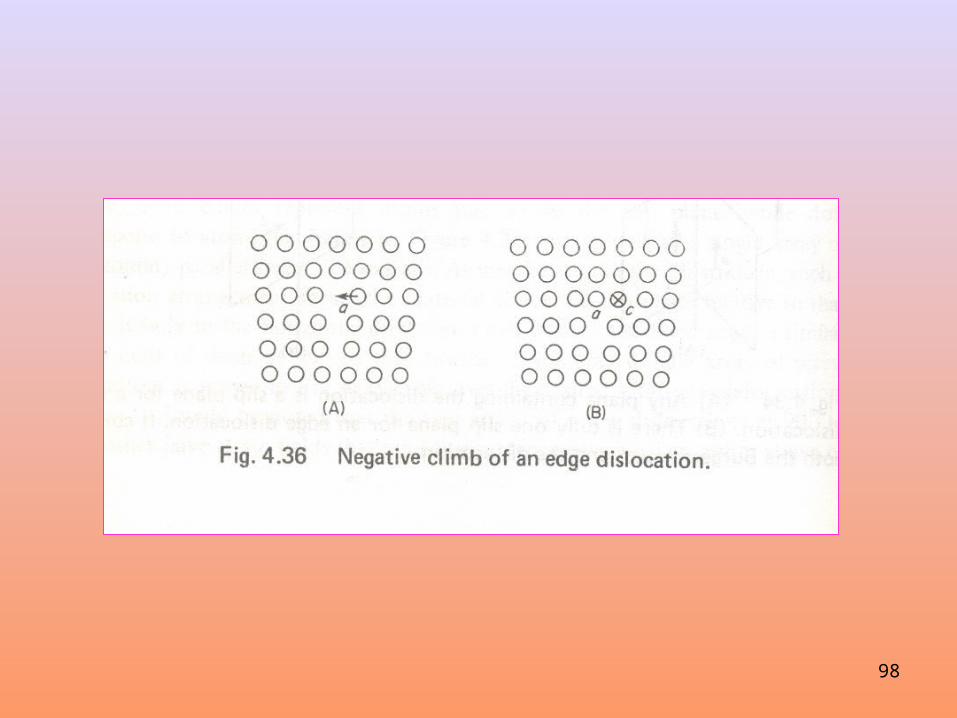
A mechanism for negative climb is illustrated in Fig. 4.36A and B. In this case atom a moves to the left and occupying a position just the below of the extra plane. This result a vacancy formation. This vacancy then moves off into the crystal. The atom just behind the plane of paper is representing by point C. This shift of the slip plane is called negation climb.Notice that this is again an atom by atom procedure. There is not a cooperative movement of the entire row of atoms (in case of slip a cooperative movement of the entire atoms takes place).
100
In case of positive climb, the extra plane grows smaller and slip plane moves in upward direction. This results shrinking of the crystal parallel to the slip plane and perpendicular to the extra plane.
Positive climb is associated with the compressive strain and is promoted by a compressive stress component perpendicular to the extra plane. In the same way, a tensile stress component perpendicular to the extra plane may cause growth of the extra plane and as a result negative climb of the dislocation.
It may be noted that slip in crystal is a result of shear stress, where as climb is associated with the normal stresses (tensile or compressive).
101
If the concentration of vacancy is very low and their rate of jump, from one equilibrium site to another equilibrium site, is low. Climb is not a likely process at low/ room temperature.
However, at high temperature the number of vacancies increase by many power of ten, as well as rate of jump (diffusivity) is very high.
Therefore, climb is promoted at high temperature. It may also be noted slip on the other hand is only slightly influenced by temperature.
102
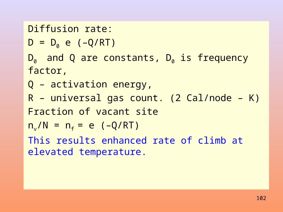
Diffusion rate:
D = D0 e (–Q/RT)
D0 and Q are constants, D0 is frequency factor,
Q – activation energy,
R – universal gas count. (2 Cal/node – K)
Fraction of vacant site
nv/N = nf = e (–Q/RT)
This results enhanced rate of climb at elevated temperature.