defects of cigs solar cells - researcher - ibm
TRANSCRIPT

www.advenergymat.de

© 2011 WILEY-VCH Verlag GmbH & Co. KGaA, Weinheim
FULL P
APER
845wileyonlinelibrary.com
www.MaterialsViews.comwww.advenergymat.de
Adv. Energy Mater. 2011, 1, 845–853
optical absorption as a direct band-gap semiconductor [ 3 ] , 2) electrically benign grain boundaries due in part to large atomic relaxation, [ 4 ] and 3) reduced usage of the toxic element cadmium (i.e., com-pared with CdTe solar cells), [ 5 ] is an attrac-tive material candidate for the absorber layer in PV devices. Record laboratory-scale power conversion effi ciency is above 20% for CIGS PV devices, [ 6 ] the highest among all thin-fi lm type solar cells. Although CIGS fi lms in record devices are deposited by a vacuum-based co-evaporation process, non-vacuum-based deposition techniques, such as chalcogenide-hydrazine complex precursors, [ 7–9 ] oxide/chalcogenide nano-particle precursors, [ 10–14 ] and electrodeposi-tion, [ 15 ] are attracting increasing attention due to their potential to achieve lower cost and larger volume manufacturing, with advantages including 1) lower equipment capital costs, 2) higher throughput, 3) more convenient scale-up potential for large area processing, and 4) higher materials utiliza-tion rate, compared with vacuum based deposition techniques. [ 16 , 17 ]
Despite the great progress made on optimizing the deposition process and PV
performance of CIGS devices, the development of this material and associated PV technology has been accomplished mainly on an empirical basis, where improvements have been found by trial and error. Knowledge about defects in CIGS, especially their correlation with process conditions and material proper-ties as well as their infl uences on device performance, is still incomplete. [ 18 , 19 ] Controversies have surrounded the interpreta-tion of defect levels observed in admittance spectroscopy and phenomena such as the partial saturation of the device forward current (rollover) and crossing of dark and illuminated current density-voltage ( J – V ) curves (crossover) observed in current-voltage ( I – V ) characteristics of CIGS solar cells, whose origins have been attributed to Fermi-level pining at the interface, [ 20 , 21 ] bulk defects in CIGS, [ 22 , 23 ] non-Ohmic contact between CIGS and Mo, [ 24–26 ] deep acceptor defects in the CdS buffer layer, [ 27–30 ] and the existence of a defective chalcopyrite layer, sometimes referred to as an order defect compound (ODC) phase, close to the heterojunction. [ 31–38 ]
Dr. D. B. Mitzi , Dr. Q. Cao , Dr. O. Gunawan , Dr. M. Copel , Dr. K. B. Reuter , Dr. S. Jay Chey IBM T.J. Watson Research CenterYorktown Heights, NY 10598, USAE-mail: [email protected] Dr. V. R. Deline IBM Almaden Resesarch CenterSan Jose, CA 95120, USA
DOI: 10.1002/aenm.201100344
Qing Cao , Oki Gunawan , Matthew Copel , Kathleen B. Reuter , S. Jay Chey , Vaughn R. Deline , and David B. Mitzi*
Defects in Cu(In,Ga)Se 2 Chalcopyrite Semiconductors: A Comparative Study of Material Properties, Defect States, and Photovoltaic Performance
Understanding defects in Cu(In,Ga)(Se,S) 2 (CIGS), especially correlating changes in the fi lm formation process with differences in material proper-ties, photovoltaic (PV) device performance, and defect levels extracted from admittance spectroscopy, is a critical but challenging undertaking due to the complex nature of this polycrystalline compound semiconductor. Here we present a systematic comparative study wherein varying defect density levels in CIGS fi lms were intentionally induced by growing CIGS grains using dif-ferent selenium activity levels. Material characterization results by techniques including X-ray diffraction, scanning electron microscopy, transmission electron microscopy, secondary ion mass spectrometry, X-ray photoelectron spectroscopy, and medium energy ion scattering indicate that this process variation, although not signifi cantly affecting CIGS grain structure, crystal orientation, or bulk composition, leads to enhanced formation of a defective chalcopyrite layer with high density of indium or gallium at copper antisite defects ((In, Ga) Cu ) near the CIGS surface, for CIGS fi lms grown with insuf-fi cient selenium supply. This defective layer or the fi lm growth conditions associated with it is further linked with observed current-voltage charac-teristics, including rollover and crossover behavior, and a defect state at around 110 meV (generally denoted as the N1 defect) commonly observed in admittance spectroscopy. The impact of the (In, Ga) Cu defects on device PV performance is also established.
1. Introduction
Photovoltaic (PV) technologies could play a vital role in sat-isfying human being’s ever-increasing demand for energy through directly converting solar radiation, one of the cleanest and most abundant energy sources on earth, to electricity. [ 1 , 2 ] Cu(In,Ga)(Se,S) 2 (CIGS), with attributes including 1) high

846 © 2011 WILEY-VCH Verlag GmbH & Co. KGaA, Weinheim
FULL
PAPER
wileyonlinelibrary.com
www.MaterialsViews.comwww.advenergymat.de
Adv. Energy Mater. 2011, 1, 845–853
Here we report a systematic comparative study of CIGS material and PV devices, aiming at correlating the electrical defect levels of CIGS observed in admittance spectroscopy with structural defects as measured by X-ray diffraction (XRD), scanning electron microscopy (SEM), transmission electron microscopy (TEM), secondary ion mass spectro-metry (SIMS), X-ray photoelectron spectroscopy (XPS), and medium energy ion scattering (MEIS), and clarifying their infl uences on device performance characterized via optoelec-trical and quantum effi ciency (QE) measurements. Based on these experimental results, the characteristic admittance step at around 110 meV, which is often referred to as the N1 defect, is associated with a defective chalcopyrite layer iden-tifi ed with material characterization techniques, which has high density of (In, Ga) on Cu antisite defects ((In, Ga) Cu ) and is close to the heterointerface. This defective layer is further connected with unusual I – V signatures like rollover and crossover commonly observed in CIGS solar cells. These (In, Ga) Cu defects, which can be converted from shallow donors into deep level electron traps under photoexcita-tion, [ 39 ] serve as active recombination centers, as evident from QE measurement, and therefore lead to inferior PV perfor-mance of associated solar cells. The above model allows a unifi ed explanation of material properties, some unusual I – V characteristics, defect levels extracted from admittance spec-troscopy and PV performance observed in CIGS solar cells, and is expected to be important for future development/optimization of PV-targeted CIGS deposition processes.
2. Results and Discussion
2.1. CIGS Film Growth Conditions
CIGS fi lms were formed by a liquid-based spin-casting process, using a hydrazine solution of metal chalcogenide precursors as a representative method, to study the defects in CIGS fi lms induced by different process conditions. Experi-mental details of this process have been described in previous publications. [ 7 , 8 , 40 ] Briefl y, CIGS precursor fi lms with a fi xed Cu 0.92 In 0.725 Ga 0.275 stoichiometry and identical initial Se/metal ratio of ca. ∼ 1.3 were deposited on Mo-coated soda-lime glass substrates. These fi lms were then annealed with rapid thermal annealing (RTA) at a fi nal temperature of 600 ° C in nitrogen atmosphere to transform as deposited nano-crystalline precur-sors into poly-crystalline CIGS. The selenium activity in the fi lms during the fi nal high-temperature heat treatment was varied by changing the ramp profi le during the RTA process (four heating profi les tested, denoted as Max., High, Low, Min., respectively, with descending temperature ramp rate). Lower ramping-up speed reduces the Se supply level during the grain growth process, as it increases Se loss in the tem-perature range where the temperature is suffi ciently high to evaporate Se from the precursor fi lm but insuffi cient to induce CIGS grain growth. Lower Se supply levels during the CIGS grain growth process may lead to the formation of more structural defects in the CIGS lattice due to Se defi ciency, especially considering the high vapor pressure, ca. ∼ 0.26 atm
at 600 ° C, [ 41 ] of Se under the processing conditions employed. Other components of completed CIGS solar cells, such as Mo, CdS, ZnO, and tin-doped indium oxide (ITO) layers, were all deposited under the same conditions, which excludes their possible impacts on PV performance and defect spectra of those devices, and therefore makes the quality of CIGS fi lms as the only experimental variable accounting for differences observed in the following comparative studies.
2.2. PV Device Characterizations
Figure 1 a summarizes the comparison of power conversion effi ciencies of solar cells based on CIGS fi lms grown with dif-ferent Se supply levels. A statistically signifi cant increase of device effi ciency with the increase of Se supply is observed. Figure 1 b shows the illuminated J – V characteristics of associ-ated typical CIGS devices. Devices based on CIGS fi lms grown with higher Se supply demonstrate improved device character-istics in all aspects, including open circuit voltage ( V OC ), short circuit current ( J SC ), and fi ll factor ( FF ). The measurement of internal quantum effi ciencies ( IQE ) (Figure 1 c) further reveals
Figure 1 . (a) Comparison of power conversion effi ciency statistics for solar cells (each with a total cell area of 0.45 cm 2 and no antirefl ective coating employed) based on non-vacuum deposited Cu(In,Ga)Se 2 (CIGS) thin fi lms grown with different levels of Se supply. Error bars represent standard deviation (s.d.) of n = 8 solar cells. (b) Comparison of current density ( J ) - voltage ( V ) characteristics under 1.5 Air Mass 100 mW/cm 2 illumination, (c) internal quantum effi ciencies ( IQE ), and (d) bandgap extraction plot from the long wavelength tail of the IQE plot of a typical CIGS device associated with each category depicted in frame (a). The four different Se supply levels are designated as minimal (Min., dash-dotted line), low (Low, dashed line), high (High, dotted line), and maximal (Max., solid line), respectively.
0
2
4
6
8
10
12
Max.HighLow
Effi
cien
cy (
%)
Se activity during grain growthMin. -0.2 0.0 0.2 0.4 0.6
0
-10
-20
-30
Min. Low High Max.
J (m
A/c
m2)
V (V)
400 600 800 1000 12000
20
40
60
80
100
Min. Low High Max.
IQE
(%)
λ (nm)1.0 1.1 1.2 1.3 1.4
0.0
-0.5
-1.0
-1.5
-2.0 Min. Low High Max.
[E⋅In
(1-IQ
E)]
2 (
eV2 )
E (eV)
(a) (b)
(c) (d)
0
2
4
6
8
10
12
Max.HighLow
Effi
cien
cy (
%)
Se activity during grain growthMin. -0.2 0.0 0.2 0.4 0.6
0
-10
-20
-30
Min. Low High Max.
J (m
A/c
m2)
V (V)
400 600 800 1000 12000
20
40
60
80
100
Min. Low High Max.
IQE
(%)
λ (nm)1.0 1.1 1.2 1.3 1.4
0.0
-0.5
-1.0
-1.5
-2.0 Min. Low High Max.
[E⋅In
(1-IQ
E)]
2 (
eV2 )
E (eV)

847© 2011 WILEY-VCH Verlag GmbH & Co. KGaA, Weinheim
FULL P
APER
wileyonlinelibrary.com
www.MaterialsViews.comwww.advenergymat.de
Adv. Energy Mater. 2011, 1, 845–853
that the differences in device performance are mainly caused by stronger recombination in the CIGS layer grown with lower Se supply levels, as evident from reduction of their IQE in the long wavelength regime ( λ > 550 nm). [ 42 ] The band gap energies ( E G ) of these CIGS fi lms are also determined from their IQE spectra (Figure 1 d). [ 42 ] Although these CIGS fi lms demonstrate drasti-cally different PV characteristics and different levels of carrier recombination, they have almost the same E G . These results suggest that the lower performance of devices based on CIGS fi lms grown with low Se supply levels are most likely caused by the increased formation of defects in CIGS, which act as active recombination centers, instead of differences in CIGS band gaps or bulk compositions.
2.3. CIGS Film Characterizations
To clarify the material origin of these electrically active defects in CIGS, the crystal orientation, microstructure, bulk composi-tion, and surface composition of CIGS fi lms grown with dif-ferent Se supply levels were carefully characterized. The crystal orientations of CIGS and MoSe 2 formed at the CIGS-Mo inter-face were recorded by XRD as depicted in Figure 2 a. It has been demonstrated in vacuum-based deposition approaches that very high, ca. > 10, Se/metal fl ux ratios can promote the growth of CIGS along the < 220 > orientation, as evident from ca. > 5 times decrease of the (112)/(220) peak ratio, which is believed to produce a lower density of non-radiative recom-bination centers [ 43–45 ] compared with the more typical < 112 > orientation. [ 46 ] Here we are looking at a more subtle difference in Se supply levels. In our Se/metal supply ratio range, the CIGS (112)/(220) peak ratios fl uctuate at around 2.5, indicating random crystal orientation of CIGS grains [ 46 ] and that this fl uc-tuation cannot be meaningfully correlated with the modulation of Se supply level during CIGS grain growth (Figure 2 b). So we conclude that the crystal orientation of the bulk CIGS fi lm is unaffected by the change of process conditions in our experi-ments and therefore that this parameter does not account for the differences in PV performance and defect state densities.
The crystal orientation of the MoSe 2 layer formed at the CIGS-Mo interface is also important. It has been reported that the formation of a MoSe 2 layer with correct crystal orientation improves the adhesion of CIGS on Mo and is critical for the formation of ohmic contacts between CIGS and the Mo elec-trode. [ 47 ] Under all process conditions examined in this study, only peaks associated with the < 100 > and < 110 > orientations of MoSe 2 are observed, which implies that the MoSe 2 layers are grown with c axis parallel with the Mo substrate. This perpen-dicular orientation of the MoSe 2 layers is desirable for better adhesion and electrical contact between CIGS and Mo. [ 48 ] The peak intensities associated with MoSe 2 are signifi cantly enhanced in XRD patterns of CIGS fi lms grown with higher Se supply, which suggests the increase of MoSe 2 layer thickness with the increase of Se supply levels during CIGS grain growth, as has been previously reported. [ 8 ]
To confi rm this increase of MoSe 2 layer thickness with the increase of Se supply level and, more importantly, to examine the grain structures of CIGS fi lms, cross-section micrographs of CIGS fi lms grown with Min. and Max. Se supply levels were obtained with both SEM and TEM as shown in Figure 3 . CIGS fi lm microstructures, especially CIGS grain size, are impor-tant for device performance, as smaller grains may lead to both unfavorable hopping based electron transport and stronger recombination at grain boundaries. [ 49 , 50 ] However, SEM images (Figure 3 a and 3 c) show that the small difference in Se supply levels, as designed in our experiments, has little impact on CIGS grain structures. The small reduction in grain size of CIGS fi lms grown with lower Se supply levels is insuffi cient to explain their dramatically different, i.e. 5.1 ± 0.3% (Min.) versus 10.8 ± 0.7% (Max.), power conversion effi ciencies (Figure 1 a). There are more micro-voids in fi lms grown with Max. Se supply, which are likely generated by the evolution of a high fl ux of Se vapor during grain growth. In the meantime, the formation of a thicker MoSe 2 layer at the CIGS-Mo interface under higher Se supply is directly observed, and becomes more evident in the TEM cross sections (i.e., compare Figure 3 b and 3 d).
To test whether the difference in MoSe 2 thickness in this range, i.e., 50 ∼ 300 nm, will affect the PV performance of CIGS
Figure 2 . (a) Semi-logarithmic plots of X-ray diffraction spectra (XRD) for completed CIGS solar cells on Mo-coated glass substrates, with CIGS layers grown with different levels of Se supply, arbitrarily shifted from bottom to top. Peak positions corresponding with the (112) refl ection and (220) refl ection of CIGS, (100) refl ection and (110) refl ection of MoSe 2 , and (222) refl ection of tin doped indium oxide (ITO, top electrode) are marked. (b) Comparison of (112) to (220) refl ection peak intensity ratios for CIGS fi lms grown with different Se supply levels.
40 60 80
(222)ITO
(220)CIGS
MoSe2
Min. Se
Low Se
High Se
Max. SeIn
tens
ity (
a.u.
)
2θ (deg)
MoSe2
20
(100)(110)
CIGS(112)
0
1
2
3
4
Rat
io o
f (1
12)/
(220
) In
tens
ities
Se activity during grain growthMin. Low High Max.
(a) (b)
40 60 80
(222)ITO
(220)CIGS
MoSe2
Min. Se
Low Se
High Se
Max. SeIn
tens
ity (
a.u.
)
2θ (deg)
MoSe2
20
(100)(110)
CIGS(112)
0
1
2
3
4
Rat
io o
f (1
12)/
(220
) In
tens
ities
Se activity during grain growthMin. Low High Max.
(a) (b)
0
1
2
3
4
Rat
io o
f (1
12)/
(220
) In
tens
ities
Se activity during grain growthMin. Low High Max.
(a) (b)

848 © 2011 WILEY-VCH Verlag GmbH & Co. KGaA, Weinheim
FULL
PAPER
wileyonlinelibrary.com
www.MaterialsViews.comwww.advenergymat.de
Adv. Energy Mater. 2011, 1, 845–853
solar cells or not, we did a control experiment where the thick-ness of the MoSe 2 layer for CIGS fi lms grown with Max. Se supply was signifi cantly reduced to a level close to that of CIGS fi lms grown with Min. Se supply, i.e. from ∼ 300 nm to ∼ 80 nm. This reduction in MoSe 2 thickness was accomplished via sput-tering a thin (i.e., 60 nm) layer of zero stress high-density Mo on top of the typical lower-density Mo, to block the diffusion of Se into Mo during the high temperature CIGS grain growth process ( Figure 4b and 4 c). [ 51 ] No statistically signifi cant differ-ence in device PV performance is observed with this reduction of MoSe 2 layer thickness (Figure 4 a). Based on these results, we draw the conclusion that the observed differences in PV performance should not be correlated with either CIGS micro-structures or the CIGS-Mo back contact, which is mediated by MoSe 2 layers with identical favorable crystal orientation and within certain thickness limits.
The composition profi les of these CIGS fi lms were charac-terized with SIMS ( Figure 5 ). As expected, the fi lms have iden-tical bulk compositions and this conclusion is also supported by the IQE measurements, which indicate that each fi lm has the same E G (Figure 1 d). The formation of a thick MoSe 2 layer at the CIGS-Mo interface for CIGS fi lms grown with high Se supply is also evident from the SIMS depth profi le of Se, where a broad peak of high concentration of Se near the back con-tact is observed. Although the SIMS technique is very useful for analyzing CIGS composition, with advantages including extreme sensitivity, high mass resolution, and wide dynamic range, the depth resolution is limited by the fi lm surface rough-ness, which is above 15 nm ( root mean square) as measured by atomic force microscopy (AFM). Therefore, additional analytical techniques are necessary to study the surface composition of
CIGS, which is very critical for PV performance due to prox-imity to the heterojunction. [ 52 ]
The surface compositions of pristine CIGS fi lms grown with Min. and Max. Se supply levels were compared based on XPS measurement results. Contrary to previous results obtained with a three-stage co-evaporation process, [ 53 , 54 ] no Cu 2 Se phase segregation near the surface is identifi ed for CIGS fi lms grown with low Se supply, as evident from no signifi cant difference for Cu 2p , In 3d , and Se 3d peak intensities, possibly due to dif-ferent reaction chemistry of our non-vacuum based approach, which has pre-formed metal-chalcogenide bonds in the precur-sors. However, almost two times higher Ga content near the top
Figure 3 . Cross-section scanning electron microscopy (SEM) (frame a) and transmission electron microscopy (TEM) (frame b) images of a com-pleted CIGS solar cell with CIGS layer grown with Min. Se supply. Cross-section SEM (frame c) and TEM (frame d) images of a completed CIGS solar cell with CIGS layer grown with Max. Se supply. White dashed lines serve as a visual guide to mark the position of the MoSe 2 layer formed at the CIGS-Mo interface. Scale bar: 500 nm.
Figure 4 . (a) Comparison of power conversion effi ciency statistics for solar cells (each with a total cell area of 0.45 cm 2 and no antirefl ective coating employed) based on CIGS thin fi lms grown with Max. level of Se supply on regular Mo-coated glass substrates (Control) and regular sub-strates with an additional 60 nm of highly-dense Mo on top to prevent the formation of a thick MoSe 2 layer at the CIGS-Mo interface (Thin MoSe 2 ). Error bars represent s.d. of n = 4 solar cells. Cross-section SEM images of completed CIGS solar cells with CIGS layers grown with Max. Se supply on regular Mo-coated glass substrates (frame b) and regular substrates with an additional 60 nm of highly-dense Mo on top (frame c). White dashed lines serve as a visual guide to mark the position of the MoSe 2 layer formed at the CIGS-Mo interface. Scale bar: 500 nm.
0
2
4
6
8
10
Thin MoSe2
Effi
cien
cy (
%)
Control
(a)
0
2
4
6
8
10
Thin MoSe2
Effi
cien
cy (
%)
Control
(a)

849© 2011 WILEY-VCH Verlag GmbH & Co. KGaA, Weinheim
FULL P
APER
wileyonlinelibrary.com
www.MaterialsViews.comwww.advenergymat.de
Adv. Energy Mater. 2011, 1, 845–853
surface for CIGS fi lms grown with Min. Se supply is observed after comparing both the Ga LMM Auger and Ga 3p peaks with those of CIGS fi lms grown with Max. Se supply ( Figure 6 ) . To get more quantitative information about surface composition of CIGS fi lms, MEIS analysis was performed. MEIS is capable of providing quantitative information about elemental composi-tion of materials with 5 ∼ 10 nm probe depth by measuring the energy spectrum of backscattered He + ions. [ 55 ] For CIGS fi lms grown with high Se supply, the surface composition is almost identical to the bulk composition as measured from quantita-tive SIMS and deduced from ratios among components in the precursor solution (target composition). However, for CIGS fi lms grown with low Se supply, the Se atomic percent near the top surface decreases signifi cantly ( Table 1 ). This reduc-tion of anions from the CIGS lattice makes the top surface become cation-rich, especially (In, Ga) rich considering that the bulk composition of our CIGS fi lms is Cu poor. In order to accommodate these extra (In, Ga) atoms, one possibility is to form more Se vacancies (V Se ). In that case, (In, Ga) to Cu
ratio should remain the same as in the bulk. The other possible route is to let these extra (In, Ga) atoms occupy Cu vacancies (V Cu ) to form (In, Ga) Cu , where an increase of the (In, Ga) to Cu ratio in the top layer is expected due to the diffusion of addi-tional V Cu to the top surface from the bulk. Ab initio simulation predicts lower formation energy of (In, Ga) Cu compared with that of V Se , and therefore the second route is more favorable in terms of energy. [ 56 ] This prediction is supported by our experi-mental results, where the (In, Ga) to Cu ratio increases, mainly due to the increase of Ga content, for the surface layer of CIGS fi lms grown with low Se supply. Similar behaviors, although to a lesser extent, are also present in the CIGS fi lms grown with high Se supply after subjecting to a 5 min high temperature (ca. 650 ° C) annealing in the MEIS system vacuum chamber to evaporate some amount of Se atoms from the CIGS lattice (Table 1 ). In addition, both XPS and MEIS results point out that Ga atoms are more likely to occupy V Cu , perhaps since their atomic radius (ca. ∼ 1.30 Å) is closer to that of Cu (ca. ∼ 1.35 Å) compared with In (ca. ∼ 1.55 Å). [ 57 ] The formation of this defec-tive chalcopyrite layer with high density of (In, Ga) Cu defects has signifi cant impact on device PV performance and defect spectra, as will be discussed in Section 2.4.
2.4. Current-Voltage Signatures and Defect Spectra from Admittance Measurement
Simulation results suggest that these (In, Ga) Cu defects, which behave as shallow donors in the ground state, can capture two electrons to assume an off-centre atomic confi guration and become deep defect-localized states with a substantial energy barrier, ca. ∼ 0.4 eV, for trapped electrons to re-emit into the conduction band, under photoexcitation [ 39 ]
(In, Ga)Cu2+ + 2e ↔ (In, Ga)Cu0. (1)
Then, they can rapidly capture free holes to back transit into the substitutional confi guration,
(In, Ga)Cu0 + h ↔ (In, Ga)Cu2+ + e , (2)
creating a channel for non-radiative recombination, follo-wing the standard Shockley-Read-Hall (SRH) recombination mechanism. [ 18 ] On the other hand, since this defective
Figure 5 . Comparison of secondary-ion mass spectroscopy (SIMS) depth profi les for major elements of CIGS including Cu (a), In (b), Ga (c), and Se (d) for completed devices based on CIGS fi lms grown with Min. Se supply (black dash-dotted line) and Max. Se supply (red solid line), respectively.
101
102
103
104
Min. Max.
0 100 200 30010
0
101
102
103
104
0 100 200 300 400Sputtering Time (min)
Sec
onda
ry Io
n In
tens
ity (
coun
ts/s
) (a)
(c) (d)
(b)Cu In
Ga Se
101
102
103
104
Min. Max.
0 100 200 30010
0
101
102
103
104
0 100 200 300 400
101
102
103
104
Min. Max.
0 100 200 30010
0
101
102
103
104
0 100 200 300 400Sputtering Time (min)
Sec
onda
ry Io
n In
tens
ity (
coun
ts/s
) (a)
(c) (d)
(b)Cu In
Ga Se
Table 1. Comparison of bulk elemental compositions of CIGS, as meas-ured by the mole ratio of precursors (Target) and quantitative SIMS, with surface compositions, as measured by medium energy ion scattering (MEIS), of CIGS fi lms grown with Min. and Max. Se supply levels, as well as the change of surface composition of CIGS fi lm grown with Max. Se supply after annealing at 650 ° C for 5 min in vacuum.
Cu [atom%]
(In,Ga) [atom%]
Se [atom%]
(In,Ga)/Cu
Target 23.5 25.5 51.0 1.08
SIMS 23.9 26.9 47.5 1.12
MEIS (Max. Se) 25.0 26.4 46.0 1.06
MEIS (Max. Se + Anneal) 25.0 29.0 44.0 1.16
MEIS (Min. Se) 23.3 28.1 41.4 1.21
Figure 6 . Comparison of (a) Ga LMM Auger peak intensities and (b) Ga 3p peak intensities for CIGS fi lms grown with Min. (dash dotted line) and Max. (solid line) Se supply levels.
180 190 200
Inte
nsity
(a.
u.)
Binding Energy (eV)
Min. Se
Max. Se
Ga LMM
95 100 105 110 115
Inte
nsity
(a.
u.)
Binding Energy (eV)
Ga 3p
)b()a(
180 190 200
Inte
nsity
(a.
u.)
Binding Energy (eV)
Min. Se
Max. Se
Ga LMM
95 100 105 110 115
Inte
nsity
(a.
u.)
Binding Energy (eV)
Ga 3p
)b()a(
850 © 2011 WILEY-VCH Verlag GmbH & Co. KGaA, Weinheim
FULL
PAPER
wileyonlinelibrary.com
www.MaterialsViews.comwww.advenergymat.de
Adv. Energy Mater. 2011, 1, 845–853
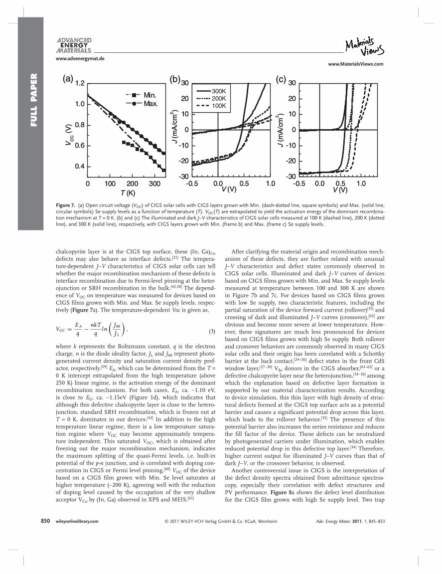
chalcopyrite layer is at the CIGS top surface, these (In, Ga) Cu defects may also behave as interface defects. [ 21 ] The tempera-ture-dependent J – V characteristics of CIGS solar cells can tell whether the major recombination mechanism of these defects is interface recombination due to Fermi-level pinning at the heter-ojunction or SRH recombination in the bulk. [ 42 , 58 ] The depend-ence of V OC on temperature was measured for devices based on CIGS fi lms grown with Min. and Max. Se supply levels, respec-tively ( Figure 7 a). The temperature-dependent Voc is given as,
VOC = E A
q− nkT
qln
(J00
JL
),
(3)
where k represents the Boltzmann constant, q is the electron charge, n is the diode ideality factor, J L and J 00 represent photo-generated current density and saturation current density pref-actor, respectively. [ 59 ] E A , which can be determined from the T = 0 K intercept extrapolated from the high temperature (above 250 K) linear regime, is the activation energy of the dominant recombination mechanism. For both cases, E A , ca. ∼ 1.10 eV, is close to E G , ca. ∼ 1.15eV (Figure 1 d), which indicates that although this defective chalcopyrite layer is close to the hetero-junction, standard SRH recombination, which is frozen out at T = 0 K, dominates in our devices. [ 42 ] In addition to the high temperature linear regime, there is a low temperature satura-tion regime where V OC may become approximately tempera-ture independent. This saturated V OC , which is obtained after freezing out the major recombination mechanism, indicates the maximum splitting of the quasi-Fermi levels, i.e. built-in potential of the p-n junction, and is correlated with doping con-centration in CIGS or Fermi level pinning. [ 60 ] V OC of the device based on a CIGS fi lm grown with Min. Se level saturates at higher temperature ( ∼ 200 K), agreeing well with the reduction of doping level caused by the occupation of the very shallow acceptor V Cu by (In, Ga) observed in XPS and MEIS. [ 61 ]
After clarifying the material origin and recombination mech-anism of these defects, they are further related with unusual J – V characteristics and defect states commonly observed in CIGS solar cells. Illuminated and dark J – V curves of devices based on CIGS fi lms grown with Min. and Max. Se supply levels measured at temperature between 100 and 300 K are shown in Figure 7 b and 7 c. For devices based on CIGS fi lms grown with low Se supply, two characteristic features, including the partial saturation of the device forward current (rollover) [ 35 ] and crossing of dark and illuminated J – V curves (crossover), [ 62 ] are obvious and become more severe at lower temperatures. How-ever, these signatures are much less pronounced for devices based on CIGS fi lms grown with high Se supply. Both rollover and crossover behaviors are commonly observed in many CIGS solar cells and their origin has been correlated with a Schottky barrier at the back contact, [ 24–26 ] defect states in the front CdS window layer, [ 27–30 ] V Se donors in the CIGS absorber, [ 63–65 ] or a defective chalcopyrite layer near the heterojunction, [ 34–36 ] among which the explanation based on defective layer formation is supported by our material characterization results. According to device simulation, this thin layer with high density of struc-tural defects formed at the CIGS top surface acts as a potential barrier and causes a signifi cant potential drop across this layer, which leads to the rollover behavior. [ 35 ] The presence of this potential barrier also increases the series resistance and reduces the fi ll factor of the device. These defects can be neutralized by photogenerated carriers under illumination, which enables reduced potential drop in this defective top layer. [ 34 ] Therefore, higher current output for illuminated J – V curves than that of dark J – V , or the crossover behavior, is observed.
Another controversial issue in CIGS is the interpretation of the defect density spectra obtained from admittance spectros-copy, especially their correlation with defect structures and PV performance. Figure 8 a shows the defect level distribution for the CIGS fi lm grown with high Se supply level. Two trap
Figure 7 . (a) Open circuit voltage ( V OC ) of CIGS solar cells with CIGS layers grown with Min. (dash-dotted line, square symbols) and Max. (solid line, circular symbols) Se supply levels as a function of temperature ( T ). V OC ( T ) are extrapolated to yield the activation energy of the dominant recombina-tion mechanism at T = 0 K. (b) and (c) The illuminated and dark J – V characteristics of CIGS solar cells measured at 100 K (dashed line), 200 K (dotted line), and 300 K (solid line), respectively, with CIGS layers grown with Min. (frame b) and Max. (frame c) Se supply levels.
0 100 200 300
0.4
0.6
0.8
1.0
1.2
VO
C (
V)
T (K)
Min. Max.
-0.5 0.0 0.5 1.0-30
-20
-10
0
10
20
30
J (m
A/c
m2 )
V (V)-0.5 0.0 0.5 1.0
-30
-20
-10
0
10
20
30 300K 200K 100K
J (m
A/c
m2)
V (V)
)c()b()a(
0 100 200 300
0.4
0.6
0.8
1.0
1.2
VO
C (
V)
T (K)
Min. Max.
-0.5 0.0 0.5 1.0-30
-20
-10
0
10
20
30
J (m
A/c
m2 )
V (V)-0.5 0.0 0.5 1.0
-30
-20
-10
0
10
20
30 300K 200K 100K
J (m
A/c
m2)
V (V)
)c()b()a(

851© 2011 WILEY-VCH Verlag GmbH & Co. KGaA, Weinheim
FULL P
APER
wileyonlinelibrary.com
www.MaterialsViews.comwww.advenergymat.de
Adv. Energy Mater. 2011, 1, 845–853
levels denoted as α and N1, with activation energies at around 25 and 110 meV, respectively, are present. With regard to the shallow defect, α , it is generally assigned to acceptors in CIGS originating from V Cu . [ 66 ] However, the origin of N1 is unclear. Previous experimental and simulation results have suggested the assignment of N1 as interface defects, [ 20 ] bulk defects in CIGS, [ 22 , 23 ] Schottky back contact, [ 26 ] V Se donors, [ 67 , 68 ] and the (In, Ga) Cu defects near the space charge region. [ 31–34 ] Our results directly establish the correlation between the N1 defect level and (In, Ga) Cu structural defects. For CIGS fi lms grown with low Se supply level, signifi cant increase of (In, Ga) Cu defects near the CIGS surface is suggested by XPS and MEIS results. This increase of (In, Ga) Cu defects also leads to the reduction of existing V Cu defects/acceptors. These changes are refl ected in their defect spectra. For CIGS fi lms grown with low Se supply level, the signifi cant increase of N1 defects, caused presum-ably by the increase of the (In, Ga) Cu defect density, is observed (Figure 8 b), while at the same time the α defect density dimin-ishes, agreeing well with the occupation of existing V Cu defects by (In, Ga) to form these extra (In, Ga) Cu defects, as suggested by surface composition characterization results. After corre-lating defect spectra with measured device PV performance (See Figure 1 ), we also confi rm the predicted detrimental effect of these relatively shallow donors, which can be converted to deep level recombination centers through lattice relaxations under photoexcitation, [ 39 ] on device power conversion effi ciency, although the moderate increase of deeper level—i.e., above 200 meV—trap density (Figure 8 b) may also partially account for the inferior PV performance of CIGS fi lms grown under low Se supply level. [ 69 ]
3. Conclusions
We summarize our results as follows: the Se supply level during CIGS grain growth is controlled to induce different levels of structural defects in CIGS fi lms, while keeping all other process
parameters identical to simplify the data interpretation. This process difference has negligible effect on CIGS grain struc-tures, crystal orientation, and bulk composition, as measured by cross-section SEM/TEM, XRD and SIMS. However, under insuffi cient Se supply level, a defective chalcopyrite layer with high density of (In, Ga) Cu defects forms near the CIGS surface, as suggested by XPS and MEIS results, due to the loss of Se from the CIGS lattice. This defective chalcopyrite layer leads to more pronounced rollover and crossover signatures observed in J – V curves. The occupation of existing V Cu by extra (In, Ga) atoms to form (In, Ga) Cu defects is also refl ected in their defect spectra, where signifi cant decrease of shallow acceptor defects, attributed to V Cu defects, but increase of the deeper N1 defect level, attributed to (In, Ga) Cu defects, are observed, compared with results from the same measurements performed on CIGS fi lms grown with high Se supply. The direct and signifi cant negative impact of those defects on solar cell PV performance by acting as SRH recombination centers is also established. These systematic comparative study results are not only impor-tant for understanding the materials science and defect physics of CIGS, especially clarifying the controversies about the origin of the unusual shape of the J – V characteristic and N1 defect level in admittance spectroscopy, but also useful for the further optimization of CIGS process conditions for better PV device performance.
4. Experimental Section PV Device Fabrication : CIGS fi lms were deposited from solution on
Mo-coated glass substrates as previously described, [ 7 , 8 , 40 ] followed by a CdS layer ( ∼ 60 nm thick), deposited with a standard chemical bath approach at 60 ° C to form the heterojunction. [ 70 ] Intrinsic ZnO (80 nm) and ITO (140 nm) were sputtered on top with a commercial RF magnetron sputtering system (Kurt Lesker). Finally, a Ni (50 nm)/ Al (2 μ m) grid was patterned with shadowed e-beam evaporation to facilitate carrier collection. No anti-refl ective coating was employed. Each device was separated using mechanical scribing, defi ning a device with an approximate area of 0.45 cm 2 .
Film Characterization : The grain structures of CIGS fi lms were characterized with cross-section SEM (Zeiss, Leo-1560) operated at 5 kV, after mechanical cleavage and a thin Au fi lm coating to prevent charging. TEM was performed using a JEOL 3000F operated at 300 kV. Cross-sectioned samples were prepared using the FEI Helios 400S DB-FIB. XRD data were collected with a Siemens D5000 diffractometer using Cu K α radiation. The comparative SIMS measurements were performed with a Cameca SC-Ultra instrument with cesium ion bombardment and quantitative SIMS measurements were performed at Evans Analytical Group as a service. CIGS surface roughness was measured with an AFM (Dimension 3000) in tapping mode. Sample surface compositions were measured in the near-surface region using XPS and MEIS. The XPS system used a Mg K α source, with photoelectrons collected at a 45 degree emission angle, giving an escape depth of approximately 1.5 nm. MEIS measurements were performed with 200 keV He + ions, using a toroidal electrostatic analyzer for detection of backscattered ions.
Device Characterization : The completed PV devices were characterized in air with a source meter (Keithley 2440) and a 1000 W Xe lamp solar simulator with 1.5 air mass fi lter (Oriel 91192) equipped with closed-loop light stabilization system. The light source was calibrated to 100 mWcm − 2 with a reference cell (Oriel 91150) each time before measurement. The capacitance was measured with a LCR meter (Hewlett-Packard 4192A). Temperature dependent measurement was carried out using a liquid
Figure 8 . Defect density of states ( N T ) calculated from admittance spec-troscopy for CIGS layers grown with Max. (frame a) and Min. (frame b) Se supply levels, measured for a T range of 100 ∼ 300 K with a step ( Δ T ) of 20 K and frequency ( f ) range of 100 Hz ∼ 1MHz. Trap levels with activation energies ( E ) at around 25 meV (dotted lines) and 110 meV (solid lines) are designated as α and N 1, respectively. Associated integrated N T s are calculated based on Gaussian fi tting.
100 200 300
1015
1016
1017
Energy E (meV)
NT (
cm-3
⋅eV-1
)
100 200 300
N1: 6.0×1013 cm-3α: 6.5×1014 cm-3Integrated NT
α
N1
100 200 300Energy E (meV)
NT (c
m-3
⋅eV-1
)100 200 300
1015
1016
1017
N1
T=100∼300KΔT=20Kf=100Hz ∼ 1MHzN1:4.9×10¹⁴ (cm-3)
b()a(
100 200 300
1015
1016
1017
Energy E (meV)
NT (
cm-3
⋅eV-1
)
100 200 300
N1: 6.0×1013 cm-3α: 6.5×1014 cm-3Integrated NT
α
N1
100 200 300Energy E (meV)
NT (c
m-3
⋅eV-1
)100 200 300
1015
1016
1017
N1
T=100∼300KΔT=20Kf=100Hz ∼ 1MHzN1:4.9×10¹⁴ (cm-3)
)()a(

852 © 2011 WILEY-VCH Verlag GmbH & Co. KGaA, Weinheim
FULL
PAPER
wileyonlinelibrary.com
www.MaterialsViews.comwww.advenergymat.de
Adv. Energy Mater. 2011, 1, 845–853
nitrogen (LN 2 ) cooled cryostat and a temperature controller (Lake Shore Cryotronics DRC-91C). QE and Refl ectivity were measured with Xe light source, monochromator, light chopper and lock-in amplifi er system (ProtoFlex QE 1400).
Acknowledgements We thank A. Prabhakar, Thomas Goislard de Monsabert, S. Thiruvengadam, and R. Ferlita for technical support with the preparation of substrates and Ni/Al grids. This work was conducted as part of a joint development project between Tokyo Ohka Kogyo Co., Ltd. and IBM Corporation.
Received: June 23, 2011 Published online:
[ 1 ] A. Shah , P. Torres , R. Tscharner , N. Wyrsch , H. Keppner , Science 1999 , 285 , 692 .
[ 2 ] D. Ginley , M. A. Green , R. Collins , MRS Bull. 2008 , 33 , 355 . [ 3 ] A. Romeo , A. Terheggen , D. Abou-Ras , D. L. Batzner , F. J. Haug ,
M. Kalin , D. Rudmann , A. N. Tiwari , Prog. Photovoltaics 2004 , 12 , 93 .
[ 4 ] Y. Yan , C. S. Jiang , R. Noufi , S. H. Wei , H. R. Moutinho , M. M. Al-Jassim , Phys. Rev. Lett. 2007 , 99 , 235504 .
[ 5 ] J. D. Beach , B. E. McCandless , MRS Bull. 2007 , 32 , 225 . [ 6 ] M. A. Green , K. Emery , Y. Hishikawa , W. Warta , Prog. Photovoltaics
2010 , 18 , 346 . [ 7 ] D. B. Mitzi , M. Yuan , W. Liu , A. J. Kellock , S. J. Chey , V. Deline ,
A. G. Schrott , Adv. Mater. 2008 , 20 , 3657 . [ 8 ] D. B. Mitzi , M. Yuan , W. Liu , A. J. Kellock , S. J. Chey , L. Gignac ,
A. G. Schrott , Thin Solid Films 2009 , 517 , 2158 . [ 9 ] W. W. Hou , B. Bob , S. H. Li , Y. Yang , Thin Solid Films 2009 , 517 ,
6853 . [ 10 ] V. K. Kapur , A. Bansal , P. Le , O. I. Asensio , Thin Solid Films 2003 ,
431 , 53 . [ 11 ] L. Li , N. Coates , D. Moses , J. Am. Chem. Soc. 2010 , 132 , 22 . [ 12 ] Q. Guo , G. M. Ford , H. W. Hillhouse , R. Agrawal , Nano Lett. 2009 ,
9 , 3060 . [ 13 ] H. W. Hillhouse , M. C. Beard , Curr. Opin. Colloid Interface Sci. 2009 ,
14 , 245 . [ 14 ] J. Tang , S. Hinds , S. O. Kelley , E. H. Sargent , Chem. Mat. 2008 , 20 ,
6906 . [ 15 ] R. N. Bhattacharya , W. Batchelor , J. F. Hiltner , J. R. Sites , Appl. Phys.
Lett. 1999 , 75 , 1431 . [ 16 ] T. Todorov , D. B. Mitzi , Eur. J. Inorg. Chem. 2010 , 2010 , 17 . [ 17 ] C. J. Hibberd , E. Chassaing , W. Liu , D. B. Mitzi , D. Lincot ,
A. N. Tiwari , Prog. Photovoltaics 2010 , 18 , 434 . [ 18 ] S. Siebentritt , M. Igalson , C. Persson , S. Lany , Prog. Photovoltaics
2010 , 18 , 390 . [ 19 ] P. K. Johnson , J. T. Heath , J. D. Cohen , K. Ramanathan , J. R. Sites ,
Prog. Photovoltaics 2005 , 13 , 579 . [ 20 ] R. Herberholz , M. Igalson , H. W. Schock , J. Appl. Phys. 1998 , 83 ,
318 . [ 21 ] M. Turcu , U. Rau , J. Phys. Chem. Solids. 2003 , 64 , 1591 . [ 22 ] J. T. Heath , J. D. Cohen , W. N. Shafarman , J. Appl. Phys. 2004 , 95 ,
1000 . [ 23 ] J. T. Heath , J. D. Cohen , W. N. Shafarman , Thin Solid Films 2003 ,
431 , 426 . [ 24 ] W. A. Miller , L. C. Olsen , IEEE Trans. Electron Devices 1984 , 31 , 654 . [ 25 ] M. Roy , S. Damaskinos , J. E. Phillips , The Conference Record of the
20th IEEE Photovoltaic Specialists Conference 1988 , 2, 1618 .
[ 26 ] T. Eisenbarth , T. Unold , R. Caballero , C. A. Kaufmann , H. W. Schock , J. Appl. Phys. 2010 , 107 , 034509 .
[ 27 ] J. Hou , S. J. Fonash , J. Kessler , in The Conference Record of the 25th IEEE Photovoltaic Specialists Conference , 1996 , 961 .
[ 28 ] M. Burgelman , F. Engelhardt , J. F. Guillemoles , R. Herberholz , M. Igalson , R. Klenk , M. Lampert , T. Meyer , V. Nadenau , A. Niemegeers , J. Parisi , U. Rau , H. W. Schock , M. Schmitt , O. Seifert , T. Walter , S. Zott , Prog. Photovoltaics 1997 , 5 , 121 .
[ 29 ] Z. Djebbour , A. Darga , A. M. Dubois , D. Mencaraglia , N. Naghavi , J. F. Guillemoles , D. Lincot , Thin Solid Films 2006 , 511 , 320 .
[ 30 ] M. Kontges , R. Reineke-Koch , P. Nollet , J. Beier , R. Schaffl er , J. Parisi , Thin Solid Films 2002 , 403 , 280 .
[ 31 ] M. Igalson , M. Edoff , Thin Solid Films 2005 , 480 , 322 . [ 32 ] D. Schmid , M. Ruckh , F. Grunwald , H. W. Schock , J. Appl. Phys.
1993 , 73 , 2902 . [ 33 ] T. Eisenbarth , T. Unold , R. Caballero , C. A. Kaufmann , D. Abou-Ras ,
H. W. Schock , Thin Solid Films 2009 , 517 , 2244 . [ 34 ] A. Niemegeers , M. Burgelman , R. Herberholz , U. Rau , D. Hariskos ,
H. W. Schock , Prog. Photovoltaics 1998 , 6 , 407 . [ 35 ] M. Topic , F. Smole , J. Furlan , Sol. Energy Mater. Sol. Cells 1997 , 49 ,
311 . [ 36 ] A. O. Pudov , A. Kanevce , H. A. Al-Thani , J. R. Sites , F. S. Hasoon , J.
Appl. Phys. 2005 , 97 , 064901 . [ 37 ] A. Rockett , D. Liao , J. T. Heath , J. D. Cohen , Y. M. Strzhemechny ,
L. J. Brillson , K. Ramanathan , W. N. Shafarman , Thin Solid Films 2003 , 431 , 301 .
[ 38 ] M. Igalson , M. Bodegard , L. Stolt , A. Jasenek , Thin Solid Films 2003 , 431 , 153 .
[ 39 ] S. Lany , A. Zunger , Phys. Rev. Lett. 2008 , 100 , 016401 . [ 40 ] M. Yuan , D. B. Mitzi , W. Liu , A. J. Kellock , S. J. Chey , V. R. Deline ,
Chem. Mat. 2010 , 22 , 285 . [ 41 ] A. M. Klimova , V. A. Ananichev , M. Arif , L. N. Blinov , Glass Phys.
Chem. 2005 , 31 , 760 . [ 42 ] S. S. Hegedus , W. N. Shafarman , Prog. Photovoltaics 2004 , 12 , 155 . [ 43 ] M. A. Contreras , M. J. Romero , R. Noufi , Thin Solid Films 2006 , 511 ,
51 . [ 44 ] D. Liao , A. Rockett , The Conference Record of the 28th IEEE Photo-
voltaic Specialists Conference 2000 , 446 . [ 45 ] S. B. Zhang , S. H. Wei , Phys. Rev. B 2002 , 65 , 081402 . [ 46 ] G. Hanna , J. Mattheis , V. Laptev , Y. Yamamoto , U. Rau , H. W. Schock ,
Thin Solid Films 2003 , 431 , 31 . [ 47 ] T. Wada , N. Kohara , S. Nishiwaki , T. Negami , Thin Solid Films 2001 ,
387 , 118 . [ 48 ] S. Nishiwaki , N. Kohara , T. Negami , T. Wada , Jpn. J. Appl. Phys. Part
2 - Lett. 1998 , 37 , L71 . [ 49 ] M. Gloeckler , J. R. Sites , W. K. Metzger , J. Appl. Phys. 2005 , 98 ,
113704 . [ 50 ] D. Azulay , O. Millo , I. Balberg , H. W. Schock , I. Visoly-Fisher ,
D. Cahen , Sol. Energy Mater. Sol. Cells 2007 , 91 , 85 . [ 51 ] T. Wada , N. Kohara , T. Negami , M. Nishitani , Jpn. J. Appl. Phys. Part
2 - Lett. 1996 , 35 , L 1253 . [ 52 ] W. Jaegermann , A. Klein , T. Mayer , Adv. Mater. 2009 , 21 , 4196 . [ 53 ] S. Nishiwaki , N. Kohara , T. Negami , H. Miyake , T. Wada , Jpn. J. Appl.
Phys. Part 1 - Regul. Pap. Short Notes Rev. Pap. 1999 , 38 , 2888 . [ 54 ] M. M. Islam , T. Sakurai , S. Ishizuka , A. Yamada , H. Shibata ,
K. Sakurai , K. Matsubara , S. Niki , K. Akimoto , J. Cryst. Growth 2009 , 311 , 2212 .
[ 55 ] M. Copel , IBM J. Res. Dev. 2000 , 44 , 571 . [ 56 ] S. B. Zhang , S. H. Wei , A. Zunger , H. Katayama-Yoshida , Phys. Rev.
B 1998 , 57 , 9642 . [ 57 ] J. C. Slater , J. Chem. Phys. 1964 , 41 , 3199 . [ 58 ] M. Turcu , O. Pakma , U. Rau , Appl. Phys. Lett. 2002 , 80 , 2598 . [ 59 ] V. Nadenau , U. Rau , A. Jasenek , H. W. Schock , J. Appl. Phys. 2000 ,
87 , 584 .

853© 2011 WILEY-VCH Verlag GmbH & Co. KGaA, Weinheim
FULL P
APER
wileyonlinelibrary.com
www.MaterialsViews.comwww.advenergymat.de
Adv. Energy Mater. 2011, 1, 845–853
[ 60 ] S. S. Hegedus , B. E. McCandless , Sol. Energy Mater. Sol. Cells 2005 , 88 , 75 .
[ 61 ] C. P. Thompson , S. Hegedus , W. Shafarman , D. Desai , The Confer-ence Record of the 33rd IEEE Photovoltaic Specialists Conference 2008 , 1 .
[ 62 ] M. Gloeckler , C. R. Jenkins , J. R. Sites , Mater. Res. Soc. Symp. Proc. 2003 , 763 , 231 .
[ 63 ] M. Igalson , P. Zabierowski , D. Przado , A. Urbaniak , M. Edoff , W. N. Shafarman , Sol. Energy Mater. Sol. Cells 2009 , 93 , 1290 .
[ 64 ] S. Lany , A. Zunger , Phys. Rev. B 2005 , 72 , 035215 . [ 65 ] S. Lany , A. Zunger , J. Appl. Phys. 2006 , 100 , 113725 .
[ 66 ] J. Vidal , S. Botti , P. Olsson , J. F. Guillemoles , L. Reining , Phys. Rev. Lett. 2010 , 104 , 056401 .
[ 67 ] T. Sakurai , N. Ishida , S. Ishizuka , M. M. Islam , A. Kasai , K. Matsubara , K. Sakurai , A. Yamada , K. Akimoto , S. Niki , Thin Solid Films 2008 , 516 , 7036 .
[ 68 ] M. Igalson , A. Urbaniak , M. Edoff , Thin Solid Films 2009 , 517 , 2153 . [ 69 ] T. Sakurai , M. M. Islam , H. Uehigashi , S. Ishizuka , A. Yamada ,
K. Matsubara , S. Niki , K. Akimoto , Sol. Energy Mater. Sol. Cells 2011 , 95 , 227 .
[ 70 ] M. A. Contreras , M. J. Romero , B. T. E. Hasoon , R. Noufi , S. Ward , K. Ramanathan , Thin Solid Films 2002 , 403 , 204 .