defect evolution in ultralow energy, high dose helium
TRANSCRIPT
J. Appl. Phys. 124, 165708 (2018); https://doi.org/10.1063/1.5046096 124, 165708
© 2018 Author(s).
Defect evolution in ultralow energy, highdose helium implants of silicon performed atelevated temperaturesCite as: J. Appl. Phys. 124, 165708 (2018); https://doi.org/10.1063/1.5046096Submitted: 25 June 2018 . Accepted: 10 October 2018 . Published Online: 26 October 2018
K. Haynes , X. Hu, B. D. Wirth, C. Hatem, and K. S. Jones
ARTICLES YOU MAY BE INTERESTED IN
Bandlike and localized states of extended defects in n-type In0.53Ga0.47As
Journal of Applied Physics 124, 165707 (2018); https://doi.org/10.1063/1.5046827
Electrical hysteresis of ultrathin silicon oxides induced by heavy boron dopingJournal of Applied Physics 124, 165107 (2018); https://doi.org/10.1063/1.5039651
Surface patterning of monocrystalline silicon induced by spot laser meltingJournal of Applied Physics 124, 163104 (2018); https://doi.org/10.1063/1.5049781
Defect evolution in ultralow energy, high dose helium implants of siliconperformed at elevated temperatures
K. Haynes,1,a) X. Hu,2 B. D. Wirth,2,3 C. Hatem,4 and K. S. Jones11Department of Materials Science and Engineering, University of Florida, Gainesville, Florida 32611, USA2Oak Ridge National Laboratory, Oak Ridge, Tennessee 37831, USA3Department of Nuclear Engineering, University of Tennessee, Knoxville, Tennessee 37996, USA4Applied Materials, Gloucester, Massachusetts 01930, USA
(Received 25 June 2018; accepted 10 October 2018; published online 26 October 2018)
There is a growing interest in using high dose helium implants to alter point defect populations insilicon. Previous reports have shown that the interaction between helium and vacancies leads to theformation of cavities for medium energy (e.g., 20–100 keV) implants. However, the role of certainfactors, such as the proximity of the surface, the damage created by the implant, and the effect ofthe implant temperature, is not well understood for low energy implants. This study explored a newregime of ultralow energy, elevated temperature implants in order to offer an insight into the effectof these parameters. Transmission electron microscopy (TEM) showed that cavity formation wasavoided for 0.5 keV, 450 °C implants up to a dose of 8 × 1016 cm−2. However, extended defects inthe form of {311} ribbon-like defects and stacking faults were observed. Quantitative TEM showedthat the number of interstitials in these defects was less than 0.2% of the implant dose. In addition,thermal helium desorption spectrometry suggested that only 2% of the implanted He dose wasretained in interstitial He and HemVn complexes. A first-order dissociation kinetic model wasapplied to assess desorption from HemVn, which closely matched energies predicted by densityfunctional theory. This population of excess vacancies and excess interstitials was possibly formedbecause of incomplete Frenkel pair recombination. Raman spectroscopy showed that the stress fromthe implant was dominated by the stress from the interstitial-type defects. The evolution of the stressand defects was also explored as a function of post-implant annealing. Published by AIPPublishing. https://doi.org/10.1063/1.5046096
I. INTRODUCTION
High-dose, medium-energy He implants in Si are knownto result in the formation of He bubbles.1 Upon high tempera-ture annealing, these bubbles outgas He and grow into largercavities via either migration and coalescence2,3 or anOstwald-ripening process.4,5 Many studies have explored themorphology and evolution of these cavities,5 which have appli-cations for ion-cut technology,6 gettering transition metal impu-rities,7,8 gettering dopants,9–11 and reducing interstitialpopulations.12,13
Cavity formation is believed to occur because of the inter-action between He and vacancies. Due to its low solubility inSi, He is energetically driven to occupy sites with the largestavailable free volume. When He is introduced into Si by ionimplantation, elastic collisions generate a large number ofvacancies and self-interstitials. These point defects are mobileeven at room temperature in Si and will either recombine withone another or form larger defect clusters. Helium will prefer-entially occupy vacancy clusters, and multiple He atoms canbe accommodated within these vacancy clusters,14 leading tothe formation of HemVn complexes of varying sizes. Theseclusters are precursors to larger He bubbles.
HemVn clusters could be used as a source of vacanciesfor improving dopant activation. Modern devices may require
dopant activation levels in excess of their solid solubilities inSi, and it is often not possible to use dopant activation methodssuch as melting or solid-phase epitaxial regrowth with 3Ddevice architectures.15 Vacancy engineering approaches areneeded, and He may be able to disrupt self-interstitial-vacancyrecombination in favor of excess vacancies.
Because of the strong interaction of He with the pointdefects generated by the implantation process, changes to theimplant conditions can have a dramatic effect on the defectstructures that are generated. Elevated temperature He implantshave been shown to result in different defect structures com-pared to room temperature implants.16–20 A lower density oflarger He bubbles is formed at moderate implant temperatures(e.g., 200–600 °C), while bubble formation is entirely sup-pressed at higher implant temperatures.19 Extended defectshave also been observed in the form of {311} rod- and ribbon-like defects and dislocation loops.19 This range of defectsreflects the complex kinetics of the atomic processes involved,which include self-interstitial-vacancy recombination, pointdefect diffusion, and He diffusion, as well as the relative stabil-ities of various defect complexes at different temperatures.
Previous studies of elevated temperature He implantswere completed for implant energies greater than 20 keV.This results in projected ranges in excess of 200 nm due tothe light mass of He. There have been few studies on lowenergy implantation of He into Si.21,22 The proximity of thesurface is expected to play a role in He implantationa)Author to whom correspondence should be addressed: [email protected]
JOURNAL OF APPLIED PHYSICS 124, 165708 (2018)
0021-8979/2018/124(16)/165708/7/$30.00 124, 165708-1 Published by AIP Publishing.

dynamics, as it can act as a sink for either self-interstitials orvacancies, as well as He desorption. In addition, lowerenergy implants generate fewer Frenkel pairs per ion, whichis likely to impact their interaction with He.
In this study, the defect evolution of ultralow energy,elevated temperature He implants is investigated. Cavity for-mation and other defect structures are found to vary widelyfrom their corresponding higher energy implants. Thedynamics of He and point defect interactions is explored,which offers some insight into the evolution of Frenkel pairsin the absence of excess interstitials that are typically gener-ated by implanting dopant species.
II. EXPERIMENT
He+ was implanted into n-type Czochralski-grown (100)Si at 450 °C using an implantation energy of 0.5 keV. Doseswere varied from 5 × 10¹⁵ to 8 × 1016 cm−2 and beam currentsof approximately 4 mA were used. Both rapid thermal anneals(RTA) and furnace anneals were investigated for temperaturesbetween 500 °C and 1000 °C under an Ar ambient.
Damage evolution was monitored by cross-section andplan-view transmission electron microscopy (TEM). Cross-sections were prepared with a focused ion beam usingstandard methods. Self-supported plan-view samples wereprepared by coring 3-mm discs, which were then polishedand etched from the backside to obtain regions of electrontransparency. TEM characterization was performed on an FEITecnai F20 microscope using [110] zone axis imaging condi-tions for the cross-sections and g220 weak beam dark field(WBDF) imaging conditions for the plan-view samples.
Raman spectroscopy was used to determine stress in theimplanted region. Spectra were collected on an HoribaAramis microRaman system with an excitation wavelength of325 nm. This wavelength has a penetration depth of approxi-mately 10 nm, which closely matches the depth of theimplants investigated.
Thermal helium desorption spectrometry (THDS) wasused to measure the desorption of He as a function of tem-perature for a constant ramp rate of 0.5 °C/s up to 1250 °C.Released He was measured by a quadrupole mass spectrome-ter. The ultra-high vacuum chamber (∼1 × 10⁻⁹ Torr) pro-vides a low He background of 2 × 10¹⁰ He/s. Measurementswere calibrated with a high-precision glass-permeationhelium calibrated leak.
III. RESULTS AND DISCUSSION
Depth distributions for He and for Frenkel pairs gener-ated by the implant were calculated using SRIM-2013, aMonte Carlo simulation program.23 Results are shown for the2 × 1016 cm−2 dose in Fig. 1. The projected range for He is8.6 nm with the peak concentration located at 6.8 nm, whilethe peak of the vacancy distribution is at a depth of 3.6 nm.On average, each He ion generates 8 Frenkel pairs, accordingto SRIM. However, SRIM does not account for thermaleffects, such as diffusion or recombination of implantedspecies or point defects. Thus, this simulation is an estimateof the distribution of Frenkel pairs generated during theimplant. It is expected that most of these Frenkel pair defects
will either recombine at the 450 °C implant temperature orannihilate at the free surface, leaving only a small fraction ofthe initial point defect population behind. Likewise, somefraction of the interstitial helium will likely diffuse back tothe surface and desorb.
He bubble formation in Si has been found to be primarilydependent on the local He concentration for room temperatureimplants. When concentrations exceed 3 (±1) × 1020 cm−3,bubbles have been observed.7 Based on the peak concentra-tions of He for the doses in this study, all samples would beexpected to form He bubbles if 100% of the implanted heliumwere retained. However, some fraction is likely to diffuse out atthe high implant temperature. It should also be noted that a sig-nificant portion (21%) of the incident ions are reflected (back-scattered) from the sample without implanting. In addition,sputtering effects are non-negligible for the two highest doses.SRIM estimates that approximately 3.1 and 1.6 nm are sput-tered from the surface for a dose of 8 × 10¹⁶ and 4 × 1016 cm−2,respectively. Using an iterative method to account for themoving surface during implantation,24 the amount of He lostdue to sputtering is estimated to be less than 6% and 3%,respectively. Adjusted ion and vacancy profiles for the highestdose are provided in the supplementary material.
TEM cross-sections were prepared for each of theimplanted doses, as shown in the high-resolution TEM(HRTEM) images in Fig. 2. No He bubbles were visible, evenfor the highest doses. However, extended defects were visiblefor doses above 5 × 1015 cm−2. Stacking faults along {111}planes and ribbon-like {311} defects were both observed(Fig. 3). The defect density appeared to increase proportionallywith the dose. The defects were largely present within 30 nmof the surface, corresponding to the damage profile predictedby SRIM. However, some of the defects were located consider-ably deeper, up to 60 nm beneath the surface. This indicatesthat the point defects that make up the extended defects werevery mobile at the implant temperature and may have nucleatedheterogeneously on an impurity or pre-existing defect.
Fast Fourier Transform (FFT) filtering was used to inves-tigate the nature of the extended defects. Implant damage istypically interstitial in nature, as explained by the “plus-one”model.25 Most interstitial-vacancy pairs recombine during
FIG. 1. SRIM simulations for the He distribution and vacancy distributionfor a 2 × 10¹⁶ He/cm2 implant at 0.5 keV.
165708-2 Haynes et al. J. Appl. Phys. 124, 165708 (2018)

implantation and upon annealing, leaving behind a quantityof interstitials that is approximately equal to the implanteddose. However, He is dynamically removed during elevatedtemperature implant, and the dominant observable defectsafter He implantation are generally cavities, i.e., largevacancy clusters that may contain He. Therefore, the natureof these extended defects needs to be carefully examined todetermine whether it is intrinsic or extrinsic. A representativeHRTEM image of a stacking fault and an FFT filtered imageare shown in Fig. 4. The lattice fringes clearly bow outwardaround the stacking fault, indicating that it is made up of aninserted plane of atoms and confirming its extrinsic nature.
The fact that cavities were not formed is a departure fromhigher energy studies that were completed at similar implanttemperatures and doses. David and Oliviero observed cavityformation for 50 keV 5 × 10¹⁶ He/cm2 implants completed atimplant temperatures up to 600 °C.18,19,26,27 Bubble formationdid not occur in this study. This may indicate that the proximityof the surface allows He to escape more efficiently than for ahigher energy implant. It could also be related to the lowernumber of vacancies generated. According to SRIM calcula-tions, a 0.5 keV implant creates about 8 vacancies/ion com-pared to ∼166 vacancies/ion for a 50 keV implant. Despite thisdifference in He bubble formation, the interstitial-type defectsobserved are similar to the higher-energy implantation studies,which also noted rod-like defects, ribbon-like defects, and dis-location loops for temperatures above 600 °C. Babonneau alsoobserved {311} rod- and ribbon-like defects following 50 keV
FIG. 2. Cross-sectional HRTEM images of Si implanted at 0.5 keV and 450 °C with (a) 5 × 10¹⁵, (b) 1 × 10¹⁶, (c) 2 × 10¹⁶, (d) 4 × 10¹⁶, and (e) 8 × 10¹⁶ He/cm2.The projected range of the He is indicated by a dashed line.
FIG. 3. Extended defects for an 8 × 10¹⁶ He/cm2 implant at 0.5 keV and 450 °Cincluded both stacking faults (SF) along {111} planes and {311} ribbon-like(RL) defects.
FIG. 4. (a) HRTEM image of a stacking fault following a 0.5 keV, 450 °Cimplant. (b) An FFT filtered image shows the lattice fringes bowing aroundthe stacking fault, indicating its extrinsic nature.
165708-3 Haynes et al. J. Appl. Phys. 124, 165708 (2018)
helium implantation to a dose of 7 × 10¹⁵ He/cm2 at implanttemperatures above 300 °C.20
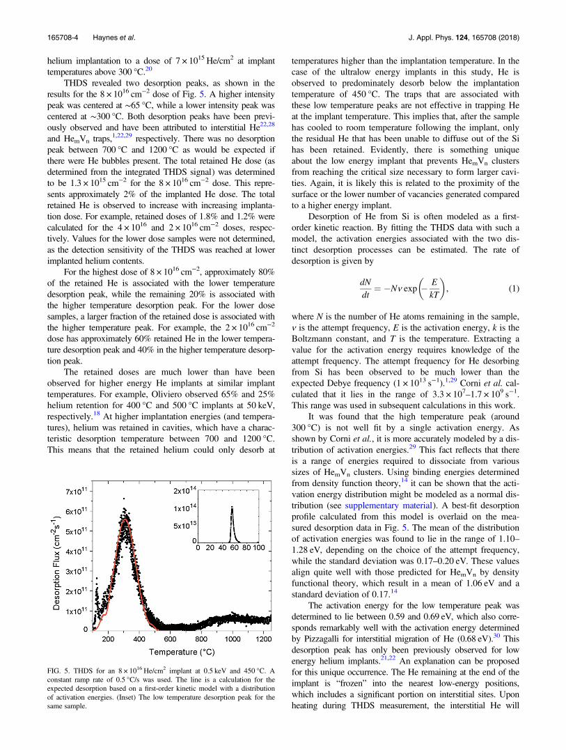
THDS revealed two desorption peaks, as shown in theresults for the 8 × 1016 cm−2 dose of Fig. 5. A higher intensitypeak was centered at ∼65 °C, while a lower intensity peak wascentered at ∼300 °C. Both desorption peaks have been previ-ously observed and have been attributed to interstitial He22,28
and HemVn traps,1,22,29 respectively. There was no desorptionpeak between 700 °C and 1200 °C as would be expected ifthere were He bubbles present. The total retained He dose (asdetermined from the integrated THDS signal) was determinedto be 1.3 × 1015 cm−2 for the 8 × 1016 cm−2 dose. This repre-sents approximately 2% of the implanted He dose. The totalretained He is observed to increase with increasing implanta-tion dose. For example, retained doses of 1.8% and 1.2% werecalculated for the 4 × 10¹⁶ and 2 × 1016 cm−2 doses, respec-tively. Values for the lower dose samples were not determined,as the detection sensitivity of the THDS was reached at lowerimplanted helium contents.
For the highest dose of 8 × 1016 cm−2, approximately 80%of the retained He is associated with the lower temperaturedesorption peak, while the remaining 20% is associated withthe higher temperature desorption peak. For the lower dosesamples, a larger fraction of the retained dose is associated withthe higher temperature peak. For example, the 2 × 1016 cm−2
dose has approximately 60% retained He in the lower tempera-ture desorption peak and 40% in the higher temperature desorp-tion peak.
The retained doses are much lower than have beenobserved for higher energy He implants at similar implanttemperatures. For example, Oliviero observed 65% and 25%helium retention for 400 °C and 500 °C implants at 50 keV,respectively.18 At higher implantation energies (and tempera-tures), helium was retained in cavities, which have a charac-teristic desorption temperature between 700 and 1200 °C.This means that the retained helium could only desorb at
temperatures higher than the implantation temperature. In thecase of the ultralow energy implants in this study, He isobserved to predominately desorb below the implantationtemperature of 450 °C. The traps that are associated withthese low temperature peaks are not effective in trapping Heat the implant temperature. This implies that, after the samplehas cooled to room temperature following the implant, onlythe residual He that has been unable to diffuse out of the Sihas been retained. Evidently, there is something uniqueabout the low energy implant that prevents HemVn clustersfrom reaching the critical size necessary to form larger cavi-ties. Again, it is likely this is related to the proximity of thesurface or the lower number of vacancies generated comparedto a higher energy implant.
Desorption of He from Si is often modeled as a first-order kinetic reaction. By fitting the THDS data with such amodel, the activation energies associated with the two dis-tinct desorption processes can be estimated. The rate ofdesorption is given by
dN
dt¼ �Nν exp � E
kT
� �, (1)
where N is the number of He atoms remaining in the sample,ν is the attempt frequency, E is the activation energy, k is theBoltzmann constant, and T is the temperature. Extracting avalue for the activation energy requires knowledge of theattempt frequency. The attempt frequency for He desorbingfrom Si has been observed to be much lower than theexpected Debye frequency (1 × 10¹³ s−1).1,29 Corni et al. cal-culated that it lies in the range of 3.3 × 10⁷–1.7 × 10⁹ s−1.This range was used in subsequent calculations in this work.
It was found that the high temperature peak (around300 °C) is not well fit by a single activation energy. Asshown by Corni et al., it is more accurately modeled by a dis-tribution of activation energies.29 This fact reflects that thereis a range of energies required to dissociate from varioussizes of HemVn clusters. Using binding energies determinedfrom density function theory,14 it can be shown that the acti-vation energy distribution might be modeled as a normal dis-tribution (see supplementary material). A best-fit desorptionprofile calculated from this model is overlaid on the mea-sured desorption data in Fig. 5. The mean of the distributionof activation energies was found to lie in the range of 1.10–1.28 eV, depending on the choice of the attempt frequency,while the standard deviation was 0.17–0.20 eV. These valuesalign quite well with those predicted for HemVn by densityfunctional theory, which result in a mean of 1.06 eV and astandard deviation of 0.17.14
The activation energy for the low temperature peak wasdetermined to lie between 0.59 and 0.69 eV, which also corre-sponds remarkably well with the activation energy determinedby Pizzagalli for interstitial migration of He (0.68 eV).30 Thisdesorption peak has only been previously observed for lowenergy helium implants.21,22 An explanation can be proposedfor this unique occurrence. The He remaining at the end of theimplant is “frozen” into the nearest low-energy positions,which includes a significant portion on interstitial sites. Uponheating during THDS measurement, the interstitial He will
FIG. 5. THDS for an 8 × 10¹⁶ He/cm2 implant at 0.5 keV and 450 °C. Aconstant ramp rate of 0.5 °C/s was used. The line is a calculation for theexpected desorption based on a first-order kinetic model with a distributionof activation energies. (Inset) The low temperature desorption peak for thesame sample.
165708-4 Haynes et al. J. Appl. Phys. 124, 165708 (2018)

diffuse along tetrahedral-hexagonal sites, and some He willreach the surface without becoming trapped. This process isvery unlikely for higher energy implants, in which interstitialHe is likely to become trapped by the high density of vacan-cies, HemVn clusters, or He bubbles that lie between the pro-jected range of He and the Si surface. This theory issupported by the literature. Corni et al. observed a delay timefor isothermal desorption of He, which could only beexplained by interstitial He trapping and detrapping fromvacancy-like defects.31 This supports the idea that interstitialHe is present for higher energy implants as well, but it isunlikely to reach the surface without becoming trapped.
Stress evolution as a function of increasing He dose wasstudied using Raman spectroscopy. Raman spectroscopy haspreviously been used to quantify stress in H- andHe-implanted Si.32,33 In these earlier works, the resultingstress was tied to the size and morphology of the sphericalnanobubbles or platelets that are formed. No such bubbleswere formed by the implants in this study. In addition, much
of the initial He dose has diffused out of the material.Therefore, by elimination, any stress must be closely associ-ated with the extended defects and defect clusters created bythe implant.
The primary Raman-active peak for Si is a three-folddegenerate longitudinal optical (LO) mode at 520.7 cm−1.Under stress, this peak splits and a peak shift is induced.Assuming a biaxial stress state, the magnitude of the in-planestress σ is linearly related to the magnitude of the frequencyshift Δω by
σ (MPa) ¼ �250 � Δω (cm�1), (2)
as has been derived elsewhere.34 From this equation, it canbe seen that a compressive stress will induce an increase inthe Raman frequency while a tensile stress will induce adecrease. Using a fitting procedure, the peak position can bedetermined within approximately 0.1 cm−1, allowing thedetection of stresses as low as 25MPa.
FIG. 6. (a) Raman spectra for the as-implanted samples show increasing blue shifts with increasing He dose. (b) Compressive stresses were calculated from themagnitude of the peak shift. Error bars are 95% confidence intervals based on multiple measurements across a single sample.
FIG. 7. (a) Raman spectra for the 8 × 1016 cm−2 implant following RTA spike anneals at temperatures from 500 to 1000 °C. (b) Stresses calculated from themagnitude of the peak shifts following annealing for three of the implant doses.
165708-5 Haynes et al. J. Appl. Phys. 124, 165708 (2018)
Raman spectra for the as-implanted samples are shownin Fig. 6. A Gaussian-Lorentzian fitting procedure was usedto determine the peak position. The LO peak shifted tohigher Raman frequencies with He implantation. The stressincreased monotonically with increasing dose, up to amaximum value of 1 GPa for the 8 × 1016 cm−2 dose. Thefull-width at half-maximum of the peaks also increased withHe dose, which can be attributed to the lattice disordercreated by the implant.
Generally, self-interstitial defect clusters are expected toinduce compressive stresses, while vacancy defect clustersshould induce tensile stresses. Given the different configura-tions taken by interstitial and vacancy clusters as well as thevariety of cluster sizes that are likely to be present, it is not pos-sible to deduce the relative concentrations of interstitials andvacancies from these stress measurements. However, it appearsthat the compressive stresses induced by the interstitial-typedefects dominate the overall stress of the system.
Stress was also monitored as a function of annealingtemperature for spike anneals performed between 500 °C and1000 °C. The Raman spectra for the 8 × 1016 cm−2 dose areshown in Fig. 7. For this dose, the Raman peak positionremained relatively constant around 524.0 cm−1 until the 800°C anneal. At this point, the peak shifted back toward theunstrained peak position but never fully reached theunstressed state. This is roughly the temperature at whichself-interstitial-type defects are known to evolve followingimplantation,35 which supports the theory that the stress stateis closely tied to the defect clusters. Furthermore, as shownby the THDS results of Fig. 6, the majority of the retainedHe has desorbed by 800 °C. A similar shift in peak positionwas noted for the lower dose samples but with smaller mag-nitude shifts toward the unstressed state.
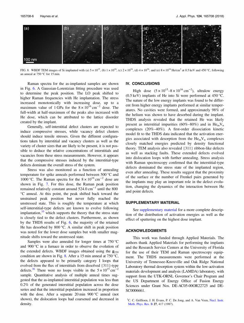
Samples were also annealed for longer times at 750 °Cand 900 °C in a furnace in order to observe the evolution ofthe extended defects. WBDF images obtained using the g220condition are shown in Fig. 8. After a 15min anneal at 750 °C,the defects appeared to be primarily category I loops thatevolved from the flux of interstitials from dissolved {311}-typedefects.36 There were no loops visible in the 5 × 1015 cm−2
sample. Quantitative analysis of multiple anneal times sug-gested that the as-implanted interstitial population was less than0.2% of the generated interstitial population across the doseseries and that the interstitial population increased in proportionwith the dose. After a separate 20min 900 °C anneal (notshown), the dislocation loops had coarsened and decreased indensity.
IV. CONCLUSIONS
High dose (5 × 10¹⁵–8 × 1016 cm−2), ultralow energy(0.5 keV) implants of He into Si were performed at 450 °C.The nature of the low energy implants was found to be differ-ent from higher energy implants performed at similar temper-atures. No cavities were formed, and approximately 98% ofthe helium was shown to have desorbed during the implant.THDS analysis revealed that the retained He was likelypresent as interstitial impurities (60%–80%) and in HemVn
complexes (20%–40%). A first-order dissociation kineticmodel fit to the THDS data indicated that the activation ener-gies associated with desorption from the HemVn complexesclosely matched energies predicted by density functionaltheory. TEM analysis also revealed {311} ribbon-like defectsas well as stacking faults. These extended defects evolvedinto dislocation loops with further annealing. Stress analysiswith Raman spectroscopy confirmed that the interstitial-typedefects dominated the stress state of the implanted region,even after annealing. These results suggest that the proximityof the surface or the number of Frenkel pairs generated bythe implants may play an important role in the defect evolu-tion, changing the dynamics of the interaction between Heand point defects.
SUPPLEMENTARY MATERIAL
See supplementary material for a more complete descrip-tion of the distribution of activation energies as well as theeffect of sputtering on the highest dose implant.
ACKNOWLEDGMENTS
This work was funded through Applied Materials. Theauthors thank Applied Materials for performing the implantsand the Research Service Centers at the University of Floridafor the use of their TEM and Raman spectroscopy equip-ment. The THDS measurements were performed at theUniversity of Tennessee-Knoxville and Oak Ridge NationalLaboratory thermal desorption system within the low-activationmaterials development and analysis (LAMDA) laboratory, withsupport from the UTK-ORNL Governor’s Chair Program andthe US Department of Energy Office of Fusion EnergySciences under Grant Nos. DE-AC05-00OR22725 and DE-SC0006661.
1C. C. Griffioen, J. H. Evans, P. C. De Jong, and A. Van Veen, Nucl. Instr.Meth. Phys. Res. B 27, 417 (1987).
FIG. 8. WBDF TEM images of Si implanted with (a) 5 × 10¹⁵, (b) 1 × 10¹⁶, (c) 2 × 10¹⁶, (d) 4 × 10¹⁶, and (e) 8 × 10¹⁶ He/cm2 at 0.5 keV and 450 °C, followingan anneal at 750 °C for 15 min.
165708-6 Haynes et al. J. Appl. Phys. 124, 165708 (2018)

2J. Evans, Nucl. Instr. Meth. Phys. Res. B 196, 125 (2002).3M. Hasanuzzaman, Y. M. Haddara, and A. P. Knights, J. Appl. Phys. 112,064302 (2012).4S. Frabboni, F. Corni, C. Nobili, R. Tonini, and G. Ottaviani, Phys. Rev. B69, 165209 (2004).5V. Raineri, M. Saggio, and E. Rimini, J. Mater. Res. 15, 1449 (2000).6M. Bruel, Electron. Lett. 31, 1201 (1995).7V. Raineri, P. G. Fallica, G. Percolla, A. Battaglia, M. Barbagallo, andS. U. Campisano, J. Appl. Phys. 78, 3727 (1995).8F. Roqueta, L. Ventura, J. J. Grob, and R. Jérisian, J. Appl. Phys. 88, 5000(2000).9F. Cayrel, D. Alquier, L. Ventura, and F. Roqueta, Eur. Phys. J. Appl.Phys. 23, 41 (2003).
10F. Roqueta, D. Alquier, L. Ventura, C. Dubois, and R. Jérisian, Nucl. Instr.Meth. Phys. Res. B 183, 318 (2001).
11F. Cayrel, D. Alquier, D. Mathiot, L. Ventura, L. Vincent, G. Gaudin, andR. Jerisian, Nucl. Instr. Meth. Phys. Res. B 216, 291 (2004).
12V. Raineri and S. U. Campisano, Appl. Phys. Lett. 69, 1783 (1996).13M. L. David, M. F. Beaufort, and J. F. Barbot, Nucl. Instr. Meth. Phys.Res. B 226, 531 (2004).
14L. Pizzagalli, M.-L. David, and J. Dérès, Phys. Status Solidi 214, 1700263(2017).
15R. Duffy, M. J. H. Van Dal, B. J. Pawlak, M. Kaiser, R. G. R. Weemaes,B. Degroote, E. Kunnen, and E. Altamirano, Appl. Phys. Lett. 90, 241912(2007).
16V. Raineri and M. Saggio, Appl. Phys. Lett. 71, 1673 (1997).17P. F. Fichtner, A. Peeva, M. Behar, G. d. M. Azevedo, R. Maltez, R. Koegler,and W. Skorupa, Nucl. Instr. Meth. Phys. Res. B 161–163, 1038 (2000).
18E. Oliviero, M. L. David, M. F. Beaufort, J. F. Barbot, and A. van Veen,Appl. Phys. Lett. 81, 4201 (2002).
19M. L. David, M. F. Beaufort, and J. F. Barbot, J. Appl. Phys. 93, 1438(2003).
20D. Babonneau, M.-F. Beaufort, A. Declémy, J.-F. Barbot, and J.-P. Simon,J. Appl. Phys. 99, 113507 (2006).
21A. L. M. Davies and G. Carter, Radiat. Eff. 10, 227 (1971).22A. Van Veen, H. Schut, R. A. Hakvoort, A. Fedorov, and K. T.Westerduin, MRS Proc. 373, 499 (1994).
23J. F. Ziegler, M. D. Ziegler, and J. P. Biersack, Nucl. Instr. Meth. Phys.Res. B 268, 1818 (2010).
24J. Wang, M. B. Toloczko, N. Bailey, F. A. Garner, J. Gigax, and L. Shao,Nucl. Instr. Meth. Phys. Res. B 387, 20 (2016).
25M. D. Giles, J. Electrochem. Soc. 138, 1160 (1991).26E. Oliviero, M. L. David, A. V. Fedorov, A. van Veen, M. F. Beaufort,and J. F. Barbot, Mater. Sci. Eng. B 102, 222 (2003).
27M. David, A. Ratchenkova, E. Oliviero, M. Denanot, M. Beaufort,A. Declémy, C. Blanchard, N. Gerasimenko, and J. Barbot, Nucl. Instr.Meth. Phys. Res. B 198, 83 (2002).
28A. Van Veen, P. C. De Jong, K. R. Bijkerk, H. A. Filius, and J. H. Evans,MRS Proc. 100, 231 (1988).
29F. Corni, C. Nobili, G. Ottaviani, R. Tonini, G. Calzolari, G. F. Cerofolini,and G. Queirolo, Phys. Rev. B 56, 7331 (1997).
30L. Pizzagalli and A. Charaf-Eddin, Semicond. Sci. Technol. 30, 085022(2015).
31F. Corni, G. Calzolari, S. Frabboni, C. Nobili, G. Ottaviani, R. Tonini,G. F. Cerofolini, D. Leone, M. Servidori, R. S. Brusa, G. P. Karwasz,N. Tiengo, and A. Zecca, J. Appl. Phys. 85, 1401 (1999).
32C. Villeneuve, V. Paillard, K. K. Bourdelle, I. Cayrefourcq, A. Boussagol,and M. Kennard, Nucl. Instr. Meth. Phys. Res. B 253, 182 (2006).
33C. Villeneuve, K. K. Bourdelle, V. Paillard, X. Hebras, and M. Kennard,J. Appl. Phys. 102, 094905 (2007).
34I. De Wolf, Semicond. Sci. Technol. 11, 139 (1996).35K. S. Jones, S. Prussin, and E. R. Weber, Appl. Phys. A Solids Surf. 45, 1(1988).
36J. Li and K. S. Jones, Appl. Phys. Lett. 73, 3748 (1998).
165708-7 Haynes et al. J. Appl. Phys. 124, 165708 (2018)